EP3343544A1 - Method for a display device - Google Patents
Method for a display device Download PDFInfo
- Publication number
- EP3343544A1 EP3343544A1 EP16206859.7A EP16206859A EP3343544A1 EP 3343544 A1 EP3343544 A1 EP 3343544A1 EP 16206859 A EP16206859 A EP 16206859A EP 3343544 A1 EP3343544 A1 EP 3343544A1
- Authority
- EP
- European Patent Office
- Prior art keywords
- dedicated
- pixels
- dedicated pixels
- pixel
- micrometers
- Prior art date
- Legal status (The legal status is an assumption and is not a legal conclusion. Google has not performed a legal analysis and makes no representation as to the accuracy of the status listed.)
- Granted
Links
Images





Classifications
-
- G—PHYSICS
- G09—EDUCATION; CRYPTOGRAPHY; DISPLAY; ADVERTISING; SEALS
- G09G—ARRANGEMENTS OR CIRCUITS FOR CONTROL OF INDICATING DEVICES USING STATIC MEANS TO PRESENT VARIABLE INFORMATION
- G09G3/00—Control arrangements or circuits, of interest only in connection with visual indicators other than cathode-ray tubes
- G09G3/20—Control arrangements or circuits, of interest only in connection with visual indicators other than cathode-ray tubes for presentation of an assembly of a number of characters, e.g. a page, by composing the assembly by combination of individual elements arranged in a matrix no fixed position being assigned to or needed to be assigned to the individual characters or partial characters
-
- G—PHYSICS
- G09—EDUCATION; CRYPTOGRAPHY; DISPLAY; ADVERTISING; SEALS
- G09G—ARRANGEMENTS OR CIRCUITS FOR CONTROL OF INDICATING DEVICES USING STATIC MEANS TO PRESENT VARIABLE INFORMATION
- G09G3/00—Control arrangements or circuits, of interest only in connection with visual indicators other than cathode-ray tubes
- G09G3/20—Control arrangements or circuits, of interest only in connection with visual indicators other than cathode-ray tubes for presentation of an assembly of a number of characters, e.g. a page, by composing the assembly by combination of individual elements arranged in a matrix no fixed position being assigned to or needed to be assigned to the individual characters or partial characters
- G09G3/2003—Display of colours
-
- G—PHYSICS
- G09—EDUCATION; CRYPTOGRAPHY; DISPLAY; ADVERTISING; SEALS
- G09G—ARRANGEMENTS OR CIRCUITS FOR CONTROL OF INDICATING DEVICES USING STATIC MEANS TO PRESENT VARIABLE INFORMATION
- G09G3/00—Control arrangements or circuits, of interest only in connection with visual indicators other than cathode-ray tubes
- G09G3/20—Control arrangements or circuits, of interest only in connection with visual indicators other than cathode-ray tubes for presentation of an assembly of a number of characters, e.g. a page, by composing the assembly by combination of individual elements arranged in a matrix no fixed position being assigned to or needed to be assigned to the individual characters or partial characters
- G09G3/22—Control arrangements or circuits, of interest only in connection with visual indicators other than cathode-ray tubes for presentation of an assembly of a number of characters, e.g. a page, by composing the assembly by combination of individual elements arranged in a matrix no fixed position being assigned to or needed to be assigned to the individual characters or partial characters using controlled light sources
- G09G3/30—Control arrangements or circuits, of interest only in connection with visual indicators other than cathode-ray tubes for presentation of an assembly of a number of characters, e.g. a page, by composing the assembly by combination of individual elements arranged in a matrix no fixed position being assigned to or needed to be assigned to the individual characters or partial characters using controlled light sources using electroluminescent panels
- G09G3/32—Control arrangements or circuits, of interest only in connection with visual indicators other than cathode-ray tubes for presentation of an assembly of a number of characters, e.g. a page, by composing the assembly by combination of individual elements arranged in a matrix no fixed position being assigned to or needed to be assigned to the individual characters or partial characters using controlled light sources using electroluminescent panels semiconductive, e.g. using light-emitting diodes [LED]
-
- H—ELECTRICITY
- H10—SEMICONDUCTOR DEVICES; ELECTRIC SOLID-STATE DEVICES NOT OTHERWISE PROVIDED FOR
- H10H—INORGANIC LIGHT-EMITTING SEMICONDUCTOR DEVICES HAVING POTENTIAL BARRIERS
- H10H29/00—Integrated devices, or assemblies of multiple devices, comprising at least one light-emitting semiconductor element covered by group H10H20/00
- H10H29/10—Integrated devices comprising at least one light-emitting semiconductor component covered by group H10H20/00
-
- H—ELECTRICITY
- H10—SEMICONDUCTOR DEVICES; ELECTRIC SOLID-STATE DEVICES NOT OTHERWISE PROVIDED FOR
- H10W—GENERIC PACKAGES, INTERCONNECTIONS, CONNECTORS OR OTHER CONSTRUCTIONAL DETAILS OF DEVICES COVERED BY CLASS H10
- H10W90/00—Package configurations
-
- G—PHYSICS
- G09—EDUCATION; CRYPTOGRAPHY; DISPLAY; ADVERTISING; SEALS
- G09G—ARRANGEMENTS OR CIRCUITS FOR CONTROL OF INDICATING DEVICES USING STATIC MEANS TO PRESENT VARIABLE INFORMATION
- G09G2300/00—Aspects of the constitution of display devices
- G09G2300/04—Structural and physical details of display devices
- G09G2300/0439—Pixel structures
- G09G2300/0452—Details of colour pixel setup, e.g. pixel composed of a red, a blue and two green components
-
- G—PHYSICS
- G09—EDUCATION; CRYPTOGRAPHY; DISPLAY; ADVERTISING; SEALS
- G09G—ARRANGEMENTS OR CIRCUITS FOR CONTROL OF INDICATING DEVICES USING STATIC MEANS TO PRESENT VARIABLE INFORMATION
- G09G2340/00—Aspects of display data processing
- G09G2340/04—Changes in size, position or resolution of an image
- G09G2340/0457—Improvement of perceived resolution by subpixel rendering
Definitions
- the invention relates to a display device and manufacturing method for a display device
- LED displays may use single color DIP LEDs or RGB LEDs to form a single pixel and a plurality of pixels to display an image. With this arrangement the resolution of the display is limited by the size of the single color LEDs.
- pixels There exist displays that use discrete through-hole or SMD LEDs in different color to provide a pixel. Usually one pixel will be built up of one discrete red LED, one discrete green LED and one discrete blue LED. Such pixels may be called 1R1G1B pixels.
- the technique of virtual pixels has been introduced, where one virtual pixel is formed of two adjacent pixels.
- the pixels for use with virtual pixels will therefore comprise two discrete red LEDs, one discrete green LED and one discrete blue LED.
- Such pixels may be called 2R1G1B pixel.
- 2R1G1B pixel are non-standard pixels as compared to 1R1G1B pixels and need to be specifically produced.
- the red, green and blue data taken from the four pixels of the image displayed are mapped to light the red, green and blue LEDs of the physical pixel on the screen. Therefore, theoretically the resolution will be four times, two time vertically and two time horizontally, the resolution of a real pixel technology LED display.
- Document WO 2014 / 197 252 A2 discloses a display array that may include a plurality of multifunctional pixels. Each multifunctional pixel can include a red display area, a green display area, and a blue display area.
- the present invention provides a display device with the features of claim 1 and a corresponding method with the features of claim 10.
- a display device for displaying color image data comprises a plurality of first dedicated pixels comprising a square shape, in a top view, i.e. viewed from the direction of main light emission of the pixel or the single light sources of the pixel, a plurality of second dedicated pixels comprising a rectangular shape, also in a top view, i.e. viewed from the direction of main light emission of the pixel or the single light sources of the pixel, wherein the first dedicated pixels and the second dedicated pixels are arranged interlaced to form a display surface, and wherein each first dedicated pixel and each second dedicated pixel comprises exactly three light sources of different colors.
- an assembly method for a display device for displaying color image data comprises providing a plurality of first dedicated pixels comprising a square shape, and providing a plurality of second dedicated pixels comprising a rectangular shape, and arranging the first dedicated pixels and the second dedicated pixels interlaced to form a display surface, wherein each first dedicated pixel and each second dedicated pixel comprises exactly three light sources of different colors.
- the display device of the present invention combines square shaped and rectangular shaped pixels of only three different colors. Every single pixel therefore only comprises three light sources. Such pixels are easy to manufacture and easy to interface, since e.g. only three signal lines and one common ground is needed per pixel. Alternatively one common input and three switched ground connections can be provided.
- Common display controllers use virtual pixels to increase the resolution of a display.
- these virtual pixel controllers require pixels that have two red light sources, so called 2R1G1B light sources.
- the interlaced arrangement of the single pixels in the present invention allows forming virtual pixels using at least two light sources of different colors of at least one first dedicated pixel and one light source of another color of at least one second dedicated pixel.
- the present invention therefore does neither need two red light sources nor any complex interpolation algorithms to increase the resolution of the display but can be used with virtual pixel algorithms that require less computing power than interpolation algorithms.
- LED displays with all rectangular or all square package RGB LEDs are not efficient at fine pitch applications. For example with LED sizes of 1.2mm x 1.2mm and pitch sizes smaller than 2mm virtual pixels cannot be efficiently used. The same applies for LEDs of size 0.6mm x 0.6mm and a pitch size smaller than 1mm solution.
- the present patent application is especially useful if the LED sizes are smaller than 1mm and the pitch size is smaller than three times the RGB LED size.
- the present patent application can be use with any other size of LEDs.
- the present invention further allows increasing the resolution of a display device with three colored light sources per pixel, without the need to add a fourth light source to each pixel.
- each first dedicated pixel and each second dedicated pixel can comprise one red light source and one green light source and one blue light source.
- red, green and blue also called RGB in this context, as colors of the light sources allows using standard colors that can be combined with any type of display controller without requiring any amendments on the side of the display controller.
- a display controller can e.g. be comprised in the display device and comprise algorithms to control the single dedicated pixels according to received image data. Further, such a display controller can also be configured to control virtual pixels in the display device. In order to control virtual pixels in the display device, the controller can use single color light sources of adjacent dedicated pixels to form a new virtual pixel comprising one light source of every color or more, e.g. one or two red light sources and one green light source and one blue light source.
- the first dedicated pixels and the second dedicated pixels can comprise integrated surface mount light emitting diodes with three light sources, e.g. SMD LEDs with single red, green and blue colored diodes in one SMD housing, or three discrete light emitting diodes, e.g. each with a different color, e.g. red, green and blue, wherein the discrete light emitting diodes comprise surface mounted devices, like SMD LEDs, or through-hole devices.
- the present invention can be used with any type of three color LED arrangement, especially RGB arrangements. SMD RGB LEDs will provide very compact pixels and therefore allow for a very fine pitch and a tight assembly.
- the term pitch in this context refers to the distance between two single pixels.
- two of the first dedicated pixels vertically positioned adjacent to or on top of each other can have the height of one vertically positioned second dedicated pixel. Further, in the interlaced arrangement two of the first dedicated pixels vertically positioned adjacent to each other can be horizontally arranged next to one vertically positioned second dedicated pixel. In another embodiment, the pitch between the first dedicated pixels and/or the second dedicated pixels arranged next to each other can be smaller than five times or four times or three times the edge size of the respective first dedicated pixels and/or second dedicated pixels. Two of the first dedicated pixels stacked on top of each other can be as high as a single second dedicated pixel. That means that two vertically stacked first dedicated pixels and one second dedicated pixel next to each other can form a rectangular arrangement of three pixels. These can then flexibly be arranged to build up the complete surface of the display device.
- the display device can comprise line-wise arrangements of the first dedicated pixels and the second dedicated pixels.
- the pixels can be arranged e.g. with the above mentioned rectangular arrangement of three pixels.
- the lines can be horizontal or vertical lines.
- all the lines can start with two of the first dedicated pixels vertically positioned adjacent to each other or with one of the second dedicated pixels. This arrangement provides for identical line arrangements of the first and second dedicated pixels. Therefore, easy manufacturing of the display device is possible.
- the lines can alternatingly start with two of the first dedicated pixels vertically positioned adjacent to each other or one of the second dedicated pixels. This arrangement provides slightly shifted pixels from one line to the next and therefore provides a smoothed image.
- the first dedicated pixels can comprise an edge length of 50 micrometers to 5 millimeters, especially 100 micrometers to 3 millimeters, and more especially 600 micrometers.
- the second dedicated pixels can comprise a vertical edge length of 10 micrometers to 10 millimeters, especially 20 micrometers to 6 millimeters, and more especially 1 millimeter.
- the second dedicated pixels can comprise a horizontal edge length of 10 micrometers to 10 millimeters, especially 30 micrometers to 3 millimeters, and more especially 300 micrometers.
- the present invention can especially be used with very fine pitch and in very tight assemblies. In contrast systems in the prior art can only use SMD RGB LEDs with virtual pixels, and sometimes only with complex interpolations, if the pitch size is much greater than the LED size.
- the three light sources in the first dedicated pixels can be arranged in a triangle shape, e.g. with one light source being arranged on each one of the corners of the triangle.
- the three light sources in addition or as alternative in the second dedicated pixels can be arranged in a line arrangement, e.g. a horizontal line or a vertical line.
- the orientation of the triangle or the line can vary from application to application.
- a tip of the triangle can be positioned in the top center position or the triangle can be rotated in any angle from this position.
- the three light sources can e.g. be positioned on a vertical line, a horizontal line or a rotated line with any rotation angle.
- Fig. 1 shows a schematic diagram of first dedicated pixels 101a, 101b, 101c, 101d and a second dedicated pixel 102.
- the first dedicated pixels 101a, 101b, 101c, 101d comprise a square shape with equally length sides.
- the second dedicated pixel 102 comprises a rectangular shape, wherein the vertical side of the rectangular shape is as long as twice the length of a side of the first dedicated pixels 101a, 101b, 101c, 101d plus a margin.
- the margin may be the distance a between two of the first dedicated pixels 101a, 101b, 101c, 101d.
- Fig. 1 shows four first dedicated pixels 101a, 101b, 101c, 101d and one second dedicated pixel 102.
- the four first dedicated pixels 101a, 101b, 101c, 101d are arranged in two columns, with two of the first dedicated pixels 101a, 101b, 101c, 101d in each column. Between the two columns is vertically arranged the second dedicated pixel 102.
- every first dedicated pixel 101a, 101b, 101c, 101d and the second dedicated pixel 102 comprises three light sources, for example LEDs, of different colors.
- the first dedicated pixels 101a, 101b, 101c, 101d each comprise a red light source 101aR, 101bR, 101cR, 101dR, one green light source 101aG, 101bG, 101cG, 101dG, and one blue light source 101aB, 101bB, 101cB, 101dB.
- the light sources 101aR, 101bR, 101cR, 101dR, 101aG, 101bG, 101cG, 101dG, 101aB, 101bB, 101cB, 101dB are arranged in a rectangular shape, i.e. the red light source 101aR, 101bR, 101cR, 101dR, the green light source 101aG, 101bG, 101cG, 101dG, and the blue light source 101aB, 101bB, 101cB, 101dB are positioned each on a corner of the triangle, wherein a tip of the triangle is pointed downwards.
- the second dedicated pixel 102 also comprises three light sources, e.g. LEDs, one red light source 102R, one green light source 102G, and one blue light source 102B, which are arranged on a vertical line from bottom to top.
- three light sources e.g. LEDs, one red light source 102R, one green light source 102G, and one blue light source 102B, which are arranged on a vertical line from bottom to top.
- the green light source 101aG, 101bG is arranged on the top right corner of the triangle
- the red light source 101aR, 101bR is arranged on the top left corner of the triangle
- the blue light source 101aB, 101bB is arranged on the lower corner of the triangle.
- the green light source 101cG, 101dG is arranged on the top left corner of the triangle
- the red light source 101cR, 101dR is arranged on the top right corner of the triangle
- the blue light source 101cB, 101dB is arranged on the lower corner of the triangle.
- the arrangement of the first dedicated pixels 101a, 101b, 101c, 101d and the second dedicated pixel 102 of Fig. 1 allows providing a plurality of virtual pixels in addition to the presented first dedicated pixels 101a, 101b, 101c, 101d and second dedicated pixel 102.
- Fig. 2 therefore shows the same arrangement of pixels 101a, 101b, 101c, 101d, 102 as shown in Fig. 1 .
- the reference signs of the single light sources 101aR, 101bR, 101cR, 101dR, 101aG, 101bG, 101cG, 101dG, 101aB, 101bB, 101cB, 101dB, 102R, 102G, 102B have been omitted for sake of clarity, however the reference signs of Fig. 1 apply.
- Fig. 1 In Fig.
- the possible combinations of light sources 101aR, 101bR, 101cR, 101dR, 101aG, 101bG, 101cG, 101dG, 101aB, 101bB, 101cB, 101dB, 102R, 102G, 102B to form a pixel of the displayed image are each shown by a line delineating their respective circumference.
- Real pixels 201, 202, 203, 204, 205 are each formed by the three light sources 101aR, 101bR, 101cR, 101dR, 101aG, 101bG, 101cG, 101dG, 101aB, 101bB, 101cB, 101dB, 102R, 102G, 102B of the respective dedicated pixel 101a, 101b, 101c, 101d, 102 shown by dashed lines.
- the possible virtual pixels 206, 207, 208, 209 are shown by solid lines.
- the first virtual pixel 206 comprises the red light source 101aR and the blue light source 101aB of the top left first dedicated pixel 101a and the green light source 102G of the second dedicated pixel 102.
- the second virtual pixel 207 comprises the blue light source 101bB and the green light source 101bG of the lower left first dedicated pixel 101b and the red light source 102R of the second dedicated pixel 102.
- the third virtual pixel 208 comprises the red light source 101cR and the blue light source 101cB of the upper right first dedicated pixel 101c and the green light source 102G of the second dedicated pixel 102.
- the fourth virtual pixel 209 comprises the blue light source 101dB and the green light source 101dG of the lower right first dedicated pixel 101d and the red light source 102G of the second dedicated pixel 102.
- first dedicated pixels 101a, 101b, 101c, 101d and the second dedicated pixel 102 therefore allows providing a total of 9 pixels out of five real or dedicated pixels 101a, 101b, 101c, 101d, 102, therefore almost doubling the resolution of the display.
- the virtual pixels can e.g. use all three light sources of the respective first dedicated pixel 101a, 101b, 101c, 101d and only the red light source 102R of the second dedicated pixel 102.
- the first dedicated pixels 101a, 101b, 101c, 101d can e.g. comprise an edge length of 50 micrometers to 5 millimeters, especially 100 micrometers to 3 millimeters, and more especially 600 micrometers.
- the second dedicated pixels 102 can comprise a vertical edge length of 10 micrometers to 10 millimeters, especially 20 micrometers to 6 millimeters, and more especially 1 millimeter.
- the second dedicated pixels 102 can comprise a horizontal edge length of 10 micrometers to 10 millimeters, especially 30 micrometers to 3 millimeters, and more especially 300 micrometers
- Fig. 3 shows another schematic diagram of first dedicated pixels 101x and second dedicated pixels 102. Since the dedicated pixels 101x may be identical the same reference sign is used for all first dedicated pixels 101x.
- the pixels with different or rotated arrangements of the light sources 101aR, 101bR, 101cR, 101dR, 101aG, 101bG, 101cG, 101dG, 101aB, 101bB, 101cB, 101dB, 102R, 102G, 102B of Fig. 1 may also be used.
- Fig. 3 the arrangement of Figs. 1 and 2 is doubled, i.e. provided twice, and the two arrangements are provided one vertically over the other.
- the configuration shown in Fig. 3 can e.g. be used to form a complete panel for a display, as e.g. shown in Fig. 5 .
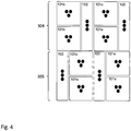
- Fig. 4 shows another schematic diagram of first dedicated pixels 101x and second dedicated pixels 102. Since the dedicated pixels 101x may be identical the same reference sign is used for all first dedicated pixels 101x. The same applies to the two second dedicated pixels 102. However, the pixels with different or rotated arrangements of the light sources 101aR, 101bR, 101cR, 101dR, 101aG, 101bG, 101cG, 101dG, 101aB, 101bB, 101cB, 101dB, 102R, 102G, 102B of Fig. 1 may also be used.
- the first dedicated pixels 101x and the second dedicated pixels 102 are shifted between a first line 304 or row and a second 305 line or row.
- the first line 304 starts with the arrangement shown in Figs. 1 and 2 and comprises a further second dedicated pixel 102 at the end.
- the second line 305 in contrast starts with a second dedicated pixel 102 and then comprises the arrangement of Figs. 1 and 2 next to the second dedicated pixel 102. This means the second line 305 is shifted by the width of a second dedicated pixel 102 in contrast to the first line 304.
- the configuration shown in Fig. 4 can e.g. be used to form a complete panel for a display, as e.g. shown in Fig. 6 .
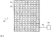
- Fig. 5 shows a schematic diagram of a display device 400.
- the display device 400 comprises a plurality of lines 404, 405 (more indicated by three dots).
- a controller 402 is provided to control the single pixels, dedicated and virtual, of the display 400 and provides according color image data 403.
- every line 404, 405 comprises the same arrangement of pixels, as e.g. shown in Fig. 3 . That means that the first dedicated pixels and the second dedicated pixels are arranged in the same position in every line 404, 405 of the display device 400, e.g. in vertical lines.
- Fig. 6 shows an alternative schematic diagram of a display device 500.
- the lines alternatingly start either with two first dedicated pixels 101x or with a second dedicated pixel 102, as e.g. shown in Fig. 4 .
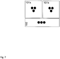
- Fig. 7 shows another schematic diagram of first dedicated pixels 101x and a second dedicated pixel 102.
- Fig. 7 two first dedicated pixels 101x are provided horizontally next to each other, again with a small distance in between.
- the second dedicated pixel 102 is horizontally positioned below the two first dedicated pixels 101x.
- Fig. 7 is an alternative arrangement to the arrangement of Figs. 1 and 2 and can be used in applications, where a rotation of the dedicated pixels 101x, 102 may be beneficial.
- Fig. 8 shows another schematic diagram of a first dedicated pixel 101 and a second dedicated pixel 102.
- the first dedicated pixel is square shaped and has a predetermined edge length 701.
- the second dedicated pixel 102 is rectangular shaped and has a horizontal edge length 702 and a vertical edge length 703.
- the edge length 701 of the first dedicated pixel 101 is approximately half the length of the vertical edge length 703 of the second dedicated pixel 702 and double the length of the horizontal edge length 702 of the second dedicated pixel 702.
- the first dedicated pixel 101 may have an edge length 701 of 50 micrometers to 5 millimeters, especially 100 micrometers to 3 millimeters, and more especially 600 micrometers.
- the second dedicated pixel 102 may have a vertical edge length 703 of 10 micrometers to 10 millimeters, especially 20 micrometers to 6 millimeters, and more especially 1 millimeter, and a horizontal edge length 703 of 10 micrometers to 10 millimeters, especially 30 micrometers to 3 millimeters, and more especially 300 micrometers.
- Fig. 9 shows a flow diagram of an embodiment of an assembly method for a display device 400, 500 for displaying color image data 403, 503.
- the reference signs used in conjunction with Figs. 1 - 6 will be used in the description of Fig. 9 .
- the assembly method comprises providing S1 a plurality of first dedicated pixels 101a, 101b, 101c, 101d, 101x comprising a square shape, and providing S2 a plurality of second dedicated pixels 102 comprising a rectangular shape.
- first dedicated pixels 101a, 101b, 101c, 101d, 101x and the second dedicated pixels 102 are arranged S3 interlaced to form a display surface, wherein each first dedicated pixel 101a, 101b, 101c, 101d, 101x and each second dedicated pixel 102 comprises exactly three light sources of different colors.
- the assembly method can further comprise providing each first dedicated pixel 101a, 101b, 101c, 101d, 101x and each second dedicated pixel 102 with one red light source 101aR, 101bR, 101cR, 101dR, 102R and one green light source 101aG, 101bG, 101cG, 101dG, 102G and one blue light source 101aB, 101bB, 101cB, 101dB, 102B.
- first dedicated pixels 101a, 101b, 101c, 101d, 101x and/or the second dedicated pixels 102 can be provided as integrated surface mount light emitting diodes, SMD-LEDs, with three light sources or as three discrete light emitting diodes, LEDs, wherein the discrete light emitting diodes comprise surface mounted devices, SMD, or through-hole devices.
- two of the first dedicated pixels 101a, 101b, 101c, 101d, 101x can, when vertically positioned adjacent to each other, have the height of one vertically positioned second dedicated pixel 102.
- arranging may comprise positioning two of the first dedicated pixels 101a, 101b, 101c, 101d, 101x vertically positioned adjacent to each other horizontally next to one vertically positioned second dedicated pixel 102.
- Arranging may further comprise providing a pitch between the first dedicated pixels 101a, 101b, 101c, 101d, 101x and/or the second dedicated pixels 102 arranged next to each other that is smaller than five times or four times or three times the edge size of the respective first dedicated pixels 101a, 101b, 101c, 101d, 101x and/or second dedicated pixels 102.
- Arranging may further comprise line-wise arranging the first dedicated pixels 101a, 101b, 101c, 101d, 101x and the second dedicated pixels 102, wherein all the lines 304, 305, 404, 405, 504, 505 may start with two of the first dedicated pixels 101a, 101b, 101c, 101 d, 101x vertically positioned adjacent to each other or with one of the second dedicated pixels 102. Further the lines 304, 305, 404, 405, 504, 505 may alternatingly start with two of the first dedicated pixels 101a, 101b, 101c, 101d, 101x vertically positioned adjacent to each other and one of the second dedicated pixels 102.
- providing may comprise providing the first dedicated pixels 101a, 101b, 101c, 101d, 101x with an edge length of 50 micrometers to 5 millimeters, especially 100 micrometers to 3 millimeters, and more especially 600 micrometers, and providing the second dedicated pixels 102 with a vertical edge length of 10 micrometers to 10 millimeters, especially 20 micrometers to 6 millimeters, and more especially 1 millimeter, and providing the second dedicated pixels 102 with a horizontal edge length of 10 micrometers to 10 millimeters, especially 30 micrometers to 3 millimeters, and more especially 300 micrometers.
- the three light sources of the first dedicated pixels 101a, 101b, 101c, 101d, 101x may be provided arranged in a triangle shape. Further, the three light sources in the second dedicated pixels 102 may be arranged in a line arrangement.
- the present invention provides a display device (400, 500) for displaying color image data (403, 503), the display device (400, 500) comprising a plurality of first dedicated pixels (101a, 101b, 101c, 101d, 101x) comprising a square shape, and a plurality of second dedicated pixels (102) comprising a rectangular shape, wherein the first dedicated pixels (101a, 101b, 101c, 101d, 101x) and the second dedicated pixels (102) are arranged interlaced to form a display surface, and wherein each first dedicated pixel (101a, 101b, 101c, 101d, 101x) and each second dedicated pixel (102) comprises exactly three light sources of different colors. Further, the present invention provides a respective assembly method.
Landscapes
- Engineering & Computer Science (AREA)
- Physics & Mathematics (AREA)
- General Physics & Mathematics (AREA)
- Theoretical Computer Science (AREA)
- Computer Hardware Design (AREA)
- Devices For Indicating Variable Information By Combining Individual Elements (AREA)
- Control Of Indicators Other Than Cathode Ray Tubes (AREA)
- Led Device Packages (AREA)
Abstract
Description
- The invention relates to a display device and manufacturing method for a display device
- Although applicable to any system that uses single light sources such as microLED (µLED) displays to display image data, the present invention will be described in combination with LED displays that use RGB LEDs to display image data, and more specifically in combination with inorganic RGB SMD LED displays.
- LED displays may use single color DIP LEDs or RGB LEDs to form a single pixel and a plurality of pixels to display an image. With this arrangement the resolution of the display is limited by the size of the single color LEDs.
- There exist displays that use discrete through-hole or SMD LEDs in different color to provide a pixel. Usually one pixel will be built up of one discrete red LED, one discrete green LED and one discrete blue LED. Such pixels may be called 1R1G1B pixels.
- However, to increase the resolution of LED displays, the technique of virtual pixels has been introduced, where one virtual pixel is formed of two adjacent pixels. However, this technique can only be used with symmetrical pixels. The pixels for use with virtual pixels will therefore comprise two discrete red LEDs, one discrete green LED and one discrete blue LED. Such pixels may be called 2R1G1B pixel. However, such 2R1G1B pixel are non-standard pixels as compared to 1R1G1B pixels and need to be specifically produced. On a virtual pixel LED screen, the red, green and blue data taken from the four pixels of the image displayed are mapped to light the red, green and blue LEDs of the physical pixel on the screen. Therefore, theoretically the resolution will be four times, two time vertically and two time horizontally, the resolution of a real pixel technology LED display.
- Accordingly, there is a need for providing high resolution displays with standard building blocks.
- Document
WO 2014 / 197 252 A2 discloses a display array that may include a plurality of multifunctional pixels. Each multifunctional pixel can include a red display area, a green display area, and a blue display area. - The present invention provides a display device with the features of claim 1 and a corresponding method with the features of claim 10.
- Consequently, a display device for displaying color image data comprises a plurality of first dedicated pixels comprising a square shape, in a top view, i.e. viewed from the direction of main light emission of the pixel or the single light sources of the pixel, a plurality of second dedicated pixels comprising a rectangular shape, also in a top view, i.e. viewed from the direction of main light emission of the pixel or the single light sources of the pixel, wherein the first dedicated pixels and the second dedicated pixels are arranged interlaced to form a display surface, and wherein each first dedicated pixel and each second dedicated pixel comprises exactly three light sources of different colors.
- Further, an assembly method for a display device for displaying color image data comprises providing a plurality of first dedicated pixels comprising a square shape, and providing a plurality of second dedicated pixels comprising a rectangular shape, and arranging the first dedicated pixels and the second dedicated pixels interlaced to form a display surface, wherein each first dedicated pixel and each second dedicated pixel comprises exactly three light sources of different colors.
- The display device of the present invention combines square shaped and rectangular shaped pixels of only three different colors. Every single pixel therefore only comprises three light sources. Such pixels are easy to manufacture and easy to interface, since e.g. only three signal lines and one common ground is needed per pixel. Alternatively one common input and three switched ground connections can be provided.
- Common display controllers use virtual pixels to increase the resolution of a display. However, these virtual pixel controllers require pixels that have two red light sources, so called 2R1G1B light sources.
- However, the interlaced arrangement of the single pixels in the present invention allows forming virtual pixels using at least two light sources of different colors of at least one first dedicated pixel and one light source of another color of at least one second dedicated pixel. The present invention therefore does neither need two red light sources nor any complex interpolation algorithms to increase the resolution of the display but can be used with virtual pixel algorithms that require less computing power than interpolation algorithms.
- Known LED displays with all rectangular or all square package RGB LEDs are not efficient at fine pitch applications. For example with LED sizes of 1.2mm x 1.2mm and pitch sizes smaller than 2mm virtual pixels cannot be efficiently used. The same applies for LEDs of size 0.6mm x 0.6mm and a pitch size smaller than 1mm solution. In general the present patent application is especially useful if the LED sizes are smaller than 1mm and the pitch size is smaller than three times the RGB LED size. However, the present patent application can be use with any other size of LEDs.
- Therefore, the present invention further allows increasing the resolution of a display device with three colored light sources per pixel, without the need to add a fourth light source to each pixel.
- Further embodiments of the present invention are subject of the further subclaims and of the following description, referring to the drawings.
- In another embodiment, each first dedicated pixel and each second dedicated pixel can comprise one red light source and one green light source and one blue light source. Using red, green and blue, also called RGB in this context, as colors of the light sources allows using standard colors that can be combined with any type of display controller without requiring any amendments on the side of the display controller. Such a display controller can e.g. be comprised in the display device and comprise algorithms to control the single dedicated pixels according to received image data. Further, such a display controller can also be configured to control virtual pixels in the display device. In order to control virtual pixels in the display device, the controller can use single color light sources of adjacent dedicated pixels to form a new virtual pixel comprising one light source of every color or more, e.g. one or two red light sources and one green light source and one blue light source.
- In another embodiment, the first dedicated pixels and the second dedicated pixels can comprise integrated surface mount light emitting diodes with three light sources, e.g. SMD LEDs with single red, green and blue colored diodes in one SMD housing, or three discrete light emitting diodes, e.g. each with a different color, e.g. red, green and blue, wherein the discrete light emitting diodes comprise surface mounted devices, like SMD LEDs, or through-hole devices. The present invention can be used with any type of three color LED arrangement, especially RGB arrangements. SMD RGB LEDs will provide very compact pixels and therefore allow for a very fine pitch and a tight assembly. The term pitch in this context refers to the distance between two single pixels.
- In another embodiment, two of the first dedicated pixels vertically positioned adjacent to or on top of each other can have the height of one vertically positioned second dedicated pixel. Further, in the interlaced arrangement two of the first dedicated pixels vertically positioned adjacent to each other can be horizontally arranged next to one vertically positioned second dedicated pixel. In another embodiment, the pitch between the first dedicated pixels and/or the second dedicated pixels arranged next to each other can be smaller than five times or four times or three times the edge size of the respective first dedicated pixels and/or second dedicated pixels. Two of the first dedicated pixels stacked on top of each other can be as high as a single second dedicated pixel. That means that two vertically stacked first dedicated pixels and one second dedicated pixel next to each other can form a rectangular arrangement of three pixels. These can then flexibly be arranged to build up the complete surface of the display device.
- In another embodiment, the display device can comprise line-wise arrangements of the first dedicated pixels and the second dedicated pixels. In the line wise arrangements the pixels can be arranged e.g. with the above mentioned rectangular arrangement of three pixels. The lines can be horizontal or vertical lines.
- In another embodiment, all the lines can start with two of the first dedicated pixels vertically positioned adjacent to each other or with one of the second dedicated pixels. This arrangement provides for identical line arrangements of the first and second dedicated pixels. Therefore, easy manufacturing of the display device is possible.
- In another embodiment, the lines can alternatingly start with two of the first dedicated pixels vertically positioned adjacent to each other or one of the second dedicated pixels. This arrangement provides slightly shifted pixels from one line to the next and therefore provides a smoothed image.
- In another embodiment, the first dedicated pixels can comprise an edge length of 50 micrometers to 5 millimeters, especially 100 micrometers to 3 millimeters, and more especially 600 micrometers. In addition or as alternative, the second dedicated pixels can comprise a vertical edge length of 10 micrometers to 10 millimeters, especially 20 micrometers to 6 millimeters, and more especially 1 millimeter. Further as an alternative or in addition, the second dedicated pixels can comprise a horizontal edge length of 10 micrometers to 10 millimeters, especially 30 micrometers to 3 millimeters, and more especially 300 micrometers. The present invention can especially be used with very fine pitch and in very tight assemblies. In contrast systems in the prior art can only use SMD RGB LEDs with virtual pixels, and sometimes only with complex interpolations, if the pitch size is much greater than the LED size.
- In another embodiment, in the first dedicated pixels the three light sources can be arranged in a triangle shape, e.g. with one light source being arranged on each one of the corners of the triangle. In addition or as alternative in the second dedicated pixels the three light sources can be arranged in a line arrangement, e.g. a horizontal line or a vertical line.
- It is understood that the orientation of the triangle or the line can vary from application to application. For example a tip of the triangle can be positioned in the top center position or the triangle can be rotated in any angle from this position. The same applies to the line arrangement. The three light sources can e.g. be positioned on a vertical line, a horizontal line or a rotated line with any rotation angle.
- For a more complete understanding of the present invention and advantages thereof, reference is now made to the following description taken in conjunction with the accompanying drawings. The invention is explained in more detail below using exemplary embodiments which are specified in the schematic figures of the enclosed drawings, in which:
-
Fig. 1 shows a schematic diagram of first and second dedicated pixels according to an embodiment of the present invention; -
Fig. 2 shows another schematic diagram of first and second dedicated pixels according to an embodiment of the present invention; -
Fig. 3 shows another schematic diagram of first and second dedicated pixels according to an embodiment of the present invention; -
Fig. 4 shows another schematic diagram of first and second dedicated pixels according to an embodiment of the present invention; -
Fig. 5 shows a schematic diagram of an embodiment of a display device according to the present invention; -
Fig. 6 shows a schematic diagram of another embodiment of a display device according to the present invention; -
Fig. 7 shows another schematic diagram of first and second dedicated pixels according to an embodiment of the present invention; -
Fig. 8 shows another schematic diagram of first and second dedicated pixels according to an embodiment of the present invention; and -
Fig. 9 shows a flow diagram of an embodiment of an assembly method according to the present invention. - In the figures like reference signs denote like elements unless stated otherwise.
-
Fig. 1 shows a schematic diagram of firstdedicated pixels dedicated pixel 102. - The first
dedicated pixels dedicated pixel 102 comprises a rectangular shape, wherein the vertical side of the rectangular shape is as long as twice the length of a side of the firstdedicated pixels dedicated pixels -
Fig. 1 shows four firstdedicated pixels dedicated pixel 102. The four firstdedicated pixels dedicated pixels dedicated pixel 102. - In the arrangement of
Fig. 1 every firstdedicated pixel dedicated pixel 102 comprises three light sources, for example LEDs, of different colors. The firstdedicated pixels dedicated pixels - The second
dedicated pixel 102 also comprises three light sources, e.g. LEDs, onered light source 102R, onegreen light source 102G, and one bluelight source 102B, which are arranged on a vertical line from bottom to top. - In the two first
dedicated pixels - In the two first
dedicated pixels - It is understood, that the above described arrangement of single light sources 101aR, 101bR, 101cR, 101dR, 101aG, 101bG, 101cG, 101dG, 101aB, 101bB, 101cB, 101dB, 102R, 102G, 102B in the first
dedicated pixels dedicated pixel 102 is just exemplary and other arrangements can also be used. - The arrangement of the first
dedicated pixels dedicated pixel 102 ofFig. 1 allows providing a plurality of virtual pixels in addition to the presented firstdedicated pixels dedicated pixel 102. -
Fig. 2 therefore shows the same arrangement ofpixels Fig. 1 . The reference signs of the single light sources 101aR, 101bR, 101cR, 101dR, 101aG, 101bG, 101cG, 101dG, 101aB, 101bB, 101cB, 101dB, 102R, 102G, 102B have been omitted for sake of clarity, however the reference signs ofFig. 1 apply.
InFig. 2 , the possible combinations of light sources 101aR, 101bR, 101cR, 101dR, 101aG, 101bG, 101cG, 101dG, 101aB, 101bB, 101cB, 101dB, 102R, 102G, 102B to form a pixel of the displayed image are each shown by a line delineating their respective circumference.Real pixels dedicated pixel - The possible
virtual pixels virtual pixel 206 comprises the red light source 101aR and the blue light source 101aB of the top left firstdedicated pixel 101a and thegreen light source 102G of the seconddedicated pixel 102. The secondvirtual pixel 207 comprises the blue light source 101bB and the green light source 101bG of the lower left firstdedicated pixel 101b and thered light source 102R of the seconddedicated pixel 102. The thirdvirtual pixel 208 comprises the red light source 101cR and the blue light source 101cB of the upper right firstdedicated pixel 101c and thegreen light source 102G of the seconddedicated pixel 102. The fourthvirtual pixel 209 comprises the blue light source 101dB and the green light source 101dG of the lower right firstdedicated pixel 101d and thered light source 102G of the seconddedicated pixel 102. - The shown arrangement of first
dedicated pixels dedicated pixel 102 therefore allows providing a total of 9 pixels out of five real ordedicated pixels - Alternative arrangements are also possible. The virtual pixels can e.g. use all three light sources of the respective first
dedicated pixel red light source 102R of the seconddedicated pixel 102. - The first
dedicated pixels dedicated pixels 102 can comprise a vertical edge length of 10 micrometers to 10 millimeters, especially 20 micrometers to 6 millimeters, and more especially 1 millimeter. Further the seconddedicated pixels 102 can comprise a horizontal edge length of 10 micrometers to 10 millimeters, especially 30 micrometers to 3 millimeters, and more especially 300 micrometers
Fig. 3 shows another schematic diagram of firstdedicated pixels 101x and seconddedicated pixels 102. Since thededicated pixels 101x may be identical the same reference sign is used for all firstdedicated pixels 101x. The same applies to the two seconddedicated pixels 102. However, the pixels with different or rotated arrangements of the light sources 101aR, 101bR, 101cR, 101dR, 101aG, 101bG, 101cG, 101dG, 101aB, 101bB, 101cB, 101dB, 102R, 102G, 102B ofFig. 1 may also be used. - In
Fig. 3 the arrangement ofFigs. 1 and2 is doubled, i.e. provided twice, and the two arrangements are provided one vertically over the other. The configuration shown inFig. 3 can e.g. be used to form a complete panel for a display, as e.g. shown inFig. 5 . -
Fig. 4 shows another schematic diagram of firstdedicated pixels 101x and seconddedicated pixels 102. Since thededicated pixels 101x may be identical the same reference sign is used for all firstdedicated pixels 101x. The same applies to the two seconddedicated pixels 102. However, the pixels with different or rotated arrangements of the light sources 101aR, 101bR, 101cR, 101dR, 101aG, 101bG, 101cG, 101dG, 101aB, 101bB, 101cB, 101dB, 102R, 102G, 102B ofFig. 1 may also be used. - In the arrangement of
Fig. 4 the firstdedicated pixels 101x and the seconddedicated pixels 102 are shifted between afirst line 304 or row and a second 305 line or row. Thefirst line 304 starts with the arrangement shown inFigs. 1 and2 and comprises a further seconddedicated pixel 102 at the end. Thesecond line 305 in contrast starts with a seconddedicated pixel 102 and then comprises the arrangement ofFigs. 1 and2 next to the seconddedicated pixel 102. This means thesecond line 305 is shifted by the width of a seconddedicated pixel 102 in contrast to thefirst line 304. The configuration shown inFig. 4 can e.g. be used to form a complete panel for a display, as e.g. shown inFig. 6 . -
Fig. 5 shows a schematic diagram of adisplay device 400. Thedisplay device 400 comprises a plurality oflines 404, 405 (more indicated by three dots). Acontroller 402 is provided to control the single pixels, dedicated and virtual, of thedisplay 400 and provides accordingcolor image data 403. - In the
display device 400 everyline Fig. 3 . That means that the first dedicated pixels and the second dedicated pixels are arranged in the same position in everyline display device 400, e.g. in vertical lines. -
Fig. 6 shows an alternative schematic diagram of a display device 500. In contrast to thedisplay device 400 in the display device 500 the lines alternatingly start either with two firstdedicated pixels 101x or with a seconddedicated pixel 102, as e.g. shown inFig. 4 . - It is understood, that in the
display device 400 and the display device 500 the arrangements ofFigs. 3 and4 can also be used vertically instead of horizontally, i.e. rotated about 90°. Thedisplay device 400 and the display device 500 would then instead of lines comprise columns. -
Fig. 7 shows another schematic diagram of firstdedicated pixels 101x and a seconddedicated pixel 102. - In
Fig. 7 two firstdedicated pixels 101x are provided horizontally next to each other, again with a small distance in between. The seconddedicated pixel 102 is horizontally positioned below the two firstdedicated pixels 101x. - The arrangement in
Fig. 7 is an alternative arrangement to the arrangement ofFigs. 1 and2 and can be used in applications, where a rotation of thededicated pixels -
Fig. 8 shows another schematic diagram of a firstdedicated pixel 101 and a seconddedicated pixel 102. The first dedicated pixel is square shaped and has apredetermined edge length 701. The seconddedicated pixel 102 is rectangular shaped and has ahorizontal edge length 702 and avertical edge length 703. - The
edge length 701 of the firstdedicated pixel 101 is approximately half the length of thevertical edge length 703 of the seconddedicated pixel 702 and double the length of thehorizontal edge length 702 of the seconddedicated pixel 702. - In general, the first
dedicated pixel 101 may have anedge length 701 of 50 micrometers to 5 millimeters, especially 100 micrometers to 3 millimeters, and more especially 600 micrometers. The seconddedicated pixel 102 may have avertical edge length 703 of 10 micrometers to 10 millimeters, especially 20 micrometers to 6 millimeters, and more especially 1 millimeter, and ahorizontal edge length 703 of 10 micrometers to 10 millimeters, especially 30 micrometers to 3 millimeters, and more especially 300 micrometers. -
Fig. 9 shows a flow diagram of an embodiment of an assembly method for adisplay device 400, 500 for displayingcolor image data Figs. 1 - 6 will be used in the description ofFig. 9 . - The assembly method comprises providing S1 a plurality of first
dedicated pixels dedicated pixels 102 comprising a rectangular shape. - Further, the first
dedicated pixels dedicated pixels 102 are arranged S3 interlaced to form a display surface, wherein each firstdedicated pixel dedicated pixel 102 comprises exactly three light sources of different colors. - The assembly method can further comprise providing each first
dedicated pixel dedicated pixel 102 with one red light source 101aR, 101bR, 101cR, 101dR, 102R and one green light source 101aG, 101bG, 101cG, 101dG, 102G and one blue light source 101aB, 101bB, 101cB, 101dB, 102B. In addition or as an alternative the firstdedicated pixels dedicated pixels 102 can be provided as integrated surface mount light emitting diodes, SMD-LEDs, with three light sources or as three discrete light emitting diodes, LEDs, wherein the discrete light emitting diodes comprise surface mounted devices, SMD, or through-hole devices. - Further, two of the first
dedicated pixels dedicated pixel 102. Further, arranging may comprise positioning two of the firstdedicated pixels dedicated pixel 102. Arranging may further comprise providing a pitch between the firstdedicated pixels dedicated pixels 102 arranged next to each other that is smaller than five times or four times or three times the edge size of the respective firstdedicated pixels dedicated pixels 102. - Arranging may further comprise line-wise arranging the first
dedicated pixels dedicated pixels 102, wherein all thelines dedicated pixels dedicated pixels 102. Further thelines dedicated pixels dedicated pixels 102. - In addition, providing may comprise providing the first
dedicated pixels dedicated pixels 102 with a vertical edge length of 10 micrometers to 10 millimeters, especially 20 micrometers to 6 millimeters, and more especially 1 millimeter, and providing the seconddedicated pixels 102 with a horizontal edge length of 10 micrometers to 10 millimeters, especially 30 micrometers to 3 millimeters, and more especially 300 micrometers. - The three light sources of the first
dedicated pixels dedicated pixels 102 may be arranged in a line arrangement. - Although specific embodiments have been illustrated and described herein, it will be appreciated by those of ordinary skill in the art that a variety of alternate and/or equivalent implementations exist. It should be appreciated that the exemplary embodiment or exemplary embodiments are only examples, and are not intended to limit the scope, applicability, or configuration in any way. Rather, the foregoing summary and detailed description will provide those skilled in the art with a convenient road map for implementing at least one exemplary embodiment, it being understood that various changes may be made in the function and arrangement of elements described in an exemplary embodiment without departing from the scope as set forth in the appended claims and their legal equivalents. Generally, this application is intended to cover any adaptations or variations of the specific embodiments discussed herein.
- The present invention provides a display device (400, 500) for displaying color image data (403, 503), the display device (400, 500) comprising a plurality of first dedicated pixels (101a, 101b, 101c, 101d, 101x) comprising a square shape, and a plurality of second dedicated pixels (102) comprising a rectangular shape, wherein the first dedicated pixels (101a, 101b, 101c, 101d, 101x) and the second dedicated pixels (102) are arranged interlaced to form a display surface, and wherein each first dedicated pixel (101a, 101b, 101c, 101d, 101x) and each second dedicated pixel (102) comprises exactly three light sources of different colors. Further, the present invention provides a respective assembly method.
-
- 400, 500
- display device
- 101a, 101b, 101c, 101d, 101x
- first dedicated pixels
- 102
- second dedicated pixels
- 101aR, 101bR, 101cR, 101dR, 102R
- red light source
- 101aG, 101bG, 101cG, 101dG, 102G
- green light source
- 101aB, 101bB, 101cB, 101dB, 102B
- blue light source
- 201, 202, 203, 204, 205
- real pixel
- 206, 207, 208, 209
- virtual pixel
- 304, 305
- line
- 402, 502
- controller
- 403, 503
- color image data
- 404, 405
- line
- 504, 505
- line
- 701, 702, 703
- edge length
- S1 - S3
- method steps
Claims (15)
- Display device (400, 500) for displaying color image data (403, 503), the display device (400, 500) comprising:a plurality of first dedicated pixels (101a, 101b, 101c, 101d, 101x) comprising a square shape, anda plurality of second dedicated pixels (102) comprising a rectangular shape,wherein the first dedicated pixels (101a, 101b, 101c, 101d, 101x) and the second dedicated pixels (102) are arranged interlaced to form a display surface, andwherein each first dedicated pixel (101a, 101b, 101c, 101d, 101x) and each second dedicated pixel (102) comprises exactly three light sources of different colors.
- Display device (400, 500) according to claim 1, wherein each first dedicated pixel (101a, 101b, 101c, 101d, 101x) and each second dedicated pixel (102) comprises one red light source (101aR, 101bR, 101cR, 101dR, 102R) and one green light source (101aG, 101bG, 101cG, 101dG, 102G) and one blue light source (101aB, 101bB, 101cB, 101dB, 102B).
- Display device (400, 500) according to any one of the preceding claims, wherein the first dedicated pixels (101a, 101b, 101c, 101d, 101x) and the second dedicated pixels (102) comprise integrated surface mount light emitting diodes with three light sources or three discrete light emitting diodes, wherein the discrete light emitting diodes comprise surface mounted devices or through-hole devices.
- Display device (400, 500) according to any one of the preceding claims, wherein two of the first dedicated pixels (101a, 101b, 101c, 101d, 101x) vertically positioned adjacent to each other have the height of one vertically positioned second dedicated pixel (102), and wherein in the interlaced arrangement two of the first dedicated pixels (101a, 101b, 101c, 101d, 101x) vertically positioned adjacent to each other are horizontally arranged next to one vertically positioned second dedicated pixel (102), and
especially wherein the pitch between the first dedicated pixels (101a, 101b, 101c, 101d, 101x) and/or the second dedicated pixels (102) arranged next to each other is smaller than five times or four times or three times the edge size of the respective first dedicated pixels (101a, 101b, 101c, 101d, 101x) and/or second dedicated pixels (102). - Display device (400, 500) according to any one of the preceding claims, comprising line-wise arrangements of the first dedicated pixels (101a, 101b, 101c, 101d, 101x) and the second dedicated pixels (102).
- Display device (400, 500) according to claim 5, wherein all the lines (304, 305, 404, 405, 504, 505) start with two of the first dedicated pixels (101a, 101b, 101c, 101d, 101x) vertically positioned adjacent to each other or wherein all the lines (304, 305, 404, 405, 504, 505) start with one of the second dedicated pixels (102).
- Display device (400, 500) according to claim 5, wherein the lines (304, 305, 404, 405, 504, 505) alternatingly start with two of the first dedicated pixels (101a, 101b, 101c, 101d, 101x) vertically positioned adjacent to each other or one of the second dedicated pixels (102).
- Display device (400, 500) according to any one of the preceding claims, wherein the first dedicated pixels (101a, 101b, 101c, 101d, 101x) comprise an edge length (701) of 50 micrometers to 5 millimeters, especially 100 micrometers to 3 millimeters, and more especially 600 micrometers, and
wherein the second dedicated pixels (102) comprise a vertical edge length (703) of 10 micrometers to 10 millimeters, especially 20 micrometers to 6 millimeters, and more especially 1 millimeter, and
wherein the second dedicated pixels (102) comprise a horizontal edge length (703) of 10 micrometers to 10 millimeters, especially 30 micrometers to 3 millimeters, and more especially 300 micrometers. - Display device (400, 500) according to any one of the preceding claims, wherein in the first dedicated pixels (101a, 101b, 101c, 101d, 101x) the three light sources are arranged in a triangle shape, and/or
wherein in the second dedicated pixels (102) the three light sources are arranged in a line arrangement. - Assembly method for a display device (400, 500) for displaying color image data (403, 503), the assembly method comprising:providing (S1) a plurality of first dedicated pixels (101a, 101b, 101c, 101d, 101x) comprising a square shape, andproviding (S2) a plurality of second dedicated pixels (102) comprising a rectangular shape,arranging (S3) the first dedicated pixels (101a, 101b, 101c, 101d, 101x) and the second dedicated pixels (102) interlaced to form a display surface,wherein each first dedicated pixel (101a, 101b, 101c, 101d, 101x) and each second dedicated pixel (102) comprises exactly three light sources of different colors.
- Assembly method according to claim 1, comprising providing each first dedicated pixel (101a, 101b, 101c, 101d, 101x) and each second dedicated pixel (102) with one red light source (101aR, 101bR, 101cR, 101dR, 102R) and one green light source (101aG, 101bG, 101cG, 101dG, 102G) and one blue light source (101aB, 101bB, 101cB, 101dB, 102B); and/or
providing the first dedicated pixels (101a, 101b, 101c, 101d, 101x) and/or the second dedicated pixels (102) as integrated surface mount light emitting diodes with three light sources or as three discrete light emitting diodes, wherein the discrete light emitting diodes comprise surface mounted devices or through-hole devices. - Assembly method according to any one of the preceding claims 10 and 11, wherein two of the first dedicated pixels (101a, 101b, 101c, 101d, 101x) vertically positioned adjacent to each other have the height of one vertically positioned second dedicated pixel (102), and wherein arranging comprises positioning two of the first dedicated pixels (101a, 101b, 101c, 101d, 101x) vertically positioned adjacent to each other horizontally next to one vertically positioned second dedicated pixel (102), and
wherein arranging especially comprises providing a pitch between the first dedicated pixels (101a, 101b, 101c, 101d, 101x) and/or the second dedicated pixels (102) arranged next to each other that is smaller than five times or four times or three times the edge size of the respective first dedicated pixels (101a, 101b, 101c, 101d, 101x) and/or second dedicated pixels (102). - Assembly method according to any one of the preceding claims 10 to 12, wherein arranging comprises line-wise arranging the first dedicated pixels (101a, 101b, 101c, 101d, 101x) and the second dedicated pixels (102), especially wherein all the lines (304, 305, 404, 405, 504, 505) start with two of the first dedicated pixels (101a, 101b, 101c, 101d, 101x) vertically positioned adjacent to each other or wherein all the lines (304, 305, 404, 405, 504, 505) start with one of the second dedicated pixels (102) or wherein the lines (304, 305, 404, 405, 504, 505) alternatingly start with two of the first dedicated pixels (101a, 101b, 101c, 101d, 101x) vertically positioned adjacent to each other and one of the second dedicated pixels (102).
- Assembly method according to any one of the preceding claims, wherein providing comprises providing the first dedicated pixels (101a, 101b, 101c, 101d, 101x) with an edge length (701) of 50 micrometers to 5 millimeters, especially 100 micrometers to 3 millimeters, and more especially 600 micrometers, and
wherein providing comprises providing the second dedicated pixels (102) with a vertical edge length (703) of 10 micrometers to 10 millimeters, especially 20 micrometers to 6 millimeters, and more especially 1 millimeter, and
wherein providing comprises providing the second dedicated pixels (102) with a horizontal edge length (702) of 10 micrometers to 10 millimeters, especially 30 micrometers to 3 millimeters, and more especially 300 micrometers. - Assembly method according to any one of the preceding claims, providing comprises providing the three light sources of the first dedicated pixels (101a, 101b, 101c, 101d, 101x) arranged in a triangle shape, and/or
providing comprises providing the three light sources in the second dedicated pixels (102) arranged in a line arrangement.
Priority Applications (7)
| Application Number | Priority Date | Filing Date | Title |
|---|---|---|---|
| EP16206859.7A EP3343544B1 (en) | 2016-12-28 | 2016-12-28 | Method for a display device |
| TR2017/02847A TR201702847A2 (en) | 2016-12-28 | 2017-02-24 | METHOD FOR AN IMAGE DEVICE |
| US16/474,947 US10867545B2 (en) | 2016-12-28 | 2017-09-21 | Method for a display device |
| PCT/EP2017/073908 WO2018121893A1 (en) | 2016-12-28 | 2017-09-21 | Method for a display device |
| KR1020197020041A KR102451214B1 (en) | 2016-12-28 | 2017-09-21 | Methods for display devices |
| CN201780087388.5A CN110337684B (en) | 2016-12-28 | 2017-09-21 | Method for display device |
| JP2019535281A JP7062671B2 (en) | 2016-12-28 | 2017-09-21 | Display device and assembly method |
Applications Claiming Priority (1)
| Application Number | Priority Date | Filing Date | Title |
|---|---|---|---|
| EP16206859.7A EP3343544B1 (en) | 2016-12-28 | 2016-12-28 | Method for a display device |
Publications (2)
| Publication Number | Publication Date |
|---|---|
| EP3343544A1 true EP3343544A1 (en) | 2018-07-04 |
| EP3343544B1 EP3343544B1 (en) | 2022-06-15 |
Family
ID=57799496
Family Applications (1)
| Application Number | Title | Priority Date | Filing Date |
|---|---|---|---|
| EP16206859.7A Active EP3343544B1 (en) | 2016-12-28 | 2016-12-28 | Method for a display device |
Country Status (7)
| Country | Link |
|---|---|
| US (1) | US10867545B2 (en) |
| EP (1) | EP3343544B1 (en) |
| JP (1) | JP7062671B2 (en) |
| KR (1) | KR102451214B1 (en) |
| CN (1) | CN110337684B (en) |
| TR (1) | TR201702847A2 (en) |
| WO (1) | WO2018121893A1 (en) |
Cited By (1)
| Publication number | Priority date | Publication date | Assignee | Title |
|---|---|---|---|---|
| CN110120188A (en) * | 2019-03-31 | 2019-08-13 | 深圳市亮彩科技有限公司 | A kind of LED display pixel arrangements for being suitable for any angle and showing |
Families Citing this family (17)
| Publication number | Priority date | Publication date | Assignee | Title |
|---|---|---|---|---|
| US11233096B2 (en) | 2016-02-18 | 2022-01-25 | Boe Technology Group Co., Ltd. | Pixel arrangement structure and driving method thereof, display substrate and display device |
| US11747531B2 (en) | 2016-02-18 | 2023-09-05 | Chengdu Boe Optoelectronics Technology Co., Ltd. | Display substrate, fine metal mask set and manufacturing method thereof |
| CN111326121B (en) * | 2018-12-13 | 2021-11-16 | 京东方科技集团股份有限公司 | Driving method, driving chip, display device and storage medium |
| US11448807B2 (en) | 2016-02-18 | 2022-09-20 | Chengdu Boe Optoelectronics Technology Co., Ltd. | Display substrate, fine metal mask set and manufacturing method thereof |
| CN110137213B (en) | 2018-02-09 | 2025-03-25 | 京东方科技集团股份有限公司 | Pixel arrangement structure and display method thereof, and display substrate |
| CN110137215B (en) | 2018-02-09 | 2025-01-14 | 京东方科技集团股份有限公司 | Pixel arrangement structure, display substrate and display device |
| CN110133919B (en) | 2018-02-09 | 2024-09-10 | 京东方科技集团股份有限公司 | Display substrate and display device |
| WO2021016946A1 (en) | 2019-07-31 | 2021-02-04 | 京东方科技集团股份有限公司 | Display substrate and preparation method therefor, display panel, and display apparatus |
| US11574960B2 (en) | 2018-02-09 | 2023-02-07 | Boe Technology Group Co., Ltd. | Pixel arrangement structure, display substrate, display device and mask plate group |
| US11088121B2 (en) * | 2019-02-13 | 2021-08-10 | X Display Company Technology Limited | Printed LED arrays with large-scale uniformity |
| KR102866754B1 (en) | 2019-03-04 | 2025-09-30 | 삼성디스플레이 주식회사 | Carrier, apparatus for manufacturing a display apparatus having the same and method for manufacturing a display apparatus |
| EP4006982B1 (en) | 2019-07-31 | 2026-07-22 | BOE Technology Group Co., Ltd. | Display substrate and display device |
| CN110570774A (en) * | 2019-08-09 | 2019-12-13 | 武汉华星光电半导体显示技术有限公司 | Display panel and display device |
| US11557635B2 (en) | 2019-12-10 | 2023-01-17 | Samsung Display Co., Ltd. | Display device, mask assembly, and apparatus for manufacturing the display device |
| EP4750293A2 (en) | 2019-12-10 | 2026-05-27 | Samsung Display Co., Ltd. | Display device, mask assembly, and apparatus for manufacturing display device |
| US11908881B2 (en) | 2020-01-21 | 2024-02-20 | Seoul Viosys Co., Ltd. | LED display apparatus having micro LED module |
| KR102825567B1 (en) | 2020-06-12 | 2025-06-26 | 엘지전자 주식회사 | Display device including semiconductor light emitting element |
Citations (2)
| Publication number | Priority date | Publication date | Assignee | Title |
|---|---|---|---|---|
| WO2014197252A2 (en) | 2013-06-03 | 2014-12-11 | Qualcomm Incorporated | Multifunctional pixel and display |
| WO2016150117A1 (en) * | 2015-03-26 | 2016-09-29 | Boe Technology Group Co., Ltd. | Pixel structure, display panel, and display apparatus |
Family Cites Families (30)
| Publication number | Priority date | Publication date | Assignee | Title |
|---|---|---|---|---|
| TW377429B (en) * | 1998-02-11 | 1999-12-21 | Au Optronics Corp | Method of showing graphics on dot matrix display |
| JP3870807B2 (en) * | 2001-12-20 | 2007-01-24 | ソニー株式会社 | Image display device and manufacturing method thereof |
| JP2005352408A (en) | 2004-06-14 | 2005-12-22 | Sanyo Electric Co Ltd | Display device |
| TWI258721B (en) * | 2004-08-10 | 2006-07-21 | Ind Tech Res Inst | Full-color organic electroluminescence device |
| US7907133B2 (en) * | 2006-04-13 | 2011-03-15 | Daktronics, Inc. | Pixel interleaving configurations for use in high definition electronic sign displays |
| GB2437110B (en) | 2006-04-12 | 2009-01-28 | Cambridge Display Tech Ltd | Optoelectronic display and method of manufacturing the same |
| JP5303834B2 (en) * | 2006-12-19 | 2013-10-02 | 日亜化学工業株式会社 | Light emitting device |
| JP5311779B2 (en) * | 2007-08-21 | 2013-10-09 | シチズン電子株式会社 | LED light emitting device |
| JP5215090B2 (en) * | 2008-02-25 | 2013-06-19 | 三菱電機株式会社 | Image display device and display unit for image display device |
| CN103559838B (en) * | 2008-05-11 | 2016-03-23 | Nlt科技股份有限公司 | The pel array of non-rectangle and there is the display device of this array |
| JP2010206138A (en) * | 2009-03-06 | 2010-09-16 | Nichia Corp | Light emitting device |
| KR20110013691A (en) * | 2009-08-03 | 2011-02-10 | 삼성모바일디스플레이주식회사 | Pixel structure and organic light emitting display device using the same |
| DE102011053000B4 (en) * | 2010-08-27 | 2017-08-17 | Lg Display Co., Ltd. | Organic electroluminescent device |
| US9583034B2 (en) * | 2010-10-15 | 2017-02-28 | Lg Display Co., Ltd. | Subpixel arrangement structure for display device |
| TWI550571B (en) * | 2011-11-09 | 2016-09-21 | 友達光電股份有限公司 | Three-dimension display panel and driving method thereof |
| EP4608107A3 (en) * | 2012-09-13 | 2025-11-05 | Samsung Display Co., Ltd. | Pixel arrangement structure for organic light emitting diode display |
| JP2016512344A (en) * | 2013-03-11 | 2016-04-25 | 深セン市奥拓電子股▲分▼有限公司 | High-resolution LED display and its surface-mount LED combination lamp with ultra fine dot pitch |
| KR102127762B1 (en) * | 2013-10-02 | 2020-06-30 | 삼성디스플레이 주식회사 | Flat panel display device |
| JP6349406B2 (en) * | 2013-11-04 | 2018-06-27 | シェンジェン ユンイング テクノロジー カンパニー リミテッド | Display sub-pixel arrangement and method for rendering the same |
| CN103903524B (en) * | 2014-03-25 | 2016-06-15 | 京东方科技集团股份有限公司 | Display packing |
| CN103903549B (en) * | 2014-03-25 | 2016-08-17 | 京东方科技集团股份有限公司 | Display packing |
| CN104036700B (en) * | 2014-05-30 | 2016-02-03 | 京东方科技集团股份有限公司 | Display panel, display packing and display device |
| CN104299974B (en) * | 2014-09-29 | 2017-02-15 | 京东方科技集团股份有限公司 | Array substrate, mask plate and display device |
| CN104637987A (en) * | 2015-02-06 | 2015-05-20 | 友达光电股份有限公司 | Active matrix organic light emitting display and pixel structure thereof |
| US9837473B2 (en) * | 2015-04-29 | 2017-12-05 | Lg Display Co., Ltd. | Organic light emitting diode display |
| KR102390473B1 (en) * | 2015-06-30 | 2022-04-25 | 엘지디스플레이 주식회사 | Display panel and display device having the same |
| CN108155204B (en) * | 2016-12-02 | 2020-03-17 | 京东方科技集团股份有限公司 | Pixel arrangement structure, display device and mask plate |
| CN108807460B (en) * | 2017-04-28 | 2019-08-23 | 昆山国显光电有限公司 | Dot structure driving method |
| US11152432B1 (en) * | 2017-08-31 | 2021-10-19 | Kunshan Go-Visionox Opto-Electronics Co., Ltd. | Pixel structure, OLED display device and driving method |
| US20190333434A1 (en) * | 2018-04-29 | 2019-10-31 | Mikro Mesa Technology Co., Ltd. | High fill rate display |
-
2016
- 2016-12-28 EP EP16206859.7A patent/EP3343544B1/en active Active
-
2017
- 2017-02-24 TR TR2017/02847A patent/TR201702847A2/en unknown
- 2017-09-21 WO PCT/EP2017/073908 patent/WO2018121893A1/en not_active Ceased
- 2017-09-21 CN CN201780087388.5A patent/CN110337684B/en not_active Expired - Fee Related
- 2017-09-21 KR KR1020197020041A patent/KR102451214B1/en not_active Expired - Fee Related
- 2017-09-21 JP JP2019535281A patent/JP7062671B2/en active Active
- 2017-09-21 US US16/474,947 patent/US10867545B2/en not_active Expired - Fee Related
Patent Citations (2)
| Publication number | Priority date | Publication date | Assignee | Title |
|---|---|---|---|---|
| WO2014197252A2 (en) | 2013-06-03 | 2014-12-11 | Qualcomm Incorporated | Multifunctional pixel and display |
| WO2016150117A1 (en) * | 2015-03-26 | 2016-09-29 | Boe Technology Group Co., Ltd. | Pixel structure, display panel, and display apparatus |
Cited By (1)
| Publication number | Priority date | Publication date | Assignee | Title |
|---|---|---|---|---|
| CN110120188A (en) * | 2019-03-31 | 2019-08-13 | 深圳市亮彩科技有限公司 | A kind of LED display pixel arrangements for being suitable for any angle and showing |
Also Published As
| Publication number | Publication date |
|---|---|
| US20190340970A1 (en) | 2019-11-07 |
| JP7062671B2 (en) | 2022-05-06 |
| KR20190097120A (en) | 2019-08-20 |
| TR201702847A2 (en) | 2018-07-23 |
| CN110337684B (en) | 2023-04-04 |
| US10867545B2 (en) | 2020-12-15 |
| JP2020514792A (en) | 2020-05-21 |
| WO2018121893A1 (en) | 2018-07-05 |
| EP3343544B1 (en) | 2022-06-15 |
| KR102451214B1 (en) | 2022-10-05 |
| CN110337684A (en) | 2019-10-15 |
Similar Documents
| Publication | Publication Date | Title |
|---|---|---|
| US10867545B2 (en) | Method for a display device | |
| EP4044165B1 (en) | Organic light emitting display device | |
| CN205487172U (en) | Display | |
| EP3166098B1 (en) | Pixel array and driving method thereof and display panel | |
| US8130175B1 (en) | Pixel interleaving configurations for use in high definition electronic sign displays | |
| US9799252B2 (en) | Pixel array and driving method thereof, display panel and display device | |
| CN104299561B (en) | Driving method of pixel array | |
| CN104680949B (en) | Pel array, display drive method, display drive apparatus and display device | |
| US10013913B2 (en) | Pixel structure, display substrate and display device | |
| US11004906B2 (en) | Display panel, display apparatus, and mask plate for fabricating display panel | |
| CN109727542B (en) | Special-shaped display screen and display device | |
| EP3678183A1 (en) | Pixel structure, mask and display device | |
| WO2016138714A1 (en) | Display drive method and device, and sampling area generation method and device | |
| TWI524125B (en) | Pixel array | |
| EP3065125A1 (en) | Display panel and display apparatus having the same | |
| US10297182B2 (en) | Pixel array having sub-pixel groups and driving method thereof and display panel | |
| US11730029B2 (en) | Display substrate, light field display apparatus and method for driving the same | |
| CN103995374A (en) | Display panel and display device | |
| CN106097898A (en) | Pel array, display base plate and display device | |
| US20170256232A1 (en) | Pixel structure | |
| CN103984163A (en) | Liquid crystal grating and display equipment | |
| CN107799013A (en) | Display panel, display screen and display device | |
| CN111164758A (en) | Display device for improving edge color cast and television | |
| EP3200176B1 (en) | Image display method and display device | |
| CN109859666B (en) | Pixel arrangement structure, display panel and display device |
Legal Events
| Date | Code | Title | Description |
|---|---|---|---|
| PUAI | Public reference made under article 153(3) epc to a published international application that has entered the european phase |
Free format text: ORIGINAL CODE: 0009012 |
|
| STAA | Information on the status of an ep patent application or granted ep patent |
Free format text: STATUS: THE APPLICATION HAS BEEN PUBLISHED |
|
| AK | Designated contracting states |
Kind code of ref document: A1 Designated state(s): AL AT BE BG CH CY CZ DE DK EE ES FI FR GB GR HR HU IE IS IT LI LT LU LV MC MK MT NL NO PL PT RO RS SE SI SK SM TR |
|
| AX | Request for extension of the european patent |
Extension state: BA ME |
|
| STAA | Information on the status of an ep patent application or granted ep patent |
Free format text: STATUS: REQUEST FOR EXAMINATION WAS MADE |
|
| 17P | Request for examination filed |
Effective date: 20181220 |
|
| RBV | Designated contracting states (corrected) |
Designated state(s): AL AT BE BG CH CY CZ DE DK EE ES FI FR GB GR HR HU IE IS IT LI LT LU LV MC MK MT NL NO PL PT RO RS SE SI SK SM TR |
|
| STAA | Information on the status of an ep patent application or granted ep patent |
Free format text: STATUS: EXAMINATION IS IN PROGRESS |
|
| 17Q | First examination report despatched |
Effective date: 20190405 |
|
| GRAP | Despatch of communication of intention to grant a patent |
Free format text: ORIGINAL CODE: EPIDOSNIGR1 |
|
| STAA | Information on the status of an ep patent application or granted ep patent |
Free format text: STATUS: GRANT OF PATENT IS INTENDED |
|
| INTG | Intention to grant announced |
Effective date: 20220107 |
|
| GRAS | Grant fee paid |
Free format text: ORIGINAL CODE: EPIDOSNIGR3 |
|
| GRAA | (expected) grant |
Free format text: ORIGINAL CODE: 0009210 |
|
| STAA | Information on the status of an ep patent application or granted ep patent |
Free format text: STATUS: THE PATENT HAS BEEN GRANTED |
|
| AK | Designated contracting states |
Kind code of ref document: B1 Designated state(s): AL AT BE BG CH CY CZ DE DK EE ES FI FR GB GR HR HU IE IS IT LI LT LU LV MC MK MT NL NO PL PT RO RS SE SI SK SM TR |
|
| REG | Reference to a national code |
Ref country code: CH Ref legal event code: EP Ref country code: GB Ref legal event code: FG4D |
|
| REG | Reference to a national code |
Ref country code: IE Ref legal event code: FG4D |
|
| REG | Reference to a national code |
Ref country code: DE Ref legal event code: R096 Ref document number: 602016072823 Country of ref document: DE |
|
| REG | Reference to a national code |
Ref country code: AT Ref legal event code: REF Ref document number: 1498851 Country of ref document: AT Kind code of ref document: T Effective date: 20220715 |
|
| REG | Reference to a national code |
Ref country code: LT Ref legal event code: MG9D |
|
| REG | Reference to a national code |
Ref country code: NL Ref legal event code: MP Effective date: 20220615 |
|
| PG25 | Lapsed in a contracting state [announced via postgrant information from national office to epo] |
Ref country code: SE Free format text: LAPSE BECAUSE OF FAILURE TO SUBMIT A TRANSLATION OF THE DESCRIPTION OR TO PAY THE FEE WITHIN THE PRESCRIBED TIME-LIMIT Effective date: 20220615 Ref country code: NO Free format text: LAPSE BECAUSE OF FAILURE TO SUBMIT A TRANSLATION OF THE DESCRIPTION OR TO PAY THE FEE WITHIN THE PRESCRIBED TIME-LIMIT Effective date: 20220915 Ref country code: LT Free format text: LAPSE BECAUSE OF FAILURE TO SUBMIT A TRANSLATION OF THE DESCRIPTION OR TO PAY THE FEE WITHIN THE PRESCRIBED TIME-LIMIT Effective date: 20220615 Ref country code: HR Free format text: LAPSE BECAUSE OF FAILURE TO SUBMIT A TRANSLATION OF THE DESCRIPTION OR TO PAY THE FEE WITHIN THE PRESCRIBED TIME-LIMIT Effective date: 20220615 Ref country code: GR Free format text: LAPSE BECAUSE OF FAILURE TO SUBMIT A TRANSLATION OF THE DESCRIPTION OR TO PAY THE FEE WITHIN THE PRESCRIBED TIME-LIMIT Effective date: 20220916 Ref country code: FI Free format text: LAPSE BECAUSE OF FAILURE TO SUBMIT A TRANSLATION OF THE DESCRIPTION OR TO PAY THE FEE WITHIN THE PRESCRIBED TIME-LIMIT Effective date: 20220615 Ref country code: BG Free format text: LAPSE BECAUSE OF FAILURE TO SUBMIT A TRANSLATION OF THE DESCRIPTION OR TO PAY THE FEE WITHIN THE PRESCRIBED TIME-LIMIT Effective date: 20220915 |
|
| REG | Reference to a national code |
Ref country code: AT Ref legal event code: MK05 Ref document number: 1498851 Country of ref document: AT Kind code of ref document: T Effective date: 20220615 |
|
| PG25 | Lapsed in a contracting state [announced via postgrant information from national office to epo] |
Ref country code: RS Free format text: LAPSE BECAUSE OF FAILURE TO SUBMIT A TRANSLATION OF THE DESCRIPTION OR TO PAY THE FEE WITHIN THE PRESCRIBED TIME-LIMIT Effective date: 20220615 Ref country code: LV Free format text: LAPSE BECAUSE OF FAILURE TO SUBMIT A TRANSLATION OF THE DESCRIPTION OR TO PAY THE FEE WITHIN THE PRESCRIBED TIME-LIMIT Effective date: 20220615 |
|
| PG25 | Lapsed in a contracting state [announced via postgrant information from national office to epo] |
Ref country code: NL Free format text: LAPSE BECAUSE OF FAILURE TO SUBMIT A TRANSLATION OF THE DESCRIPTION OR TO PAY THE FEE WITHIN THE PRESCRIBED TIME-LIMIT Effective date: 20220615 |
|
| PG25 | Lapsed in a contracting state [announced via postgrant information from national office to epo] |
Ref country code: SM Free format text: LAPSE BECAUSE OF FAILURE TO SUBMIT A TRANSLATION OF THE DESCRIPTION OR TO PAY THE FEE WITHIN THE PRESCRIBED TIME-LIMIT Effective date: 20220615 Ref country code: SK Free format text: LAPSE BECAUSE OF FAILURE TO SUBMIT A TRANSLATION OF THE DESCRIPTION OR TO PAY THE FEE WITHIN THE PRESCRIBED TIME-LIMIT Effective date: 20220615 Ref country code: RO Free format text: LAPSE BECAUSE OF FAILURE TO SUBMIT A TRANSLATION OF THE DESCRIPTION OR TO PAY THE FEE WITHIN THE PRESCRIBED TIME-LIMIT Effective date: 20220615 Ref country code: PT Free format text: LAPSE BECAUSE OF FAILURE TO SUBMIT A TRANSLATION OF THE DESCRIPTION OR TO PAY THE FEE WITHIN THE PRESCRIBED TIME-LIMIT Effective date: 20221017 Ref country code: ES Free format text: LAPSE BECAUSE OF FAILURE TO SUBMIT A TRANSLATION OF THE DESCRIPTION OR TO PAY THE FEE WITHIN THE PRESCRIBED TIME-LIMIT Effective date: 20220615 Ref country code: EE Free format text: LAPSE BECAUSE OF FAILURE TO SUBMIT A TRANSLATION OF THE DESCRIPTION OR TO PAY THE FEE WITHIN THE PRESCRIBED TIME-LIMIT Effective date: 20220615 Ref country code: CZ Free format text: LAPSE BECAUSE OF FAILURE TO SUBMIT A TRANSLATION OF THE DESCRIPTION OR TO PAY THE FEE WITHIN THE PRESCRIBED TIME-LIMIT Effective date: 20220615 Ref country code: AT Free format text: LAPSE BECAUSE OF FAILURE TO SUBMIT A TRANSLATION OF THE DESCRIPTION OR TO PAY THE FEE WITHIN THE PRESCRIBED TIME-LIMIT Effective date: 20220615 |
|
| PG25 | Lapsed in a contracting state [announced via postgrant information from national office to epo] |
Ref country code: PL Free format text: LAPSE BECAUSE OF FAILURE TO SUBMIT A TRANSLATION OF THE DESCRIPTION OR TO PAY THE FEE WITHIN THE PRESCRIBED TIME-LIMIT Effective date: 20220615 Ref country code: IS Free format text: LAPSE BECAUSE OF FAILURE TO SUBMIT A TRANSLATION OF THE DESCRIPTION OR TO PAY THE FEE WITHIN THE PRESCRIBED TIME-LIMIT Effective date: 20221015 |
|
| REG | Reference to a national code |
Ref country code: DE Ref legal event code: R097 Ref document number: 602016072823 Country of ref document: DE |
|
| PG25 | Lapsed in a contracting state [announced via postgrant information from national office to epo] |
Ref country code: AL Free format text: LAPSE BECAUSE OF FAILURE TO SUBMIT A TRANSLATION OF THE DESCRIPTION OR TO PAY THE FEE WITHIN THE PRESCRIBED TIME-LIMIT Effective date: 20220615 |
|
| PLBE | No opposition filed within time limit |
Free format text: ORIGINAL CODE: 0009261 |
|
| STAA | Information on the status of an ep patent application or granted ep patent |
Free format text: STATUS: NO OPPOSITION FILED WITHIN TIME LIMIT |
|
| PG25 | Lapsed in a contracting state [announced via postgrant information from national office to epo] |
Ref country code: DK Free format text: LAPSE BECAUSE OF FAILURE TO SUBMIT A TRANSLATION OF THE DESCRIPTION OR TO PAY THE FEE WITHIN THE PRESCRIBED TIME-LIMIT Effective date: 20220615 |
|
| 26N | No opposition filed |
Effective date: 20230316 |
|
| PG25 | Lapsed in a contracting state [announced via postgrant information from national office to epo] |
Ref country code: SI Free format text: LAPSE BECAUSE OF FAILURE TO SUBMIT A TRANSLATION OF THE DESCRIPTION OR TO PAY THE FEE WITHIN THE PRESCRIBED TIME-LIMIT Effective date: 20220615 |
|
| REG | Reference to a national code |
Ref country code: CH Ref legal event code: PL |
|
| REG | Reference to a national code |
Ref country code: BE Ref legal event code: MM Effective date: 20221231 |
|
| PG25 | Lapsed in a contracting state [announced via postgrant information from national office to epo] |
Ref country code: LU Free format text: LAPSE BECAUSE OF NON-PAYMENT OF DUE FEES Effective date: 20221228 |
|
| PG25 | Lapsed in a contracting state [announced via postgrant information from national office to epo] |
Ref country code: LI Free format text: LAPSE BECAUSE OF NON-PAYMENT OF DUE FEES Effective date: 20221231 Ref country code: IE Free format text: LAPSE BECAUSE OF NON-PAYMENT OF DUE FEES Effective date: 20221228 Ref country code: CH Free format text: LAPSE BECAUSE OF NON-PAYMENT OF DUE FEES Effective date: 20221231 |
|
| PG25 | Lapsed in a contracting state [announced via postgrant information from national office to epo] |
Ref country code: FR Free format text: LAPSE BECAUSE OF NON-PAYMENT OF DUE FEES Effective date: 20221231 Ref country code: BE Free format text: LAPSE BECAUSE OF NON-PAYMENT OF DUE FEES Effective date: 20221231 |
|
| PGFP | Annual fee paid to national office [announced via postgrant information from national office to epo] |
Ref country code: GB Payment date: 20231220 Year of fee payment: 8 |
|
| PG25 | Lapsed in a contracting state [announced via postgrant information from national office to epo] |
Ref country code: IT Free format text: LAPSE BECAUSE OF FAILURE TO SUBMIT A TRANSLATION OF THE DESCRIPTION OR TO PAY THE FEE WITHIN THE PRESCRIBED TIME-LIMIT Effective date: 20220615 |
|
| PGFP | Annual fee paid to national office [announced via postgrant information from national office to epo] |
Ref country code: DE Payment date: 20231214 Year of fee payment: 8 |
|
| PG25 | Lapsed in a contracting state [announced via postgrant information from national office to epo] |
Ref country code: HU Free format text: LAPSE BECAUSE OF FAILURE TO SUBMIT A TRANSLATION OF THE DESCRIPTION OR TO PAY THE FEE WITHIN THE PRESCRIBED TIME-LIMIT; INVALID AB INITIO Effective date: 20161228 |
|
| PG25 | Lapsed in a contracting state [announced via postgrant information from national office to epo] |
Ref country code: CY Free format text: LAPSE BECAUSE OF FAILURE TO SUBMIT A TRANSLATION OF THE DESCRIPTION OR TO PAY THE FEE WITHIN THE PRESCRIBED TIME-LIMIT Effective date: 20220615 |
|
| PG25 | Lapsed in a contracting state [announced via postgrant information from national office to epo] |
Ref country code: MK Free format text: LAPSE BECAUSE OF FAILURE TO SUBMIT A TRANSLATION OF THE DESCRIPTION OR TO PAY THE FEE WITHIN THE PRESCRIBED TIME-LIMIT Effective date: 20220615 |
|
| PG25 | Lapsed in a contracting state [announced via postgrant information from national office to epo] |
Ref country code: MC Free format text: LAPSE BECAUSE OF FAILURE TO SUBMIT A TRANSLATION OF THE DESCRIPTION OR TO PAY THE FEE WITHIN THE PRESCRIBED TIME-LIMIT Effective date: 20220615 |
|
| PG25 | Lapsed in a contracting state [announced via postgrant information from national office to epo] |
Ref country code: MC Free format text: LAPSE BECAUSE OF FAILURE TO SUBMIT A TRANSLATION OF THE DESCRIPTION OR TO PAY THE FEE WITHIN THE PRESCRIBED TIME-LIMIT Effective date: 20220615 |
|
| PG25 | Lapsed in a contracting state [announced via postgrant information from national office to epo] |
Ref country code: MT Free format text: LAPSE BECAUSE OF FAILURE TO SUBMIT A TRANSLATION OF THE DESCRIPTION OR TO PAY THE FEE WITHIN THE PRESCRIBED TIME-LIMIT Effective date: 20220615 |
|
| PG25 | Lapsed in a contracting state [announced via postgrant information from national office to epo] |
Ref country code: BG Free format text: LAPSE BECAUSE OF FAILURE TO SUBMIT A TRANSLATION OF THE DESCRIPTION OR TO PAY THE FEE WITHIN THE PRESCRIBED TIME-LIMIT Effective date: 20220615 |
|
| PG25 | Lapsed in a contracting state [announced via postgrant information from national office to epo] |
Ref country code: BG Free format text: LAPSE BECAUSE OF FAILURE TO SUBMIT A TRANSLATION OF THE DESCRIPTION OR TO PAY THE FEE WITHIN THE PRESCRIBED TIME-LIMIT Effective date: 20220615 |
|
| REG | Reference to a national code |
Ref country code: DE Ref legal event code: R119 Ref document number: 602016072823 Country of ref document: DE |
|
| GBPC | Gb: european patent ceased through non-payment of renewal fee |
Effective date: 20241228 |
|
| PG25 | Lapsed in a contracting state [announced via postgrant information from national office to epo] |
Ref country code: DE Free format text: LAPSE BECAUSE OF NON-PAYMENT OF DUE FEES Effective date: 20250701 |
|
| PG25 | Lapsed in a contracting state [announced via postgrant information from national office to epo] |
Ref country code: GB Free format text: LAPSE BECAUSE OF NON-PAYMENT OF DUE FEES Effective date: 20241228 |
|
| PGFP | Annual fee paid to national office [announced via postgrant information from national office to epo] |
Ref country code: TR Payment date: 20251219 Year of fee payment: 10 |