EP3343250A1 - Optical detector and imaging apparatus - Google Patents
Optical detector and imaging apparatus Download PDFInfo
- Publication number
- EP3343250A1 EP3343250A1 EP17204194.9A EP17204194A EP3343250A1 EP 3343250 A1 EP3343250 A1 EP 3343250A1 EP 17204194 A EP17204194 A EP 17204194A EP 3343250 A1 EP3343250 A1 EP 3343250A1
- Authority
- EP
- European Patent Office
- Prior art keywords
- substrate
- region
- refractive index
- face side
- optical detector
- Prior art date
- Legal status (The legal status is an assumption and is not a legal conclusion. Google has not performed a legal analysis and makes no representation as to the accuracy of the status listed.)
- Withdrawn
Links
Images


Classifications
-
- H—ELECTRICITY
- H10—SEMICONDUCTOR DEVICES; ELECTRIC SOLID-STATE DEVICES NOT OTHERWISE PROVIDED FOR
- H10F—INORGANIC SEMICONDUCTOR DEVICES SENSITIVE TO INFRARED RADIATION, LIGHT, ELECTROMAGNETIC RADIATION OF SHORTER WAVELENGTH OR CORPUSCULAR RADIATION
- H10F39/00—Integrated devices, or assemblies of multiple devices, comprising at least one element covered by group H10F30/00, e.g. radiation detectors comprising photodiode arrays
- H10F39/80—Constructional details of image sensors
- H10F39/806—Optical elements or arrangements associated with the image sensors
-
- G—PHYSICS
- G01—MEASURING; TESTING
- G01J—MEASUREMENT OF INTENSITY, VELOCITY, SPECTRAL CONTENT, POLARISATION, PHASE OR PULSE CHARACTERISTICS OF INFRARED, VISIBLE OR ULTRAVIOLET LIGHT; COLORIMETRY; RADIATION PYROMETRY
- G01J1/00—Photometry, e.g. photographic exposure meter
- G01J1/02—Details
- G01J1/04—Optical or mechanical part supplementary adjustable parts
- G01J1/0407—Optical elements not provided otherwise, e.g. manifolds, windows, holograms, gratings
- G01J1/0459—Optical elements not provided otherwise, e.g. manifolds, windows, holograms, gratings using an optical amplifier of light or coatings to improve optical coupling
-
- G—PHYSICS
- G02—OPTICS
- G02B—OPTICAL ELEMENTS, SYSTEMS OR APPARATUS
- G02B1/00—Optical elements characterised by the material of which they are made; Optical coatings for optical elements
- G02B1/10—Optical coatings produced by application to, or surface treatment of, optical elements
- G02B1/11—Anti-reflection coatings
- G02B1/113—Anti-reflection coatings using inorganic layer materials only
- G02B1/115—Multilayers
-
- G—PHYSICS
- G02—OPTICS
- G02B—OPTICAL ELEMENTS, SYSTEMS OR APPARATUS
- G02B1/00—Optical elements characterised by the material of which they are made; Optical coatings for optical elements
- G02B1/10—Optical coatings produced by application to, or surface treatment of, optical elements
- G02B1/11—Anti-reflection coatings
- G02B1/118—Anti-reflection coatings having sub-optical wavelength surface structures designed to provide an enhanced transmittance, e.g. moth-eye structures
-
- H—ELECTRICITY
- H10—SEMICONDUCTOR DEVICES; ELECTRIC SOLID-STATE DEVICES NOT OTHERWISE PROVIDED FOR
- H10F—INORGANIC SEMICONDUCTOR DEVICES SENSITIVE TO INFRARED RADIATION, LIGHT, ELECTROMAGNETIC RADIATION OF SHORTER WAVELENGTH OR CORPUSCULAR RADIATION
- H10F39/00—Integrated devices, or assemblies of multiple devices, comprising at least one element covered by group H10F30/00, e.g. radiation detectors comprising photodiode arrays
- H10F39/10—Integrated devices
- H10F39/12—Image sensors
- H10F39/18—Complementary metal-oxide-semiconductor [CMOS] image sensors; Photodiode array image sensors
- H10F39/184—Infrared image sensors
- H10F39/1843—Infrared image sensors of the hybrid type
-
- H—ELECTRICITY
- H10—SEMICONDUCTOR DEVICES; ELECTRIC SOLID-STATE DEVICES NOT OTHERWISE PROVIDED FOR
- H10F—INORGANIC SEMICONDUCTOR DEVICES SENSITIVE TO INFRARED RADIATION, LIGHT, ELECTROMAGNETIC RADIATION OF SHORTER WAVELENGTH OR CORPUSCULAR RADIATION
- H10F39/00—Integrated devices, or assemblies of multiple devices, comprising at least one element covered by group H10F30/00, e.g. radiation detectors comprising photodiode arrays
- H10F39/10—Integrated devices
- H10F39/12—Image sensors
- H10F39/199—Back-illuminated image sensors
-
- H—ELECTRICITY
- H10—SEMICONDUCTOR DEVICES; ELECTRIC SOLID-STATE DEVICES NOT OTHERWISE PROVIDED FOR
- H10F—INORGANIC SEMICONDUCTOR DEVICES SENSITIVE TO INFRARED RADIATION, LIGHT, ELECTROMAGNETIC RADIATION OF SHORTER WAVELENGTH OR CORPUSCULAR RADIATION
- H10F39/00—Integrated devices, or assemblies of multiple devices, comprising at least one element covered by group H10F30/00, e.g. radiation detectors comprising photodiode arrays
- H10F39/80—Constructional details of image sensors
- H10F39/809—Constructional details of image sensors of hybrid image sensors
-
- H—ELECTRICITY
- H10—SEMICONDUCTOR DEVICES; ELECTRIC SOLID-STATE DEVICES NOT OTHERWISE PROVIDED FOR
- H10F—INORGANIC SEMICONDUCTOR DEVICES SENSITIVE TO INFRARED RADIATION, LIGHT, ELECTROMAGNETIC RADIATION OF SHORTER WAVELENGTH OR CORPUSCULAR RADIATION
- H10F77/00—Constructional details of devices covered by this subclass
- H10F77/10—Semiconductor bodies
- H10F77/12—Active materials
- H10F77/124—Active materials comprising only Group III-V materials, e.g. GaAs
-
- H—ELECTRICITY
- H10—SEMICONDUCTOR DEVICES; ELECTRIC SOLID-STATE DEVICES NOT OTHERWISE PROVIDED FOR
- H10F—INORGANIC SEMICONDUCTOR DEVICES SENSITIVE TO INFRARED RADIATION, LIGHT, ELECTROMAGNETIC RADIATION OF SHORTER WAVELENGTH OR CORPUSCULAR RADIATION
- H10F77/00—Constructional details of devices covered by this subclass
- H10F77/30—Coatings
- H10F77/306—Coatings for devices having potential barriers
-
- H—ELECTRICITY
- H10—SEMICONDUCTOR DEVICES; ELECTRIC SOLID-STATE DEVICES NOT OTHERWISE PROVIDED FOR
- H10F—INORGANIC SEMICONDUCTOR DEVICES SENSITIVE TO INFRARED RADIATION, LIGHT, ELECTROMAGNETIC RADIATION OF SHORTER WAVELENGTH OR CORPUSCULAR RADIATION
- H10F77/00—Constructional details of devices covered by this subclass
- H10F77/40—Optical elements or arrangements
- H10F77/413—Optical elements or arrangements directly associated or integrated with the devices, e.g. back reflectors
-
- H—ELECTRICITY
- H10—SEMICONDUCTOR DEVICES; ELECTRIC SOLID-STATE DEVICES NOT OTHERWISE PROVIDED FOR
- H10F—INORGANIC SEMICONDUCTOR DEVICES SENSITIVE TO INFRARED RADIATION, LIGHT, ELECTROMAGNETIC RADIATION OF SHORTER WAVELENGTH OR CORPUSCULAR RADIATION
- H10F77/00—Constructional details of devices covered by this subclass
- H10F77/70—Surface textures, e.g. pyramid structures
- H10F77/703—Surface textures, e.g. pyramid structures of the semiconductor bodies, e.g. textured active layers
-
- H—ELECTRICITY
- H10—SEMICONDUCTOR DEVICES; ELECTRIC SOLID-STATE DEVICES NOT OTHERWISE PROVIDED FOR
- H10F—INORGANIC SEMICONDUCTOR DEVICES SENSITIVE TO INFRARED RADIATION, LIGHT, ELECTROMAGNETIC RADIATION OF SHORTER WAVELENGTH OR CORPUSCULAR RADIATION
- H10F77/00—Constructional details of devices covered by this subclass
- H10F77/70—Surface textures, e.g. pyramid structures
- H10F77/707—Surface textures, e.g. pyramid structures of the substrates or of layers on substrates, e.g. textured ITO layer on a glass substrate
Definitions
- the embodiments discussed herein are related to an optical detector and an imaging apparatus.
- an optical detector that detects light entering from the back face side of a substrate is available.
- an optical detector includes a sensor device chip including a substrate and a sensor device that is provided at a front face side of the substrate and detects light entering from a back face side of the substrate, wherein the sensor device chip has, at the back face side of the substrate, a region in which a refractive index varies so as to increase from a light incident face toward a thicknesswise direction.
- an imaging apparatus includes an optical detector, and a control arithmetic unit coupled to the optical detector, wherein the optical detection includes a sensor device chip including a substrate and a sensor device that is provided at a front face side of the substrate and detects light entering from a back face side of the substrate, and wherein the sensor device chip has, at the back face side of the substrate, a region in which a refractive index varies so as to increase from a light incident face toward a thicknesswise direction.
- the optical detector and the imaging apparatus can reduce reflection of light in the region including the light incident face at the rear face side of the substrate thereby to implement enhancement of the sensitivity.
- the optical detector includes a sensor device chip 3 including a substrate 1 and a sensor device 2 that is provided at a front face side of the substrate 1 and detects light entering from the back face side of the substrate 1.
- optical detector 4 is also called back incidence type optical detector.
- reference numeral 5 denotes a signal processing device joined to the sensor device chip 3.
- the sensor device chip 3 has, at the back face side of the substrate 1, a region 6 in which the refractive index varies so as to increase from a light incident face (light reception face) 7 toward the thicknesswise direction.
- the region 6 in which the refractive index varies is a region in which the refractive index varies gradually.
- the back face of the substrate 1 is the back face of the sensor device chip 3.
- the region 6 in which the refractive index varies functions as a reflection reduction region in which reflection is reduced.
- the region 6 in which the refractive index varies may be configured from a stacked film 12 (17) provided on the back face of the substrate 1 and formed from a plurality of films 8 to 11 (13 to 16) having refractive indexes different from each other.
- the stacked film 12 (17) may be provided on the back face of the substrate 1 by stacking the plurality of films 8 to 11 (13 to 16) formed from materials having refractive indexes different from each other such that the refractive index decreases gradually.
- the refractive index increases gradually from the light incident face 7 toward the thicknesswise direction.
- a plurality of GaSb films 13 to 16 may be formed by sputtering using masks, which have meshes that indicate gradual increase in roughness thereamong, on the back face of the GaSb substrate 1 such that the plurality of GaSb films 13 to 16 are stacked in order from the substrate 1 side in such a manner that the density gradually decreases, namely, the refractive index gradually decreases, thereby to provide a stacked film 17 on the back face of the GaSb substrate 1.
- the refractive index density gradually increases from the light incident face 7 toward the thicknesswise direction.
- the plurality of GaSb films 13 to 16 have holes having sizes different from each other.
- the stacked film 12 (17) it is preferable for the stacked film 12 (17) to have irregularities at a boundary region between adjacent ones of the plurality of films 8 to 11 (13 to 16). Consequently, moderate variation of the refractive index in the boundary region (interface) between the plurality of films 8 to 11 (13 to 16) can be implemented and reflection of light on the interface can be suppressed.
- the stacked film 12 (17) stacked on the back face of the substrate 1 has irregularities in the boundary region between the plurality of films 8 to 11 (13 to 16). Further, since the irregularities are provided intentionally, it is preferable to set the height (depth) of the irregularities to approximately 10 nm or more (for example, several 10 nm) taking the difficulty of production of the irregularities into consideration.
- the region 6 in which the refractive index varies may be provided as a region at the back face side of the substrate 1 and in a porous structure 18 as depicted in FIG. 4 .
- the region 6 in which the refractive index varies is a porous region having a porous property.
- the region 6 in which the refractive index varies may be configured by configuring the region including the light incident face 7 at the back face side of the substrate 1 in the porous structure 18 such that the density (refractive index) of the porous structure 18 gradually varies from the light incident face 7 toward the thicknesswise direction (inside).
- the region 6 in which the refractive index varies is a region in which the density varies and is configured from the porous structure 18 in which the density (refractive index) gradually varies.
- the porous structure 18 in which the density (refractive index) gradually increases from the light incident face 7 toward the thicknesswise direction (inside) may be provided in the region including the light incident face 7 at the back face side of the substrate 1.
- the density (refractive index) gradually decreases from the front face, namely, from the inside, toward the light incident face 7.
- such a porous structure 18 as described above can be provided in the region including the light incident face 7 at the back face side of the substrate 1.
- self-organizing formation of such a porous structure 18 as described above is implemented in the region including the light incident face 7 at the back face side of the substrate 1.
- the ion implantation amount for example, to approximately 4 ⁇ 10 14 ions/cm 2 to 1.5 ⁇ 10 15 ions/cm 2 . Consequently, the reflection suppression effect can be enhanced.
- the substrate 1 is not limited to this, and, for example, a GaSb substrate, an InSb substrate, a Ge substrate, a Si substrate or an InP substrate can be used for the substrate 1.
- an element (implantation ion) upon ion implantation is not limited to this, and an element such as, for example, Ga (Ga + ), Sn (Sn + ), N (N + , N 2 + ), Ar, Xe, Kr or Ne can be used.
- the region 6 in which the refractive index varies is a region at the back face side of the substrate 1 and has a self-organizing structure by the ion implantation.
- the region 6 in which the refractive index varies is a region at the back face side of the substrate 1 and has a composition different from that of the other region of the substrate 1.
- the porous structure 18 is provided by ion implantation into the region at the back face side of the substrate 1, the ion-implanted element remains in the region in which the ion implantation is performed, namely, in the region 6 in which the refractive index varies. Therefore, the region 6 in which the refractive index varies has a composition different from that of the other region of the substrate 1.
- the region 6 in which the refractive index varies is a region at the back face side of the substrate 1 and is a region in which a greater amount of Ga than that of the different region of the substrate 1 is contained or one of elements such as Sn, N, Ar, Xe, Kr and Ne is contained.
- the porous structure 18 configured in such a manner as described above has fine holes extending in the thicknesswise direction of the substrate 1.
- the region 6 in which the refractive index varies is a region at the back face side of the substrate 1 and has projections 19 having a column shape, a wall shape, a conical shape or a pyramidal shape. Further, the projections 19 are disposed at random (random structure) .
- the fine holes configuring the porous structure 18 have a column shape, a wall shape or the like. Also it can be considered that the fine holes have a random structure. Further, the height of the projections and the depth of the holes may be same as each other or different from each other.
- the region 6 in which the refractive index varies is the region at the back face side of the substrate 1 and has the projections 19 having a column shape, a wall shape, a conical shape or a pyramidal shape, in order to reduce reflection of light
- the projections 19 have such shapes as depicted, for example, in FIGS. 5A and 5B and the density (refractive index) gradually increases toward the thicknesswise direction (depthwise direction) of the substrate 1.
- the distance between the holes configuring the porous structure 18 or the projections 19 is set to one half or less of the wavelength of light to be detected.
- the distance between the holes configuring the porous structure 18 or the projections 19 it is preferable to set the distance between the holes configuring the porous structure 18 or the projections 19 to one half or less of a wavelength included in the wavelength region. For example, it is preferable to set the distance between (cycle of) the holes configuring the porous structure 18 or the projections 19 to a distance (cycle) less than approximately 0.5 ⁇ m. In other words, it is preferable to set the distance between (cycle of) the holes configuring the porous structure 18 or the projections 19 to a submicron cycle shorter than the signal wavelength.
- the holes configuring the porous structure 18 or the projections 15 are not limited particularly in depth or height, if, for example, attenuation and so forth are taken into consideration, then it is preferable to set the depth or the height to less than approximately 1 ⁇ m. Further, it is preferable to provide no top face to the projections 19 and provide no bottom face to the holes, namely, it is preferable to provide no flat portion in a region to which light is incident, and even if a flat portion exists, it is preferable to set the portion to a smaller size than approximately 0.5 ⁇ m.
- the density (refractive index) gradually varies over the overall substrate 1 in the thicknesswise direction and the top face of the projections 19 and the bottom face of the holes are not flat.
- a low reflectance can be implemented by a moth-eye effect. For example, it is possible to reduce the reflectance so as to be lower than approximately 5 %, and the sensitivity of the sensor can be enhanced significantly.
- the etching stop layer 20 may not be provided.
- the optical detector 4 configured in such a manner as described above can be applied, for example, to an infrared detector (infrared sensor) or a solar cell.
- the sensor device 2 may be configured as an infrared sensor device (IR sensor) that detects light, for example, in the infrared region of a wavelength of approximately 0.7 ⁇ m to approximately 15 ⁇ m.
- IR sensor infrared sensor device
- the sensor device 2 is provided, at the front face side of the substrate 1, as a device having, for example, a superlattice structure, a quantum well structure, a quantum dot structure or the like. It is to be noted that the sensor device 2 is also called sensor device array.
- the signal processing device 5 having an electronic circuit formed, for example, on the surface of a silicon substrate is joined to the sensor device 2 provided at the front face side of the substrate 1 as described through a joining portion such as, for example, bumps 23 (for example, refer to FIGS. 1 , 7H and 8I ). It is to be noted that the signal processing device 5 is also called signal processing package or signal processing circuit chip.
- FIGS. 7A to 7H and 8A to 8I a fabrication method for the optical detector 4 according to the present embodiment is described with reference to FIGS. 7A to 7H and 8A to 8I .
- an infrared sensor device backside illumination type infrared sensor device
- a signal processing device 5 is joined to the infrared sensor device chip 3 through bumps 23 to fabricate an infrared detector 4 as an example.
- FIGS. 7A to 7H taking a case in which an infrared sensor device 2 is produced on a face reduced in thickness (thin face) of the substrate 1 as an example.
- a support substrate 21 is attached to the back face side of a GaSb substrate 1, which is the back face of an infrared sensor device chip 3.
- a SiO 2 film 22 (for example, approximately 100 nm thick) is deposited on the back face of the GaSb substrate 1, for example, by a PE-CVD (plasma-enhanced chemicalvapor deposition) method, and a silicon substrate (Si-sub) is joined as the support substrate 21 to the GaSb substrate 1 at a room (ordinary) temperature through the SiO 2 film 22.
- PE-CVD plasma-enhanced chemicalvapor deposition
- the GaSb substrate 1 is thinned as depicted in FIG. 7B .
- the GaSb substrate 1 on which the infrared sensor device 2 is to be provided is thinned at the front face side thereof to approximately 10 ⁇ m from the front face, for example, by back grind and chemical mechanical polishing (CMP), and then chemical cleaning (etch) is performed.
- CMP chemical mechanical polishing
- an infrared sensor device (IR sensor) 2 is formed on the thinned face as depicted in FIG. 7C .
- the infrared sensor device 2 including a superlattice structure or the like is formed by an MBE (Molecular Beam Epitaxy) method.
- a signal processing device 5 is joined after dicing the wafer into individual chips.
- a signal processing device (Si-device or PKG) 5 including an electronic circuit formed on the front face of a silicon substrate is stacked and is joined through In bumps 23, whereafter underfill is injected into gaps between the In bumps 23 (not depicted).
- the silicon substrate as the support substrate 21 is removed by grinding while leaving a thickness of, for example, approximately 10 ⁇ m and a natural oxidation film is removed, whereafter the silicon substrate is soaked in TMAH (tetramethylammonium hydroxide; for example, approximately 70°C) thereby to remove the silicon substrate 21.
- TMAH tetramethylammonium hydroxide
- the signal processing device 5 may be protected by forming a SiO 2 film (for example, approximately 1 ⁇ m) on the overall area (overall face) after the bump joining.
- the SiO 2 film 22 is removed as depicted in FIG. 7F .
- the signal processing device 5 is soaked in d-HF (ratio of 1 % of hydrofluoric acid to water) to remove the SiO 2 film 22 on the joining face between the GaSb substrate 1 and the silicon substrate as the support substrate 21.
- d-HF ratio of 1 % of hydrofluoric acid to water
- the region in which the density varies namely, the region 6 in which the refractive index varies, is formed in the region at the back face side of the GaSb substrate 1.
- the region 6 in which the refractive index varies functions as a reflection suppression region.
- the porous structure 18 in which the density (refractive index) gradually increases from the light incident face 7 toward the thicknesswise direction (toward the inside) is formed in the region 6 including the light incident face 7 at the back face side of the substrate 1 by self-organizing formation.
- a protective film 24 is formed so as to cover the surface at the back face side of the GaSb substrate 1 on which such a porous structure 18 as described above is formed.
- a SiO 2 film having a thickness of, for example, approximately 10 nm is formed as the protective film 24 by the ALD (Atomic Layer Deposition) method.
- ALD Atomic Layer Deposition
- the infrared detector 4 that includes the infrared sensor device chip 3 on which the infrared sensor device 2 is produced on the face (thinned face) formed by thinning the substrate 1 can be fabricated.
- porous structure 18 is formed after the support substrate 21 is removed, formation of the porous structure 18 is not limited to this and the porous structure 18 may be formed before the support substrate 21 is attached.
- FIGS. 8A to 8I an example in which a porous structure 18 as a reflection suppression structure is produced on a face (thinned face) formed by thinning the substrate 1 is described with reference to FIGS. 8A to 8I .
- a BG (back grind) tape 25 is attached and temporarily fixed to the front face side (device production face) of a GaSb substrate 1 on which an infrared sensor device 2 is to be provided.
- the GaSb substrate 1 is thinned.
- the GaSb substrate 1 is thinned at the back face side thereof that serves as the back face of the infrared sensor device chip 3 from the front face thereof, for example, to approximately 10 ⁇ m by back grind and CMP, whereafter liquid cleaning (etch) is performed.
- a support substrate 21 is attached to the thinned face.
- a silicon substrate (Si-sub; or glass substrate) as the support substrate 21 is joined (room temperature bonding) to the thinned face at the back face side of the GaSb substrate 1 that serves as the back face of the infrared sensor device chip 3.
- an infrared sensor device (IR sensor) 2 is formed at the front face side of the GaSb substrate 1.
- the infrared sensor device 2 including a superlattice structure or the like is formed by the MBE method.
- a signal processing device 5 is joined after dicing the wafer into individual chips.
- a signal processing device (Si-device or PKG) 5 including an electronic circuit formed on the front face of a silicon substrate is stacked and then is joined through In bumps 23, whereafter underfill is injected into gaps between the In bumps 23 (not depicted).
- the silicon substrate (or the glass substrate) as the support substrate 21 is removed.
- the support substrate 21 may be removed by back grind and etching using chemical liquid.
- ion implantation for the region at the back face side of the GaSb substrate 1 is performed to form a porous structure 18 in which the density varies from the front face side to the inside. Consequently, a region in which the density varies, namely, the region 6 in which the refractive index varies, is formed in the region at the back face side of the substrate 1.
- the region 6 in which the refractive index varies functions as the reflection suppression region.
- the porous structure 18 in which the density (refractive index) gradually increases from the light incident face 7 toward the thicknesswise direction (toward the inside) is formed in the region including the light incident face 7 at the back face side of the GaSb substrate 1 by self-organizing formation.
- a protective film 24 is formed so as to cover the surface at the back face side of the GaSb substrate 1 on which such a porous structure 18 as described above is formed.
- a SiO 2 film having a thickness of, for example, approximately 10 nm is formed as the protective film 24 by the ALD method.
- the infrared detector 4 including the infrared sensor device chip 3 on which the porous structure 18 as a reflection suppression structure is produced on the face (thinned face) formed by thinning the substrate 1 can be fabricated.
- porous structure 18 is formed after the support substrate 21 is removed, the formation of the porous structure 18 is not limited to this and the porous structure 18 may be formed after the GaSb substrate 1 is thinned before the support substrate 21 is attached.
- the formation method of the porous structure 18 is not limited to that described above.
- the region 6 in which the refractive index varies may be provided in the region at the back face side of the substrate 1 by controlling the density variation, for example, by wet etching or dry etching after the region at the back face side of the substrate is configured as a porous region by anodization.
- the region 6 in which the refractive index varies may be provided, for example, by adjusting the etching time to control the diameter or the depth of the porous region so as to gradually vary the density (refractive index) of the porous region from the light incident face toward the thicknesswise direction.
- the region 6 in which the refractive index varies may be provided by forming a thin film (for example, of silicon or the like) at the back face side of the substrate first, converting the thin film into a porous film by anodization and then performing dry etching such as, for example, RIE using the porous film as a mask to form a porous region, in which the density variation is controlled, in the region at the back face side of the substrate 1.
- the region 6 in which the refractive index varies may be provided, for example, by adjusting the etching time or the like to control the diameter or the depth of the porous region so as to gradually vary the density (refractive index) of the porous region from the light incident face toward the thicknesswise direction.
- the method is not limited to this, and the region 6 in which the refractive index varies may be provided by performing dry etching or wet etching using a mask to form a porous region, in which the density variation is controlled, in the region at the back face side of the substrate 1.
- an imaging apparatus can be configured as an apparatus that includes the optical detector 4 configured in such a manner as described above.
- the imaging apparatus infrared imaging apparatus
- the imaging apparatus may be configured in the following manner.
- an imaging apparatus (infrared imaging apparatus) 30 may include an optical detector (infrared detector) 4 configured as a device that includes the infrared sensor device chip 3 and the signal processing device 5 as described above, a control arithmetic unit 31 that performs signal processing and various kinds of control, and a monitor 32 that displays an image obtained by imaging.
- an optical detector (infrared detector) 4 configured as a device that includes the infrared sensor device chip 3 and the signal processing device 5 as described above
- a control arithmetic unit 31 that performs signal processing and various kinds of control
- a monitor 32 that displays an image obtained by imaging.
- the infrared detector 4 configured in such a manner as described above may be provided in a vacuum container (detector container) 34 into which infrared rays enter through a lens 33 such that the infrared detector 4 is attached to and cooled by a cold head 36 coupled to a cooling system (refrigerator) 35.
- a vacuum container detector container
- a cooling system reffrigerator
- control arithmetic unit 31 may be coupled to the signal processing device 5 provided in the infrared detector 4 configured as described above such that an output signal from the signal processing device 5 is sent to and processed by the control arithmetic unit 31.
- control arithmetic unit 31 may be configured from a computer or a controller. Further, the control arithmetic unit 31 may include a drive circuit or a signal processing circuit such that it outputs power, a driving pulse or the like for driving the infrared sensor device chip 3 included in the infrared detector 4 configured in such a manner as described above and performs a process for an output signal from the infrared sensor device chip 3 and then outputs an image signal to the monitor 32.
- the configuration of the imaging apparatus is not limited to this, and the imaging apparatus may include the infrared detector 4 configured in such a manner as described above and a control arithmetic unit coupled to the infrared detector 4.
Landscapes
- Physics & Mathematics (AREA)
- General Physics & Mathematics (AREA)
- Optics & Photonics (AREA)
- Spectroscopy & Molecular Physics (AREA)
- Chemical & Material Sciences (AREA)
- Inorganic Chemistry (AREA)
- Solid State Image Pick-Up Elements (AREA)
- Light Receiving Elements (AREA)
Abstract
Description
- The embodiments discussed herein are related to an optical detector and an imaging apparatus.
- Conventionally, an optical detector that detects light entering from the back face side of a substrate is available.
- In such an optical detector as just described, by providing irregularities or a rough surface, incident light is scattered such that a greater amount of light is absorbed to reduce the loss of the light.
- Incidentally, in order to implement increase of the sensitivity of an optical detector that detects light entering from the back face side of a substrate, it is important to reduce reflection of light in a region including a light incident face at the back face side of the substrate.
- It is an object in one aspect of the embodiment to reduce the reflection of light in a region including a light incident face at the back face side of a substrate and implement increase in sensitivity.
- According to an aspect of the embodiments, an optical detector includes a sensor device chip including a substrate and a sensor device that is provided at a front face side of the substrate and detects light entering from a back face side of the substrate, wherein the sensor device chip has, at the back face side of the substrate, a region in which a refractive index varies so as to increase from a light incident face toward a thicknesswise direction.
- According to another aspect of the embodiments, an imaging apparatus includes an optical detector, and a control arithmetic unit coupled to the optical detector, wherein the optical detection includes a sensor device chip including a substrate and a sensor device that is provided at a front face side of the substrate and detects light entering from a back face side of the substrate, and wherein the sensor device chip has, at the back face side of the substrate, a region in which a refractive index varies so as to increase from a light incident face toward a thicknesswise direction.
- Accordingly, it is an advantage in the aspect of the embodiments that the optical detector and the imaging apparatus can reduce reflection of light in the region including the light incident face at the rear face side of the substrate thereby to implement enhancement of the sensitivity.
-
-
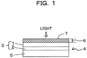
FIG. 1 is a schematic sectional view depicting a configuration of an optical detector according to the present embodiment; -
FIG. 2 is a schematic sectional view depicting an example of a configuration of a region that is provided in the optical detector according to the present embodiment and in which the refractive index varies; -
FIG. 3 is a schematic sectional view depicting another example of a configuration of a region that is provided in the optical detector according to the present embodiment and in which the refractive index varies; -
FIG. 4 is a schematic sectional view depicting a further example of a configuration of a region that is provided in the optical detector according to the present embodiment and in which the refractive index varies; -
FIGS. 5A to 5C are schematic sectional views depicting an example of the configuration of a region that is provided in the optical detector according to the present embodiment and in which the refractive index varies and a comparative example; -
FIGS. 6A and 6B are schematic sectional views illustrating a subject of the present technology; -
FIGS. 7A to 7H are schematic sectional views illustrating an example of a fabrication method of the optical detector according to the present embodiment; -
FIGS. 8A to 8I are schematic sectional views illustrating a different example of the fabrication method of the optical detector according to the present embodiment; and -
FIG. 9 is a schematic view depicting an example of a configuration of an imaging apparatus according to the present embodiment. - In the following, an optical detector and an imaging apparatus according to an embodiment of the present technology are described with reference to the drawings.
- As depicted in
FIG. 1 , the optical detector according to the present embodiment includes asensor device chip 3 including asubstrate 1 and asensor device 2 that is provided at a front face side of thesubstrate 1 and detects light entering from the back face side of thesubstrate 1. - It is to be noted that the
optical detector 4 is also called back incidence type optical detector. Further, inFIG. 1 ,reference numeral 5 denotes a signal processing device joined to thesensor device chip 3. - The
sensor device chip 3 has, at the back face side of thesubstrate 1, aregion 6 in which the refractive index varies so as to increase from a light incident face (light reception face) 7 toward the thicknesswise direction. Here, theregion 6 in which the refractive index varies is a region in which the refractive index varies gradually. It is to be noted that the back face of thesubstrate 1 is the back face of thesensor device chip 3. - Consequently, reflection of light in the region including the
light incident face 7 at the back face side of thesubstrate 1 can be reduced. Therefore, theregion 6 in which the refractive index varies functions as a reflection reduction region in which reflection is reduced. - Here, for example, as depicted in
FIGS. 2 and3 , theregion 6 in which the refractive index varies may be configured from a stacked film 12 (17) provided on the back face of thesubstrate 1 and formed from a plurality offilms 8 to 11 (13 to 16) having refractive indexes different from each other. - In this case, the stacked film 12 (17) may be provided on the back face of the
substrate 1 by stacking the plurality offilms 8 to 11 (13 to 16) formed from materials having refractive indexes different from each other such that the refractive index decreases gradually. In this case, the refractive index increases gradually from thelight incident face 7 toward the thicknesswise direction. - For example, as depicted in
FIG. 2 , aSi film 8 having a refractive index n = 3.42, aZnS film 9 having a refractive index n = 2.63, an Al2O3film 10 having a refractive index n = 1.77 and a CaF2 film 11 having a refractive index n = 1.43 are stacked in order from thesubstrate 1 side on the back face of theGaSb substrate 1 having a refractive index n = 4 so as to provide thestacked film 12 on the back face of thesubstrate 1. - Reflection of light can be reduced by gradually varying the refractive index such that the refractive index decreases gradually from the refractive index of the substrate 1 (in the example described above, the refractive index n = 4) to the refractive index of the air (refractive index n = 1) in the region including the
light incident face 7 at the back face side of thesubstrate 1 in this manner. - In particular, since variation of the refractive index contributes principally to reflection of light, the reflection of light can be reduced by suppressing sudden variation of the refractive index from the refractive index of the air (refractive index n = 1) to the refractive index of the substrate 1 (in the example described above, the refractive index n = 4) in the region including the
light incident face 7 at the back face side of thesubstrate 1. - Further, for example, as depicted in
FIG. 3 , a plurality ofGaSb films 13 to 16 may be formed by sputtering using masks, which have meshes that indicate gradual increase in roughness thereamong, on the back face of theGaSb substrate 1 such that the plurality ofGaSb films 13 to 16 are stacked in order from thesubstrate 1 side in such a manner that the density gradually decreases, namely, the refractive index gradually decreases, thereby to provide astacked film 17 on the back face of theGaSb substrate 1. In this case, the refractive index (density) gradually increases from thelight incident face 7 toward the thicknesswise direction. Further, the plurality of GaSbfilms 13 to 16 have holes having sizes different from each other. - In this manner, reflection of light can be reduced by setting the density so as to gradually decrease toward the
light incident face 7 in the region including thelight incident face 7 at the back face side of thesubstrate 1 and varying the refractive index moderately such that the refractive index gradually decreases from the refractive index of the substrate 1 (in the example described above, the refractive index n = 4) to the refractive index of the air (refractive index n = 1). - Further, it is preferable for the stacked film 12 (17) to have irregularities at a boundary region between adjacent ones of the plurality of
films 8 to 11 (13 to 16). Consequently, moderate variation of the refractive index in the boundary region (interface) between the plurality offilms 8 to 11 (13 to 16) can be implemented and reflection of light on the interface can be suppressed. - For example, by providing irregularities on the back face of the
substrate 1, the stacked film 12 (17) stacked on the back face of thesubstrate 1 has irregularities in the boundary region between the plurality offilms 8 to 11 (13 to 16). Further, since the irregularities are provided intentionally, it is preferable to set the height (depth) of the irregularities to approximately 10 nm or more (for example, several 10 nm) taking the difficulty of production of the irregularities into consideration. - Incidentally, the
region 6 in which the refractive index varies may be provided as a region at the back face side of thesubstrate 1 and in aporous structure 18 as depicted inFIG. 4 . In this case, theregion 6 in which the refractive index varies is a porous region having a porous property. - In particular, the
region 6 in which the refractive index varies may be configured by configuring the region including thelight incident face 7 at the back face side of thesubstrate 1 in theporous structure 18 such that the density (refractive index) of theporous structure 18 gradually varies from thelight incident face 7 toward the thicknesswise direction (inside). - In this case, the
region 6 in which the refractive index varies is a region in which the density varies and is configured from theporous structure 18 in which the density (refractive index) gradually varies. - The
porous structure 18 in which the density (refractive index) gradually increases from thelight incident face 7 toward the thicknesswise direction (inside) may be provided in the region including thelight incident face 7 at the back face side of thesubstrate 1. In this case, in theporous structure 18, the density (refractive index) gradually decreases from the front face, namely, from the inside, toward thelight incident face 7. - By providing such a
porous structure 18 as described above such that the density gradually decreases from the inside toward thelight incident face 7 in the region including thelight incident face 7 at the back face side of thesubstrate 1 and the refractive index moderately varies such that the refractive index gradually decreases from the refractive index of thesubstrate 1 to the refractive index of the air, reflection of light can be reduced. - For example, by performing ion implantation of Sn (Sn+) into the region at the back face side of the
GaSb substrate 1, such aporous structure 18 as described above can be provided in the region including thelight incident face 7 at the back face side of thesubstrate 1. In particular, by performing ion implantation of Sn (Sn+) into the region at the back face side of theGaSb substrate 1, self-organizing formation of such aporous structure 18 as described above is implemented in the region including thelight incident face 7 at the back face side of thesubstrate 1. - In particular, for example, by performing ion implantation of Sn+ into the region at the back face side of the
GaSb substrate 1 by 60 keV and 8.9 × 10¹⁴ ions/cm2, self-organizing formation of such aporous structure 18 as described above is implemented. - It is to be noted that, for example, also by performing ion implantation of Ga+ into the region at the back face side of the
GaSb substrate 1 by 30 keV and 1 × 10¹⁴ ions/cm2, self-organizing formation of such aporous structure 18 as described above is implemented. - Where such a
porous structure 18 as described above is provided by ion implantation in such a manner as described above, it is preferable to set the ion implantation amount, for example, to approximately 4 × 10¹⁴ ions/cm2 to 1.5 × 10¹⁵ ions/cm2. Consequently, the reflection suppression effect can be enhanced. - It is to be noted that the
substrate 1 is not limited to this, and, for example, a GaSb substrate, an InSb substrate, a Ge substrate, a Si substrate or an InP substrate can be used for thesubstrate 1. Further, an element (implantation ion) upon ion implantation is not limited to this, and an element such as, for example, Ga (Ga+), Sn (Sn+), N (N+, N2 +), Ar, Xe, Kr or Ne can be used. - Where the
porous structure 18 is provided in the region including thelight incident face 7 at the back face side of thesubstrate 1 in such a manner as described above, theregion 6 in which the refractive index varies is a region at the back face side of thesubstrate 1 and has a self-organizing structure by the ion implantation. - Further, the
region 6 in which the refractive index varies is a region at the back face side of thesubstrate 1 and has a composition different from that of the other region of thesubstrate 1. In particular, where theporous structure 18 is provided by ion implantation into the region at the back face side of thesubstrate 1, the ion-implanted element remains in the region in which the ion implantation is performed, namely, in theregion 6 in which the refractive index varies. Therefore, theregion 6 in which the refractive index varies has a composition different from that of the other region of thesubstrate 1. - Further, the
region 6 in which the refractive index varies is a region at the back face side of thesubstrate 1 and is a region in which a greater amount of Ga than that of the different region of thesubstrate 1 is contained or one of elements such as Sn, N, Ar, Xe, Kr and Ne is contained. - Incidentally, as depicted in
FIG. 4 , theporous structure 18 configured in such a manner as described above has fine holes extending in the thicknesswise direction of thesubstrate 1. - In this case, the
region 6 in which the refractive index varies is a region at the back face side of thesubstrate 1 and hasprojections 19 having a column shape, a wall shape, a conical shape or a pyramidal shape. Further, theprojections 19 are disposed at random (random structure) . - It is to be noted that also it can be considered that the fine holes configuring the
porous structure 18 have a column shape, a wall shape or the like. Also it can be considered that the fine holes have a random structure. Further, the height of the projections and the depth of the holes may be same as each other or different from each other. - In this manner, where the
region 6 in which the refractive index varies is the region at the back face side of thesubstrate 1 and has theprojections 19 having a column shape, a wall shape, a conical shape or a pyramidal shape, in order to reduce reflection of light, it is ideal that theprojections 19 have such shapes as depicted, for example, inFIGS. 5A and 5B and the density (refractive index) gradually increases toward the thicknesswise direction (depthwise direction) of thesubstrate 1. - Further, it is preferable to set the distance between the holes configuring the
porous structure 18 or theprojections 19 to one half or less of the wavelength of light to be detected. - For example, where the
sensor device 2 is configured to detect light in an infrared region of a wavelength of approximately 0.7 µm to 15 µm, it is preferable to set the distance between the holes configuring theporous structure 18 or theprojections 19 to one half or less of a wavelength included in the wavelength region. For example, it is preferable to set the distance between (cycle of) the holes configuring theporous structure 18 or theprojections 19 to a distance (cycle) less than approximately 0.5 µm. In other words, it is preferable to set the distance between (cycle of) the holes configuring theporous structure 18 or theprojections 19 to a submicron cycle shorter than the signal wavelength. - It is to be noted that, although the holes configuring the
porous structure 18 or theprojections 15 are not limited particularly in depth or height, if, for example, attenuation and so forth are taken into consideration, then it is preferable to set the depth or the height to less than approximately 1 µm. Further, it is preferable to provide no top face to theprojections 19 and provide no bottom face to the holes, namely, it is preferable to provide no flat portion in a region to which light is incident, and even if a flat portion exists, it is preferable to set the portion to a smaller size than approximately 0.5 µm. - Here, the density (refractive index) gradually varies over the
overall substrate 1 in the thicknesswise direction and the top face of theprojections 19 and the bottom face of the holes are not flat. Thus, since there is no flat location in the region to which the light is incident (refer toFIGS. 4 ,5A and 5B ), a low reflectance can be implemented by a moth-eye effect. For example, it is possible to reduce the reflectance so as to be lower than approximately 5 %, and the sensitivity of the sensor can be enhanced significantly. - In contrast, if the top face of the projections or the bottom face of the holes is flat and there is a flat location in the region to which light is incident (refer to
FIG. 5C ), then it is difficult to sufficiently reduce the reflection. - It is to be noted that, in order to achieve enhancement of the sensitivity of the
optical detector 4, it seems recommendable to reduce the thickness of thesubstrate 1 to suppress absorption in the substrate 1 (for example, refer toFIG. 6A ). However, since, for example, approximately 20 % of light is reflected by thelight incident face 7, the efficiency is low and it is insufficient in order to achieve enhancement of the sensitivity. Further, in order to implement substrate thickness reduction control, it seems recommendable to provide anetching stop layer 20 in thesubstrate 1 and reduce the thickness of thesubstrate 1 by etching (for example, refer toFIG. 6B ). However, since light is reflected also by the interface between theetching stop layer 20 and thesubstrate 1, light that reaches the sensor device is, for example, approximately 64 % and this is insufficient in order to implement enhancement of the sensitivity. - On the other hand, by providing the
region 6 in which the refractive index varies as described above, especially, by providing theporous structure 18 in theregion 6, the reflectance can be reduced so as to be lower than approximately 5 % and light that reaches thesensor device 2 increases, for example, to approximately 95 %. Therefore, in comparison with an alternative case in which theetching stop layer 20 is provided (for example, refer toFIG. 6B ), the sensitivity of the sensor can be improved to approximately 1.5 times and improvement of the sensitivity can be implemented. It is to be noted that, by adopting such a configuration as described above, theetching stop layer 20 may not be provided. - Incidentally, the
optical detector 4 configured in such a manner as described above can be applied, for example, to an infrared detector (infrared sensor) or a solar cell. - For example, where the
optical detector 4 is applied to an infrared detector, thesensor device 2 may be configured as an infrared sensor device (IR sensor) that detects light, for example, in the infrared region of a wavelength of approximately 0.7 µm to approximately 15 µm. In this case, thesensor device 2 is provided, at the front face side of thesubstrate 1, as a device having, for example, a superlattice structure, a quantum well structure, a quantum dot structure or the like. It is to be noted that thesensor device 2 is also called sensor device array. - The
signal processing device 5 having an electronic circuit formed, for example, on the surface of a silicon substrate is joined to thesensor device 2 provided at the front face side of thesubstrate 1 as described through a joining portion such as, for example, bumps 23 (for example, refer toFIGS. 1 ,7H and8I ). It is to be noted that thesignal processing device 5 is also called signal processing package or signal processing circuit chip. - Now, a fabrication method for the
optical detector 4 according to the present embodiment is described with reference toFIGS. 7A to 7H and8A to 8I . - Here, description is given taking a case in which an infrared sensor device (backside illumination type infrared sensor device) 2 is provided on a
GaSb substrate 1 to produce an infraredsensor device chip 3 and asignal processing device 5 is joined to the infraredsensor device chip 3 throughbumps 23 to fabricate aninfrared detector 4 as an example. - First, description is given with reference to
FIGS. 7A to 7H taking a case in which aninfrared sensor device 2 is produced on a face reduced in thickness (thin face) of thesubstrate 1 as an example. - First, as depicted in
FIG. 7A , asupport substrate 21 is attached to the back face side of aGaSb substrate 1, which is the back face of an infraredsensor device chip 3. - For example, a SiO2 film 22 (for example, approximately 100 nm thick) is deposited on the back face of the
GaSb substrate 1, for example, by a PE-CVD (plasma-enhanced chemicalvapor deposition) method, and a silicon substrate (Si-sub) is joined as thesupport substrate 21 to theGaSb substrate 1 at a room (ordinary) temperature through the SiO2 film 22. - Then, the
GaSb substrate 1 is thinned as depicted inFIG. 7B . - For example, the
GaSb substrate 1 on which theinfrared sensor device 2 is to be provided is thinned at the front face side thereof to approximately 10 µm from the front face, for example, by back grind and chemical mechanical polishing (CMP), and then chemical cleaning (etch) is performed. - Then, an infrared sensor device (IR sensor) 2 is formed on the thinned face as depicted in
FIG. 7C . - For example, the
infrared sensor device 2 including a superlattice structure or the like is formed by an MBE (Molecular Beam Epitaxy) method. - Then, as depicted in
FIG. 7D , asignal processing device 5 is joined after dicing the wafer into individual chips. - For example, after dicing the wafer into individual chips, a signal processing device (Si-device or PKG) 5 including an electronic circuit formed on the front face of a silicon substrate is stacked and is joined through In bumps 23, whereafter underfill is injected into gaps between the In bumps 23 (not depicted).
- Then, as depicted in
FIG. 7E , the silicon substrate as thesupport substrate 21 is removed. - For example, the silicon substrate as the
support substrate 21 is removed by grinding while leaving a thickness of, for example, approximately 10 µm and a natural oxidation film is removed, whereafter the silicon substrate is soaked in TMAH (tetramethylammonium hydroxide; for example, approximately 70°C) thereby to remove thesilicon substrate 21. - It is to be noted that the
signal processing device 5 may be protected by forming a SiO2 film (for example, approximately 1 µm) on the overall area (overall face) after the bump joining. - Thereafter, the SiO2 film 22 is removed as depicted in
FIG. 7F . - For example, the
signal processing device 5 is soaked in d-HF (ratio of 1 % of hydrofluoric acid to water) to remove the SiO2 film 22 on the joining face between theGaSb substrate 1 and the silicon substrate as thesupport substrate 21. - Then, ion implantation is performed for a region at the back face side of the
GaSb substrate 1 as depicted inFIG. 7G to form aporous structure 18 in which the density varies from the front face side to the inside. Consequently, the region in which the density varies, namely, theregion 6 in which the refractive index varies, is formed in the region at the back face side of theGaSb substrate 1. Theregion 6 in which the refractive index varies (region in which the density varies) functions as a reflection suppression region. - For example, by performing ion implantation of Ga (Ga+) for the region at the back face side of the
GaSb substrate 1 by 60 keV, 1 × 10¹⁵ ions/cm2 and 150K, theporous structure 18 in which the density (refractive index) gradually increases from thelight incident face 7 toward the thicknesswise direction (toward the inside) is formed in theregion 6 including thelight incident face 7 at the back face side of thesubstrate 1 by self-organizing formation. - Then, since the surface at the back face side of the
GaSb substrate 1 on which such aporous structure 18 as described above is formed is unstable as depicted inFIG. 7H , aprotective film 24 is formed so as to cover the surface at the back face side of theGaSb substrate 1 on which such aporous structure 18 as described above is formed. - For example, a SiO2 film having a thickness of, for example, approximately 10 nm is formed as the
protective film 24 by the ALD (Atomic Layer Deposition) method. - In this manner, the
infrared detector 4 that includes the infraredsensor device chip 3 on which theinfrared sensor device 2 is produced on the face (thinned face) formed by thinning thesubstrate 1 can be fabricated. - It is to be noted here that, although the
porous structure 18 is formed after thesupport substrate 21 is removed, formation of theporous structure 18 is not limited to this and theporous structure 18 may be formed before thesupport substrate 21 is attached. - Now, an example in which a
porous structure 18 as a reflection suppression structure is produced on a face (thinned face) formed by thinning thesubstrate 1 is described with reference toFIGS. 8A to 8I . - First, as depicted in
FIG. 8A , a BG (back grind)tape 25 is attached and temporarily fixed to the front face side (device production face) of aGaSb substrate 1 on which aninfrared sensor device 2 is to be provided. - Then, as depicted in
FIG. 8B , theGaSb substrate 1 is thinned. - For example, the
GaSb substrate 1 is thinned at the back face side thereof that serves as the back face of the infraredsensor device chip 3 from the front face thereof, for example, to approximately 10 µm by back grind and CMP, whereafter liquid cleaning (etch) is performed. - Then, as depicted in
FIG. 8C , asupport substrate 21 is attached to the thinned face. - For example, a silicon substrate (Si-sub; or glass substrate) as the
support substrate 21 is joined (room temperature bonding) to the thinned face at the back face side of theGaSb substrate 1 that serves as the back face of the infraredsensor device chip 3. - Then, as depicted in
FIG. 8D , theBG tape 25 is removed. - Then, as depicted in
FIG. 8E , an infrared sensor device (IR sensor) 2 is formed at the front face side of theGaSb substrate 1. - For example, the
infrared sensor device 2 including a superlattice structure or the like is formed by the MBE method. - Then, as depicted in
FIG. 8F , asignal processing device 5 is joined after dicing the wafer into individual chips. - For example, after dicing the wafer into individual chips, a signal processing device (Si-device or PKG) 5 including an electronic circuit formed on the front face of a silicon substrate is stacked and then is joined through In bumps 23, whereafter underfill is injected into gaps between the In bumps 23 (not depicted).
- Thereafter, as depicted in
FIG. 8G , the silicon substrate (or the glass substrate) as thesupport substrate 21 is removed. For example, thesupport substrate 21 may be removed by back grind and etching using chemical liquid. - Then, as depicted in
FIG. 8H , ion implantation for the region at the back face side of theGaSb substrate 1 is performed to form aporous structure 18 in which the density varies from the front face side to the inside. Consequently, a region in which the density varies, namely, theregion 6 in which the refractive index varies, is formed in the region at the back face side of thesubstrate 1. Theregion 6 in which the refractive index varies (region in which the density varies) functions as the reflection suppression region. - For example, by performing ion implantation of Ga (Ga+) for the region at the back face side of the
GaSb substrate 1 by 60 keV, 1 × 10¹⁵ ions/cm2 and 150K, theporous structure 18 in which the density (refractive index) gradually increases from thelight incident face 7 toward the thicknesswise direction (toward the inside) is formed in the region including thelight incident face 7 at the back face side of theGaSb substrate 1 by self-organizing formation. - Then, since the surface at the back face side of the
GaSb substrate 1 on which such aporous structure 18 as described above is formed is unstable as depicted inFIG. 8I , aprotective film 24 is formed so as to cover the surface at the back face side of theGaSb substrate 1 on which such aporous structure 18 as described above is formed. - For example, a SiO2 film having a thickness of, for example, approximately 10 nm is formed as the
protective film 24 by the ALD method. - The
infrared detector 4 including the infraredsensor device chip 3 on which theporous structure 18 as a reflection suppression structure is produced on the face (thinned face) formed by thinning thesubstrate 1 can be fabricated. - It is to be noted here that, while the
porous structure 18 is formed after thesupport substrate 21 is removed, the formation of theporous structure 18 is not limited to this and theporous structure 18 may be formed after theGaSb substrate 1 is thinned before thesupport substrate 21 is attached. - It is to be noted that the formation method of the
porous structure 18 is not limited to that described above. - For example, the
region 6 in which the refractive index varies may be provided in the region at the back face side of thesubstrate 1 by controlling the density variation, for example, by wet etching or dry etching after the region at the back face side of the substrate is configured as a porous region by anodization. In this case, theregion 6 in which the refractive index varies may be provided, for example, by adjusting the etching time to control the diameter or the depth of the porous region so as to gradually vary the density (refractive index) of the porous region from the light incident face toward the thicknesswise direction. - Further, the
region 6 in which the refractive index varies may be provided by forming a thin film (for example, of silicon or the like) at the back face side of the substrate first, converting the thin film into a porous film by anodization and then performing dry etching such as, for example, RIE using the porous film as a mask to form a porous region, in which the density variation is controlled, in the region at the back face side of thesubstrate 1. In this case, theregion 6 in which the refractive index varies may be provided, for example, by adjusting the etching time or the like to control the diameter or the depth of the porous region so as to gradually vary the density (refractive index) of the porous region from the light incident face toward the thicknesswise direction. - It is to be noted here that, while the porous film is used as a mask, the method is not limited to this, and the
region 6 in which the refractive index varies may be provided by performing dry etching or wet etching using a mask to form a porous region, in which the density variation is controlled, in the region at the back face side of thesubstrate 1. - Incidentally, an imaging apparatus can be configured as an apparatus that includes the
optical detector 4 configured in such a manner as described above. - For example, where the
optical detector 4 configured in such a manner as described above is applied to an infrared detector and an imaging apparatus is configured as an apparatus including the infrared detector, the imaging apparatus (infrared imaging apparatus) may be configured in the following manner. - For example, as depicted in
FIG. 9 , an imaging apparatus (infrared imaging apparatus) 30 may include an optical detector (infrared detector) 4 configured as a device that includes the infraredsensor device chip 3 and thesignal processing device 5 as described above, a controlarithmetic unit 31 that performs signal processing and various kinds of control, and amonitor 32 that displays an image obtained by imaging. - Then, the
infrared detector 4 configured in such a manner as described above may be provided in a vacuum container (detector container) 34 into which infrared rays enter through alens 33 such that theinfrared detector 4 is attached to and cooled by acold head 36 coupled to a cooling system (refrigerator) 35. - Further, the control
arithmetic unit 31 may be coupled to thesignal processing device 5 provided in theinfrared detector 4 configured as described above such that an output signal from thesignal processing device 5 is sent to and processed by the controlarithmetic unit 31. - Further, the control
arithmetic unit 31 may be configured from a computer or a controller. Further, the controlarithmetic unit 31 may include a drive circuit or a signal processing circuit such that it outputs power, a driving pulse or the like for driving the infraredsensor device chip 3 included in theinfrared detector 4 configured in such a manner as described above and performs a process for an output signal from the infraredsensor device chip 3 and then outputs an image signal to themonitor 32. - It is to be noted that the configuration of the imaging apparatus is not limited to this, and the imaging apparatus may include the
infrared detector 4 configured in such a manner as described above and a control arithmetic unit coupled to theinfrared detector 4.
Claims (12)
- An optical detector, comprising:a sensor device chip (3) including a substrate (1) and a sensor device (2) that is provided at a front face side of the substrate and detects light entering from a back face side of the substrate;wherein the sensor device chip has, at the back face side of the substrate, a region (6) in which a refractive index varies so as to increase from a light incident face (7) toward a thicknesswise direction.
- The optical detector according to claim 1, wherein the region (6) in which the refractive index varies is configured from a stacked film (12, 17) that is provided on the back face of the substrate (1) and in which a plurality of films (8-11, 13-16) having refractive indexes different from each other are stacked.
- The optical detector according to claim 2, wherein the stacked film (12, 17) has irregularities at a boundary portion between the plurality of films.
- The optical detector according to claim 1, wherein the region (6) in which the refractive index varies- is a region at the back face side of the substrate (1) and has a porous structure (18).
- The optical detector according to claim 1, wherein the region (6) in which the refractive index varies is a region at the back face side of the substrate (1) and has projections (19) having a pillar shape, a wall shape, a conical shape or a pyramidal shape.
- The optical detector according to claim 5, wherein the projections (19) are disposed at random.
- The optical detector according to any one of claims 4 to 6, wherein a distance between porosities configuring the porous structure (18) or between the projections (19) is equal to or smaller than one half a wavelength of light to be detected.
- The optical detector according to claim 1, wherein the substrate (1) is a GaSb substrate, an InSb substrate, a Ge substrate, a Si substrate or an InP substrate; and
the region (6) in which the refractive index varies is a region at the back face side of the substrate and has a self-organizing structure by ion implantation. - The optical detector according to claim 1, wherein the substrate (1) is a GaSb substrate, an InSb substrate, a Ge substrate, a Si substrate or an InP substrate; and
the region (6) in which the refractive index varies is a region at the back face side of the substrate and has a composition different from that of a different region of the substrate. - The optical detector according to claim 1, wherein the substrate (1) is a GaSb substrate, an InSb substrate, a Ge substrate, a Si substrate or an InP substrate; and
the region (6) in which the refractive index varies is a region at the back face side of the substrate and contains Ga by a greater amount than the other region of the substrate or contains one of elements of Sn, N, Ar, Xe, Kr and Ne. - The optical detector according to any one of claims 1 to 10, wherein the sensor device (2) detects light of an infrared region of a wavelength from 0.7 µm to 15 µm.
- An imaging apparatus, comprising:an optical detector (4); anda control arithmetic unit (31) coupled to the optical detector;wherein the optical detection (4) includesa sensor device chip (3) including a substrate (1) and a sensor device (2) that is provided at a front face side of the substrate and detects light entering from a back face side of the substrate; andwherein the sensor device chip has, at the back face side of the substrate, a region (6) in which a refractive index varies so as to increase from a light incident face (7) toward a thicknesswise direction.
Applications Claiming Priority (1)
| Application Number | Priority Date | Filing Date | Title |
|---|---|---|---|
| JP2016253197A JP2018107314A (en) | 2016-12-27 | 2016-12-27 | Photodetector and imaging device |
Publications (1)
| Publication Number | Publication Date |
|---|---|
| EP3343250A1 true EP3343250A1 (en) | 2018-07-04 |
Family
ID=60515168
Family Applications (1)
| Application Number | Title | Priority Date | Filing Date |
|---|---|---|---|
| EP17204194.9A Withdrawn EP3343250A1 (en) | 2016-12-27 | 2017-11-28 | Optical detector and imaging apparatus |
Country Status (3)
| Country | Link |
|---|---|
| US (1) | US10079258B2 (en) |
| EP (1) | EP3343250A1 (en) |
| JP (1) | JP2018107314A (en) |
Families Citing this family (1)
| Publication number | Priority date | Publication date | Assignee | Title |
|---|---|---|---|---|
| US12613197B2 (en) | 2019-12-03 | 2026-04-28 | Kla Corporation | Low-reflectivity back-illuminated image sensor |
Family Cites Families (9)
| Publication number | Priority date | Publication date | Assignee | Title |
|---|---|---|---|---|
| JP2860028B2 (en) | 1992-11-26 | 1999-02-24 | 株式会社フジクラ | Ultraviolet detector and method of manufacturing the same |
| US6790502B1 (en) * | 1999-10-15 | 2004-09-14 | Hitachi, Ltd. | Optically functional element and production method and application therefor |
| JP2008066584A (en) | 2006-09-08 | 2008-03-21 | Asahi Kasei Electronics Co Ltd | Optical sensor |
| TWI455326B (en) * | 2007-09-13 | 2014-10-01 | Omnivision Tech Inc | Transmissive detector, system using the same and method thereof |
| KR20120012555A (en) * | 2010-08-02 | 2012-02-10 | 광주과학기술원 | Gradually varying refractive index of the silicon multilayer anti-reflective film, a method of manufacturing the same and a solar cell having the same and a method of manufacturing the same |
| US9231061B2 (en) * | 2010-10-25 | 2016-01-05 | The Research Foundation Of State University Of New York | Fabrication of surface textures by ion implantation for antireflection of silicon crystals |
| JP5829223B2 (en) | 2013-01-17 | 2015-12-09 | 浜松ホトニクス株式会社 | Photodiode manufacturing method and photodiode |
| JP2015220313A (en) * | 2014-05-16 | 2015-12-07 | ソニー株式会社 | Solid-state image pickup device and its manufacturing method, and electronic apparatus |
| JP7023109B2 (en) * | 2015-06-05 | 2022-02-21 | ソニーグループ株式会社 | Solid-state image sensor |
-
2016
- 2016-12-27 JP JP2016253197A patent/JP2018107314A/en active Pending
-
2017
- 2017-11-28 EP EP17204194.9A patent/EP3343250A1/en not_active Withdrawn
- 2017-11-29 US US15/825,704 patent/US10079258B2/en not_active Expired - Fee Related
Non-Patent Citations (4)
| Title |
|---|
| A.K.SOOD ET AL.: "DESIGN AND DEVELOPMENT OF HIGH PERFORMANCE RADIATION HARDENED ANTI-REFLECTION COATINGS FOR LWIR HGCDTE FOCAL PLANE ARRAYS", INFRARED DETECTOR MATERIALS AND DEVICES, SPIE PROCCEEDINGS, vol. 5564, 2004, pages 15 - 26, XP040191379 * |
| HOBBS D S ET AL: "Design, fabrication, and measured performance of anti-reflecting surface textures in infrared transmitting materials", VISUAL COMMUNICATIONS AND IMAGE PROCESSING; 20-1-2004 - 20-1-2004; SAN JOSE,, vol. 5786, no. 1, 28 March 2005 (2005-03-28), pages 349 - 364, XP002442432, ISBN: 978-1-62841-730-2, DOI: 10.1117/12.604532 * |
| KADAKIA NIRAG ET AL: "Fabrication of surface textures by ion implantation for antireflection of silicon crystals", APPLIED PHYSICS LETTERS, A I P PUBLISHING LLC, US, vol. 97, no. 19, 12 November 2010 (2010-11-12), pages 191912 - 191912, XP012137593, ISSN: 0003-6951, DOI: 10.1063/1.3515842 * |
| MARTIN F. SCHUBERT ET AL: "Design of multilayer antireflection coatings made from co-sputtered and low-refractive-index materials by genetic algorithm", OPTICS EXPRESS, vol. 16, no. 8, 14 April 2008 (2008-04-14), pages 5290 - 176, XP055474378, DOI: 10.1364/OE.16.005290 * |
Also Published As
| Publication number | Publication date |
|---|---|
| US20180182799A1 (en) | 2018-06-28 |
| JP2018107314A (en) | 2018-07-05 |
| US10079258B2 (en) | 2018-09-18 |
Similar Documents
| Publication | Publication Date | Title |
|---|---|---|
| US11721714B2 (en) | Pixel isolation elements, devices and associated methods | |
| US8664578B2 (en) | Image sensor with reduced crosstalk having an isolation region with a second trench in the electrically conductive material of a first trench | |
| US11189657B2 (en) | Image sensor with improved quantum efficiency surface structure | |
| US8674283B2 (en) | Image sensor with reduced optical crosstalk | |
| CN106531750B (en) | The CMOS image sensor structure improved with crosstalk | |
| TWI760010B (en) | Image sensor, optical structure and methods of forming the same | |
| US20180216928A1 (en) | Three dimensional imaging utilizing stacked imager devices and associated methods | |
| CN106057837B (en) | CMOS Image Sensor Structure | |
| JP2010056167A (en) | Solid-state image pickup element and manufacturing method thereof | |
| US20200266232A1 (en) | Image sensor with improved quantum efficiency surface structure | |
| TW201436183A (en) | Image sensor device and method of manufacturing same | |
| CN105070732B (en) | High pixel image sensor package and preparation method thereof | |
| CN104952895A (en) | Semiconductor wafer, method for manufacturing light receiving sensor, and light receiving sensor | |
| US10079258B2 (en) | Optical detector and imaging apparatus | |
| CN107134468A (en) | 3-dimensional image sensor and its manufacture method | |
| WO2013056249A1 (en) | Three dimensional architecture semiconductor devices and associated methods | |
| US12148755B2 (en) | Front-side-type image sensor | |
| CN109950267B (en) | Method for manufacturing image sensor | |
| US20240355851A1 (en) | Photoelectric sensor and fabrication method thereof, and electronic device | |
| CN117153853A (en) | Photoelectric sensor, forming method thereof and electronic equipment | |
| WO2018061898A1 (en) | Optical sensor and method for forming same | |
| TW202226562A (en) | Short-wave infrared focal plane arrays, and methods for utilization and manufacturing thereof | |
| EP2974302B1 (en) | Three dimensional imaging utilizing stacked imager devices and associated methods | |
| CN110459552A (en) | Method of forming image sensor |
Legal Events
| Date | Code | Title | Description |
|---|---|---|---|
| PUAI | Public reference made under article 153(3) epc to a published international application that has entered the european phase |
Free format text: ORIGINAL CODE: 0009012 |
|
| STAA | Information on the status of an ep patent application or granted ep patent |
Free format text: STATUS: THE APPLICATION HAS BEEN PUBLISHED |
|
| AK | Designated contracting states |
Kind code of ref document: A1 Designated state(s): AL AT BE BG CH CY CZ DE DK EE ES FI FR GB GR HR HU IE IS IT LI LT LU LV MC MK MT NL NO PL PT RO RS SE SI SK SM TR |
|
| AX | Request for extension of the european patent |
Extension state: BA ME |
|
| STAA | Information on the status of an ep patent application or granted ep patent |
Free format text: STATUS: REQUEST FOR EXAMINATION WAS MADE |
|
| 17P | Request for examination filed |
Effective date: 20181024 |
|
| RBV | Designated contracting states (corrected) |
Designated state(s): AL AT BE BG CH CY CZ DE DK EE ES FI FR GB GR HR HU IE IS IT LI LT LU LV MC MK MT NL NO PL PT RO RS SE SI SK SM TR |
|
| STAA | Information on the status of an ep patent application or granted ep patent |
Free format text: STATUS: EXAMINATION IS IN PROGRESS |
|
| 17Q | First examination report despatched |
Effective date: 20191125 |
|
| STAA | Information on the status of an ep patent application or granted ep patent |
Free format text: STATUS: THE APPLICATION IS DEEMED TO BE WITHDRAWN |
|
| 18D | Application deemed to be withdrawn |
Effective date: 20220601 |