EP3340749A1 - Cooling conductive trace with pressurized air or gas - Google Patents
Cooling conductive trace with pressurized air or gas Download PDFInfo
- Publication number
- EP3340749A1 EP3340749A1 EP17208637.3A EP17208637A EP3340749A1 EP 3340749 A1 EP3340749 A1 EP 3340749A1 EP 17208637 A EP17208637 A EP 17208637A EP 3340749 A1 EP3340749 A1 EP 3340749A1
- Authority
- EP
- European Patent Office
- Prior art keywords
- metallic
- conductive trace
- electrical assembly
- assembly according
- channels
- Prior art date
- Legal status (The legal status is an assumption and is not a legal conclusion. Google has not performed a legal analysis and makes no representation as to the accuracy of the status listed.)
- Granted
Links
Images



Classifications
-
- H—ELECTRICITY
- H05—ELECTRIC TECHNIQUES NOT OTHERWISE PROVIDED FOR
- H05K—PRINTED CIRCUITS; CASINGS OR CONSTRUCTIONAL DETAILS OF ELECTRIC APPARATUS; MANUFACTURE OF ASSEMBLAGES OF ELECTRICAL COMPONENTS
- H05K1/00—Printed circuits
- H05K1/02—Details
- H05K1/0201—Thermal arrangements, e.g. for cooling, heating or preventing overheating
- H05K1/0203—Cooling of mounted components
-
- H—ELECTRICITY
- H05—ELECTRIC TECHNIQUES NOT OTHERWISE PROVIDED FOR
- H05K—PRINTED CIRCUITS; CASINGS OR CONSTRUCTIONAL DETAILS OF ELECTRIC APPARATUS; MANUFACTURE OF ASSEMBLAGES OF ELECTRICAL COMPONENTS
- H05K1/00—Printed circuits
- H05K1/02—Details
- H05K1/0201—Thermal arrangements, e.g. for cooling, heating or preventing overheating
-
- H—ELECTRICITY
- H05—ELECTRIC TECHNIQUES NOT OTHERWISE PROVIDED FOR
- H05K—PRINTED CIRCUITS; CASINGS OR CONSTRUCTIONAL DETAILS OF ELECTRIC APPARATUS; MANUFACTURE OF ASSEMBLAGES OF ELECTRICAL COMPONENTS
- H05K1/00—Printed circuits
- H05K1/02—Details
- H05K1/0272—Adaptations for fluid transport, e.g. channels, holes
-
- H—ELECTRICITY
- H05—ELECTRIC TECHNIQUES NOT OTHERWISE PROVIDED FOR
- H05K—PRINTED CIRCUITS; CASINGS OR CONSTRUCTIONAL DETAILS OF ELECTRIC APPARATUS; MANUFACTURE OF ASSEMBLAGES OF ELECTRICAL COMPONENTS
- H05K1/00—Printed circuits
- H05K1/02—Details
- H05K1/0201—Thermal arrangements, e.g. for cooling, heating or preventing overheating
- H05K1/0203—Cooling of mounted components
- H05K1/0209—External configuration of printed circuit board adapted for heat dissipation, e.g. lay-out of conductors, coatings
-
- H—ELECTRICITY
- H05—ELECTRIC TECHNIQUES NOT OTHERWISE PROVIDED FOR
- H05K—PRINTED CIRCUITS; CASINGS OR CONSTRUCTIONAL DETAILS OF ELECTRIC APPARATUS; MANUFACTURE OF ASSEMBLAGES OF ELECTRICAL COMPONENTS
- H05K1/00—Printed circuits
- H05K1/02—Details
- H05K1/0201—Thermal arrangements, e.g. for cooling, heating or preventing overheating
- H05K1/0203—Cooling of mounted components
- H05K1/021—Components thermally connected to metal substrates or heat-sinks by insert mounting
-
- H—ELECTRICITY
- H05—ELECTRIC TECHNIQUES NOT OTHERWISE PROVIDED FOR
- H05K—PRINTED CIRCUITS; CASINGS OR CONSTRUCTIONAL DETAILS OF ELECTRIC APPARATUS; MANUFACTURE OF ASSEMBLAGES OF ELECTRICAL COMPONENTS
- H05K1/00—Printed circuits
- H05K1/02—Details
- H05K1/0296—Conductive pattern lay-out details not covered by sub groups H05K1/02 - H05K1/0295
-
- H—ELECTRICITY
- H05—ELECTRIC TECHNIQUES NOT OTHERWISE PROVIDED FOR
- H05K—PRINTED CIRCUITS; CASINGS OR CONSTRUCTIONAL DETAILS OF ELECTRIC APPARATUS; MANUFACTURE OF ASSEMBLAGES OF ELECTRICAL COMPONENTS
- H05K7/00—Constructional details common to different types of electric apparatus
- H05K7/20—Modifications to facilitate cooling, ventilating, or heating
- H05K7/20009—Modifications to facilitate cooling, ventilating, or heating using a gaseous coolant in electronic enclosures
- H05K7/20136—Forced ventilation, e.g. by fans
- H05K7/20145—Means for directing air flow, e.g. ducts, deflectors, plenum or guides
-
- H—ELECTRICITY
- H05—ELECTRIC TECHNIQUES NOT OTHERWISE PROVIDED FOR
- H05K—PRINTED CIRCUITS; CASINGS OR CONSTRUCTIONAL DETAILS OF ELECTRIC APPARATUS; MANUFACTURE OF ASSEMBLAGES OF ELECTRICAL COMPONENTS
- H05K2201/00—Indexing scheme relating to printed circuits covered by H05K1/00
- H05K2201/06—Thermal details
-
- H—ELECTRICITY
- H05—ELECTRIC TECHNIQUES NOT OTHERWISE PROVIDED FOR
- H05K—PRINTED CIRCUITS; CASINGS OR CONSTRUCTIONAL DETAILS OF ELECTRIC APPARATUS; MANUFACTURE OF ASSEMBLAGES OF ELECTRICAL COMPONENTS
- H05K2201/00—Indexing scheme relating to printed circuits covered by H05K1/00
- H05K2201/06—Thermal details
- H05K2201/064—Fluid cooling, e.g. by integral pipes
-
- H—ELECTRICITY
- H05—ELECTRIC TECHNIQUES NOT OTHERWISE PROVIDED FOR
- H05K—PRINTED CIRCUITS; CASINGS OR CONSTRUCTIONAL DETAILS OF ELECTRIC APPARATUS; MANUFACTURE OF ASSEMBLAGES OF ELECTRICAL COMPONENTS
- H05K2201/00—Indexing scheme relating to printed circuits covered by H05K1/00
- H05K2201/09—Shape and layout
- H05K2201/09009—Substrate related
- H05K2201/09036—Recesses or grooves in insulating substrate
Definitions
- This disclosure relates to cooling a conductive trace with pressurized air or gas and, more particularly, a cooling conductive trace associated with a circuit board or substrate.
- heavy-pour copper traces are used on circuit boards to keep trace resistances low and prevent overheating for high current applications, like power electronics for vehicles.
- the copper traces consume valuable metal resources and add extra weight to the power electronics.
- the size of heavy-pour copper traces may be based on engineering guidelines to allow for maximum allowed current density. High frequency current tends to flow at the surface or skin of the conductor or copper trace, which can increase resistance and contribute to additional thermal loading.
- external cooling may involve placing dielectric thermal interface materials in contact with the copper traces to transfer heat to a heat sink.
- External cooling of copper traces tends to increase the complexity, size, and cost of circuit boards in power electronic systems. Thus, there is need to cool traces without adding thermal interface materials and heat sink.
- an electrical assembly comprises a dielectric substrate and a metallic conductive trace overlying the substrate.
- the metallic conductive trace has a hollow cross-section that forms a duct.
- An annular member protrudes from the metallic conductive trace.
- the annular member has an opening in communication with the duct, the opening for receiving pressurized air or gas.
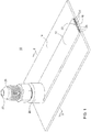
- FIG. 1 is a perspective view of one embodiment of a conductive trace 12 overlying a dielectric substrate 14.
- an electrical assembly 10 comprises a dielectric substrate 14 and a metallic conductive trace 12 overlying the substrate 14 or a dielectric layer of a substrate (e.g., circuit board).
- the metallic conductive trace 12 has a cross-section 18 (e.g., hollow cross section in FIG. 2 ) that forms a duct 22 (e.g., air duct) or conduit suitable for conveying air, gas or a fluid (e.g., fluid in gas phase of matter).
- An annular member 20 protrudes from the metallic conductive trace 12, the dielectric substrate 14, or both.
- the annular member 20 has an opening 24 in communication with the duct 22.
- the opening 24 is arranged to receive compressed or pressurized air or gas (e.g., that is pressurized or compressed to a pressure greater than the ambient atmospheric pressure).
- the opening 24 of the annular member 20 has internal threads 40 for receiving an air hose or a coupler 26 (e.g., threaded coupler) for compressed air or compressed gas (e.g., nitrogen or carbon dioxide) from a compressor or tank of compressed air or gas.
- the coupler 26 e.g., coupler
- the coupler 26 is connected to the annular member 20 and is adapted to receive compressed air or gas at an inlet port 23 from a hose, tube or pneumatic line that is connected to a compressor, a tank or other source of compressed air, gas or fluid.
- a refrigeration system can be used with a compressor that provides compressed refrigerant (e.g., fluid) to the opening 24 or inlet 23 for circulation through the duct 22 or channels 28 (e.g., that function as a condenser) to an outlet of the channels 28 that is connected to an evaporator (e.g., evaporator coil) that returns the cooled refrigerant to the compressor, where refrigerant lines interconnect the compressor, the opening 24, the outlet, and the evaporator as a closed system for recycling the refrigerant.
- compressed refrigerant e.g., fluid
- channels 28 e.g., that function as a condenser
- evaporator e.g., evaporator coil
- the annular member 20 can be composed of a metal, a metal alloy, a plastic, a polymer, a metallic material, or a metallic outer coating or metallic sheath.
- the metallic member may have a cylindrical interior surface 21.
- the coupler 26 is composed of a plastic, a polymer or a dielectric material to provide electrical isolation between the circuit trace 12 and the compressor or tank that provides air or gas to the opening 24.
- the opening 24 of the annular member 20 comprises a generally cylindrical hole that terminates at a surface of the dielectric substrate 14 (e.g., in an elliptical or circular region of the surface of the dielectric substrate 14).
- the duct 22 comprises a plurality of channels 28 that meet the opening 24 at a curved interior surface or the cylindrical interior surface 21 of the opening 24.
- FIG. 2 is a cross-sectional view of the conductive trace 12 along reference line 2-2 of FIG. 1 .
- the hollow cross-section 18 comprises a metallic base wall 34 on the dielectric substrate 14, a plurality of side walls 38 extending vertically from the metallic base wall 34, and a cap wall 36 capping or intersecting the side walls 38.
- the duct 22 comprises a plurality of channels 28 that extend 16 longitudinally through the metallic conductive trace 12, where the channels 28 are generally parallel to each other.
- the channels 28 are capable of communicating the pressurized air or gas between the opening 24 and an opposite end 16 of the channels 28.
- the channels 28 have a substantially rectangular cross section or a substantially polygonal cross section.
- the channels 28 have a substantially circular cross section or a substantially elliptical cross section.
- the substrate 14 comprises a circuit board where the circuit board has a multiple conductive traces 12 in accordance with this disclosure. Each conductive trace 12 may be fed by a separate opening 24 or inlet 23, for instance.
- the end 16 or air output of one conductive trace 12 may be placed in series with another conductive trace 12 by a pneumatically connection between the end and the opening 24.
- the conductive traces 12 with the interior coolant channels 28 can be made or formed by an additive manufacturing process, a subtractive manufacturing process, a combination of an additive manufacturing process and a subtractive manufacturing process, or by a three-dimensional printing process, for example.
- An additive manufacturing process forms the conductive traces 12 with the channels 28 in multiple layers that are stacked or adjoin each other in a successive or iterative process.
- an additive manufacturing process may include three-dimensional printing by a three-dimensional printer from a computer-aided-design (CAD) model or file that defines the conductive trace 12 and cooling channels 28.
- Successive layers of the electrical assembly (10, 110) can be printed and joined by bonding agents or adhesives, for instance.
- Other additive manufacturing processes can be used, such as photolithographic manufacturing processes.
- Photolithographic manufacturing processes can be used to cure a photosensitive polymer layer for addition to a substrate or circuit board by exposure to selective electromagnetic radiation (e.g., ultraviolet light in accordance with a target pattern or mask), whereas other portions that are not irradiated can be removed by subtractive manufacturing process, such as chemical etching, chemical treatment or ablation.
- Metal layers can be produced by metal sputtering, electroplating, or electroless deposition, for example.
- the duct 22 or coolant channels 28 convey forced cool air, nitrogen, carbon dioxide, or gas through the duct 22 from the opening 24 to an outlet at an opposite end 16, which may be discharged to ambient air pressure or collected in a tank for recycling, cooling and compression for reintroduction to the opening 24 or inlet.
- the flow of air, nitrogen or other gas through the duct 22 or channels 28 provides cooling directly to the conductive trace 12 or the high thermal flux areas of the circuit board without the weight or volume of heat sink, or other heat dissipating structures.
- FIG. 3 is a perspective view of another embodiment of a conductive trace 112 overlying a substrate.
- the conductive trace 112 of FIG. 3 is similar to the conductive trace 12 of FIG. 1 and FIG. 2 , except the conductive trace 112 of FIG. 3 has a dielectric core 32 with metallic outer surfaces and metallic channels 28.
- Like reference numbers in FIG. 1 through FIG. 3 , inclusive, indicate like elements.
- the conductive trace 112 has metallic outer surfaces 113, such as an upper exterior surface 300 and side exterior surfaces (302, 304) of a metal or metallic material.
- the dielectric core 32 is bounded by a dielectric substrate 14 or dielectric layer of the circuit board and the metallic outer surfaces 113.
- the duct 122 comprises a plurality of hollow metallic channels 128 that extend 16 longitudinally (along or parallel to a longitudinal axis 306) through an interior region or dielectric core 32 of the metallic conductive trace 112, where the channels 128 are generally parallel to each other.
- Each metallic channel 128 has one or more metallic walls 308.
- the channels 28 are capable of communicating the pressurized air or gas between the opening 24 and an opposite end 116 of the channels 128.
- the metallic channels 128 have a substantially rectangular cross section or a substantially polygonal cross section. In an alternate embodiment, the metallic channels 128 have substantially circular cross section or a substantially elliptical cross section. For example, the metallic channels 128 may be generally tubular.
- the embodiment of FIG. 3 through FIG. 7 may use less metal or alloy than the embodiment of FIG. 1 and FIG. 2 , collectively.
- the embodiment of FIG. 3 through FIG. 7 may be used for transmission of higher frequency signals than the lower frequencies carried by FIG. 1 and FIG. 2 , collectively, where higher frequency signals can be conducted by the outer metallic layer of the conductive trace 112 rather than by the interior electrically conductive portion below the surface of the conductive trace 112.
- FIG. 4 is cross-sectional view of the conductive trace 112 along reference line 4-4 of FIG. 3 .
- the hollow metallic channels 128 are separated by intervening dielectric partitions or a dielectric core 32.
- each hollow metallic channel 128 has a set of walls 308, such as a bottom wall and side walls extending upward from the bottom wall, although other configurations are possible and fall within the scope of the claims of this disclosure.
- the walls 308 are shown in cross section.
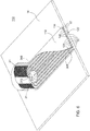
- FIG. 5 is perspective view of the conductive trace 112 of FIG. 3 with a portion cut away to reveal the cross-section 118.
- FIG. 5 illustrates opening 24 in annular member 20 for receiving pressurized air or gas, where the opening 24 communicates with the channels 128.
- the annular member 20 has a group of apertures 310 that radially separated from each other in a substantially cylindrical interior surface 21, where each aperture 310 is connected to (or open to the interior of) a respective channel 128.
- a bottom of the annular member 20 exposes a generally circular region 312 of the dielectric substrate 14 or layer.
- the duct 122 comprises a plurality of channels 128 that meet the opening 24 at a curved interior surface 30 of the opening 24.
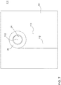
- FIG. 6 is a plan view of the conductive trace 112 of FIG. 3 .
- the opening 24 of the annular member 20 comprises a generally cylindrical hole that terminates at a surface of the dielectric substrate 14 (e.g., in the generally elliptical or circular region 312).
- FIG. 7 is an exploded view of the conductive trace 112 of FIG. 3 where a connector or coupler 26 is removed.
- the opening 24 of the annular member 20 has internal threads 40 for receiving a coupler 26 for compressed air.
- FIG. 7 illustrates internal threads 40 in the annular member 20
- the annular member 20 may have external threads for connection to a source of compressed air or gas.
- the coupler 26 is composed of a plastic, a polymer or a dielectric material.
- the coupler 26 or connector may comprise a metal or metallic member.
- the electrical assembly (110, 10) with the conductive trace (12, 112)of the disclosure is well-suited for dissipating thermal energy from circuit boards, such as circuit boards that use power electronics or that carry high currents.
- An air compressor can compress air, nitrogen or another gas that is forced through the channels (28, 128) to provide cooling or heat dissipation of the circuit trace (12, 112) and any associated heat-generating electrical components, like semiconductor switches, integrated circuits, or power transistors. Forced-air or forced-gas cooling is desirable because unlike liquid cooling media that can be electrically conductive, air (e.g., dry air without salt ions and marine particulate contaminants) is electrically nonconductive.
- the electrical assembly (10, 110) of this disclosure eliminates or reduces the need for thick conductive traces for cooling, such as heavy copper pour traces, or a separate dedicated heatsink and the challenges to prevent coolant leakage and to provide electrical isolation that come with the liquid cooled systems.
- the circuit trace with internal air-cooled channels (28, 128) can facilitate a cost-effective and space efficient circuit board, electrical assembly (10, 110) or electronic assembly, where one or more air-cooled conductive traces (12, 112) are capable of carrying electrical current to one or more electrical or electronic devices, such as power switching transistors, power semiconductors, or integrated circuits.
Landscapes
- Engineering & Computer Science (AREA)
- Microelectronics & Electronic Packaging (AREA)
- Physics & Mathematics (AREA)
- Thermal Sciences (AREA)
- Cooling Or The Like Of Electrical Apparatus (AREA)
- Shielding Devices Or Components To Electric Or Magnetic Fields (AREA)
- Insulators (AREA)
- Waveguide Aerials (AREA)
- Laser Surgery Devices (AREA)
Abstract
Description
- This disclosure relates to cooling a conductive trace with pressurized air or gas and, more particularly, a cooling conductive trace associated with a circuit board or substrate.
- In the certain prior art, heavy-pour copper traces are used on circuit boards to keep trace resistances low and prevent overheating for high current applications, like power electronics for vehicles. The copper traces consume valuable metal resources and add extra weight to the power electronics. The size of heavy-pour copper traces may be based on engineering guidelines to allow for maximum allowed current density. High frequency current tends to flow at the surface or skin of the conductor or copper trace, which can increase resistance and contribute to additional thermal loading.
- In some prior art, to keep temperature of the copper traces and circuit board under allowed maximum, external cooling is used. For example, external cooling may involve placing dielectric thermal interface materials in contact with the copper traces to transfer heat to a heat sink. External cooling of copper traces tends to increase the complexity, size, and cost of circuit boards in power electronic systems. Thus, there is need to cool traces without adding thermal interface materials and heat sink.
- In accordance with on embodiment, an electrical assembly comprises a dielectric substrate and a metallic conductive trace overlying the substrate. The metallic conductive trace has a hollow cross-section that forms a duct. An annular member protrudes from the metallic conductive trace. The annular member has an opening in communication with the duct, the opening for receiving pressurized air or gas.
-
-
FIG. 1 is a perspective view of one embodiment of a conductive trace overlying a substrate. -
FIG. 2 is a cross-sectional view of the conductive trace along reference line 2-2 ofFIG. 1 . -
FIG. 3 is a perspective view of another embodiment of a conductive trace overlying a substrate. -
FIG. 4 is cross-sectional view of the conductive trace along reference line 4-4 ofFIG. 3 . -
FIG. 5 is perspective view of the conductive trace ofFIG. 3 with a portion cut away to reveal the cross-section. -
FIG. 6 is a plan view of the conductive trace ofFIG. 3 . -
FIG. 7 is an exploded view of the conductive trace ofFIG. 3 where a connector is removed. -
FIG. 1 is a perspective view of one embodiment of aconductive trace 12 overlying adielectric substrate 14. In accordance with one embodiment, anelectrical assembly 10 comprises adielectric substrate 14 and a metallicconductive trace 12 overlying thesubstrate 14 or a dielectric layer of a substrate (e.g., circuit board). The metallicconductive trace 12 has a cross-section 18 (e.g., hollow cross section inFIG. 2 ) that forms a duct 22 (e.g., air duct) or conduit suitable for conveying air, gas or a fluid (e.g., fluid in gas phase of matter). Anannular member 20 protrudes from the metallicconductive trace 12, thedielectric substrate 14, or both. Theannular member 20 has an opening 24 in communication with theduct 22. The opening 24 is arranged to receive compressed or pressurized air or gas (e.g., that is pressurized or compressed to a pressure greater than the ambient atmospheric pressure). - In one embodiment, the opening 24 of the
annular member 20 hasinternal threads 40 for receiving an air hose or a coupler 26 (e.g., threaded coupler) for compressed air or compressed gas (e.g., nitrogen or carbon dioxide) from a compressor or tank of compressed air or gas. The coupler 26 (e.g., coupler) is connected to theannular member 20 and is adapted to receive compressed air or gas at aninlet port 23 from a hose, tube or pneumatic line that is connected to a compressor, a tank or other source of compressed air, gas or fluid. - In an alternate embodiment, instead of forced air or compressed air, a refrigeration system can be used with a compressor that provides compressed refrigerant (e.g., fluid) to the opening 24 or
inlet 23 for circulation through theduct 22 or channels 28 (e.g., that function as a condenser) to an outlet of thechannels 28 that is connected to an evaporator (e.g., evaporator coil) that returns the cooled refrigerant to the compressor, where refrigerant lines interconnect the compressor, theopening 24, the outlet, and the evaporator as a closed system for recycling the refrigerant. - The
annular member 20 can be composed of a metal, a metal alloy, a plastic, a polymer, a metallic material, or a metallic outer coating or metallic sheath. The metallic member may have a cylindricalinterior surface 21. In one embodiment, thecoupler 26 is composed of a plastic, a polymer or a dielectric material to provide electrical isolation between thecircuit trace 12 and the compressor or tank that provides air or gas to theopening 24. The opening 24 of theannular member 20 comprises a generally cylindrical hole that terminates at a surface of the dielectric substrate 14 (e.g., in an elliptical or circular region of the surface of the dielectric substrate 14). Theduct 22 comprises a plurality ofchannels 28 that meet the opening 24 at a curved interior surface or the cylindricalinterior surface 21 of theopening 24. -
FIG. 2 is a cross-sectional view of theconductive trace 12 along reference line 2-2 ofFIG. 1 . In the embodiment ofFIG. 1 andFIG. 2 , thehollow cross-section 18 comprises ametallic base wall 34 on thedielectric substrate 14, a plurality ofside walls 38 extending vertically from themetallic base wall 34, and acap wall 36 capping or intersecting theside walls 38. Theduct 22 comprises a plurality ofchannels 28 that extend 16 longitudinally through the metallicconductive trace 12, where thechannels 28 are generally parallel to each other. Thechannels 28 are capable of communicating the pressurized air or gas between the opening 24 and anopposite end 16 of thechannels 28. In one embodiment, thechannels 28 have a substantially rectangular cross section or a substantially polygonal cross section. In an alternate embodiment, thechannels 28 have a substantially circular cross section or a substantially elliptical cross section. - In one embodiment, the
substrate 14 comprises a circuit board where the circuit board has a multipleconductive traces 12 in accordance with this disclosure. Eachconductive trace 12 may be fed by aseparate opening 24 or inlet 23, for instance. - In an alternate embodiment, the
end 16 or air output of oneconductive trace 12 may be placed in series with anotherconductive trace 12 by a pneumatically connection between the end and theopening 24. - The
conductive traces 12 with theinterior coolant channels 28 can be made or formed by an additive manufacturing process, a subtractive manufacturing process, a combination of an additive manufacturing process and a subtractive manufacturing process, or by a three-dimensional printing process, for example. - An additive manufacturing process forms the
conductive traces 12 with thechannels 28 in multiple layers that are stacked or adjoin each other in a successive or iterative process. For example, an additive manufacturing process may include three-dimensional printing by a three-dimensional printer from a computer-aided-design (CAD) model or file that defines theconductive trace 12 andcooling channels 28. Successive layers of the electrical assembly (10, 110) can be printed and joined by bonding agents or adhesives, for instance. Other additive manufacturing processes can be used, such as photolithographic manufacturing processes. Photolithographic manufacturing processes can be used to cure a photosensitive polymer layer for addition to a substrate or circuit board by exposure to selective electromagnetic radiation (e.g., ultraviolet light in accordance with a target pattern or mask), whereas other portions that are not irradiated can be removed by subtractive manufacturing process, such as chemical etching, chemical treatment or ablation. Metal layers can be produced by metal sputtering, electroplating, or electroless deposition, for example. - In one embodiment, the
duct 22 orcoolant channels 28 convey forced cool air, nitrogen, carbon dioxide, or gas through theduct 22 from the opening 24 to an outlet at anopposite end 16, which may be discharged to ambient air pressure or collected in a tank for recycling, cooling and compression for reintroduction to the opening 24 or inlet. The flow of air, nitrogen or other gas through theduct 22 orchannels 28 provides cooling directly to theconductive trace 12 or the high thermal flux areas of the circuit board without the weight or volume of heat sink, or other heat dissipating structures. -
FIG. 3 is a perspective view of another embodiment of aconductive trace 112 overlying a substrate. Theconductive trace 112 ofFIG. 3 is similar to theconductive trace 12 ofFIG. 1 andFIG. 2 , except theconductive trace 112 ofFIG. 3 has adielectric core 32 with metallic outer surfaces andmetallic channels 28. Like reference numbers inFIG. 1 through FIG. 3 , inclusive, indicate like elements. - As illustrated in
FIG. 3 ,FIG. 4 andFIG. 5 , theconductive trace 112 has metallicouter surfaces 113, such as an upperexterior surface 300 and side exterior surfaces (302, 304) of a metal or metallic material. Thedielectric core 32 is bounded by adielectric substrate 14 or dielectric layer of the circuit board and the metallicouter surfaces 113. Within thedielectric core 32, theduct 122 comprises a plurality of hollowmetallic channels 128 that extend 16 longitudinally (along or parallel to a longitudinal axis 306) through an interior region ordielectric core 32 of the metallicconductive trace 112, where thechannels 128 are generally parallel to each other. Eachmetallic channel 128 has one or moremetallic walls 308. Thechannels 28 are capable of communicating the pressurized air or gas between the opening 24 and anopposite end 116 of thechannels 128. - In one embodiment, the
metallic channels 128 have a substantially rectangular cross section or a substantially polygonal cross section. In an alternate embodiment, themetallic channels 128 have substantially circular cross section or a substantially elliptical cross section. For example, themetallic channels 128 may be generally tubular. - The embodiment of
FIG. 3 through FIG. 7 may use less metal or alloy than the embodiment ofFIG. 1 andFIG. 2 , collectively. For example, the embodiment ofFIG. 3 through FIG. 7 may be used for transmission of higher frequency signals than the lower frequencies carried byFIG. 1 andFIG. 2 , collectively, where higher frequency signals can be conducted by the outer metallic layer of theconductive trace 112 rather than by the interior electrically conductive portion below the surface of theconductive trace 112. -
FIG. 4 is cross-sectional view of theconductive trace 112 along reference line 4-4 ofFIG. 3 . The hollowmetallic channels 128 are separated by intervening dielectric partitions or adielectric core 32. As illustrated inFIG. 4 , each hollowmetallic channel 128 has a set ofwalls 308, such as a bottom wall and side walls extending upward from the bottom wall, although other configurations are possible and fall within the scope of the claims of this disclosure. Thewalls 308 are shown in cross section. -
FIG. 5 is perspective view of theconductive trace 112 ofFIG. 3 with a portion cut away to reveal thecross-section 118.FIG. 5 illustrates opening 24 inannular member 20 for receiving pressurized air or gas, where theopening 24 communicates with thechannels 128. Theannular member 20 has a group ofapertures 310 that radially separated from each other in a substantially cylindricalinterior surface 21, where eachaperture 310 is connected to (or open to the interior of) arespective channel 128. As shown, a bottom of theannular member 20 exposes a generallycircular region 312 of thedielectric substrate 14 or layer. Accordingly, theduct 122 comprises a plurality ofchannels 128 that meet theopening 24 at a curvedinterior surface 30 of theopening 24. -
FIG. 6 is a plan view of theconductive trace 112 ofFIG. 3 . Theopening 24 of theannular member 20 comprises a generally cylindrical hole that terminates at a surface of the dielectric substrate 14 (e.g., in the generally elliptical or circular region 312). -
FIG. 7 is an exploded view of theconductive trace 112 ofFIG. 3 where a connector orcoupler 26 is removed. As illustrated inFIG. 7 , theopening 24 of theannular member 20 hasinternal threads 40 for receiving acoupler 26 for compressed air. AlthoughFIG. 7 illustratesinternal threads 40 in theannular member 20, in alternate embodiments theannular member 20 may have external threads for connection to a source of compressed air or gas. In one embodiment, thecoupler 26 is composed of a plastic, a polymer or a dielectric material. However, in alternate embodiments thecoupler 26 or connector may comprise a metal or metallic member. - The electrical assembly (110, 10) with the conductive trace (12, 112)of the disclosure is well-suited for dissipating thermal energy from circuit boards, such as circuit boards that use power electronics or that carry high currents. An air compressor can compress air, nitrogen or another gas that is forced through the channels (28, 128) to provide cooling or heat dissipation of the circuit trace (12, 112) and any associated heat-generating electrical components, like semiconductor switches, integrated circuits, or power transistors. Forced-air or forced-gas cooling is desirable because unlike liquid cooling media that can be electrically conductive, air (e.g., dry air without salt ions and marine particulate contaminants) is electrically nonconductive. Accordingly, in most non-marine operating environments, the electrical assembly (10, 110) of this disclosure eliminates or reduces the need for thick conductive traces for cooling, such as heavy copper pour traces, or a separate dedicated heatsink and the challenges to prevent coolant leakage and to provide electrical isolation that come with the liquid cooled systems. In accordance with the disclosure, the circuit trace with internal air-cooled channels (28, 128) can facilitate a cost-effective and space efficient circuit board, electrical assembly (10, 110) or electronic assembly, where one or more air-cooled conductive traces (12, 112) are capable of carrying electrical current to one or more electrical or electronic devices, such as power switching transistors, power semiconductors, or integrated circuits.
- Having described the preferred embodiment, it will become apparent that various modifications can be made without departing from the scope of the invention as defined in the accompanying claims.
Claims (13)
- An electrical assembly comprising:a dielectric substrate (14);a metallic conductive trace (12) overlying the substrate, the metallic conductive trace having a hollow cross-section (18) that forms a duct (22);an annular member (20) protruding from the metallic conductive trace, the annular member having an opening (24) in communication with the duct, the opening for receiving pressurized air or gas.
- The electrical assembly according to claim 1 wherein the hollow cross-section comprises a metallic base wall (34) on the dielectric substrate, a plurality of side walls (38) extending vertically from the metallic base wall, and a cap wall (36) capping or intersecting the side walls.
- The electrical assembly according to claim 1 or 2 wherein the duct comprises a plurality of channels (28) that extend longitudinally through the metallic conductive trace, where the channels are generally parallel to each other.
- The electrical assembly according to claim 3 wherein the channels are capable of communicating the pressurized air or gas between the opening and an opposite end of the channels.
- The electrical assembly according to claim 3 or 4 wherein the channels have a substantially rectangular cross section, a substantially polygonal cross section, a substantially circular cross section or a substantially elliptical cross section.
- The electrical assembly according to any preceding claim wherein the opening of the annular member has internal threads (40) for receiving a coupler (26) for compressed air.
- The electrical assembly according to claim 6 wherein the coupler is composed of a plastic, a polymer or a dielectric material.
- The electrical assembly according to claim 6 wherein the opening of the annular member comprises a generally cylindrical hole (21) that terminates at a surface of the dielectric substrate.
- The electrical assembly according to claim 8 wherein the duct comprises a plurality of channels that meet the opening at a curved interior surface of the opening.
- The electrical assembly according to any preceding claim wherein the annular member is metallic or has a metallic outer coating.
- The electrical assembly according to any preceding claim wherein the conductive trace has metallic outer surfaces, the metallic outer surfaces comprising an upper exterior surface and side exterior surfaces of a metal or metallic material.
- The electrical assembly according to claim 11 further comprising a dielectric core within the conductive trace, wherein the dielectric core is bounded by a dielectric layer of the circuit board and the metallic outer surfaces.
- The electrical assembly according to claim 12 wherein within the dielectric core, the duct comprises a plurality of hollow metallic channels that extend longitudinally through the metallic conductive trace, where the channels are generally parallel to each other.
Applications Claiming Priority (1)
| Application Number | Priority Date | Filing Date | Title |
|---|---|---|---|
| US15/386,234 US9883578B1 (en) | 2016-12-21 | 2016-12-21 | Cooling conductive trace with pressurized air or gas |
Publications (2)
| Publication Number | Publication Date |
|---|---|
| EP3340749A1 true EP3340749A1 (en) | 2018-06-27 |
| EP3340749B1 EP3340749B1 (en) | 2021-09-15 |
Family
ID=60942839
Family Applications (1)
| Application Number | Title | Priority Date | Filing Date |
|---|---|---|---|
| EP17208637.3A Active EP3340749B1 (en) | 2016-12-21 | 2017-12-19 | Cooling conductive trace with pressurized air or gas |
Country Status (4)
| Country | Link |
|---|---|
| US (1) | US9883578B1 (en) |
| EP (1) | EP3340749B1 (en) |
| CN (2) | CN116669281A (en) |
| BR (1) | BR102017027599B1 (en) |
Citations (6)
| Publication number | Priority date | Publication date | Assignee | Title |
|---|---|---|---|---|
| US3017203A (en) * | 1957-07-19 | 1962-01-16 | W D Allen Mfg Co | Connectors for plastic hose |
| US4536824A (en) * | 1983-03-28 | 1985-08-20 | Goodyear Aerospace Corporation | Indirect cooling of electronic circuits |
| JPH0461364A (en) * | 1990-06-29 | 1992-02-27 | Mitsubishi Shindoh Co Ltd | Semiconductor element with cooling means |
| JPH10215093A (en) * | 1997-01-31 | 1998-08-11 | Mitsubishi Electric Corp | Honeycomb sandwich panel with embedded heat pipe |
| US5853202A (en) * | 1997-06-17 | 1998-12-29 | Teleflex Incorporated | Hose end fitting assembly |
| US20120087088A1 (en) * | 2008-08-05 | 2012-04-12 | Pipeline Micro, Inc. | Microscale heat transfer systems |
Family Cites Families (10)
| Publication number | Priority date | Publication date | Assignee | Title |
|---|---|---|---|---|
| US2983506A (en) * | 1957-09-26 | 1961-05-09 | Gen Motors Corp | Fluid distribution systems and apparatus therefor |
| US3427714A (en) * | 1963-08-23 | 1969-02-18 | Jerome H Lemelson | Ducted panel fabrication |
| US3695642A (en) * | 1970-01-07 | 1972-10-03 | Ace Glass Inc | Flexible pressure-type joint for rigid tubing |
| US5712607A (en) | 1996-04-12 | 1998-01-27 | Dittmer; Timothy W. | Air-dielectric stripline |
| US6008987A (en) * | 1998-04-21 | 1999-12-28 | Nortel Networks Corporation | Electronic circuitry |
| DE602004028349D1 (en) | 2003-03-04 | 2010-09-09 | Rohm & Haas Elect Mat | COAXIAL WAVEEL MEMORY STRUCTURES AND PROCEDURES FOR THEIR EDUCATION |
| DE202005001161U1 (en) * | 2005-01-24 | 2005-03-31 | Juma Leiterplattentechologie M | Circuit board with written wiring, has conductor wires with square or rectangular cross-section, preferably hollow and carrying cooling fluid |
| KR100674135B1 (en) * | 2005-04-18 | 2007-01-24 | (주) 대홍기업 | Heat sink |
| US8049578B1 (en) | 2009-08-17 | 2011-11-01 | Ball Aerospace & Technologies Corp. | Air loaded stripline |
| CN104599603A (en) * | 2015-02-06 | 2015-05-06 | 长沙信元电子科技有限公司 | Heat radiating type LED (Light Emitting Diode) display unit |
-
2016
- 2016-12-21 US US15/386,234 patent/US9883578B1/en active Active
-
2017
- 2017-12-19 EP EP17208637.3A patent/EP3340749B1/en active Active
- 2017-12-20 BR BR102017027599-0A patent/BR102017027599B1/en active IP Right Grant
- 2017-12-21 CN CN202310491735.8A patent/CN116669281A/en active Pending
- 2017-12-21 CN CN201711399618.XA patent/CN108235561A/en active Pending
Patent Citations (6)
| Publication number | Priority date | Publication date | Assignee | Title |
|---|---|---|---|---|
| US3017203A (en) * | 1957-07-19 | 1962-01-16 | W D Allen Mfg Co | Connectors for plastic hose |
| US4536824A (en) * | 1983-03-28 | 1985-08-20 | Goodyear Aerospace Corporation | Indirect cooling of electronic circuits |
| JPH0461364A (en) * | 1990-06-29 | 1992-02-27 | Mitsubishi Shindoh Co Ltd | Semiconductor element with cooling means |
| JPH10215093A (en) * | 1997-01-31 | 1998-08-11 | Mitsubishi Electric Corp | Honeycomb sandwich panel with embedded heat pipe |
| US5853202A (en) * | 1997-06-17 | 1998-12-29 | Teleflex Incorporated | Hose end fitting assembly |
| US20120087088A1 (en) * | 2008-08-05 | 2012-04-12 | Pipeline Micro, Inc. | Microscale heat transfer systems |
Also Published As
| Publication number | Publication date |
|---|---|
| US9883578B1 (en) | 2018-01-30 |
| BR102017027599A2 (en) | 2018-07-17 |
| EP3340749B1 (en) | 2021-09-15 |
| CN116669281A (en) | 2023-08-29 |
| CN108235561A (en) | 2018-06-29 |
| BR102017027599B1 (en) | 2023-04-11 |
Similar Documents
| Publication | Publication Date | Title |
|---|---|---|
| US11172597B2 (en) | Mounting apparatus, for mounting at least one heat dissipating electrical device, optionally including a heat sink body for solid, gas and fluid heat exchange, and circuit board assembly providing interface between circuits | |
| US10734307B2 (en) | Composite heat sink structures | |
| US6665185B1 (en) | Apparatus and method for embedded fluid cooling in printed circuit boards | |
| US7764494B2 (en) | Liquid cooled module | |
| US9420721B2 (en) | Liquid-cooled heat sink assemblies | |
| US10265812B2 (en) | Liquid-cooled, composite heat sink assemblies | |
| JP2009105394A (en) | Electrical assembly using circuit board with internal cooling structure | |
| US20120181067A1 (en) | Circuit board | |
| CN103796488A (en) | Cooling apparatus for an electrical substrate | |
| US11812550B2 (en) | Embedding method of a flat heat pipe into PCB for active device cooling | |
| EP4307843A1 (en) | Printed circuit board (pcb) cooling | |
| Schutze et al. | An integrated micro cooling system for electronic circuits | |
| US20190239390A1 (en) | Enclosure for liquid cooling of an electronic device | |
| EP3340749B1 (en) | Cooling conductive trace with pressurized air or gas | |
| CN107567176B (en) | Electronic assembly and method for manufacturing electronic assembly | |
| US9277645B2 (en) | Method of manufacturing a printed circuit board | |
| US20210112656A1 (en) | Thermal management system and method therefor | |
| US10728999B2 (en) | Circuit boards and method to manufacture circuit boards | |
| US20200357722A1 (en) | Heat dissipation apparatus for surface-mount power semiconductor devices | |
| US12255121B2 (en) | Power semiconductor cooling assembly | |
| TWI847180B (en) | Spray box, spray box module and liquid-cooled spray assembly | |
| WO2003019997A1 (en) | Improved heat sink for surface mounted power devices |
Legal Events
| Date | Code | Title | Description |
|---|---|---|---|
| PUAI | Public reference made under article 153(3) epc to a published international application that has entered the european phase |
Free format text: ORIGINAL CODE: 0009012 |
|
| STAA | Information on the status of an ep patent application or granted ep patent |
Free format text: STATUS: THE APPLICATION HAS BEEN PUBLISHED |
|
| AK | Designated contracting states |
Kind code of ref document: A1 Designated state(s): AL AT BE BG CH CY CZ DE DK EE ES FI FR GB GR HR HU IE IS IT LI LT LU LV MC MK MT NL NO PL PT RO RS SE SI SK SM TR |
|
| AX | Request for extension of the european patent |
Extension state: BA ME |
|
| STAA | Information on the status of an ep patent application or granted ep patent |
Free format text: STATUS: REQUEST FOR EXAMINATION WAS MADE |
|
| 17P | Request for examination filed |
Effective date: 20181231 |
|
| RBV | Designated contracting states (corrected) |
Designated state(s): AL AT BE BG CH CY CZ DE DK EE ES FI FR GB GR HR HU IE IS IT LI LT LU LV MC MK MT NL NO PL PT RO RS SE SI SK SM TR |
|
| GRAP | Despatch of communication of intention to grant a patent |
Free format text: ORIGINAL CODE: EPIDOSNIGR1 |
|
| STAA | Information on the status of an ep patent application or granted ep patent |
Free format text: STATUS: GRANT OF PATENT IS INTENDED |
|
| INTG | Intention to grant announced |
Effective date: 20210616 |
|
| GRAS | Grant fee paid |
Free format text: ORIGINAL CODE: EPIDOSNIGR3 |
|
| GRAA | (expected) grant |
Free format text: ORIGINAL CODE: 0009210 |
|
| STAA | Information on the status of an ep patent application or granted ep patent |
Free format text: STATUS: THE PATENT HAS BEEN GRANTED |
|
| AK | Designated contracting states |
Kind code of ref document: B1 Designated state(s): AL AT BE BG CH CY CZ DE DK EE ES FI FR GB GR HR HU IE IS IT LI LT LU LV MC MK MT NL NO PL PT RO RS SE SI SK SM TR |
|
| REG | Reference to a national code |
Ref country code: CH Ref legal event code: EP |
|
| REG | Reference to a national code |
Ref country code: DE Ref legal event code: R096 Ref document number: 602017045986 Country of ref document: DE |
|
| REG | Reference to a national code |
Ref country code: IE Ref legal event code: FG4D |
|
| REG | Reference to a national code |
Ref country code: AT Ref legal event code: REF Ref document number: 1431569 Country of ref document: AT Kind code of ref document: T Effective date: 20211015 |
|
| REG | Reference to a national code |
Ref country code: LT Ref legal event code: MG9D |
|
| REG | Reference to a national code |
Ref country code: NL Ref legal event code: MP Effective date: 20210915 |
|
| PG25 | Lapsed in a contracting state [announced via postgrant information from national office to epo] |
Ref country code: NO Free format text: LAPSE BECAUSE OF FAILURE TO SUBMIT A TRANSLATION OF THE DESCRIPTION OR TO PAY THE FEE WITHIN THE PRESCRIBED TIME-LIMIT Effective date: 20211215 Ref country code: FI Free format text: LAPSE BECAUSE OF FAILURE TO SUBMIT A TRANSLATION OF THE DESCRIPTION OR TO PAY THE FEE WITHIN THE PRESCRIBED TIME-LIMIT Effective date: 20210915 Ref country code: BG Free format text: LAPSE BECAUSE OF FAILURE TO SUBMIT A TRANSLATION OF THE DESCRIPTION OR TO PAY THE FEE WITHIN THE PRESCRIBED TIME-LIMIT Effective date: 20211215 Ref country code: LT Free format text: LAPSE BECAUSE OF FAILURE TO SUBMIT A TRANSLATION OF THE DESCRIPTION OR TO PAY THE FEE WITHIN THE PRESCRIBED TIME-LIMIT Effective date: 20210915 Ref country code: RS Free format text: LAPSE BECAUSE OF FAILURE TO SUBMIT A TRANSLATION OF THE DESCRIPTION OR TO PAY THE FEE WITHIN THE PRESCRIBED TIME-LIMIT Effective date: 20210915 Ref country code: SE Free format text: LAPSE BECAUSE OF FAILURE TO SUBMIT A TRANSLATION OF THE DESCRIPTION OR TO PAY THE FEE WITHIN THE PRESCRIBED TIME-LIMIT Effective date: 20210915 Ref country code: HR Free format text: LAPSE BECAUSE OF FAILURE TO SUBMIT A TRANSLATION OF THE DESCRIPTION OR TO PAY THE FEE WITHIN THE PRESCRIBED TIME-LIMIT Effective date: 20210915 |
|
| REG | Reference to a national code |
Ref country code: AT Ref legal event code: MK05 Ref document number: 1431569 Country of ref document: AT Kind code of ref document: T Effective date: 20210915 |
|
| PG25 | Lapsed in a contracting state [announced via postgrant information from national office to epo] |
Ref country code: LV Free format text: LAPSE BECAUSE OF FAILURE TO SUBMIT A TRANSLATION OF THE DESCRIPTION OR TO PAY THE FEE WITHIN THE PRESCRIBED TIME-LIMIT Effective date: 20210915 Ref country code: GR Free format text: LAPSE BECAUSE OF FAILURE TO SUBMIT A TRANSLATION OF THE DESCRIPTION OR TO PAY THE FEE WITHIN THE PRESCRIBED TIME-LIMIT Effective date: 20211216 |
|
| PG25 | Lapsed in a contracting state [announced via postgrant information from national office to epo] |
Ref country code: AT Free format text: LAPSE BECAUSE OF FAILURE TO SUBMIT A TRANSLATION OF THE DESCRIPTION OR TO PAY THE FEE WITHIN THE PRESCRIBED TIME-LIMIT Effective date: 20210915 |
|
| PG25 | Lapsed in a contracting state [announced via postgrant information from national office to epo] |
Ref country code: IS Free format text: LAPSE BECAUSE OF FAILURE TO SUBMIT A TRANSLATION OF THE DESCRIPTION OR TO PAY THE FEE WITHIN THE PRESCRIBED TIME-LIMIT Effective date: 20220115 Ref country code: SM Free format text: LAPSE BECAUSE OF FAILURE TO SUBMIT A TRANSLATION OF THE DESCRIPTION OR TO PAY THE FEE WITHIN THE PRESCRIBED TIME-LIMIT Effective date: 20210915 Ref country code: SK Free format text: LAPSE BECAUSE OF FAILURE TO SUBMIT A TRANSLATION OF THE DESCRIPTION OR TO PAY THE FEE WITHIN THE PRESCRIBED TIME-LIMIT Effective date: 20210915 Ref country code: RO Free format text: LAPSE BECAUSE OF FAILURE TO SUBMIT A TRANSLATION OF THE DESCRIPTION OR TO PAY THE FEE WITHIN THE PRESCRIBED TIME-LIMIT Effective date: 20210915 Ref country code: PT Free format text: LAPSE BECAUSE OF FAILURE TO SUBMIT A TRANSLATION OF THE DESCRIPTION OR TO PAY THE FEE WITHIN THE PRESCRIBED TIME-LIMIT Effective date: 20220117 Ref country code: PL Free format text: LAPSE BECAUSE OF FAILURE TO SUBMIT A TRANSLATION OF THE DESCRIPTION OR TO PAY THE FEE WITHIN THE PRESCRIBED TIME-LIMIT Effective date: 20210915 Ref country code: NL Free format text: LAPSE BECAUSE OF FAILURE TO SUBMIT A TRANSLATION OF THE DESCRIPTION OR TO PAY THE FEE WITHIN THE PRESCRIBED TIME-LIMIT Effective date: 20210915 Ref country code: ES Free format text: LAPSE BECAUSE OF FAILURE TO SUBMIT A TRANSLATION OF THE DESCRIPTION OR TO PAY THE FEE WITHIN THE PRESCRIBED TIME-LIMIT Effective date: 20210915 Ref country code: EE Free format text: LAPSE BECAUSE OF FAILURE TO SUBMIT A TRANSLATION OF THE DESCRIPTION OR TO PAY THE FEE WITHIN THE PRESCRIBED TIME-LIMIT Effective date: 20210915 Ref country code: CZ Free format text: LAPSE BECAUSE OF FAILURE TO SUBMIT A TRANSLATION OF THE DESCRIPTION OR TO PAY THE FEE WITHIN THE PRESCRIBED TIME-LIMIT Effective date: 20210915 Ref country code: AL Free format text: LAPSE BECAUSE OF FAILURE TO SUBMIT A TRANSLATION OF THE DESCRIPTION OR TO PAY THE FEE WITHIN THE PRESCRIBED TIME-LIMIT Effective date: 20210915 |
|
| REG | Reference to a national code |
Ref country code: DE Ref legal event code: R097 Ref document number: 602017045986 Country of ref document: DE |
|
| PLBE | No opposition filed within time limit |
Free format text: ORIGINAL CODE: 0009261 |
|
| STAA | Information on the status of an ep patent application or granted ep patent |
Free format text: STATUS: NO OPPOSITION FILED WITHIN TIME LIMIT |
|
| PG25 | Lapsed in a contracting state [announced via postgrant information from national office to epo] |
Ref country code: MC Free format text: LAPSE BECAUSE OF FAILURE TO SUBMIT A TRANSLATION OF THE DESCRIPTION OR TO PAY THE FEE WITHIN THE PRESCRIBED TIME-LIMIT Effective date: 20210915 Ref country code: DK Free format text: LAPSE BECAUSE OF FAILURE TO SUBMIT A TRANSLATION OF THE DESCRIPTION OR TO PAY THE FEE WITHIN THE PRESCRIBED TIME-LIMIT Effective date: 20210915 |
|
| REG | Reference to a national code |
Ref country code: CH Ref legal event code: PL |
|
| 26N | No opposition filed |
Effective date: 20220616 |
|
| PG25 | Lapsed in a contracting state [announced via postgrant information from national office to epo] |
Ref country code: SI Free format text: LAPSE BECAUSE OF FAILURE TO SUBMIT A TRANSLATION OF THE DESCRIPTION OR TO PAY THE FEE WITHIN THE PRESCRIBED TIME-LIMIT Effective date: 20210915 |
|
| REG | Reference to a national code |
Ref country code: BE Ref legal event code: MM Effective date: 20211231 |
|
| PG25 | Lapsed in a contracting state [announced via postgrant information from national office to epo] |
Ref country code: LU Free format text: LAPSE BECAUSE OF NON-PAYMENT OF DUE FEES Effective date: 20211219 Ref country code: IE Free format text: LAPSE BECAUSE OF NON-PAYMENT OF DUE FEES Effective date: 20211219 |
|
| PG25 | Lapsed in a contracting state [announced via postgrant information from national office to epo] |
Ref country code: BE Free format text: LAPSE BECAUSE OF NON-PAYMENT OF DUE FEES Effective date: 20211231 |
|
| PG25 | Lapsed in a contracting state [announced via postgrant information from national office to epo] |
Ref country code: LI Free format text: LAPSE BECAUSE OF NON-PAYMENT OF DUE FEES Effective date: 20211231 Ref country code: CH Free format text: LAPSE BECAUSE OF NON-PAYMENT OF DUE FEES Effective date: 20211231 |
|
| PG25 | Lapsed in a contracting state [announced via postgrant information from national office to epo] |
Ref country code: IT Free format text: LAPSE BECAUSE OF FAILURE TO SUBMIT A TRANSLATION OF THE DESCRIPTION OR TO PAY THE FEE WITHIN THE PRESCRIBED TIME-LIMIT Effective date: 20210915 |
|
| PG25 | Lapsed in a contracting state [announced via postgrant information from national office to epo] |
Ref country code: HU Free format text: LAPSE BECAUSE OF FAILURE TO SUBMIT A TRANSLATION OF THE DESCRIPTION OR TO PAY THE FEE WITHIN THE PRESCRIBED TIME-LIMIT; INVALID AB INITIO Effective date: 20171219 |
|
| PG25 | Lapsed in a contracting state [announced via postgrant information from national office to epo] |
Ref country code: CY Free format text: LAPSE BECAUSE OF FAILURE TO SUBMIT A TRANSLATION OF THE DESCRIPTION OR TO PAY THE FEE WITHIN THE PRESCRIBED TIME-LIMIT Effective date: 20210915 |
|
| PG25 | Lapsed in a contracting state [announced via postgrant information from national office to epo] |
Ref country code: MK Free format text: LAPSE BECAUSE OF FAILURE TO SUBMIT A TRANSLATION OF THE DESCRIPTION OR TO PAY THE FEE WITHIN THE PRESCRIBED TIME-LIMIT Effective date: 20210915 |
|
| PG25 | Lapsed in a contracting state [announced via postgrant information from national office to epo] |
Ref country code: MT Free format text: LAPSE BECAUSE OF FAILURE TO SUBMIT A TRANSLATION OF THE DESCRIPTION OR TO PAY THE FEE WITHIN THE PRESCRIBED TIME-LIMIT Effective date: 20210915 |
|
| PG25 | Lapsed in a contracting state [announced via postgrant information from national office to epo] |
Ref country code: TR Free format text: LAPSE BECAUSE OF FAILURE TO SUBMIT A TRANSLATION OF THE DESCRIPTION OR TO PAY THE FEE WITHIN THE PRESCRIBED TIME-LIMIT Effective date: 20210915 |
|
| PGFP | Annual fee paid to national office [announced via postgrant information from national office to epo] |
Ref country code: DE Payment date: 20251119 Year of fee payment: 9 |
|
| PGFP | Annual fee paid to national office [announced via postgrant information from national office to epo] |
Ref country code: GB Payment date: 20251229 Year of fee payment: 9 |
|
| PGFP | Annual fee paid to national office [announced via postgrant information from national office to epo] |
Ref country code: FR Payment date: 20251226 Year of fee payment: 9 |