EP3340082A1 - Method of tuning components within an integracted circuit device - Google Patents
Method of tuning components within an integracted circuit device Download PDFInfo
- Publication number
- EP3340082A1 EP3340082A1 EP16206605.4A EP16206605A EP3340082A1 EP 3340082 A1 EP3340082 A1 EP 3340082A1 EP 16206605 A EP16206605 A EP 16206605A EP 3340082 A1 EP3340082 A1 EP 3340082A1
- Authority
- EP
- European Patent Office
- Prior art keywords
- component
- performance
- package
- distribution layer
- packaged
- Prior art date
- Legal status (The legal status is an assumption and is not a legal conclusion. Google has not performed a legal analysis and makes no representation as to the accuracy of the status listed.)
- Granted
Links
Images



Classifications
-
- G—PHYSICS
- G06—COMPUTING OR CALCULATING; COUNTING
- G06F—ELECTRIC DIGITAL DATA PROCESSING
- G06F30/00—Computer-aided design [CAD]
- G06F30/30—Circuit design
- G06F30/39—Circuit design at the physical level
-
- G—PHYSICS
- G06—COMPUTING OR CALCULATING; COUNTING
- G06F—ELECTRIC DIGITAL DATA PROCESSING
- G06F30/00—Computer-aided design [CAD]
- G06F30/30—Circuit design
- G06F30/39—Circuit design at the physical level
- G06F30/398—Design verification or optimisation, e.g. using design rule check [DRC], layout versus schematics [LVS] or finite element methods [FEM]
-
- H—ELECTRICITY
- H10—SEMICONDUCTOR DEVICES; ELECTRIC SOLID-STATE DEVICES NOT OTHERWISE PROVIDED FOR
- H10W—GENERIC PACKAGES, INTERCONNECTIONS, CONNECTORS OR OTHER CONSTRUCTIONAL DETAILS OF DEVICES COVERED BY CLASS H10
- H10W20/00—Interconnections in chips, wafers or substrates
- H10W20/40—Interconnections external to wafers or substrates, e.g. back-end-of-line [BEOL] metallisations or vias connecting to gate electrodes
- H10W20/497—Inductive arrangements or effects of, or between, wiring layers
-
- H—ELECTRICITY
- H10—SEMICONDUCTOR DEVICES; ELECTRIC SOLID-STATE DEVICES NOT OTHERWISE PROVIDED FOR
- H10W—GENERIC PACKAGES, INTERCONNECTIONS, CONNECTORS OR OTHER CONSTRUCTIONAL DETAILS OF DEVICES COVERED BY CLASS H10
- H10W44/00—Electrical arrangements for controlling or matching impedance
- H10W44/20—Electrical arrangements for controlling or matching impedance at high-frequency [HF] or radio frequency [RF]
-
- H—ELECTRICITY
- H10—SEMICONDUCTOR DEVICES; ELECTRIC SOLID-STATE DEVICES NOT OTHERWISE PROVIDED FOR
- H10W—GENERIC PACKAGES, INTERCONNECTIONS, CONNECTORS OR OTHER CONSTRUCTIONAL DETAILS OF DEVICES COVERED BY CLASS H10
- H10W44/00—Electrical arrangements for controlling or matching impedance
- H10W44/501—Inductive arrangements
-
- H—ELECTRICITY
- H10—SEMICONDUCTOR DEVICES; ELECTRIC SOLID-STATE DEVICES NOT OTHERWISE PROVIDED FOR
- H10W—GENERIC PACKAGES, INTERCONNECTIONS, CONNECTORS OR OTHER CONSTRUCTIONAL DETAILS OF DEVICES COVERED BY CLASS H10
- H10W74/00—Encapsulations, e.g. protective coatings
- H10W74/01—Manufacture or treatment
-
- G—PHYSICS
- G06—COMPUTING OR CALCULATING; COUNTING
- G06F—ELECTRIC DIGITAL DATA PROCESSING
- G06F2113/00—Details relating to the application field
- G06F2113/18—Chip packaging
-
- G—PHYSICS
- G06—COMPUTING OR CALCULATING; COUNTING
- G06F—ELECTRIC DIGITAL DATA PROCESSING
- G06F2119/00—Details relating to the type or aim of the analysis or the optimisation
- G06F2119/10—Noise analysis or noise optimisation
-
- G—PHYSICS
- G06—COMPUTING OR CALCULATING; COUNTING
- G06F—ELECTRIC DIGITAL DATA PROCESSING
- G06F2119/00—Details relating to the type or aim of the analysis or the optimisation
- G06F2119/12—Timing analysis or timing optimisation
-
- H—ELECTRICITY
- H10—SEMICONDUCTOR DEVICES; ELECTRIC SOLID-STATE DEVICES NOT OTHERWISE PROVIDED FOR
- H10W—GENERIC PACKAGES, INTERCONNECTIONS, CONNECTORS OR OTHER CONSTRUCTIONAL DETAILS OF DEVICES COVERED BY CLASS H10
- H10W44/00—Electrical arrangements for controlling or matching impedance
Definitions
- Figure 1 illustrates a simplified flowchart 100 of an example of a method of tuning capacitive and inductive components within an integrated circuit device.
- the method of Figure 1 starts at 105 and moves on to 110 where a radio-frequency (RF) or millimetre-wave (mm-wave) circuit is designed for an initial package distribution layer pattern.
- RF radio-frequency
- mm-wave millimetre-wave
- a circuit design may be performed by way of an electronic design automation (EDA) process, and may involve one or more of:
- EDA electronic design automation
- the characteristic impedance effects are dominant, reducing the inductance value.
- effective permittivity ⁇ eff of the dielectric material may compensate the characteristic impedance effects.
Landscapes
- Engineering & Computer Science (AREA)
- Computer Hardware Design (AREA)
- Physics & Mathematics (AREA)
- Theoretical Computer Science (AREA)
- Evolutionary Computation (AREA)
- Geometry (AREA)
- General Engineering & Computer Science (AREA)
- General Physics & Mathematics (AREA)
- Semiconductor Integrated Circuits (AREA)
Abstract
Description
- This invention relates to a method of tuning at least one of inductive and capacitive components within an integrated circuit device.
- Radio frequency (RF) and millimetre wave (mmw) integrated circuit design suffers from insufficient accuracy of the device model due to the complicated parasitic capacitances and inductances that occur in reality, and moreover from a missing effective post-processing method for performance adjustment and improvement. It is well known that it is difficult to design a circuit by simulation alone to achieve the expected results. In particular, the modelling of capacitive and inductive devices such as transmission lines, inductors, transformers, etc. is not accurate enough for RF and millimetre-wave circuit design, which causes difficulties in designing accurate RF and millimetre-wave circuits such as passive filters, passive power dividers, passive resonators, and active oscillators which comprise LC tank resonators, etc. Simple back-end adjustment of capacitive and inductive values is therefore required.
- Conventional integrated circuit back-end adjustment techniques are typically only applicable for transmission lines, and involve adjusting the length of the transmission lines at wafer level. For devices such as spiral inductors and transformers it is very difficult to have a useful trimming model, especially for integrated circuits.
- Accordingly, the conventional approach to improve the design is based on measurement results to re-design and re-optimize the inductive device, and therefore to compensate any unexpected performance degradation mostly due to parasitic influences. However, such an approach typically requires at least one month more after the first measurement of the primitive design and additional procedures for completing the final re-design and wafer re-production.
- The present invention provides a method of tuning at least one of inductive and capacitive components within an integrated circuit device and an integrated circuit device as described in the accompanying claims.
- Specific embodiments of the invention are set forth in the dependent claims.
- These and other aspects of the invention will be apparent from and elucidated with reference to the embodiments described hereinafter.
- Further details, aspects and embodiments of the invention will be described, by way of example only, with reference to the drawings. In the drawings, like reference numbers are used to identify like or functionally similar elements. Elements in the figures are illustrated for simplicity and clarity and have not necessarily been drawn to scale.
-
Figure 1 illustrates a simplified flowchart of an example embodiment of a method of tuning capacitive and inductive components within an integrated circuit device. -
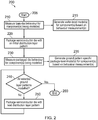
Figure 2 illustrates a simplified flowchart of an example embodiment of a method of model generation for use during the design and fabrication of integrated circuit device. -
Figure 3 schematically illustrates a simplified cross-sectional view of a part of a bare-mounted semiconductor die. -
Figures 4 to 10 schematically illustrate simplified cross-sectional views of parts of integrated circuit devices comprising equivalent packaged semiconductor dies comprising an inductive and/or a capacitive component being modelled with different package distribution layer patterns. -
Figure 11 schematically illustrates a simplified cross-sectional view of an integrated circuit device comprising packaged semiconductor die having multiple inductive components and different package distribution layer patterns. - Example embodiments of the present invention will now be described with reference to the accompanying drawings. However, it will be appreciated that the present invention is not limited to the specific examples herein described and as illustrated in the accompanying drawings.
- RF and millimetre-wave circuit design suffers from insufficient accuracy due to complicated parasitic capacitive and inductive influences. It is difficult to design a circuit to meet desired specifications by way of simulation alone. Specifically, the model of capacitive and inductive elements such as transmission lines, inductors, transformers, etc. is generally not accurate enough in RF and millimetre-wave circuit design, causing difficulties in designing accurate passive circuits such as passive filters, passive power dividers, and passive resonators, or even active circuits such as oscillators which use LC tank resonators. As such, simple and effective post-processing adjustment of capacitive and inductive values is expected to trim the circuit performance.
- Conventional post-trimming can only be done for transmission lines by changing the length of the transmission line. For spiral inductors and transformers it is very difficult to have a useful trimming model, especially within integrated circuits. As a result, spiral inductors and transformers can typically not be trimmed by post-processing in integrated circuit designs. Therefore, if the desired IC performance cannot be achieved, complete redesign is necessary. Furthermore, such conventional back-end techniques require at least one month and additional procedures to complete the re-optimized design and wafer back-end re-production, which adds a significant delay in the overall design cycle for the integrated circuit.
- In accordance with some example embodiments, there is proposed a method of tuning inductive and/or capacitive components within an integrated circuit device comprising measuring bare-die mounted performance of one or more component(s) formed within a semiconductor die, determining a package distribution layer pattern for the, or each, component for achieving a desired performance for the component(s) based at least partly on the measured bare-die mounted performance, and packaging the semiconductor die with the determined package distribution layer pattern.
- In this manner, any unexpected performance due to parasitic capacitive and/or inductive influences can be compensated for by way of the package distribution layer pattern on the surface top, such as described in greater detail below. As a result, inductive and capacitive components within a semiconductor die can be tuned using the package distribution layer pattern, and thus without the need for re-producing a new wafer during back-end adjustment. Advantageously, such a method of tuning inductive/capacitive components within an integrated circuit device significantly reduces the delay in the overall design cycle as compared with conventional techniques, and provides a practical tuning method for not only transmission lines as usual, but also spiral inductors, transformers, etc. that are difficult to tune within integrated circuit devices using conventional techniques.
- In accordance with some example embodiments, the proposed method may comprise adjusting a distance of package distribution layer pattern to the surface and/or an overlapping coverage of one or more package ground layers to the component being tuned and/or the thickness of the package ground layers(s) overlapping the component being tuned, which can effectively tune the inductive and/or capacitive component values. In order to make the performance trimming more predictable, a design PDK (process design kit) for all capacitive and inductive tuneable components such as transmission lines, inductances, capacitors, transformers, etc. may be created at wafer level and also at package level. Such a PDK generation is well known in semiconductor industry on wafer level, and typically comprises a measurement and modelling process of components on wafer. In some example embodiments it is contemplated that such a PDK can be enhanced to the package level by a measurement and modelling process on package for each tuneable component with different package distribution layer patterns as described in greater detail below.
-
Figure 1 illustrates asimplified flowchart 100 of an example of a method of tuning capacitive and inductive components within an integrated circuit device. The method ofFigure 1 starts at 105 and moves on to 110 where a radio-frequency (RF) or millimetre-wave (mm-wave) circuit is designed for an initial package distribution layer pattern. For example, such a circuit design may be performed by way of an electronic design automation (EDA) process, and may involve one or more of: - Design flow (for example comprising high-level and logical synthesis, component placement and layout, etc.);
- simulation (for example comprising transistor and logic simulation, high-level (behavioural) simulation, electromagnetic field solving, etc.); and
- Analysis and verification (for example comprising functional verification, clock domain crossing verification, equivalence checking, static timing analysis, etc.).
- In the illustrated example, the layout and design of capacitive and inductive components are designed for an integrated circuit (IC) based on package-level models for capacitance and inductance, which include wafer-level and package-level models, may be derived as described in greater detail with reference to
Figure 2 . The circuit typically includes not only capacitive and/or inductive components, but also other types of components such as CMOS (complementary metal-oxide semiconductor) components, HBT (Heterojunction Bipolar Transistor) components, resistors, etc. may be designed and optimized based on initial package-level models,and simulated performance by using wafer-level models as a comparable performance reference with the optimized performance . A wafer is then fabricated at 120 based on the designed layout. - Bare-die mounted IC performance for the fabricated wafer is then measured, at 130. In this manner, the wafer-level performance of the bare-die mounted IC may be obtained. The packaged IC performance with initial package distribution layer pattern can then be estimated based on a correlation between the measured wafer-level performance of the bare-die mounted IC and simulated wafer-level and package-level performance at 140. The wafer-level and package-level models may be derived as described in greater detail with reference to
Figure 2 . - Having estimated the packaged IC performance with the initial package distribution layer pattern, it is then determined whether the estimated packaged die performance achieves a desired IC performance, at 150.
- If it is determined that the estimated packaged die performance does not achieve the desired performance, the method of
Figure 1 moves on to 170 where package ground layer adjustments are determined, for example through simulation based on package-level models, to fine-tune inductive/capacitive components within the semiconductor die in order to achieve the desired IC performance. Such adjustments may comprise, for example, ground layer thickness, distance between ground layer and semiconductor die surface, ground layer overlap of inductive/capacitive component, etc. The tuneable capacitive/inductive components may comprise, for example, inductors, capacitors, transmission lines and transmission line based devices such as couplers, transformers, etc. Notably, transmission lines, which can be used as inductances or capacitances in RF and mm-wave circuits, have the most effective tuning capacity by changing the package distribution layer pattern on its surface. An example explanation of how a transmission line may be fine-tuned by way of modification of the package ground layer is provided below with reference toFigures 12 to 14 . - Having determined the package ground layer adjustments at 170, the method of
Figure 1 moves on to 180 where the package distribution layer pattern is modified in accordance with the determined package ground layer adjustments in order to achieve the desired packaged IC performance by tuning the capacitive/inductive component(s) and the semiconductor die is packaged with the modified distribution layer pattern. The performance of the packaged semiconductor die is then measured, at 185, and it is determined whether the packaged semiconductor die achieves the desired IC performance at 190 based on the measured performance. If it is determined that the packaged semiconductor die achieves the desired performance, the method ends 195. Conversely, if it is determined that the packaged semiconductor die does not achieve the desired performance, the method ofFigure 1 loops back to 170 again further adjustments to the distribution layer pattern are determined to fine-tune the inductive/capacitive components within the semiconductor die in order to achieve the desired IC performance. - Referring back to 150, if it is determined that the estimated packaged die performance does achieve the desired performance, the method moves on to 160 where the semiconductor die is packaged with the initial distribution layer pattern. The performance of the packaged IC is then measured at 185 and checked at 190 to determine whether it achieves the desired IC performance.
- In some further embodiments, it is contemplated that the method may further comprise selecting an inter-layer dielectric material based at least partly on the measured bare-die mounted performance, and packaging the semiconductor die using the selected inter-layer dielectric material between the package re-distribution layers. In this manner, the permittivity of the dielectric material may also be modified in order to achieve a required performance of capacitive/inductive components within the semiconductor die.
- Referring now to
Figure 2 , there is illustrated asimplified flowchart 200 of an example embodiment of a method of model generation for use during the design and optimization of integrated circuit devices. The method ofFigure 2 starts at 205 and moves on to 210, where bare-die behaviour for each individual component being modelled is measured.Figure 3 schematically illustrates a simplified cross-sectional view of a part of a bare-mounted semiconductor die 300 comprising acomponent 310 being modelled formed within an interlayer dielectric material (from silicon dioxides to newer low-K insulators) 320, and asubstrate 330 on the bottom. By measuring the bare-die behaviour of thecomponent 310, a wafer-level model for the fundamental component can be generated, as illustrated at 215 inFigure 2 . The components being modelled may comprise, for example, capacitive and inductive devices such as transmission lines, inductors, transformers, etc., as well as other types of components such as CMOS components, HBT components, resistors, etc. The wafer-level models may form part of a wafer-level process design kit (PDK) for the IC design. - Referring back to
Figure 2 , having measured the bare-die behaviour and generated the wafer-level model(s), the method moves on to 220 where in the illustrated example a semiconductor die comprising the component(s) being modelled are packaged with an initial ground layer patter. For example, the semiconductor die may be packaged with an outmost redistribution layer providing an overlying ground layer, for example as illustrated inFigure 4 . InFigure 4 , thedistribution layer pattern 340 comprises an outermost re-distribution layer (RDL) 342 overlapping therespective component 310 being modelled within the semiconductor die 400. Alternatively, and as illustrated inFigure 5 , thedistribution layer pattern 342 may comprise anoutermost RDL 340 that partially overlaps therespective component 310 being modelled within the semiconductor die 500. Adielectric material 350 is used to fill the space between the semiconductor die 400 - 1000 and the package ground layers 342. - Referring back to
Figure 2 , the packaged behaviour for each individual component being modelled is then measured, at 230, and a distribution layer pattern specific package-level model for the packaged component(s) is generated, as illustrated at 235. As previously described, the inductive and capacitive values of packaged components are heavily depended on the overlying distribution layer pattern and its overlap area. Accordingly, in the example illustrated inFigure 2 , packaged behaviour for the component(s) being modelled is measured for a plurality of different package distribution layer patterns and corresponding package-level models generated withinsteps 230 to 250. - For example,
Figures 4 to 10 schematically illustrate simplified cross-sectional views of integrated circuit devices comprising equivalent packaged semiconductor dies 600 - 1000 comprising theinductive component 310 being modelled with different package distribution layer patterns. In the examples illustrated inFigures 6 to 10 , the packagedistribution layer pattern 340 comprises a top-level ground layer 342 formed by the outer re-distribution layer of the packaged semiconductor die 600 - 1100 (e.g. an outermost re-distribution layer), for example the top-level ground layer 342 comprising an overlying ground layer for the respective semiconductor die 600 - 1000 as a whole. InFigures 6 to 10 , the packagedistribution layer pattern 340 comprises afurther ground layer 344 formed by an inner re-distribution layer of the packaging. Thefurther ground layer 344 formed by the inner re-distribution layer may comprise a component specific ground layer arranged to at least partially overlap therespective component 310 being modelled, and may be shorted to the top-level ground layer 342 by way of a via 346 or the like. Adielectric material 350 is used to fill the space between the semiconductor die 600 - 1000 and the package ground layers 342, 344. - As illustrated in
Figures 4 to 10 , each of the packaged semiconductor dies 400 - 1000 is packaged with different packagedistribution layer patterns 340 for thecomponent 310 being modelled. For example, the different packagedistribution layer patterns 340 may comprise ground layers 342, 344 having different overlapping coverage over thecomponent 310 being modelled and being spaced at different distances from thecomponent 310 being modelled. For example, inFigures 6 and 7 the packagedistribution layer patterns 340 comprise further ground layers 344 comprising approximately 50% coverage of thecomponent 310, but formed within different re-distribution layers and thus spaced at different distances from thecomponent 310. In addition, the further ground layers 344 inFigures 8 and 9 comprise approximately 75% and 25% coverage respectively, whist thefurther ground layer 344 inFigure 10 comprises approximately 100% coverage and is formed within a still further re-distribution layer. - Thus, in this manner behaviour measurements for the
component 310 being modelled may be obtained for different packagedistribution layer patterns 340, whereby the different packagedistribution layer patterns 340 differ by way of, for example, a distance and/or an overlapping coverage of one or more package ground layers 342, 344 in relation to thecomponent 310 being modelled.. - In some further embodiments, it is contemplated that the method may further comprise obtaining performance measurements for the different package
distribution layer patterns 340 in relation to differentdielectric materials 350 having different relative permittivity characteristics between the semiconductor die and the package ground layers 342, 344. - Referring back to
Figure 2 , at 240, having not modelled all components for each possible distribution layer pattern with different distance and/or coverage to each component, the method moves on to 250 where the type of package ground pattern of each component to be modelled is changed and moves back to 230 for re-measurement and the corresponding modelling. In the illustrated example a package-level model is generated for the, or each, component being modelled based on the performance measurement for a possible distribution layer pattern. The obtained model can be used for example for simulating and estimating the packaged die performance at 140 and 170 inFigure 1 . In some example embodiments, such an initial package distribution layer pattern may comprises a ground layer formed within a middle package redistribution layer arranged to provide approximately 50% coverage of the component being modelled. For example, from the packagedistribution layer patterns 340 ofFigures 4 to 10 , the package distribution layer pattern illustrated inFigure 6 in which thefurther ground layer 344 comprises approximately 50% coverage of thecomponent 310 and is formed within the first (middle) re-distribution layer. In this manner, the tuning capabilities from modifying the package distribution layer pattern are optimized in each direction (i.e. for increasing and decreasing the parasitic capacitive effects of the packaging. - Referring back to
Figure 2 , once package-level models have been generated for each intended distribution layer pattern, then method ends at 260. -
Figure 11 schematically illustrates a simplified cross-sectional view of an integrated circuit device comprising packaged semiconductor die 1100 having multipleinductive components Figure 11 , the packaged semiconductor die 1100 comprises a first package distribution layer pattern provided above a firstinductive component 1110. The first package distribution layer pattern comprises a top-level ground layer 1142 formed by an outer re-distribution layer of the packaged semiconductor die 1100. For example, the top-level ground layer 1142 may comprise an overlying ground layer for the respective semiconductor die 1100 as a whole. The first package distribution layer pattern comprises a firstfurther ground layer 1144 formed by a first inner re-distribution layer of the packaging. In the illustrated example, the firstfurther ground layer 1144 formed by the inner re-distribution layer is arranged to provide approximately 100% coverage of thefirst component 1110, and is coupled to the top-level ground layer 1142 by way of a via. In the example illustrated inFigure 11 , the packaged semiconductor die 1100 comprises a second package distribution layer pattern provided above a secondinductive component 1115. The second package distribution layer pattern comprises the top-level ground layer 1142 formed by the outer re-distribution layer of the packaged semiconductor die 1100. The second package distribution layer pattern comprises a secondfurther ground layer 1148 formed by a second inner re-distribution layer of the packaging. In the illustrated example, the second further ground layer 1146 formed by the inner re-distribution layer is arranged to provide approximately 75% coverage of thesecond component 1115, and is coupled to the top-level ground layer 1142 by way of a via. Thus, it is contemplated that package distribution layer patterns may be individually adapted for each capacitive and/or inductive component within a semiconductor die. - An example explanation of how a transmission line may be fine-tuned by way of modification of the package ground layer will now be provided with reference to
Figures 12 to 14 . A general transmission line is illustrated inFigure 12 comprising atransmission line 310, a firstdielectric material 320, asubstrate 330, and aground layer 340 within the package filled by a furtherdielectric material 350 betweentransmission line 310 and thepackage ground layer 340. The characteristic impedance Zo and propagation constant γ can be expressed as below, respectively:

- R is the resistance per unit length, considering the two conductors to be in series, L is the inductance per unit length, G is the conductance of the dielectric per unit length, C is the capacitance per unit length, j is the imaginary unit, and ω is the angular frequency.
- The inductance and capacitance per unit length may be approximated to:


- Respectively, where µ is the conductor conductivity factor, ε is the permittivity of filled dielectric material between the transmission line, h is the distance between the ground layer and the transmission line, and w is the width of the transmission line.
- From Equations 3 and 4 the transmission line characterization parameters such as L, C, the effective permittivity the characteristic impedance and the propagation constant are dependent on the distance or/and the overlap coverage of the distribution layer pattern in relation to the transmission line. The change of characteristic impedance and the phase of the propagation of transmission line can be used to change the circuit performance, for example in relation to the frequency insertion loss, return loss and power loss, by adjusting the distribution layer pattern over the surface of the transmission line or/and transmission line based devices within the packaged IC.
- Moreover, a lossless input impedance of a transmission line can be expressed as:

- β: propagation of the transmission line, and I: length of transmission line, For a short circuit, as illustrated in
Figure 13 , the transmission line has a inductive impedance when the length of the transmission line is less than ¼ of the signal wavelength or between ¼ and ¾ the wavelength, and the equivalent inductance is:
- The transmission line has a capacitive impedance when the length of the transmission line is between ¼ and ½ of the signal wavelength or between ¾ and 1 wavelength. The equivalent capacitance can be expressed as:

- An open transmission line, as illustrated in
Figure 14 , can be treated as an inductance or a capacitance depended only on the length of transmission line in comparison with the length of wavelength. The inductive or capacitive impedance is similar as for a shorted transmission line circuit, which is depended only on the characteristic impedance and the phase of propagation of the transmission line. Whereas the characteristic impedance and the phase of propagation of the transmission line both can be changed by proposed post-processing the ground pattern over the transmission line. - Thus example embodiments of a method for tuning inductive and/or capacitive components within an integrated circuit device have been described using 'topside' ground patterns formed by on-wafer package redistribution layers. Notably, from Equation 1 above it can be seen that by changing the package distribution layer pattern over a component, the parasitic capacitance from the package distribution layer pattern can be modified, enabling the characteristic impedance of the component to be tuned over a wide range. For example, in the case of a transmission line (typically used to implement inductors within integrated circuits) having a length less than λ/4, the packaging effects the properties of the transmission line in two ways:
- (i) the characteristic impedance Z0; and
- (ii) the effective permittivity εeff of the dielectric material.
- For low frequencies, or shorter transmission line lengths, the characteristic impedance effects are dominant, reducing the inductance value. For higher frequencies or longer transmission line lengths, effective permittivity εeff of the dielectric material may compensate the characteristic impedance effects.
- In the foregoing specification, the invention has been described with reference to specific examples of embodiments of the invention. It will, however, be evident that various modifications and changes may be made therein without departing from the scope of the invention as set forth in the appended claims and that the claims are not limited to the specific examples described above.
- Furthermore, because the illustrated embodiments of the present invention may for the most part, be implemented using electronic components and circuits known to those skilled in the art, details will not be explained in any greater extent than that considered necessary as illustrated above, for the understanding and appreciation of the underlying concepts of the present invention and in order not to obfuscate or distract from the teachings of the present invention.
- For example, the semiconductor substrate described herein can be any semiconductor material or combinations of materials, such as gallium arsenide, silicon germanium, silicon-on-insulator (SOI), silicon, monocrystalline silicon, the like, and combinations of the above.
- Moreover, the terms 'front,' 'back,' 'top,' 'bottom,' 'over,' 'under' and the like in the description and in the claims, if any, are used for descriptive purposes and not necessarily for describing permanent relative positions. It is understood that the terms so used are interchangeable under appropriate circumstances such that the embodiments of the invention described herein are, for example, capable of operation in other orientations than those illustrated or otherwise described herein.
- Any arrangement of components to achieve the same functionality is effectively 'associated' such that the desired functionality is achieved. Hence, any two components herein combined to achieve a particular functionality can be seen as 'associated with' each other such that the desired functionality is achieved, irrespective of architectures or intermediary components. Likewise, any two components so associated can also be viewed as being 'operably connected,' or 'operably coupled,' to each other to achieve the desired functionality.
- Furthermore, those skilled in the art will recognize that boundaries between the above described operations merely illustrative. The multiple operations may be combined into a single operation, a single operation may be distributed in additional operations and operations may be executed at least partially overlapping in time. Moreover, alternative embodiments may include multiple instances of a particular operation, and the order of operations may be altered in various other embodiments.
- However, other modifications, variations and alternatives are also possible. The specifications and drawings are, accordingly, to be regarded in an illustrative rather than in a restrictive sense.
- In the claims, any reference signs placed between parentheses shall not be construed as limiting the claim. The word 'comprising' does not exclude the presence of other elements or steps then those listed in a claim. Furthermore, the terms 'a' or 'an,' as used herein, are defined as one or more than one. Also, the use of introductory phrases such as 'at least one' and 'one or more' in the claims should not be construed to imply that the introduction of another claim element by the indefinite articles 'a' or 'an' limits any particular claim containing such introduced claim element to inventions containing only one such element, even when the same claim includes the introductory phrases 'one or more' or 'at least one' and indefinite articles such as 'a' or 'an.' The same holds true for the use of definite articles. Unless stated otherwise, terms such as 'first' and 'second' are used to arbitrarily distinguish between the elements such terms describe. Thus, these terms are not necessarily intended to indicate temporal or other prioritization of such elements. The mere fact that certain measures are recited in mutually different claims does not indicate that a combination of these measures cannot be used to advantage.
Claims (10)
- A method of tuning at least one of inductive and capacitive components within an integrated circuit device; the method comprising:measuring bare-die mounted performance of at least one component formed within a semiconductor die;determining a package distribution layer pattern for the at least one component for achieving a desired performance for the at least one component based at least partly on the measured bare-die mounted performance; andpackaging the semiconductor die with the determined package distribution layer pattern for the at least one component.
- The method of Claim 1, wherein the method comprises:estimating a packaged die performance for the at least one component for an initial package distribution layer pattern based at least partly on the measured bare-die mounted performance;determining whether the estimated packaged die performance achieves the desired performance for the at least one component; andif it is determined that the estimated packaged die performance does not achieve the desired performance, modifying the distribution layer pattern for the at least one component to achieve the desired packaged performance.
- The method of Claim 2, wherein if it is determined that the estimated performance for the at least one component does not achieve the desired packaged performance for the at least one component, the method further comprises:determining ground layer adjustments for achieving the desired packaged performance for the at least one component; andmodifying the package distribution layer pattern for the at least one component based at least partly on the determined ground layer adjustments.
- The method of Claim 2 or Claim 3, wherein the estimated performance for the at least one component is determined based at least partly on pre-defined package-level models of component performance in relation to different package distribution layer patterns.
- The method of Claim 4, wherein the method further comprises generating package-level models corresponding to the at least one component; the method comprising:measuring bare-die mounted behaviour for the at least one component to be modelled;measuring packaged behaviour for the at least one component for a plurality of package distribution layer patterns; andgenerating package-level models for the at least one component based on the measured bare-die and packaged behaviours for the at least one component.
- The method of any one of Claims 2 to 5, wherein modifying the distribution layer pattern for the at least one component comprises at least one of:modifying an overlapping coverage of at least one package ground layer over the at least one component; andchanging a package redistribution layer used for forming the at least one package ground layer over the at least one component.
- The method of any one of Claims 2 to 6, wherein the initial package distribution layer pattern comprises a ground layer formed within a middle package redistribution layer arranged to provide 50% coverage of the at least one component.
- The method of any one of the preceding Claims, wherein the method comprises designing a wafer layout for the semiconductor die based at least partly on wafer-level models for the at least one component.
- The method of any one of the preceding Claims, where the method further comprises selecting an inter-layer dielectric material based at least partly on the measured bare-die mounted performance, and packaging the semiconductor die with the selected inter-layer dielectric material.
- An integrated circuit device comprising at least one packaged semiconductor die comprising at least one component tuned in accordance with the method of any one of the preceding Claims.
Priority Applications (2)
| Application Number | Priority Date | Filing Date | Title |
|---|---|---|---|
| EP16206605.4A EP3340082B1 (en) | 2016-12-23 | 2016-12-23 | Method of tuning components within an integrated circuit device |
| US15/833,033 US10522458B2 (en) | 2016-12-23 | 2017-12-06 | Method of tuning components within an integracted circuit device |
Applications Claiming Priority (1)
| Application Number | Priority Date | Filing Date | Title |
|---|---|---|---|
| EP16206605.4A EP3340082B1 (en) | 2016-12-23 | 2016-12-23 | Method of tuning components within an integrated circuit device |
Publications (2)
| Publication Number | Publication Date |
|---|---|
| EP3340082A1 true EP3340082A1 (en) | 2018-06-27 |
| EP3340082B1 EP3340082B1 (en) | 2021-02-17 |
Family
ID=57755045
Family Applications (1)
| Application Number | Title | Priority Date | Filing Date |
|---|---|---|---|
| EP16206605.4A Active EP3340082B1 (en) | 2016-12-23 | 2016-12-23 | Method of tuning components within an integrated circuit device |
Country Status (2)
| Country | Link |
|---|---|
| US (1) | US10522458B2 (en) |
| EP (1) | EP3340082B1 (en) |
Families Citing this family (1)
| Publication number | Priority date | Publication date | Assignee | Title |
|---|---|---|---|---|
| JP7632219B2 (en) * | 2021-10-05 | 2025-02-19 | 住友電気工業株式会社 | High Frequency Device |
Citations (5)
| Publication number | Priority date | Publication date | Assignee | Title |
|---|---|---|---|---|
| US20040000970A1 (en) * | 2002-06-27 | 2004-01-01 | Killen William D. | High efficiency coupled line filters |
| US20080030280A1 (en) * | 2005-04-13 | 2008-02-07 | Floyd Brian A | Circuits and Methods for Implementing Transformer-Coupled Amplifiers at Millimeter Wave Frequencies |
| US20090236701A1 (en) * | 2008-03-18 | 2009-09-24 | Nanyang Technological University | Chip arrangement and a method of determining an inductivity compensation structure for compensating a bond wire inductivity in a chip arrangement |
| US20140310671A1 (en) * | 2013-04-16 | 2014-10-16 | Infineon Technologies Ag | Electrical Measurement Based Circuit Wiring Layout Modification Method and System |
| US20160190673A1 (en) * | 2014-12-24 | 2016-06-30 | Nxp B.V. | Ic-package interconnect for millimeter wave systems |
Family Cites Families (17)
| Publication number | Priority date | Publication date | Assignee | Title |
|---|---|---|---|---|
| US3947934A (en) | 1973-07-20 | 1976-04-06 | Rca Corporation | Method of tuning a tunable microelectronic LC circuit |
| JPH04117805A (en) | 1990-09-07 | 1992-04-17 | Matsushita Electric Ind Co Ltd | High frequency voltage controlled oscillator |
| US5701032A (en) * | 1994-10-17 | 1997-12-23 | W. L. Gore & Associates, Inc. | Integrated circuit package |
| US6181225B1 (en) | 1998-02-17 | 2001-01-30 | Itron, Inc. | Laser tunable thick film microwave resonator for printed circuit boards |
| US6189201B1 (en) | 1999-03-19 | 2001-02-20 | Sino Dragon Inc. | Method of tuning a high frequency printed resonance circuit |
| US7135344B2 (en) * | 2003-07-11 | 2006-11-14 | Applied Materials, Israel, Ltd. | Design-based monitoring |
| US8286111B2 (en) * | 2004-03-11 | 2012-10-09 | Gradient Design Automation Inc. | Thermal simulation using adaptive 3D and hierarchical grid mechanisms |
| US7774625B1 (en) * | 2004-06-22 | 2010-08-10 | Eric Chien-Li Sheng | Adaptive voltage control by accessing information stored within and specific to a microprocessor |
| US7239163B1 (en) * | 2004-06-23 | 2007-07-03 | Ridgetop Group, Inc. | Die-level process monitor and method |
| EP1960921A1 (en) * | 2005-12-17 | 2008-08-27 | Gradient Design Automation, Inc. | Simulation of ic temperature distributions using an adaptive 3d grid |
| US20090030660A1 (en) * | 2007-07-24 | 2009-01-29 | Lsi Logic Corporation | Method and apparatus for generating fully detailed three-dimensional electronic package and pcb board models |
| US20100068831A1 (en) * | 2008-09-12 | 2010-03-18 | Skyworks Solutions, Inc. | Method for wafer trimming for increased device yield |
| US8204721B2 (en) * | 2009-06-29 | 2012-06-19 | Sentinel Ic Technologies, Inc. | Apparatus and method for emulation of process variation induced in split process semiconductor wafers |
| US8254200B2 (en) * | 2009-09-11 | 2012-08-28 | Sherif Eid | System and method to compensate for process and environmental variations in semiconductor devices |
| US8912809B2 (en) * | 2012-06-12 | 2014-12-16 | Apple Inc. | Methods and apparatus for performing wafer-level testing on antenna tuning elements |
| US9740815B2 (en) * | 2015-10-26 | 2017-08-22 | Globalfoundries Inc. | Electromigration-aware integrated circuit design methods and systems |
| US10635771B2 (en) * | 2017-10-18 | 2020-04-28 | Anaglobe Technology, Inc. | Method for parasitic-aware capacitor sizing and layout generation |
-
2016
- 2016-12-23 EP EP16206605.4A patent/EP3340082B1/en active Active
-
2017
- 2017-12-06 US US15/833,033 patent/US10522458B2/en active Active
Patent Citations (5)
| Publication number | Priority date | Publication date | Assignee | Title |
|---|---|---|---|---|
| US20040000970A1 (en) * | 2002-06-27 | 2004-01-01 | Killen William D. | High efficiency coupled line filters |
| US20080030280A1 (en) * | 2005-04-13 | 2008-02-07 | Floyd Brian A | Circuits and Methods for Implementing Transformer-Coupled Amplifiers at Millimeter Wave Frequencies |
| US20090236701A1 (en) * | 2008-03-18 | 2009-09-24 | Nanyang Technological University | Chip arrangement and a method of determining an inductivity compensation structure for compensating a bond wire inductivity in a chip arrangement |
| US20140310671A1 (en) * | 2013-04-16 | 2014-10-16 | Infineon Technologies Ag | Electrical Measurement Based Circuit Wiring Layout Modification Method and System |
| US20160190673A1 (en) * | 2014-12-24 | 2016-06-30 | Nxp B.V. | Ic-package interconnect for millimeter wave systems |
Non-Patent Citations (1)
| Title |
|---|
| STARZER F ET AL: "A low phase noise VCO in eWLB package", ELECTRONICS PACKAGING TECHNOLOGY CONFERENCE (EPTC), 2012 IEEE 14TH, IEEE, 5 December 2012 (2012-12-05), pages 326 - 329, XP032426044, ISBN: 978-1-4673-4553-8, DOI: 10.1109/EPTC.2012.6507101 * |
Also Published As
| Publication number | Publication date |
|---|---|
| US10522458B2 (en) | 2019-12-31 |
| EP3340082B1 (en) | 2021-02-17 |
| US20180182705A1 (en) | 2018-06-28 |
Similar Documents
| Publication | Publication Date | Title |
|---|---|---|
| Tiemeijer et al. | A calibrated lumped-element de-embedding technique for on-wafer RF characterization of high-quality inductors and high-speed transistors | |
| CN103050479B (en) | Method and apparatus for de-embedding | |
| Gao et al. | Scalable compact circuit model and synthesis for RF CMOS spiral inductors | |
| CN101501691B (en) | Circuit simulator parameter extraction using a configurable ring oscillator | |
| US9576915B2 (en) | IC-package interconnect for millimeter wave systems | |
| Liu et al. | A broadband model over 1–220 GHz for GSG pad structures in RF CMOS | |
| Johansen et al. | EM simulation accuracy enhancement for broadband modeling of on-wafer passive components | |
| US20080177514A1 (en) | Method for modeling varactor by direct extraction of parameters | |
| US10522458B2 (en) | Method of tuning components within an integracted circuit device | |
| US7949975B2 (en) | Apparatus and method of extracting equivalent circuit of T-type transmission circuit | |
| Goto et al. | New on-chip de-embedding for accurate evaluation of symmetric devices | |
| Valdés-Rayón et al. | Modeling ground-shielded integrated inductors incorporating frequency-dependent effects and considering multiple resonances | |
| Royet et al. | Experimental and simulation results on Si integrated inductor efficiency for smart RF-ICs | |
| Jeong et al. | Modeling of T-model equivalent circuit for spiral inductors in 90 nm CMOS technology | |
| Su et al. | A macro model of silicon spiral inductor | |
| Valdés-Rayón et al. | Determination of the contribution of the ground-shield losses to the microwave performance of on-chip coplanar waveguides | |
| Scheir et al. | Design and analysis of inductors for 60 GHz applications in a digital CMOS technology | |
| Okada et al. | Modelling and optimization of on-chip spiral inductor in S-parameter domain | |
| Dinh et al. | Modeling and characterization of bond-wire arrays for distributed Chip-Package-PCB Co-design | |
| Mukhtar et al. | Variation-aware X-topology architecture with local ground references for broadband characterization of passives | |
| Shu et al. | Characterization of LC-tank circuits for mm-wave applications in 90 nm CMOS | |
| Lourandakis et al. | Integrated RF transformer and power combiner design in 150nm CMOS process | |
| Gao et al. | An improved equivalent circuit model based on the CMOS on-chip multiple coupled inductors from DC to millimeter-wave region | |
| Wane et al. | Topological and functional partitioning in EM analysis: Application to wafer-level chip-scale harmonic filters | |
| Wang et al. | Analysis and modelling on CMOS spiral inductor with impact of metal dummy fills |
Legal Events
| Date | Code | Title | Description |
|---|---|---|---|
| PUAI | Public reference made under article 153(3) epc to a published international application that has entered the european phase |
Free format text: ORIGINAL CODE: 0009012 |
|
| STAA | Information on the status of an ep patent application or granted ep patent |
Free format text: STATUS: THE APPLICATION HAS BEEN PUBLISHED |
|
| AK | Designated contracting states |
Kind code of ref document: A1 Designated state(s): AL AT BE BG CH CY CZ DE DK EE ES FI FR GB GR HR HU IE IS IT LI LT LU LV MC MK MT NL NO PL PT RO RS SE SI SK SM TR |
|
| AX | Request for extension of the european patent |
Extension state: BA ME |
|
| STAA | Information on the status of an ep patent application or granted ep patent |
Free format text: STATUS: REQUEST FOR EXAMINATION WAS MADE |
|
| 17P | Request for examination filed |
Effective date: 20190102 |
|
| RBV | Designated contracting states (corrected) |
Designated state(s): AL AT BE BG CH CY CZ DE DK EE ES FI FR GB GR HR HU IE IS IT LI LT LU LV MC MK MT NL NO PL PT RO RS SE SI SK SM TR |
|
| STAA | Information on the status of an ep patent application or granted ep patent |
Free format text: STATUS: EXAMINATION IS IN PROGRESS |
|
| 17Q | First examination report despatched |
Effective date: 20200122 |
|
| RIC1 | Information provided on ipc code assigned before grant |
Ipc: G06F 113/18 20200101ALN20200727BHEP Ipc: H01L 23/522 20060101ALI20200727BHEP Ipc: G06F 119/10 20200101ALN20200727BHEP Ipc: G06F 119/12 20200101ALN20200727BHEP Ipc: H01L 23/64 20060101ALN20200727BHEP Ipc: G06F 30/39 20200101AFI20200727BHEP |
|
| REG | Reference to a national code |
Ref country code: DE Ref legal event code: R079 Ref document number: 602016052508 Country of ref document: DE Free format text: PREVIOUS MAIN CLASS: G06F0017500000 Ipc: G06F0030390000 |
|
| GRAP | Despatch of communication of intention to grant a patent |
Free format text: ORIGINAL CODE: EPIDOSNIGR1 |
|
| STAA | Information on the status of an ep patent application or granted ep patent |
Free format text: STATUS: GRANT OF PATENT IS INTENDED |
|
| RIC1 | Information provided on ipc code assigned before grant |
Ipc: G06F 119/12 20200101ALN20200923BHEP Ipc: G06F 30/39 20200101AFI20200923BHEP Ipc: H01L 23/522 20060101ALI20200923BHEP Ipc: G06F 119/10 20200101ALN20200923BHEP Ipc: G06F 113/18 20200101ALN20200923BHEP Ipc: H01L 23/64 20060101ALN20200923BHEP |
|
| INTG | Intention to grant announced |
Effective date: 20201023 |
|
| GRAS | Grant fee paid |
Free format text: ORIGINAL CODE: EPIDOSNIGR3 |
|
| GRAA | (expected) grant |
Free format text: ORIGINAL CODE: 0009210 |
|
| STAA | Information on the status of an ep patent application or granted ep patent |
Free format text: STATUS: THE PATENT HAS BEEN GRANTED |
|
| AK | Designated contracting states |
Kind code of ref document: B1 Designated state(s): AL AT BE BG CH CY CZ DE DK EE ES FI FR GB GR HR HU IE IS IT LI LT LU LV MC MK MT NL NO PL PT RO RS SE SI SK SM TR |
|
| REG | Reference to a national code |
Ref country code: GB Ref legal event code: FG4D |
|
| REG | Reference to a national code |
Ref country code: CH Ref legal event code: EP |
|
| REG | Reference to a national code |
Ref country code: DE Ref legal event code: R096 Ref document number: 602016052508 Country of ref document: DE |
|
| REG | Reference to a national code |
Ref country code: AT Ref legal event code: REF Ref document number: 1362429 Country of ref document: AT Kind code of ref document: T Effective date: 20210315 |
|
| REG | Reference to a national code |
Ref country code: IE Ref legal event code: FG4D |
|
| REG | Reference to a national code |
Ref country code: LT Ref legal event code: MG9D |
|
| REG | Reference to a national code |
Ref country code: NL Ref legal event code: MP Effective date: 20210217 |
|
| PG25 | Lapsed in a contracting state [announced via postgrant information from national office to epo] |
Ref country code: PT Free format text: LAPSE BECAUSE OF FAILURE TO SUBMIT A TRANSLATION OF THE DESCRIPTION OR TO PAY THE FEE WITHIN THE PRESCRIBED TIME-LIMIT Effective date: 20210617 Ref country code: NO Free format text: LAPSE BECAUSE OF FAILURE TO SUBMIT A TRANSLATION OF THE DESCRIPTION OR TO PAY THE FEE WITHIN THE PRESCRIBED TIME-LIMIT Effective date: 20210517 Ref country code: FI Free format text: LAPSE BECAUSE OF FAILURE TO SUBMIT A TRANSLATION OF THE DESCRIPTION OR TO PAY THE FEE WITHIN THE PRESCRIBED TIME-LIMIT Effective date: 20210217 Ref country code: GR Free format text: LAPSE BECAUSE OF FAILURE TO SUBMIT A TRANSLATION OF THE DESCRIPTION OR TO PAY THE FEE WITHIN THE PRESCRIBED TIME-LIMIT Effective date: 20210518 Ref country code: HR Free format text: LAPSE BECAUSE OF FAILURE TO SUBMIT A TRANSLATION OF THE DESCRIPTION OR TO PAY THE FEE WITHIN THE PRESCRIBED TIME-LIMIT Effective date: 20210217 Ref country code: LT Free format text: LAPSE BECAUSE OF FAILURE TO SUBMIT A TRANSLATION OF THE DESCRIPTION OR TO PAY THE FEE WITHIN THE PRESCRIBED TIME-LIMIT Effective date: 20210217 Ref country code: BG Free format text: LAPSE BECAUSE OF FAILURE TO SUBMIT A TRANSLATION OF THE DESCRIPTION OR TO PAY THE FEE WITHIN THE PRESCRIBED TIME-LIMIT Effective date: 20210517 |
|
| REG | Reference to a national code |
Ref country code: AT Ref legal event code: MK05 Ref document number: 1362429 Country of ref document: AT Kind code of ref document: T Effective date: 20210217 |
|
| PG25 | Lapsed in a contracting state [announced via postgrant information from national office to epo] |
Ref country code: SE Free format text: LAPSE BECAUSE OF FAILURE TO SUBMIT A TRANSLATION OF THE DESCRIPTION OR TO PAY THE FEE WITHIN THE PRESCRIBED TIME-LIMIT Effective date: 20210217 Ref country code: RS Free format text: LAPSE BECAUSE OF FAILURE TO SUBMIT A TRANSLATION OF THE DESCRIPTION OR TO PAY THE FEE WITHIN THE PRESCRIBED TIME-LIMIT Effective date: 20210217 Ref country code: NL Free format text: LAPSE BECAUSE OF FAILURE TO SUBMIT A TRANSLATION OF THE DESCRIPTION OR TO PAY THE FEE WITHIN THE PRESCRIBED TIME-LIMIT Effective date: 20210217 Ref country code: PL Free format text: LAPSE BECAUSE OF FAILURE TO SUBMIT A TRANSLATION OF THE DESCRIPTION OR TO PAY THE FEE WITHIN THE PRESCRIBED TIME-LIMIT Effective date: 20210217 Ref country code: LV Free format text: LAPSE BECAUSE OF FAILURE TO SUBMIT A TRANSLATION OF THE DESCRIPTION OR TO PAY THE FEE WITHIN THE PRESCRIBED TIME-LIMIT Effective date: 20210217 |
|
| PG25 | Lapsed in a contracting state [announced via postgrant information from national office to epo] |
Ref country code: IS Free format text: LAPSE BECAUSE OF FAILURE TO SUBMIT A TRANSLATION OF THE DESCRIPTION OR TO PAY THE FEE WITHIN THE PRESCRIBED TIME-LIMIT Effective date: 20210617 |
|
| PG25 | Lapsed in a contracting state [announced via postgrant information from national office to epo] |
Ref country code: CZ Free format text: LAPSE BECAUSE OF FAILURE TO SUBMIT A TRANSLATION OF THE DESCRIPTION OR TO PAY THE FEE WITHIN THE PRESCRIBED TIME-LIMIT Effective date: 20210217 Ref country code: EE Free format text: LAPSE BECAUSE OF FAILURE TO SUBMIT A TRANSLATION OF THE DESCRIPTION OR TO PAY THE FEE WITHIN THE PRESCRIBED TIME-LIMIT Effective date: 20210217 Ref country code: SM Free format text: LAPSE BECAUSE OF FAILURE TO SUBMIT A TRANSLATION OF THE DESCRIPTION OR TO PAY THE FEE WITHIN THE PRESCRIBED TIME-LIMIT Effective date: 20210217 Ref country code: AT Free format text: LAPSE BECAUSE OF FAILURE TO SUBMIT A TRANSLATION OF THE DESCRIPTION OR TO PAY THE FEE WITHIN THE PRESCRIBED TIME-LIMIT Effective date: 20210217 |
|
| REG | Reference to a national code |
Ref country code: DE Ref legal event code: R097 Ref document number: 602016052508 Country of ref document: DE |
|
| PG25 | Lapsed in a contracting state [announced via postgrant information from national office to epo] |
Ref country code: SK Free format text: LAPSE BECAUSE OF FAILURE TO SUBMIT A TRANSLATION OF THE DESCRIPTION OR TO PAY THE FEE WITHIN THE PRESCRIBED TIME-LIMIT Effective date: 20210217 Ref country code: RO Free format text: LAPSE BECAUSE OF FAILURE TO SUBMIT A TRANSLATION OF THE DESCRIPTION OR TO PAY THE FEE WITHIN THE PRESCRIBED TIME-LIMIT Effective date: 20210217 Ref country code: DK Free format text: LAPSE BECAUSE OF FAILURE TO SUBMIT A TRANSLATION OF THE DESCRIPTION OR TO PAY THE FEE WITHIN THE PRESCRIBED TIME-LIMIT Effective date: 20210217 |
|
| PLBE | No opposition filed within time limit |
Free format text: ORIGINAL CODE: 0009261 |
|
| STAA | Information on the status of an ep patent application or granted ep patent |
Free format text: STATUS: NO OPPOSITION FILED WITHIN TIME LIMIT |
|
| 26N | No opposition filed |
Effective date: 20211118 |
|
| PG25 | Lapsed in a contracting state [announced via postgrant information from national office to epo] |
Ref country code: ES Free format text: LAPSE BECAUSE OF FAILURE TO SUBMIT A TRANSLATION OF THE DESCRIPTION OR TO PAY THE FEE WITHIN THE PRESCRIBED TIME-LIMIT Effective date: 20210217 Ref country code: AL Free format text: LAPSE BECAUSE OF FAILURE TO SUBMIT A TRANSLATION OF THE DESCRIPTION OR TO PAY THE FEE WITHIN THE PRESCRIBED TIME-LIMIT Effective date: 20210217 |
|
| PG25 | Lapsed in a contracting state [announced via postgrant information from national office to epo] |
Ref country code: SI Free format text: LAPSE BECAUSE OF FAILURE TO SUBMIT A TRANSLATION OF THE DESCRIPTION OR TO PAY THE FEE WITHIN THE PRESCRIBED TIME-LIMIT Effective date: 20210217 |
|
| PG25 | Lapsed in a contracting state [announced via postgrant information from national office to epo] |
Ref country code: IT Free format text: LAPSE BECAUSE OF FAILURE TO SUBMIT A TRANSLATION OF THE DESCRIPTION OR TO PAY THE FEE WITHIN THE PRESCRIBED TIME-LIMIT Effective date: 20210217 |
|
| PG25 | Lapsed in a contracting state [announced via postgrant information from national office to epo] |
Ref country code: IS Free format text: LAPSE BECAUSE OF FAILURE TO SUBMIT A TRANSLATION OF THE DESCRIPTION OR TO PAY THE FEE WITHIN THE PRESCRIBED TIME-LIMIT Effective date: 20210617 |
|
| PG25 | Lapsed in a contracting state [announced via postgrant information from national office to epo] |
Ref country code: MC Free format text: LAPSE BECAUSE OF FAILURE TO SUBMIT A TRANSLATION OF THE DESCRIPTION OR TO PAY THE FEE WITHIN THE PRESCRIBED TIME-LIMIT Effective date: 20210217 |
|
| REG | Reference to a national code |
Ref country code: CH Ref legal event code: PL |
|
| GBPC | Gb: european patent ceased through non-payment of renewal fee |
Effective date: 20211223 |
|
| REG | Reference to a national code |
Ref country code: BE Ref legal event code: MM Effective date: 20211231 |
|
| PG25 | Lapsed in a contracting state [announced via postgrant information from national office to epo] |
Ref country code: LU Free format text: LAPSE BECAUSE OF NON-PAYMENT OF DUE FEES Effective date: 20211223 Ref country code: IE Free format text: LAPSE BECAUSE OF NON-PAYMENT OF DUE FEES Effective date: 20211223 Ref country code: GB Free format text: LAPSE BECAUSE OF NON-PAYMENT OF DUE FEES Effective date: 20211223 |
|
| PG25 | Lapsed in a contracting state [announced via postgrant information from national office to epo] |
Ref country code: FR Free format text: LAPSE BECAUSE OF NON-PAYMENT OF DUE FEES Effective date: 20211231 Ref country code: BE Free format text: LAPSE BECAUSE OF NON-PAYMENT OF DUE FEES Effective date: 20211231 |
|
| PG25 | Lapsed in a contracting state [announced via postgrant information from national office to epo] |
Ref country code: LI Free format text: LAPSE BECAUSE OF NON-PAYMENT OF DUE FEES Effective date: 20211231 Ref country code: CH Free format text: LAPSE BECAUSE OF NON-PAYMENT OF DUE FEES Effective date: 20211231 |
|
| PG25 | Lapsed in a contracting state [announced via postgrant information from national office to epo] |
Ref country code: HU Free format text: LAPSE BECAUSE OF FAILURE TO SUBMIT A TRANSLATION OF THE DESCRIPTION OR TO PAY THE FEE WITHIN THE PRESCRIBED TIME-LIMIT; INVALID AB INITIO Effective date: 20161223 |
|
| PG25 | Lapsed in a contracting state [announced via postgrant information from national office to epo] |
Ref country code: CY Free format text: LAPSE BECAUSE OF FAILURE TO SUBMIT A TRANSLATION OF THE DESCRIPTION OR TO PAY THE FEE WITHIN THE PRESCRIBED TIME-LIMIT Effective date: 20210217 |
|
| P01 | Opt-out of the competence of the unified patent court (upc) registered |
Effective date: 20230725 |
|
| PG25 | Lapsed in a contracting state [announced via postgrant information from national office to epo] |
Ref country code: MK Free format text: LAPSE BECAUSE OF FAILURE TO SUBMIT A TRANSLATION OF THE DESCRIPTION OR TO PAY THE FEE WITHIN THE PRESCRIBED TIME-LIMIT Effective date: 20210217 |
|
| PG25 | Lapsed in a contracting state [announced via postgrant information from national office to epo] |
Ref country code: MT Free format text: LAPSE BECAUSE OF FAILURE TO SUBMIT A TRANSLATION OF THE DESCRIPTION OR TO PAY THE FEE WITHIN THE PRESCRIBED TIME-LIMIT Effective date: 20210217 |
|
| PG25 | Lapsed in a contracting state [announced via postgrant information from national office to epo] |
Ref country code: TR Free format text: LAPSE BECAUSE OF FAILURE TO SUBMIT A TRANSLATION OF THE DESCRIPTION OR TO PAY THE FEE WITHIN THE PRESCRIBED TIME-LIMIT Effective date: 20210217 |
|
| PGFP | Annual fee paid to national office [announced via postgrant information from national office to epo] |
Ref country code: DE Payment date: 20251126 Year of fee payment: 10 |