EP3336901A2 - Normally-off hemt with self-aligned gate structure - Google Patents
Normally-off hemt with self-aligned gate structure Download PDFInfo
- Publication number
- EP3336901A2 EP3336901A2 EP17201711.3A EP17201711A EP3336901A2 EP 3336901 A2 EP3336901 A2 EP 3336901A2 EP 17201711 A EP17201711 A EP 17201711A EP 3336901 A2 EP3336901 A2 EP 3336901A2
- Authority
- EP
- European Patent Office
- Prior art keywords
- layer
- doped semiconductor
- semiconductor material
- gate trench
- forming
- Prior art date
- Legal status (The legal status is an assumption and is not a legal conclusion. Google has not performed a legal analysis and makes no representation as to the accuracy of the status listed.)
- Withdrawn
Links
Images





Classifications
-
- H—ELECTRICITY
- H10—SEMICONDUCTOR DEVICES; ELECTRIC SOLID-STATE DEVICES NOT OTHERWISE PROVIDED FOR
- H10D—INORGANIC ELECTRIC SEMICONDUCTOR DEVICES
- H10D64/00—Electrodes of devices having potential barriers
- H10D64/20—Electrodes characterised by their shapes, relative sizes or dispositions
- H10D64/27—Electrodes not carrying the current to be rectified, amplified, oscillated or switched, e.g. gates
- H10D64/311—Gate electrodes for field-effect devices
- H10D64/411—Gate electrodes for field-effect devices for FETs
-
- H—ELECTRICITY
- H10—SEMICONDUCTOR DEVICES; ELECTRIC SOLID-STATE DEVICES NOT OTHERWISE PROVIDED FOR
- H10D—INORGANIC ELECTRIC SEMICONDUCTOR DEVICES
- H10D30/00—Field-effect transistors [FET]
- H10D30/01—Manufacture or treatment
- H10D30/015—Manufacture or treatment of FETs having heterojunction interface channels or heterojunction gate electrodes, e.g. HEMT
-
- H—ELECTRICITY
- H10—SEMICONDUCTOR DEVICES; ELECTRIC SOLID-STATE DEVICES NOT OTHERWISE PROVIDED FOR
- H10D—INORGANIC ELECTRIC SEMICONDUCTOR DEVICES
- H10D30/00—Field-effect transistors [FET]
- H10D30/40—FETs having zero-dimensional [0D], one-dimensional [1D] or two-dimensional [2D] charge carrier gas channels
- H10D30/47—FETs having zero-dimensional [0D], one-dimensional [1D] or two-dimensional [2D] charge carrier gas channels having two-dimensional [2D] charge carrier gas channels, e.g. nanoribbon FETs or high electron mobility transistors [HEMT]
- H10D30/471—High electron mobility transistors [HEMT] or high hole mobility transistors [HHMT]
- H10D30/475—High electron mobility transistors [HEMT] or high hole mobility transistors [HHMT] having wider bandgap layer formed on top of lower bandgap active layer, e.g. undoped barrier HEMTs such as i-AlGaN/GaN HEMTs
-
- H—ELECTRICITY
- H10—SEMICONDUCTOR DEVICES; ELECTRIC SOLID-STATE DEVICES NOT OTHERWISE PROVIDED FOR
- H10D—INORGANIC ELECTRIC SEMICONDUCTOR DEVICES
- H10D30/00—Field-effect transistors [FET]
- H10D30/40—FETs having zero-dimensional [0D], one-dimensional [1D] or two-dimensional [2D] charge carrier gas channels
- H10D30/47—FETs having zero-dimensional [0D], one-dimensional [1D] or two-dimensional [2D] charge carrier gas channels having two-dimensional [2D] charge carrier gas channels, e.g. nanoribbon FETs or high electron mobility transistors [HEMT]
- H10D30/471—High electron mobility transistors [HEMT] or high hole mobility transistors [HHMT]
- H10D30/475—High electron mobility transistors [HEMT] or high hole mobility transistors [HHMT] having wider bandgap layer formed on top of lower bandgap active layer, e.g. undoped barrier HEMTs such as i-AlGaN/GaN HEMTs
- H10D30/4755—High electron mobility transistors [HEMT] or high hole mobility transistors [HHMT] having wider bandgap layer formed on top of lower bandgap active layer, e.g. undoped barrier HEMTs such as i-AlGaN/GaN HEMTs having wide bandgap charge-carrier supplying layers, e.g. modulation doped HEMTs such as n-AlGaAs/GaAs HEMTs
-
- H—ELECTRICITY
- H10—SEMICONDUCTOR DEVICES; ELECTRIC SOLID-STATE DEVICES NOT OTHERWISE PROVIDED FOR
- H10D—INORGANIC ELECTRIC SEMICONDUCTOR DEVICES
- H10D62/00—Semiconductor bodies, or regions thereof, of devices having potential barriers
- H10D62/10—Shapes, relative sizes or dispositions of the regions of the semiconductor bodies; Shapes of the semiconductor bodies
- H10D62/17—Semiconductor regions connected to electrodes not carrying current to be rectified, amplified or switched, e.g. channel regions
- H10D62/343—Gate regions of field-effect devices having PN junction gates
-
- H—ELECTRICITY
- H10—SEMICONDUCTOR DEVICES; ELECTRIC SOLID-STATE DEVICES NOT OTHERWISE PROVIDED FOR
- H10D—INORGANIC ELECTRIC SEMICONDUCTOR DEVICES
- H10D62/00—Semiconductor bodies, or regions thereof, of devices having potential barriers
- H10D62/80—Semiconductor bodies, or regions thereof, of devices having potential barriers characterised by the materials
- H10D62/82—Heterojunctions
- H10D62/824—Heterojunctions comprising only Group III-V materials heterojunctions, e.g. GaN/AlGaN heterojunctions
-
- H—ELECTRICITY
- H10—SEMICONDUCTOR DEVICES; ELECTRIC SOLID-STATE DEVICES NOT OTHERWISE PROVIDED FOR
- H10D—INORGANIC ELECTRIC SEMICONDUCTOR DEVICES
- H10D62/00—Semiconductor bodies, or regions thereof, of devices having potential barriers
- H10D62/80—Semiconductor bodies, or regions thereof, of devices having potential barriers characterised by the materials
- H10D62/85—Semiconductor bodies, or regions thereof, of devices having potential barriers characterised by the materials being Group III-V materials, e.g. GaAs
- H10D62/8503—Nitride Group III-V materials, e.g. AlN or GaN
-
- H—ELECTRICITY
- H10—SEMICONDUCTOR DEVICES; ELECTRIC SOLID-STATE DEVICES NOT OTHERWISE PROVIDED FOR
- H10D—INORGANIC ELECTRIC SEMICONDUCTOR DEVICES
- H10D64/00—Electrodes of devices having potential barriers
- H10D64/01—Manufacture or treatment
-
- H—ELECTRICITY
- H10—SEMICONDUCTOR DEVICES; ELECTRIC SOLID-STATE DEVICES NOT OTHERWISE PROVIDED FOR
- H10P—GENERIC PROCESSES OR APPARATUS FOR THE MANUFACTURE OR TREATMENT OF DEVICES COVERED BY CLASS H10
- H10P50/00—Etching of wafers, substrates or parts of devices
- H10P50/20—Dry etching; Plasma etching; Reactive-ion etching
- H10P50/24—Dry etching; Plasma etching; Reactive-ion etching of semiconductor materials
- H10P50/246—Dry etching; Plasma etching; Reactive-ion etching of semiconductor materials of Group III-V materials
-
- H—ELECTRICITY
- H10—SEMICONDUCTOR DEVICES; ELECTRIC SOLID-STATE DEVICES NOT OTHERWISE PROVIDED FOR
- H10P—GENERIC PROCESSES OR APPARATUS FOR THE MANUFACTURE OR TREATMENT OF DEVICES COVERED BY CLASS H10
- H10P50/00—Etching of wafers, substrates or parts of devices
- H10P50/69—Etching of wafers, substrates or parts of devices using masks for semiconductor materials
- H10P50/691—Etching of wafers, substrates or parts of devices using masks for semiconductor materials for Group V materials or Group III-V materials
Definitions
- the instant application generally relates to high electron mobility transistors, and more particularly relates to the formation of gate structures for normally-off high electron mobility transistors.
- MOSFET Metal Insulator Semiconductor Field Effect Transistor
- HEMT high-electron-mobility Field Effect Transistor
- HFET heterostructure FET
- MODFET modulation-doped FET
- An HEMT is a transistor with a junction between two materials having different band gaps, such as GaN and AIGaN.
- a two-dimensional electron gas (2DEG) arises near the interface between the AIGaN barrier layer and the GaN buffer layer.
- the 2DEG forms the channel of the device.
- Similar principles may be utilized to select buffer and barrier layers that form a two-dimensional hole gas (2DHG) as the channel of the device.
- a 2DEG or a 2DHG is generally referred to as a two-dimensional carrier gas.
- the heterojunction configuration leads to a self-conducting, i.e., normally-on, transistor. Measures must be taken to prevent the channel region of an HEMT from being in a conductive state in the absence of a positive gate voltage.
- HEMTs Due to the high electron mobility of the two-dimensional carrier gas in the heterojunction configuration, HEMTs offer high conduction and low losses in comparison to many conventional semiconductor transistor designs. These advantageous conduction characteristics make HEMTs desirable in applications including, but not limited to, use as switches in power supplies and power converters, electric cars, air-conditioners, and in consumer electronics, for example.
- normally-on HEMTs have limited applicability in these applications because these devices must be accompanied by circuitry that can generate the negative voltages necessary to turn the device off. Such circuitry adds cost and complexity to the design.
- One technique for providing a normally-off HEMT involves configuring the gate structure to modify the intrinsic conductive state of the 2DEG. For example, a relatively thick (typically 100 nm or greater) p-type doped GaN material can be formed under the gate electrode. This thick p-type GaN layer depletes the inversion layer under the gate structure, shifting the threshold voltage of the device to positive values. The p-type GaN layer must be thick enough to create a vertical field which depletes and populates the naturally occurring inversion channel underlying the barrier layer, typically a layer of AIGaN. The vertical field generated by a voltage applied to the gate electrode allows for on and off modulation of the inversion layer.
- a relatively thick (typically 100 nm or greater) p-type doped GaN material can be formed under the gate electrode. This thick p-type GaN layer depletes the inversion layer under the gate structure, shifting the threshold voltage of the device to positive values.
- the p-type GaN layer must be thick enough to create a vertical
- V TH threshold voltage
- R DSON drain-source on-resistance
- very low current-collapse very low dynamic R DSON
- very low threshold voltage shift very low parasitic capacitances.
- the figure of merit (FOM) which is a device parameter that relates R DSON to Q GD (gate charge), is one important parameter that designers seek to improve in furtherance of these goals.
- a method of forming a semiconductor device includes providing a heterostructure body with a buffer region, and a barrier region disposed on the buffer region.
- the barrier region has a different band gap than the buffer region such that a two-dimensional charge carrier gas channel arises near an interface between the buffer region and the barrier region.
- a gate trench is formed in the barrier region.
- a layer of doped semiconductor material that fills the gate trench is formed.
- the doped semiconductor material in the gate trench locally depletes a subjacent section of the two-dimensional charge carrier gas channel at zero bias.
- a layer of electrically conductive material is formed on the doped semiconductor material.
- the layer of doped semiconductor material is structured to form a gate structure that is configured to control a conductive state of the two-dimensional charge carrier gas channel.
- the gate structure includes a narrower portion of the doped semiconductor material that is disposed in the gate trench, a wider portion of the doped semiconductor material that is above the gate trench and laterally extends past outer sidewalls of the gate trench, and a gate electrode portion of the electrically conductive material that completely covers the wider portion of the doped semiconductor material.
- Forming the layer of doped semiconductor material may comprise epitaxially growing the layer of doped semiconductor material on an exposed outer surface of the barrier region that includes the gate trench, and wherein forming the layer of electrically conductive material comprises depositing the electrically conductive material directly on the layer of doped semiconductor material.
- Structuring the layer of doped semiconductor material may comprise forming a structured mask on the layer of electrically conductive material, the structured mask being disposed directly above the gate trench and being wider than the gate trench; and removing sections of the layer of doped semiconductor material and the layer of electrically conductive material that are exposed from the structured mask.
- Removing the sections of the layer of doped semiconductor material and the layer of electrically conductive material may comprise a two-step etching process, the two-step etching process comprising etching the electrically conductive material selective to the doped semiconductor material; and subsequently etching the doped semiconductor material selective to material of the barrier region.
- the method further comprises removing the structured mask after removing the sections of the layer of doped semiconductor material and the layer of electrically conductive material; and forming an electrically insulating passivation layer on the heterostructure body after removing the structured mask.
- Forming the electrically insulating passivation layer may comprise depositing the electrically insulating passivation layer on a portion of the semiconductor device that includes the gate structure such that the passivation layer completely covers the gate electrode portion.
- forming the gate trench comprises etching a section of the barrier region completely away such that the buffer region is exposed at a bottom of the gate trench, and the method further comprises forming a second barrier layer that lines the bottom and sidewalls of the gate trench: and forming the layer of doped semiconductor material on the second barrier layer such that the doped semiconductor material is separated from the buffer region by the second barrier layer.
- forming the gate trench comprises etching a section of the barrier region partially away such that a portion of the barrier region remains between a bottom of the gate trench and the barrier region, and the method further comprises forming the layer of doped semiconductor material directly on the sidewalls and bottom of the gate trench.
- the method further comprises forming electrically conductive source and drain electrodes on the heterostructure body, each of the source and drain electrodes being in ohmic contact with the two dimensional charge carrier gas channel, wherein the wider portion of the doped semiconductor material laterally extends past an outer sidewall of the gate trench that is closest to the drain electrode by no more than 100 ⁇ m.
- the method includes providing a heterostructure body with a buffer region, and a barrier region disposed on the buffer region.
- the barrier region has a different band gap than the buffer region such that a two-dimensional charge carrier gas channel arises near an interface between the buffer region and the barrier region.
- a gate trench is formed in the barrier region.
- a layer of doped semiconductor material that fills the gate trench is formed.
- the doped semiconductor material in the gate trench locally depletes a subjacent section of the two-dimensional charge carrier gas channel at zero bias.
- a layer of electrically conductive material is formed on the doped semiconductor material.
- the layer of doped semiconductor material is structured to form a gate structure that is configured to control a conductive state of the two-dimensional charge carrier gas channel.
- An electrically insulating passivation layer is formed on the barrier region and the gate structure after structuring the layer of doped semiconductor material and the layer of electrically conductive material.
- forming the layer of doped semiconductor material comprises epitaxially growing the layer of doped semiconductor material on an exposed outer surface of the barrier region that includes the gate trench, and wherein forming the layer of electrically conductive material comprises depositing the electrically conductive material directly on the layer of doped semiconductor material.
- structuring the layer of doped semiconductor material comprises forming a structured mask on the layer of electrically conductive material, the structured mask being disposed directly above the gate trench and being wider than the gate trench; and removing sections of the layer of doped semiconductor material and the layer of electrically conductive material that are exposed from the structured mask such that the gate structure comprises a wider portion of the doped semiconductor material that is above the gate trench and laterally extends past outer sidewalls of the gate trench; and a gate electrode portion of the electrically conductive material that completely covers the wider portion of the doped semiconductor material.
- removing the sections of the layer of doped semiconductor material and the layer of electrically conductive material comprises a two-step etching process, the two-step etching process comprising etching the electrically conductive material selective to the doped semiconductor material; and subsequently etching the doped semiconductor material selective to material of the barrier region.
- forming the electrically insulating passivation layer comprises depositing the electrically insulating passivation layer on a portion of the semiconductor device that includes the gate structure such that the passivation layer completely covers the gate electrode portion.
- the method further comprises forming electrically conductive source and drain electrodes on the heterostructure body, each of the source and drain electrodes being in ohmic contact with the two dimensional charge carrier gas channel, wherein the wider portion of the of the doped semiconductor material laterally extends past an outer sidewall of the gate trench that is closest to the drain electrode by no more than 100 ⁇ m.
- forming the gate trench comprises etching a section of the barrier region completely away such that the buffer region is exposed at a bottom of the gate trench, the method further comprising forming a second barrier layer that lines the bottom and sidewalls of the gate trench; and forming the layer of doped semiconductor material on the second barrier layer such that the doped semiconductor material is separated from the buffer region by the second barrier layer.
- forming the gate trench comprises etching a section of the barrier region partially away such that a portion of the barrier region remains between a bottom of the gate trench and the barrier region, the method further comprising forming the layer of doped semiconductor material directly on the sidewalls and bottom of the gate trench.
- the semiconductor device includes a heterostructure body with a buffer region, and a barrier region disposed on the buffer region.
- the barrier region has a different band gap than the buffer region such that a two-dimensional charge carrier gas channel arises near an interface between the buffer region and the barrier region.
- a gate trench is formed in the barrier region.
- a gate structure is configured to control a conductive state of the two-dimensional charge carrier gas channel.
- the gate structure includes a narrower portion of doped semiconductor material that is disposed in the gate trench, a wider portion of doped semiconductor material that is above the gate trench and laterally extends past outer sidewalls of the gate trench, and a gate electrode portion of electrically conductive material that completely covers the wider portion of the doped semiconductor material.
- the doped semiconductor material is configured to locally deplete the two-dimensional charge carrier gas channel at zero bias.
- the semiconductor device may further comprise electrically conductive source and drain electrodes on the heterostructure body, each of the source and drain electrodes being in ohmic contact with the two dimensional charge carrier gas channel; and an electrically insulating passivation layer that completely covers the source and drain electrodes, the gate structure, and an outer surface of the barrier region between the source and drain electrodes and the gate structure, wherein an upper surface of the passivation layer is planarized.
- the wider portion of the doped semiconductor material laterally extends past an outer sidewall of the gate trench that is closest to the drain electrode by no more than 100 ⁇ m.
- Embodiments described herein include forming a gate structure for normally-off HEMT device with a self-aligned technique.
- a heterostructure body with a barrier and buffer region is provided.
- a gate trench is formed in the barrier region of the semiconductor body, e.g., by anisotropic etching.
- the gate trench is filled with a layer of doped semiconductor material (e.g., p-type GaN) that is configured to locally deplete the two-dimensional charge carrier gas channel.
- An electrically conductive layer e.g., aluminum
- a structured mask is formed on the electrically conductive layer and used to structure both the electrically conductive layer and the layer of doped semiconductor material.
- This structuring produces a gate structure that fills the gate trench and includes a wider portion above the gate trench that slightly overlaps past the sidewalls of the trench. Subsequently, an electrically insulating passivation layer (SiN) is formed on the heterostructure body and over the gate structure.
- This technique produces a normally-off HEMT device with improved FOM (figure of merit) in comparison to prior art devices, due to a reduced L td (lateral extension towards the drain) of the gate structure, and improved current collapse, dynamic R DSON , and threshold voltage shift, due to reduced surface damage in the gate region in comparison to prior art devices.
- a heterostructure body 100 is provided.
- the heterostructure body 100 includes a main surface 102 and a rear surface 104 opposite the main surface 102.
- the heterostructure body 100 includes a buffer region 106 and a barrier region 108 disposed on the buffer region 106.
- the material of the barrier region 108 has a different bandgap as the material of the buffer region 106 such that a two-dimensional charge carrier gas channel 110 arises near an interface between the buffer region 106 and the barrier region 108.
- the buffer region 106 is a region of GaN (gallium nitride) and the barrier region 108 is a region of AIGaN (aluminum gallium nitride).
- the two-dimensional charge carrier gas channel 110 is a 2DEG (two-dimensional charge carrier gas channel).
- the buffer region 106 and the barrier region 108 of the heterostructure body 100 are epitaxial layers that are formed according to epitaxial growth techniques.
- a base substrate 110 is provided.
- the base substrate 110 can include any material that is suitable for epitaxial growth thereon. Exemplary materials for the base substrate 110 include silicon and carbon.
- the base substrate 110 can be provided from a bulk semiconductor substrate or alternatively can be formed using an epitaxy process.
- the buffer region 106 is epitaxially grown on the base region, and the barrier region 108 is epitaxially grown on the buffer region 106.
- a lattice transition layer (not shown) may be provided between the base substrate 110 and the buffer region 106 to reduce lattice mismatch between the two regions.
- a gate trench 112 is formed in the heterostructure body 100.
- the gate trench 112 is formed by etching a section of the barrier region 108 completely away such that the buffer region 106 is exposed at a bottom 114 of the gate trench 112. That is, an entire thickness of the barrier region 108 is removed in a lateral section of the barrier region 108.
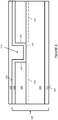
- the gate trench 112 may be formed by an anisotropic plasma etching process that is selective between the different materials of the buffer and barrier regions 106, 108 (e.g., GaN and AIGaN). The gate trench 112 etching process is controlled to stop at or near the interface between the buffer and barrier regions 106, 108.
- the process can be controlled to completely etch through the barrier region 108 and to etch a small depth into the buffer region 106.
- a thin (e.g., 1-2 nm thick) etch stop layer (not shown) of AIN or InAIN, for example, may be provided between the buffer and barrier regions 106, 108. This etch stop layer may be used to stop the gate trench 112 etching process once the barrier region 108 is completely removed.
- an isotropic process can be used to form the gate trench such that the outer sidewalls 116 are disposed at an inclined angle relative to the main surface 102 of the heterostructure body 100.
- a second barrier layer 118 is formed.
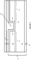
- the second barrier layer 118 lines the bottom 114 and sidewalls of the gate trench 112. Accordingly, the buffer region 106 is covered by the second barrier layer 118.
- the second barrier layer 118 can have the same material composition as the barrier region 108.
- the second barrier layer 118 can be a layer of AIGaN with the same aluminum content as an AIGaN barrier region 108.
- the second barrier layer 118 can have a different aluminum content as an AIGaN barrier region 108.
- the second barrier layer 118 is formed by an epitaxial growth technique. In this way, the second barrier layer 118 conforms to the outer surface of the barrier region 108 in the depicted manner.
- a layer of doped semiconductor material 120 is formed on the second barrier layer 118.
- the layer of doped semiconductor material 120 is formed such that the gate trench 112 is filled by the doped semiconductor material. Due to the presence of the second barrier layer 118 in the gate trench 112, the layer of doped semiconductor material 120 is separated from the buffer region 106 by the second barrier layer 118.
- the layer of doped semiconductor material 120 is formed by an epitaxial growth technique. According to this technique, the layer of doped semiconductor material 120 is epitaxially grown on an exposed outer surface of the barrier region 108 that includes the gate trench 112. The epitaxy process can be carried out such that the layer of doped semiconductor material 120 is sufficiently thick to completely fill the gate trench 112 with doped semiconductor material.
- the material composition of the layer of doped semiconductor material 120 is selected to deplete the section of the two-dimensional charge carrier gas channel 110 that is subjacent to the gate trench 112 at zero external bias. This can be done by selecting a doping concentration for the doped semiconductor material that generates an electric field sufficient to deplete the two-dimensional charge carrier gas channel 110 in a region that is immediately below the gate trench 112. In the example of a GaN/AIGaN heterostructure body 100, this local depletion can be achieved by forming the layer of doped semiconductor material 120 as a layer of p-type GaN.
- an electrically conductive layer 122 is formed on the layer of doped semiconductor material 120.
- the electrically conductive layer 122 can be any electrical conductive metal.
- Exemplary materials for the electrically conductive layer 122 include Ti, TiN, W, TiW and Mo.
- the electrically conductive layer 122 can be formed using a deposition technique, such as a physical vapor deposition (PVD) technique in which the electrically conductive material is deposited directly on the layer of doped semiconductor material 120.
- PVD physical vapor deposition
- a wet chemical surface treatment may be performed to remove any residual oxide on the layer of doped semiconductor material 120.
- a structured mask 124 is formed on the electrically conductive layer 122.
- the structured mask 124 is aligned with the gate trench 112 in such a way that the gate trench 112 is completely covered by the structured mask 124. That is, a center of the structured mask 124 is disposed directly over a center of the gate trench 112, and the structured mask 124 is at least as wide as the gate trench 112.
- the structured mask 124 is wider than the gate trench 112 such that there is at least some lateral overlap of the edges 126 of the structured mask 124 past the outer sidewalls 116 of the trench.
- the structured mask 124 can be formed using a commonly known photolithography technique. More particularly, a photomask can be used to form both the gate trench 112 and the structured mask 124. In this way, the structured mask 124 is self-aligned with the gate trench 112.
- FIG. 7 sections of the layer of doped semiconductor material 120 and the electrically conductive layer 122 that are exposed from the structured mask 124 are removed. According to an embodiment, this is done by a two-step etching process.
- a first step of this two-step etching process is depicted in Fig. 7 .
- the electrically conductive material of the electrically conductive layer 122 is etched selective to the doped semiconductor material of the layer of doped semiconductor material 120. This can be done using a fluorine based plasma treatment, for example.
- a second step of this two-step etching process is depicted in Fig. 8 .
- the material of the layer of doped semiconductor material 120 is etched selective to the material of the barrier region 108. This can be done using a using a chlorine based plasma treatment that additionally includes oxygen or fluorine, for example.
- the above described structuring techniques provide a gate structure 126 that includes a narrower portion 128 of the doped semiconductor material that is disposed in the gate trench 112, a wider portion 130 of the doped semiconductor material that is above the gate trench 112, and laterally extends past outer sidewalls 116 of the gate trench 112, and a gate electrode portion 132 that is formed by electrically conductive material.
- the gate electrode portion 132 completely covers the wider portion 130 of the doped semiconductor material. That is, the gate electrode portion 132 extends along an entire upper surface of the doped semiconductor material.
- the structured mask 124 is removed. This may be done by commonly known photoresist stripping techniques. Subsequently, a wet chemical cleaning process can be performed to remove any residual oxide. Subsequently, electrically conductive source and drain electrodes 134, 136 are formed on the heterostructure body 100.
- the source and drain electrodes 134, 136 can be formed from any of a variety of electrically conductive metals, such as Ti, TiN, W, TiW and Mo, for example.
- the source and drain electrodes 134, 136 ohmically contact the two-dimensional charge carrier gas channel 110.
- the source and drain electrodes 134, 136 extend completely through the barrier region 108 and physically contact the two-dimensional charge carrier gas channel 110.
- physical contact is not necessary and the source and drain electrodes 134, 136 may alternatively be spaced apart from the two-dimensional charge carrier gas channel 110 but nonetheless be in ohmic connection with the channel of the device.
- the source and drain electrodes 134, 136 can be formed by can be formed by a deposition technique, such as a physical vapor deposition (PVD) technique.
- PVD physical vapor deposition
- a passivation layer 138 is formed on the heterostructure body 100.
- the passivation layer 138 can include any material that electrically insulates and protects the surface of the heterostructure body 100. Examples of these materials include semiconductor nitrides, semiconductor oxides, and semiconductor oxynitrides such as silicon nitride (SiN), silicon dioxide (SiO 2 ), and silicon oxynitride (SiO x N y ).
- the passivation layer 138 can be formed by a deposition technique such as a plasma enhanced chemical vapor deposition (PECVD) technique.
- PECVD plasma enhanced chemical vapor deposition
- the passivation layer 138 can be formed on a portion of the semiconductor device that includes the gate structure 126 such that the passivation layer 138 completely covers the gate electrode portion 132.
- the passivation layer 138 extends over an entire upper surface of the gate electrode portion 132. Electrical contact to the gate electrode portion 132 (e.g., via conductive plugs) can be effectuated in other cross-sectional regions (not shown).
- an upper surface 140 of the passivation layer 138 is planarized. This may be done by a chemical-mechanical planarization (CMP) technique, for example. As a result, the upper surface 140 of the semiconductor device extends along a single plane. Moreover, this plane is parallel to the main and rear surfaces 102, 104 of the heterostructure body 100.
- CMP chemical-mechanical planarization
- the gate structure 126 is configured to control a conductive state of two-dimensional charge carrier gas channel 110. ON/OFF control is achieved by suitable biasing of the gate electrode portion 132. The presence of the doped semiconductor material in the gate structure 126 modifies the intrinsically conductive state of the two-dimensional charge carrier gas channel 110 such that a conductive connection between the source and drain electrodes 134, 136 does not exist when gate electrode portion 132 is unbiased.
- the gate structure 126 is configured to turn the device ON with a sufficient voltage (V TH ) applied to the gate electrode that removes the depleted region of the two-dimensional charge carrier gas underneath the gate structure 126. As a result, the two-dimensional charge carrier gas channel 110 forms a conductive connection between the source and drain electrodes 134, 136.
- Figs. 10 , 11 and 12 depict selected method steps for forming the semiconductor device, according to another embodiment. Those method steps that are not discussed with reference to Figs. 10 , 11 and 12 may be substantially similar or identical the previous method steps described with reference to Figs. 1-9 .
- a heterostructure body 100 is provided and a gate trench 112 is formed in the heterostructure body 100.
- the heterostructure body 100 may be provided according to the technique described with reference to Fig. 1 .
- a section of the barrier region 108 is only partially removed to form the gate trench 112.
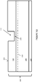
- a portion 138 of the barrier region 108 remains between a bottom 114 of the gate trench 112 and the barrier region 108. That is, the gate trench 112 formation process does not expose the buffer region 106.
- the barrier region 108 is completely removed in a lateral section to expose the buffer region 106 at the bottom 114 of the gate trench 112.
- the gate trench 112 is formed by a time-controlled anisotropic plasma-etching process that is controlled to stop etching before reaching the buffer region 106. This process can be controlled such that the thickness of the remaining portion of the barrier region 108 at the bottom 114 of the gate trench 112 is approximately 5 to 20 nanometers (nm) thick, for example.
- a layer of doped semiconductor material 120 and an electrically conductive layer 122 are formed on the heterostructure body 100.
- the layer of doped semiconductor material 120 and the electrically conductive layer 122 can each be formed according to the techniques described with reference to Figs. 4 and 5 , respectively, and can each have the material composition of these layers as previously described. Different to the previous embodiment, the layer of doped semiconductor material 120 is formed directly on the surface of the buffer region 106.
- source and drain electrodes 134, 136 and the passivation layer 138 are formed. These features may be formed according to the techniques described with reference to Fig. 9 . As a result, a semiconductor device that is configured to control the conductive state of the two-dimensional charge carrier gas channel 110. Different to the embodiment of Fig, 9 , there is no second barrier layer 118 interposed between the layer of doped semiconductor material 120 and the buffer region 106.
- the gate structure 126 of the device described herein is formed by a self-aligned patterning technique wherein the doped semiconductor material and the gate electrode are structured using a common photomask, a minimal L td (lateral extension towards the drain) of the gate structure 126 can be achieved.
- the L td is measured between an outer sidewall 116 of the gate trench 112 that is closest to the drain electrode 136 and an outer edge of the doped semiconductor material in the wider portion 130.
- the present techniques can include a self-aligned technique whereby a common photomask is used to form the gate trench 112 and the structured mask 124 that is used to form the gate structure 126, L td values of 100 nm or less can be achieved.
- an overlapping gate structure 126 for an HEMT device is formed by a process that includes filling the trench with a doped semiconductor layer, subsequently structuring the doped semiconductor layer, subsequently depositing a passivation layer, subsequently etching a trench in the passivation layer, and subsequently depositing a gate metal in the trench of the passivation layer. That is, in the conventional technique, the gate metal is formed after structuring the doped semiconductor layer and forming the passivation layer. Due to the processing tolerances of this technique, a margin between the edge of the gate via and the edge of the doped semiconductor region is required. As a result, an L td value of 300 nm impossible to achieve with this technique.
- C GD gate-drain capacitance
- An additional benefit to the electrical characteristics is achieved by the above described techniques by forming the gate structure 126 without exposing the bottom 114 of the gate trench 112 to damaging etchant (e.g., plasma etchant).
- etchant e.g., plasma etchant
- a plasma etch is performed after filling the gate trench 112 with doped semiconductor material.
- the doped semiconductor material is etched in such a way that the etchant reaches the bottom 114 of the gate trench 112. This results in damage to the semiconductor material at the bottom 114 of the gate trench 112.
- current collapse, dynamic R DSON , and threshold voltage shift under pulsed conditions are expected to be significantly reduced.
- the above described technique produces a device with advantageous physical characteristics. Because the doped semiconductor and the gate conductor are first structured and the passivation layer 138 is subsequently deposited, the outer surface of the passivation layer 138 corresponds to the uppermost surface of the device.
- the passivation layer 138 can be planarized to form a device with a low vertical profile, and an upper surface that extends along a single plane.
- the vertical profile of the device is increased and the uppermost surface of the device is multi-tiered.
- the resultant structure includes gate metal protruding out of the passivation layer 138 and planarization is therefore not possible.
- the device described herein has a simplified structure that is easier to incorporate into a semiconductor package.
- the above described techniques have reduced process complexity and expense in comparison to conventional techniques.
- the presently described technique forms the gate structure 126 using a self-aligned technique in which the gate trench 112 and the structured mask 124 are formed using a common photomask.
- the structured mask 124 is used to etch both the doped semiconductor material and the gate conductor.
- conventional techniques typically include separate masking and etching steps for structuring both the doped semiconductor material portion and the electrode portion of the gate electrode.
- HEMT is also commonly referred to as HFET (heterostructure field effect transistor), MODFET (modulation-doped FET) and MESFET (metal semiconductor field effect transistor).
- HFET heterostructure field effect transistor
- MODFET modulation-doped FET
- MESFET metal semiconductor field effect transistor
- III-nitride based compound semiconductor transistor incorporating a junction between two materials with different band gaps (i.e., a heterojunction) as the channel.
- GaN may be combined with AIGaN or InGaN to form an electron gas inversion region as the channel.
- the compound semiconductor device may have AlInN/AlN/GaN barrier/spacer/buffer layer structures.
- the normally-off compound semiconductor transistor can be realized using any suitable III-nitride technology such as GaN that permits the formation of opposite polarity inversion regions due to piezoelectric effects.
- the presence of polarization charges and strain effects in a GaN-based heterostructure body due to piezoelectric effects yield a two-dimensional charge carrier gas in the heterostructure body characterized by very high carrier density and carrier mobility.
- a two-dimensional charge carrier gas such as a 2DEG (two-dimensional electron gas) or 2DHG (two-dimensional hole gas)
- a thin, e.g. 1-2nm, AIN layer can be provided between the GaN buffer region and the GaN alloy barrier region to minimize alloy scattering and enhance 2DEG mobility.
- the compound semiconductor transistors described herein can be formed from any binary, ternary or quaternary III-nitride compound semiconductor material where piezoelectric effects are responsible for the device concept.
- doping regions of the same relative doping concentration do not necessarily have the same absolute doping concentration.
- two different "n"-doping regions may have the same or different absolute doping concentrations.
- the doped portions are designated as being "p" or "n"-doped. As is clearly to be understood, this designation is by no means intended to be limiting.
- the doping type can be arbitrary as long as the described functionality is achieved. Further, in all embodiments, the doping types can be reversed.
Landscapes
- Insulated Gate Type Field-Effect Transistor (AREA)
- Engineering & Computer Science (AREA)
- Manufacturing & Machinery (AREA)
- Junction Field-Effect Transistors (AREA)
- Electrodes Of Semiconductors (AREA)
Abstract
Description
- The instant application generally relates to high electron mobility transistors, and more particularly relates to the formation of gate structures for normally-off high electron mobility transistors.
- Semiconductor transistors, in particular field-effect controlled switching devices such as a MISFET (Metal Insulator Semiconductor Field Effect Transistor), in the following also referred to as MOSFET (Metal Oxide Semiconductor Field Effect Transistor) and a HEMT (high-electron-mobility Field Effect Transistor) also known as heterostructure FET (HFET) and modulation-doped FET (MODFET) are used in a variety of applications. An HEMT is a transistor with a junction between two materials having different band gaps, such as GaN and AIGaN. In a GaN/AIGaN based HEMT, a two-dimensional electron gas (2DEG) arises near the interface between the AIGaN barrier layer and the GaN buffer layer. In an HEMT, the 2DEG forms the channel of the device. Similar principles may be utilized to select buffer and barrier layers that form a two-dimensional hole gas (2DHG) as the channel of the device. A 2DEG or a 2DHG is generally referred to as a two-dimensional carrier gas. Without further measures, the heterojunction configuration leads to a self-conducting, i.e., normally-on, transistor. Measures must be taken to prevent the channel region of an HEMT from being in a conductive state in the absence of a positive gate voltage.
- Due to the high electron mobility of the two-dimensional carrier gas in the heterojunction configuration, HEMTs offer high conduction and low losses in comparison to many conventional semiconductor transistor designs. These advantageous conduction characteristics make HEMTs desirable in applications including, but not limited to, use as switches in power supplies and power converters, electric cars, air-conditioners, and in consumer electronics, for example. However, normally-on HEMTs have limited applicability in these applications because these devices must be accompanied by circuitry that can generate the negative voltages necessary to turn the device off. Such circuitry adds cost and complexity to the design. Moreover, for safety reasons, it is typically desirable to have a device that is non-conducting in the absence of a gate bias. For this reason, it is typically desirable to include features in an HEMT that modify the intrinsic normally-on configuration and provide a device with a normally-off configuration (i.e., a positive threshold voltage).
- One technique for providing a normally-off HEMT involves configuring the gate structure to modify the intrinsic conductive state of the 2DEG. For example, a relatively thick (typically 100 nm or greater) p-type doped GaN material can be formed under the gate electrode. This thick p-type GaN layer depletes the inversion layer under the gate structure, shifting the threshold voltage of the device to positive values. The p-type GaN layer must be thick enough to create a vertical field which depletes and populates the naturally occurring inversion channel underlying the barrier layer, typically a layer of AIGaN. The vertical field generated by a voltage applied to the gate electrode allows for on and off modulation of the inversion layer.
- Market competitive devices for high voltage and low voltage applications should ideally provide, among other things, normally-off behavior with a VTH (threshold voltage) of about 1 V (volt), low RDSON (drain-source on-resistance), very low current-collapse, very low dynamic RDSON, very low threshold voltage shift, and low parasitic capacitances. The figure of merit (FOM), which is a device parameter that relates RDSON to QGD (gate charge), is one important parameter that designers seek to improve in furtherance of these goals.
- A method of forming a semiconductor device is provided. According to an embodiment, the method includes providing a heterostructure body with a buffer region, and a barrier region disposed on the buffer region. The barrier region has a different band gap than the buffer region such that a two-dimensional charge carrier gas channel arises near an interface between the buffer region and the barrier region. A gate trench is formed in the barrier region. A layer of doped semiconductor material that fills the gate trench is formed. The doped semiconductor material in the gate trench locally depletes a subjacent section of the two-dimensional charge carrier gas channel at zero bias. A layer of electrically conductive material is formed on the doped semiconductor material. The layer of doped semiconductor material is structured to form a gate structure that is configured to control a conductive state of the two-dimensional charge carrier gas channel. The gate structure includes a narrower portion of the doped semiconductor material that is disposed in the gate trench, a wider portion of the doped semiconductor material that is above the gate trench and laterally extends past outer sidewalls of the gate trench, and a gate electrode portion of the electrically conductive material that completely covers the wider portion of the doped semiconductor material.
- Forming the layer of doped semiconductor material may comprise epitaxially growing the layer of doped semiconductor material on an exposed outer surface of the barrier region that includes the gate trench, and wherein forming the layer of electrically conductive material comprises depositing the electrically conductive material directly on the layer of doped semiconductor material.
- Structuring the layer of doped semiconductor material may comprise forming a structured mask on the layer of electrically conductive material, the structured mask being disposed directly above the gate trench and being wider than the gate trench; and removing sections of the layer of doped semiconductor material and the layer of electrically conductive material that are exposed from the structured mask.
- Removing the sections of the layer of doped semiconductor material and the layer of electrically conductive material may comprise a two-step etching process, the two-step etching process comprising etching the electrically conductive material selective to the doped semiconductor material; and subsequently etching the doped semiconductor material selective to material of the barrier region.
- In some embodiments, the method further comprises removing the structured mask after removing the sections of the layer of doped semiconductor material and the layer of electrically conductive material; and forming an electrically insulating passivation layer on the heterostructure body after removing the structured mask.
- Forming the electrically insulating passivation layer may comprise depositing the electrically insulating passivation layer on a portion of the semiconductor device that includes the gate structure such that the passivation layer completely covers the gate electrode portion.
- In some embodiments, forming the gate trench comprises etching a section of the barrier region completely away such that the buffer region is exposed at a bottom of the gate trench, and the method further comprises forming a second barrier layer that lines the bottom and sidewalls of the gate trench: and forming the layer of doped semiconductor material on the second barrier layer such that the doped semiconductor material is separated from the buffer region by the second barrier layer.
- In some embodiments, forming the gate trench comprises etching a section of the barrier region partially away such that a portion of the barrier region remains between a bottom of the gate trench and the barrier region, and the method further comprises forming the layer of doped semiconductor material directly on the sidewalls and bottom of the gate trench.
- In some embodiments, the method further comprises forming electrically conductive source and drain electrodes on the heterostructure body, each of the source and drain electrodes being in ohmic contact with the two dimensional charge carrier gas channel, wherein the wider portion of the doped semiconductor material laterally extends past an outer sidewall of the gate trench that is closest to the drain electrode by no more than 100 µm.
- According to another embodiment, the method includes providing a heterostructure body with a buffer region, and a barrier region disposed on the buffer region. The barrier region has a different band gap than the buffer region such that a two-dimensional charge carrier gas channel arises near an interface between the buffer region and the barrier region. A gate trench is formed in the barrier region. A layer of doped semiconductor material that fills the gate trench is formed. The doped semiconductor material in the gate trench locally depletes a subjacent section of the two-dimensional charge carrier gas channel at zero bias. A layer of electrically conductive material is formed on the doped semiconductor material. The layer of doped semiconductor material is structured to form a gate structure that is configured to control a conductive state of the two-dimensional charge carrier gas channel. An electrically insulating passivation layer is formed on the barrier region and the gate structure after structuring the layer of doped semiconductor material and the layer of electrically conductive material.
- In an embodiment, forming the layer of doped semiconductor material comprises epitaxially growing the layer of doped semiconductor material on an exposed outer surface of the barrier region that includes the gate trench, and wherein forming the layer of electrically conductive material comprises depositing the electrically conductive material directly on the layer of doped semiconductor material.
- In an embodiment, structuring the layer of doped semiconductor material comprises forming a structured mask on the layer of electrically conductive material, the structured mask being disposed directly above the gate trench and being wider than the gate trench; and removing sections of the layer of doped semiconductor material and the layer of electrically conductive material that are exposed from the structured mask such that the gate structure comprises a wider portion of the doped semiconductor material that is above the gate trench and laterally extends past outer sidewalls of the gate trench; and a gate electrode portion of the electrically conductive material that completely covers the wider portion of the doped semiconductor material.
- In an embodiment, removing the sections of the layer of doped semiconductor material and the layer of electrically conductive material comprises a two-step etching process, the two-step etching process comprising etching the electrically conductive material selective to the doped semiconductor material; and subsequently etching the doped semiconductor material selective to material of the barrier region.
- In some embodiments, forming the electrically insulating passivation layer comprises depositing the electrically insulating passivation layer on a portion of the semiconductor device that includes the gate structure such that the passivation layer completely covers the gate electrode portion.
- In some embodiments, the method further comprises forming electrically conductive source and drain electrodes on the heterostructure body, each of the source and drain electrodes being in ohmic contact with the two dimensional charge carrier gas channel, wherein the wider portion of the of the doped semiconductor material laterally extends past an outer sidewall of the gate trench that is closest to the drain electrode by no more than 100 µm.
- In some embodiments, forming the gate trench comprises etching a section of the barrier region completely away such that the buffer region is exposed at a bottom of the gate trench, the method further comprising forming a second barrier layer that lines the bottom and sidewalls of the gate trench; and forming the layer of doped semiconductor material on the second barrier layer such that the doped semiconductor material is separated from the buffer region by the second barrier layer.
- In some embodiments, forming the gate trench comprises etching a section of the barrier region partially away such that a portion of the barrier region remains between a bottom of the gate trench and the barrier region, the method further comprising forming the layer of doped semiconductor material directly on the sidewalls and bottom of the gate trench.
- A semiconductor device is disclosed. According to an embodiment, the semiconductor device includes a heterostructure body with a buffer region, and a barrier region disposed on the buffer region. The barrier region has a different band gap than the buffer region such that a two-dimensional charge carrier gas channel arises near an interface between the buffer region and the barrier region. A gate trench is formed in the barrier region. A gate structure is configured to control a conductive state of the two-dimensional charge carrier gas channel. The gate structure includes a narrower portion of doped semiconductor material that is disposed in the gate trench, a wider portion of doped semiconductor material that is above the gate trench and laterally extends past outer sidewalls of the gate trench, and a gate electrode portion of electrically conductive material that completely covers the wider portion of the doped semiconductor material. The doped semiconductor material is configured to locally deplete the two-dimensional charge carrier gas channel at zero bias.
- The semiconductor device may further comprise electrically conductive source and drain electrodes on the heterostructure body, each of the source and drain electrodes being in ohmic contact with the two dimensional charge carrier gas channel; and an electrically insulating passivation layer that completely covers the source and drain electrodes, the gate structure, and an outer surface of the barrier region between the source and drain electrodes and the gate structure, wherein an upper surface of the passivation layer is planarized.
- In some embodiments, the wider portion of the doped semiconductor material laterally extends past an outer sidewall of the gate trench that is closest to the drain electrode by no more than 100 µm.
- The elements of the drawings are not necessarily to scale relative to each other. Like reference numerals designate corresponding similar parts. The features of the various illustrated embodiments can be combined unless they exclude each other. Embodiments are depicted in the drawings and are detailed in the description which follows.
-
Figure 1 illustrates a heterostructure body, according to an embodiment. -
Figure 2 illustrates forming a gate trench in the heterostructure body, according to an embodiment. -
Figure 3 illustrates orming a barrier layer on the heterostructure body, according to an embodiment. -
Figure 4 illustrates forming a doped semiconductor layer that fills the gate trench, according to an embodiment. -
Figure 5 illustrates forming an electrically conductive layer on the doped semiconductor layer, according to an embodiment. -
Figure 6 illustrates forming structured mask on the electrically conductive layer, according to an embodiment. -
Figure 7 illustrates removing exposed sections of the electrically conductive layer, according to an embodiment. -
Figure 8 illustrates removing exposed sections of the doped semiconductor layer, according to an embodiment. -
Figure 9 illustrates forming source and drain electrodes and a passivation layer on the heterostructure body, according to an embodiment. -
Figure 10 illustrates forming a gate trench in the heterostructure body, according to another embodiment. -
Figure 11 illustrates forming a doped semiconductor layer and an electrically conductive layer on the heterostructure body ofFig. 10 , according to another embodiment. -
Figure 12 illustrates forming source and drain electrodes and a passivation layer on the heterostructure body ofFig. 11 , according to an embodiment. - Embodiments described herein include forming a gate structure for normally-off HEMT device with a self-aligned technique. According to this technique, a heterostructure body with a barrier and buffer region is provided. A gate trench is formed in the barrier region of the semiconductor body, e.g., by anisotropic etching. The gate trench is filled with a layer of doped semiconductor material (e.g., p-type GaN) that is configured to locally deplete the two-dimensional charge carrier gas channel. An electrically conductive layer (e.g., aluminum) is then deposited on the doped semiconductor layer. A structured mask is formed on the electrically conductive layer and used to structure both the electrically conductive layer and the layer of doped semiconductor material. This structuring produces a gate structure that fills the gate trench and includes a wider portion above the gate trench that slightly overlaps past the sidewalls of the trench. Subsequently, an electrically insulating passivation layer (SiN) is formed on the heterostructure body and over the gate structure. This technique produces a normally-off HEMT device with improved FOM (figure of merit) in comparison to prior art devices, due to a reduced Ltd (lateral extension towards the drain) of the gate structure, and improved current collapse, dynamic RDSON, and threshold voltage shift, due to reduced surface damage in the gate region in comparison to prior art devices.
- Referring to
Fig. 1 , aheterostructure body 100 is provided. Theheterostructure body 100 includes amain surface 102 and arear surface 104 opposite themain surface 102. Theheterostructure body 100 includes abuffer region 106 and abarrier region 108 disposed on thebuffer region 106. The material of thebarrier region 108 has a different bandgap as the material of thebuffer region 106 such that a two-dimensional chargecarrier gas channel 110 arises near an interface between thebuffer region 106 and thebarrier region 108. According to an embodiment, thebuffer region 106 is a region of GaN (gallium nitride) and thebarrier region 108 is a region of AIGaN (aluminum gallium nitride). In that case, the two-dimensional chargecarrier gas channel 110 is a 2DEG (two-dimensional charge carrier gas channel). - According to an embodiment, the
buffer region 106 and thebarrier region 108 of theheterostructure body 100 are epitaxial layers that are formed according to epitaxial growth techniques. According to this process, abase substrate 110 is provided. Thebase substrate 110 can include any material that is suitable for epitaxial growth thereon. Exemplary materials for thebase substrate 110 include silicon and carbon. Thebase substrate 110 can be provided from a bulk semiconductor substrate or alternatively can be formed using an epitaxy process. After providing thebase substrate 110, thebuffer region 106 is epitaxially grown on the base region, and thebarrier region 108 is epitaxially grown on thebuffer region 106. A lattice transition layer (not shown) may be provided between thebase substrate 110 and thebuffer region 106 to reduce lattice mismatch between the two regions. - Referring to
Fig. 2 , agate trench 112 is formed in theheterostructure body 100. According to an embodiment, thegate trench 112 is formed by etching a section of thebarrier region 108 completely away such that thebuffer region 106 is exposed at a bottom 114 of thegate trench 112. That is, an entire thickness of thebarrier region 108 is removed in a lateral section of thebarrier region 108. Thegate trench 112 may be formed by an anisotropic plasma etching process that is selective between the different materials of the buffer andbarrier regions 106, 108 (e.g., GaN and AIGaN). Thegate trench 112 etching process is controlled to stop at or near the interface between the buffer andbarrier regions barrier region 108 and to etch a small depth into thebuffer region 106. According to another option, a thin (e.g., 1-2 nm thick) etch stop layer (not shown) of AIN or InAIN, for example, may be provided between the buffer andbarrier regions gate trench 112 etching process once thebarrier region 108 is completely removed. Instead of an anisotropic process, an isotropic process can be used to form the gate trench such that theouter sidewalls 116 are disposed at an inclined angle relative to themain surface 102 of theheterostructure body 100. - Referring to
Fig. 3 , asecond barrier layer 118 is formed. Thesecond barrier layer 118 lines the bottom 114 and sidewalls of thegate trench 112. Accordingly, thebuffer region 106 is covered by thesecond barrier layer 118. Thesecond barrier layer 118 can have the same material composition as thebarrier region 108. For example, thesecond barrier layer 118 can be a layer of AIGaN with the same aluminum content as anAIGaN barrier region 108. Alternatively, thesecond barrier layer 118 can have a different aluminum content as anAIGaN barrier region 108. According to an embodiment, thesecond barrier layer 118 is formed by an epitaxial growth technique. In this way, thesecond barrier layer 118 conforms to the outer surface of thebarrier region 108 in the depicted manner. - Referring to
Fig. 4 , a layer of dopedsemiconductor material 120 is formed on thesecond barrier layer 118. The layer of dopedsemiconductor material 120 is formed such that thegate trench 112 is filled by the doped semiconductor material. Due to the presence of thesecond barrier layer 118 in thegate trench 112, the layer of dopedsemiconductor material 120 is separated from thebuffer region 106 by thesecond barrier layer 118. According to an embodiment, the layer of dopedsemiconductor material 120 is formed by an epitaxial growth technique. According to this technique, the layer of dopedsemiconductor material 120 is epitaxially grown on an exposed outer surface of thebarrier region 108 that includes thegate trench 112. The epitaxy process can be carried out such that the layer of dopedsemiconductor material 120 is sufficiently thick to completely fill thegate trench 112 with doped semiconductor material. - The material composition of the layer of doped
semiconductor material 120 is selected to deplete the section of the two-dimensional chargecarrier gas channel 110 that is subjacent to thegate trench 112 at zero external bias. This can be done by selecting a doping concentration for the doped semiconductor material that generates an electric field sufficient to deplete the two-dimensional chargecarrier gas channel 110 in a region that is immediately below thegate trench 112. In the example of a GaN/AIGaN heterostructure body 100, this local depletion can be achieved by forming the layer of dopedsemiconductor material 120 as a layer of p-type GaN. - Referring to
Fig. 5 , an electricallyconductive layer 122 is formed on the layer of dopedsemiconductor material 120. Generally speaking, the electricallyconductive layer 122 can be any electrical conductive metal. Exemplary materials for the electricallyconductive layer 122 include Ti, TiN, W, TiW and Mo. The electricallyconductive layer 122 can be formed using a deposition technique, such as a physical vapor deposition (PVD) technique in which the electrically conductive material is deposited directly on the layer of dopedsemiconductor material 120. Optionally, prior to the deposition of the electricallyconductive layer 122, a wet chemical surface treatment may be performed to remove any residual oxide on the layer of dopedsemiconductor material 120. - Referring to
Fig. 6 , astructured mask 124 is formed on the electricallyconductive layer 122. Thestructured mask 124 is aligned with thegate trench 112 in such a way that thegate trench 112 is completely covered by the structuredmask 124. That is, a center of the structuredmask 124 is disposed directly over a center of thegate trench 112, and thestructured mask 124 is at least as wide as thegate trench 112. According to an embodiment, thestructured mask 124 is wider than thegate trench 112 such that there is at least some lateral overlap of theedges 126 of the structuredmask 124 past theouter sidewalls 116 of the trench. Thestructured mask 124 can be formed using a commonly known photolithography technique. More particularly, a photomask can be used to form both thegate trench 112 and thestructured mask 124. In this way, thestructured mask 124 is self-aligned with thegate trench 112. - Referring to
Figs. 7 and8 , sections of the layer of dopedsemiconductor material 120 and the electricallyconductive layer 122 that are exposed from the structuredmask 124 are removed. According to an embodiment, this is done by a two-step etching process. A first step of this two-step etching process is depicted inFig. 7 . In this step, the electrically conductive material of the electricallyconductive layer 122 is etched selective to the doped semiconductor material of the layer of dopedsemiconductor material 120. This can be done using a fluorine based plasma treatment, for example. A second step of this two-step etching process is depicted inFig. 8 . In this step, the material of the layer of dopedsemiconductor material 120 is etched selective to the material of thebarrier region 108. This can be done using a using a chlorine based plasma treatment that additionally includes oxygen or fluorine, for example. - The above described structuring techniques provide a
gate structure 126 that includes anarrower portion 128 of the doped semiconductor material that is disposed in thegate trench 112, awider portion 130 of the doped semiconductor material that is above thegate trench 112, and laterally extends pastouter sidewalls 116 of thegate trench 112, and agate electrode portion 132 that is formed by electrically conductive material. Thegate electrode portion 132 completely covers thewider portion 130 of the doped semiconductor material. That is, thegate electrode portion 132 extends along an entire upper surface of the doped semiconductor material. - Referring to
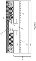
Fig. 9 , further processing steps are performed. First, thestructured mask 124 is removed. This may be done by commonly known photoresist stripping techniques. Subsequently, a wet chemical cleaning process can be performed to remove any residual oxide. Subsequently, electrically conductive source and drainelectrodes heterostructure body 100. The source and drainelectrodes electrodes carrier gas channel 110. According to one embodiment, the source and drainelectrodes barrier region 108 and physically contact the two-dimensional chargecarrier gas channel 110. However, physical contact is not necessary and the source and drainelectrodes carrier gas channel 110 but nonetheless be in ohmic connection with the channel of the device. The source and drainelectrodes - A
passivation layer 138 is formed on theheterostructure body 100. Generally speaking, thepassivation layer 138 can include any material that electrically insulates and protects the surface of theheterostructure body 100. Examples of these materials include semiconductor nitrides, semiconductor oxides, and semiconductor oxynitrides such as silicon nitride (SiN), silicon dioxide (SiO2), and silicon oxynitride (SiOxNy). Thepassivation layer 138 can be formed by a deposition technique such as a plasma enhanced chemical vapor deposition (PECVD) technique. Thepassivation layer 138 can be formed on a portion of the semiconductor device that includes thegate structure 126 such that thepassivation layer 138 completely covers thegate electrode portion 132. That is, from the cross-sectional perspective ofFig. 9 , thepassivation layer 138 extends over an entire upper surface of thegate electrode portion 132. Electrical contact to the gate electrode portion 132 (e.g., via conductive plugs) can be effectuated in other cross-sectional regions (not shown). - According to an embodiment, after the
passivation layer 138 is formed, anupper surface 140 of thepassivation layer 138 is planarized. This may be done by a chemical-mechanical planarization (CMP) technique, for example. As a result, theupper surface 140 of the semiconductor device extends along a single plane. Moreover, this plane is parallel to the main andrear surfaces heterostructure body 100. - In a commonly known manner, the
gate structure 126 is configured to control a conductive state of two-dimensional chargecarrier gas channel 110. ON/OFF control is achieved by suitable biasing of thegate electrode portion 132. The presence of the doped semiconductor material in thegate structure 126 modifies the intrinsically conductive state of the two-dimensional chargecarrier gas channel 110 such that a conductive connection between the source and drainelectrodes gate electrode portion 132 is unbiased. Thegate structure 126 is configured to turn the device ON with a sufficient voltage (VTH) applied to the gate electrode that removes the depleted region of the two-dimensional charge carrier gas underneath thegate structure 126. As a result, the two-dimensional chargecarrier gas channel 110 forms a conductive connection between the source and drainelectrodes -
Figs. 10 ,11 and12 depict selected method steps for forming the semiconductor device, according to another embodiment. Those method steps that are not discussed with reference toFigs. 10 ,11 and12 may be substantially similar or identical the previous method steps described with reference toFigs. 1-9 . - Referring to
Fig. 10 , aheterostructure body 100 is provided and agate trench 112 is formed in theheterostructure body 100. Theheterostructure body 100 may be provided according to the technique described with reference toFig. 1 . Subsequently, a section of thebarrier region 108 is only partially removed to form thegate trench 112. As a result, aportion 138 of thebarrier region 108 remains between a bottom 114 of thegate trench 112 and thebarrier region 108. That is, thegate trench 112 formation process does not expose thebuffer region 106. This is different to the technique described with reference toFig. 2 in which thebarrier region 108 is completely removed in a lateral section to expose thebuffer region 106 at the bottom 114 of thegate trench 112. According to an embodiment, thegate trench 112 is formed by a time-controlled anisotropic plasma-etching process that is controlled to stop etching before reaching thebuffer region 106. This process can be controlled such that the thickness of the remaining portion of thebarrier region 108 at the bottom 114 of thegate trench 112 is approximately 5 to 20 nanometers (nm) thick, for example. - Referring to
Fig. 11 , a layer of dopedsemiconductor material 120 and an electricallyconductive layer 122 are formed on theheterostructure body 100. The layer of dopedsemiconductor material 120 and the electricallyconductive layer 122 can each be formed according to the techniques described with reference toFigs. 4 and5 , respectively, and can each have the material composition of these layers as previously described. Different to the previous embodiment, the layer of dopedsemiconductor material 120 is formed directly on the surface of thebuffer region 106. - Referring to
Fig. 12 , source and drainelectrodes passivation layer 138 are formed. These features may be formed according to the techniques described with reference toFig. 9 . As a result, a semiconductor device that is configured to control the conductive state of the two-dimensional chargecarrier gas channel 110. Different to the embodiment ofFig, 9 , there is nosecond barrier layer 118 interposed between the layer of dopedsemiconductor material 120 and thebuffer region 106. - The above described techniques produce a device with advantageous electrical characteristics. Because the
gate structure 126 of the device described herein is formed by a self-aligned patterning technique wherein the doped semiconductor material and the gate electrode are structured using a common photomask, a minimal Ltd (lateral extension towards the drain) of thegate structure 126 can be achieved. The Ltd is measured between anouter sidewall 116 of thegate trench 112 that is closest to thedrain electrode 136 and an outer edge of the doped semiconductor material in thewider portion 130. Because the present techniques can include a self-aligned technique whereby a common photomask is used to form thegate trench 112 and thestructured mask 124 that is used to form thegate structure 126, Ltd values of 100 nm or less can be achieved. By contrast, in a conventional technique, an overlappinggate structure 126 for an HEMT device is formed by a process that includes filling the trench with a doped semiconductor layer, subsequently structuring the doped semiconductor layer, subsequently depositing a passivation layer, subsequently etching a trench in the passivation layer, and subsequently depositing a gate metal in the trench of the passivation layer. That is, in the conventional technique, the gate metal is formed after structuring the doped semiconductor layer and forming the passivation layer. Due to the processing tolerances of this technique, a margin between the edge of the gate via and the edge of the doped semiconductor region is required. As a result, an Ltd value of 300 nm impossible to achieve with this technique. By substantially reducing the Ltd value using the presently disclosed techniques, CGD (gate-drain capacitance) is correspondingly reduced. Consequently, a dramatic improvement in parasitic capacitance, an improved figure of merit (FOM), lower RDSON and reduced switching losses are achieved in comparison to the conventionally formed device. - An additional benefit to the electrical characteristics is achieved by the above described techniques by forming the
gate structure 126 without exposing thebottom 114 of thegate trench 112 to damaging etchant (e.g., plasma etchant). According a conventional technique, a plasma etch is performed after filling thegate trench 112 with doped semiconductor material. The doped semiconductor material is etched in such a way that the etchant reaches the bottom 114 of thegate trench 112. This results in damage to the semiconductor material at the bottom 114 of thegate trench 112. By eliminating this surface damage using the presently disclosed techniques, current collapse, dynamic RDSON, and threshold voltage shift under pulsed conditions are expected to be significantly reduced. - In addition, the above described technique produces a device with advantageous physical characteristics. Because the doped semiconductor and the gate conductor are first structured and the
passivation layer 138 is subsequently deposited, the outer surface of thepassivation layer 138 corresponds to the uppermost surface of the device. Thepassivation layer 138 can be planarized to form a device with a low vertical profile, and an upper surface that extends along a single plane. By way of comparison, in a conventional device that is formed by structuring the doped semiconductor, subsequently depositing apassivation layer 138, etching a trench in thepassivation layer 138, and depositing a gate metal in the trench of thepassivation layer 138, the vertical profile of the device is increased and the uppermost surface of the device is multi-tiered. The resultant structure includes gate metal protruding out of thepassivation layer 138 and planarization is therefore not possible. Thus, the device described herein has a simplified structure that is easier to incorporate into a semiconductor package. - In addition, the above described techniques have reduced process complexity and expense in comparison to conventional techniques. For example, the presently described technique forms the
gate structure 126 using a self-aligned technique in which thegate trench 112 and thestructured mask 124 are formed using a common photomask. Thestructured mask 124 is used to etch both the doped semiconductor material and the gate conductor. By way of comparison, conventional techniques typically include separate masking and etching steps for structuring both the doped semiconductor material portion and the electrode portion of the gate electrode. - The term HEMT is also commonly referred to as HFET (heterostructure field effect transistor), MODFET (modulation-doped FET) and MESFET (metal semiconductor field effect transistor). The terms HEMT, HFET, MESFET and MODFET are used interchangeably herein to refer to any III-nitride based compound semiconductor transistor incorporating a junction between two materials with different band gaps (i.e., a heterojunction) as the channel. For example, GaN may be combined with AIGaN or InGaN to form an electron gas inversion region as the channel. The compound semiconductor device may have AlInN/AlN/GaN barrier/spacer/buffer layer structures. In general, the normally-off compound semiconductor transistor can be realized using any suitable III-nitride technology such as GaN that permits the formation of opposite polarity inversion regions due to piezoelectric effects.
- Specifically with regard to GaN technology, the presence of polarization charges and strain effects in a GaN-based heterostructure body due to piezoelectric effects yield a two-dimensional charge carrier gas in the heterostructure body characterized by very high carrier density and carrier mobility. Such a two-dimensional charge carrier gas, such as a 2DEG (two-dimensional electron gas) or 2DHG (two-dimensional hole gas), forms the conductive channel of the HEMT near the interface between, e.g., a GaN alloy barrier region and a GaN buffer region. A thin, e.g. 1-2nm, AIN layer can be provided between the GaN buffer region and the GaN alloy barrier region to minimize alloy scattering and enhance 2DEG mobility. In a broad sense, the compound semiconductor transistors described herein can be formed from any binary, ternary or quaternary III-nitride compound semiconductor material where piezoelectric effects are responsible for the device concept.
- In the figures provided herein, doping regions of the same relative doping concentration do not necessarily have the same absolute doping concentration. For example, two different "n"-doping regions may have the same or different absolute doping concentrations. In the Figures and the description, for the sake of a better comprehension, often the doped portions are designated as being "p" or "n"-doped. As is clearly to be understood, this designation is by no means intended to be limiting. The doping type can be arbitrary as long as the described functionality is achieved. Further, in all embodiments, the doping types can be reversed.
- As used herein, the terms "having," "containing," "including," "comprising" and the like are open-ended terms that indicate the presence of stated elements or features, but do not preclude additional elements or features. The articles "a," "an" and "the" are intended to include the plural as well as the singular, unless the context clearly indicates otherwise.
- With the above range of variations and applications in mind, it should be understood that the present invention is not limited by the foregoing description, nor is it limited by the accompanying drawings. Instead, the present invention is limited only by the following claims and their legal equivalents.
Claims (14)
Applications Claiming Priority (1)
| Application Number | Priority Date | Filing Date | Title |
|---|---|---|---|
| US15/361,610 US10204995B2 (en) | 2016-11-28 | 2016-11-28 | Normally off HEMT with self aligned gate structure |
Publications (2)
| Publication Number | Publication Date |
|---|---|
| EP3336901A2 true EP3336901A2 (en) | 2018-06-20 |
| EP3336901A3 EP3336901A3 (en) | 2018-10-17 |
Family
ID=60327174
Family Applications (1)
| Application Number | Title | Priority Date | Filing Date |
|---|---|---|---|
| EP17201711.3A Withdrawn EP3336901A3 (en) | 2016-11-28 | 2017-11-14 | Normally-off hemt with self-aligned gate structure |
Country Status (2)
| Country | Link |
|---|---|
| US (1) | US10204995B2 (en) |
| EP (1) | EP3336901A3 (en) |
Families Citing this family (15)
| Publication number | Priority date | Publication date | Assignee | Title |
|---|---|---|---|---|
| US10381473B2 (en) | 2016-12-02 | 2019-08-13 | Vishay-Siliconix | High-electron-mobility transistor with buried interconnect |
| US10224426B2 (en) | 2016-12-02 | 2019-03-05 | Vishay-Siliconix | High-electron-mobility transistor devices |
| US10833063B2 (en) | 2018-07-25 | 2020-11-10 | Vishay SIliconix, LLC | High electron mobility transistor ESD protection structures |
| US10680094B2 (en) * | 2018-08-01 | 2020-06-09 | Semiconductor Components Industries, Llc | Electronic device including a high electron mobility transistor including a gate electrode |
| CN112349773A (en) * | 2019-08-07 | 2021-02-09 | 苏州能讯高能半导体有限公司 | Semiconductor device and preparation method thereof |
| CN117457733A (en) * | 2019-11-08 | 2024-01-26 | 联华电子股份有限公司 | High electron mobility transistor and manufacturing method thereof |
| CN113140628B (en) * | 2020-01-17 | 2023-09-29 | 广东致能科技有限公司 | Semiconductor device and manufacturing method thereof |
| CN113130642A (en) * | 2021-02-26 | 2021-07-16 | 西安电子科技大学 | P-channel enhanced GaN/AlN heterojunction field effect tube based on AlN substrate and preparation method |
| US12183816B2 (en) * | 2021-08-27 | 2024-12-31 | Infineon Technologies Austria Ag | Type III-V semiconductor device with multi-layer barrier region |
| US12289899B2 (en) | 2021-12-17 | 2025-04-29 | Innoscience (Suzhou) Technology Co., Ltd. | Nitride-based semiconductor device and method for manufacturing the same |
| CN116053294A (en) | 2021-12-31 | 2023-05-02 | 英诺赛科(苏州)科技有限公司 | Semiconductor device and manufacturing method thereof |
| US20230215939A1 (en) * | 2021-12-31 | 2023-07-06 | Innoscience (Suzhou) Technology Co., Ltd. | Semiconductor device and method for manufacturing the same |
| CN115000299A (en) * | 2022-03-07 | 2022-09-02 | 北京大学 | Carbon nano tube back double-grid field effect transistor and preparation method thereof |
| JPWO2024171753A1 (en) * | 2023-02-13 | 2024-08-22 | ||
| CN118016698A (en) * | 2024-04-09 | 2024-05-10 | 英诺赛科(珠海)科技有限公司 | Semiconductor structure, semiconductor structure manufacturing method and semiconductor device |
Family Cites Families (22)
| Publication number | Priority date | Publication date | Assignee | Title |
|---|---|---|---|---|
| US6316793B1 (en) * | 1998-06-12 | 2001-11-13 | Cree, Inc. | Nitride based transistors on semi-insulating silicon carbide substrates |
| US7115955B2 (en) * | 2004-07-30 | 2006-10-03 | International Business Machines Corporation | Semiconductor device having a strained raised source/drain |
| US7728355B2 (en) * | 2005-12-30 | 2010-06-01 | International Rectifier Corporation | Nitrogen polar III-nitride heterojunction JFET |
| JP5397825B2 (en) * | 2007-05-18 | 2014-01-22 | サンケン電気株式会社 | Field effect semiconductor device |
| US20110248283A1 (en) * | 2010-04-07 | 2011-10-13 | Jianjun Cao | Via structure of a semiconductor device and method for fabricating the same |
| KR101720589B1 (en) * | 2010-10-11 | 2017-03-30 | 삼성전자주식회사 | E-mode High Electron Mobility Transistor and method of manufacturing the same |
| JP5712583B2 (en) * | 2010-12-02 | 2015-05-07 | 富士通株式会社 | Compound semiconductor device and manufacturing method thereof |
| US9373688B2 (en) * | 2011-05-04 | 2016-06-21 | Infineon Technologies Austria Ag | Normally-off high electron mobility transistors |
| JP6132242B2 (en) | 2011-07-12 | 2017-05-24 | パナソニックIpマネジメント株式会社 | Nitride semiconductor device and manufacturing method thereof |
| WO2013011617A1 (en) | 2011-07-15 | 2013-01-24 | パナソニック株式会社 | Semiconductor device and method for manufacturing same |
| JP2013041986A (en) * | 2011-08-16 | 2013-02-28 | Advanced Power Device Research Association | GaN-BASED SEMICONDUCTOR DEVICE |
| US9147740B2 (en) * | 2012-07-03 | 2015-09-29 | Infineon Technologies Austria Ag | Stress-controlled HEMT |
| JP6161246B2 (en) * | 2012-09-28 | 2017-07-12 | トランスフォーム・ジャパン株式会社 | Semiconductor device and manufacturing method of semiconductor device |
| WO2014057906A1 (en) * | 2012-10-11 | 2014-04-17 | ローム株式会社 | Nitride semiconductor device and fabrication method therefor |
| WO2014185034A1 (en) | 2013-05-13 | 2014-11-20 | パナソニックIpマネジメント株式会社 | Semiconductor device |
| JP6136571B2 (en) * | 2013-05-24 | 2017-05-31 | 富士通株式会社 | Semiconductor device and manufacturing method of semiconductor device |
| JP6439789B2 (en) | 2014-02-21 | 2018-12-19 | パナソニック株式会社 | Field effect transistor |
| US10090406B2 (en) * | 2014-09-18 | 2018-10-02 | Infineon Technologies Austria Ag | Non-planar normally off compound semiconductor device |
| JP6337726B2 (en) * | 2014-09-29 | 2018-06-06 | 株式会社デンソー | Semiconductor device and manufacturing method thereof |
| JP6659283B2 (en) * | 2015-09-14 | 2020-03-04 | 株式会社東芝 | Semiconductor device |
| US9786775B2 (en) * | 2015-11-27 | 2017-10-10 | Epistar Corporation | Normally-off high electron mobility transistors and fabrication methods thereof |
| JP6560112B2 (en) * | 2015-12-09 | 2019-08-14 | ルネサスエレクトロニクス株式会社 | Semiconductor device and manufacturing method thereof |
-
2016
- 2016-11-28 US US15/361,610 patent/US10204995B2/en active Active
-
2017
- 2017-11-14 EP EP17201711.3A patent/EP3336901A3/en not_active Withdrawn
Non-Patent Citations (1)
| Title |
|---|
| None |
Also Published As
| Publication number | Publication date |
|---|---|
| US20180151681A1 (en) | 2018-05-31 |
| EP3336901A3 (en) | 2018-10-17 |
| US10204995B2 (en) | 2019-02-12 |
Similar Documents
| Publication | Publication Date | Title |
|---|---|---|
| US10204995B2 (en) | Normally off HEMT with self aligned gate structure | |
| US12166102B2 (en) | Semiconductor device and method for manufacturing the same | |
| US8519438B2 (en) | Enhancement mode III-N HEMTs | |
| US11114554B2 (en) | High-electron-mobility transistor having a buried field plate | |
| US10840353B2 (en) | High electron mobility transistor with dual thickness barrier layer | |
| CN110233103B (en) | High electron mobility transistor with deep carrier gas contact structure | |
| US10249715B2 (en) | Semiconductor device and method of manufacturing the semiconductor device | |
| US9443941B2 (en) | Compound semiconductor transistor with self aligned gate | |
| CN103426914B (en) | Heterojunction semiconductor device and manufacture method thereof | |
| US9263545B2 (en) | Method of manufacturing a high breakdown voltage III-nitride device | |
| EP3038163A1 (en) | A group iii-n lateral schottky barrier diode and a method for manufacturing thereof | |
| EP3539159B1 (en) | Semiconductor devices with multiple channels and three-dimensional electrodes | |
| US11901445B2 (en) | Transistor and methods of fabricating a transistor | |
| CN116581156A (en) | Type III-V semiconductor device with structured passivation | |
| CN115832041A (en) | Semiconductor device and method for manufacturing the same |
Legal Events
| Date | Code | Title | Description |
|---|---|---|---|
| PUAI | Public reference made under article 153(3) epc to a published international application that has entered the european phase |
Free format text: ORIGINAL CODE: 0009012 |
|
| AK | Designated contracting states |
Kind code of ref document: A2 Designated state(s): AL AT BE BG CH CY CZ DE DK EE ES FI FR GB GR HR HU IE IS IT LI LT LU LV MC MK MT NL NO PL PT RO RS SE SI SK SM TR |
|
| AX | Request for extension of the european patent |
Extension state: BA ME |
|
| PUAL | Search report despatched |
Free format text: ORIGINAL CODE: 0009013 |
|
| AK | Designated contracting states |
Kind code of ref document: A3 Designated state(s): AL AT BE BG CH CY CZ DE DK EE ES FI FR GB GR HR HU IE IS IT LI LT LU LV MC MK MT NL NO PL PT RO RS SE SI SK SM TR |
|
| AX | Request for extension of the european patent |
Extension state: BA ME |
|
| RIC1 | Information provided on ipc code assigned before grant |
Ipc: H01L 29/778 20060101AFI20180913BHEP Ipc: H01L 29/10 20060101ALI20180913BHEP Ipc: H01L 21/337 20060101ALI20180913BHEP Ipc: H01L 29/20 20060101ALN20180913BHEP |
|
| STAA | Information on the status of an ep patent application or granted ep patent |
Free format text: STATUS: THE APPLICATION IS DEEMED TO BE WITHDRAWN |
|
| 18D | Application deemed to be withdrawn |
Effective date: 20190418 |