EP3336846A1 - Memory with single-event latchup prevention circuitry - Google Patents
Memory with single-event latchup prevention circuitry Download PDFInfo
- Publication number
- EP3336846A1 EP3336846A1 EP17201976.2A EP17201976A EP3336846A1 EP 3336846 A1 EP3336846 A1 EP 3336846A1 EP 17201976 A EP17201976 A EP 17201976A EP 3336846 A1 EP3336846 A1 EP 3336846A1
- Authority
- EP
- European Patent Office
- Prior art keywords
- voltage
- single event
- event latch
- memory cell
- circuit
- Prior art date
- Legal status (The legal status is an assumption and is not a legal conclusion. Google has not performed a legal analysis and makes no representation as to the accuracy of the status listed.)
- Granted
Links
Images





Classifications
-
- G—PHYSICS
- G11—INFORMATION STORAGE
- G11C—STATIC STORES
- G11C7/00—Arrangements for writing information into, or reading information out from, a digital store
- G11C7/24—Memory cell safety or protection circuits, e.g. arrangements for preventing inadvertent reading or writing; Status cells; Test cells
-
- H—ELECTRICITY
- H10—SEMICONDUCTOR DEVICES; ELECTRIC SOLID-STATE DEVICES NOT OTHERWISE PROVIDED FOR
- H10D—INORGANIC ELECTRIC SEMICONDUCTOR DEVICES
- H10D84/00—Integrated devices formed in or on semiconductor substrates that comprise only semiconducting layers, e.g. on Si wafers or on GaAs-on-Si wafers
- H10D84/80—Integrated devices formed in or on semiconductor substrates that comprise only semiconducting layers, e.g. on Si wafers or on GaAs-on-Si wafers characterised by the integration of at least one component covered by groups H10D12/00 or H10D30/00, e.g. integration of IGFETs
- H10D84/82—Integrated devices formed in or on semiconductor substrates that comprise only semiconducting layers, e.g. on Si wafers or on GaAs-on-Si wafers characterised by the integration of at least one component covered by groups H10D12/00 or H10D30/00, e.g. integration of IGFETs of only field-effect components
- H10D84/83—Integrated devices formed in or on semiconductor substrates that comprise only semiconducting layers, e.g. on Si wafers or on GaAs-on-Si wafers characterised by the integration of at least one component covered by groups H10D12/00 or H10D30/00, e.g. integration of IGFETs of only field-effect components of only insulated-gate FETs [IGFET]
- H10D84/85—Complementary IGFETs, e.g. CMOS
- H10D84/854—Complementary IGFETs, e.g. CMOS comprising arrangements for preventing bipolar actions between the different IGFET regions, e.g. arrangements for latchup prevention
-
- G—PHYSICS
- G11—INFORMATION STORAGE
- G11C—STATIC STORES
- G11C11/00—Digital stores characterised by the use of particular electric or magnetic storage elements; Storage elements therefor
- G11C11/21—Digital stores characterised by the use of particular electric or magnetic storage elements; Storage elements therefor using electric elements
- G11C11/34—Digital stores characterised by the use of particular electric or magnetic storage elements; Storage elements therefor using electric elements using semiconductor devices
- G11C11/40—Digital stores characterised by the use of particular electric or magnetic storage elements; Storage elements therefor using electric elements using semiconductor devices using transistors
- G11C11/41—Digital stores characterised by the use of particular electric or magnetic storage elements; Storage elements therefor using electric elements using semiconductor devices using transistors forming static cells with positive feedback, i.e. cells not needing refreshing or charge regeneration, e.g. bistable multivibrator or Schmitt trigger
- G11C11/412—Digital stores characterised by the use of particular electric or magnetic storage elements; Storage elements therefor using electric elements using semiconductor devices using transistors forming static cells with positive feedback, i.e. cells not needing refreshing or charge regeneration, e.g. bistable multivibrator or Schmitt trigger using field-effect transistors only
- G11C11/4125—Cells incorporating circuit means for protecting against loss of information
-
- G—PHYSICS
- G11—INFORMATION STORAGE
- G11C—STATIC STORES
- G11C11/00—Digital stores characterised by the use of particular electric or magnetic storage elements; Storage elements therefor
- G11C11/21—Digital stores characterised by the use of particular electric or magnetic storage elements; Storage elements therefor using electric elements
- G11C11/34—Digital stores characterised by the use of particular electric or magnetic storage elements; Storage elements therefor using electric elements using semiconductor devices
- G11C11/40—Digital stores characterised by the use of particular electric or magnetic storage elements; Storage elements therefor using electric elements using semiconductor devices using transistors
- G11C11/41—Digital stores characterised by the use of particular electric or magnetic storage elements; Storage elements therefor using electric elements using semiconductor devices using transistors forming static cells with positive feedback, i.e. cells not needing refreshing or charge regeneration, e.g. bistable multivibrator or Schmitt trigger
- G11C11/413—Auxiliary circuits, e.g. for addressing, decoding, driving, writing, sensing, timing or power reduction
- G11C11/417—Auxiliary circuits, e.g. for addressing, decoding, driving, writing, sensing, timing or power reduction for memory cells of the field-effect type
-
- G—PHYSICS
- G11—INFORMATION STORAGE
- G11C—STATIC STORES
- G11C5/00—Details of stores covered by group G11C11/00
- G11C5/14—Power supply arrangements, e.g. power down, chip selection or deselection, layout of wirings or power grids, or multiple supply levels
Definitions
- This relates to integrated circuits and, more particularly, to integrated circuits that contain memory.
- Integrated circuits often contain volatile memory elements.
- a volatile memory element retains data only so long as the integrated circuit is powered. In the event of power loss, the data in the volatile memory element is lost.
- nonvolatile memory elements such as memory elements based on electrically-erasable programmable read-only memory technology are not subject to data loss in this way, it is often not desirable or possible to fabricate nonvolatile memory elements as part of a given integrated circuit.
- SRAM static random-access memory
- CRAM configuration random access memory
- Programmable logic devices are a type of integrated circuit that can be programmed by a user to implement a desired custom logic function. CRAM cells are used to store configuration data supplied by the user. Once loaded, CRAM cells supply control signals to transistors to configure the transistors to implement the desired logic function.
- Latch-up is a type of short circuit that can sometime arise between the power supply rails of a memory element.
- Each memory element includes at least an n-channel transistor coupled to a p-channel transistor, which effectively forms a parasitic silicon-controlled rectifier (SCR) structure in the semiconductor substrate.
- SCR parasitic silicon-controlled rectifier
- a single-event latch-up heavy ions or protons from cosmic rays or other source of ionizing radiation can strike the SCR, which might cause parasitic bipolar transistors in the SCR to conduct, thereby creating a low resistance path between the positive and ground power supply rails. When this occurs, the latch-up may result in circuit malfunction or potentially destruction of the entire device.
- Each memory cell may include cross-coupled inverters and access transistors.
- Each inverter in the cross-coupled inverters may include an n-channel transistor and a p-channel transistor coupled in series between a positive power supply line and a pull-down node.
- the SEL prevention circuitry may be coupled to the pull-down node and the p-channel transistor of each memory cell.
- the SEL prevention circuitry may include a clamping circuit that is connected directly between the pull-down node and a ground power supply line.
- the clamping circuit may be an n-channel pull-down transistor that is always turned on during normal operation of the integrated circuit.
- the SEL prevention circuitry may also include a voltage sensing circuit having an input that is connected to the pull-down node and an output.
- the voltage sensing circuit may be implemented as a voltage comparator having a first (positive) input that is directly connected to the pull-down node and a second (negative) input that receives a reference voltage.
- the SEL prevention circuitry may further include a driver circuit that is controlled by the output of the voltage comparator.
- the driver circuit may be a multiplexing circuit that is configured to provide a selected one of a positive power supply voltage and an elevated power supply voltage to the p-channel transistor in each memory cell.
- the p-channel transistor may be formed in an n-well
- an n-well tap may be formed in the n-well
- the n-well tap may be actively driven by the multiplexer.
- the elevated power supply voltage may be at least 30%, at least 40%, or at least 50% greater than the positive power supply voltage.
- the multiplexer may bias the n-well using the positive power supply voltage most of the time.
- the multiplexer may bias the n-well using the elevated power supply voltage to force the n-well into deep reverse bias to mitigate any potential latch-up in the memory cell.
- the n-well may be permanently biased to the elevated power supply voltage level to reduce circuit complexity.
- Embodiments of the present invention relate to integrated circuit memory elements that may be subject to single event latch-up (SEL).
- SEL prevention circuitry uses a sense amplifier to detect a latch-up signal.
- a driver in the SEL prevention circuitry may then force an n-well within the memory elements into deep reverse bias region to temporarily turn off any parasitic components which might be turned on during the single event latch-up.
- the n-well of the memory elements may be constantly biased to an elevated voltage level to permanently shut off the parasitic components to completely eliminate latch-up.
- the memory elements can be used in any suitable integrated circuits that use memory. These integrated circuits may be memory chips, digital signal processing circuits with memory arrays, microprocessors, application specific integrated circuits with memory arrays, programmable integrated circuits such as programmable logic device integrated circuits in which memory elements are used for configuration memory, or any other suitable integrated circuit. For clarity, the present invention will sometimes be described in the context of programmable logic device integrated circuits. This is, however, merely illustrative. Memory cells in accordance with embodiments of the present invention may be used in any suitable circuits.
- memory elements 20 perform the functions of static random-access memory (RAM) cells and are sometimes referred to as SRAM cells.
- RAM static random-access memory
- SRAM static random-access memory
- the memory elements can be used to store configuration data and are therefore sometimes referred to in this context as configuration random-access memory (CRAM) cells.
- CRAM configuration random-access memory
- FIG. 1 An illustrative integrated circuit such as a programmable logic device 10 is shown in FIG. 1 .
- Device 10 may have input/output circuitry 12 for driving signals off of device 10 and for receiving signals from other devices via input/output pins 14.
- Interconnection resources 16 such as global and local vertical and horizontal conductive lines and busses may be used to route signals on device 10.
- Interconnection resources 16 include fixed interconnects (conductive lines) and programmable interconnects (i.e., programmable connections between respective fixed interconnects).
- Programmable logic 18 may include combinational and sequential logic circuitry. The programmable logic 18 may be configured to perform a custom logic function.
- the programmable interconnects associated with interconnection resources may be considered to be a part of programmable logic 18.
- Programmable logic device 10 contains volatile memory elements 20 that can be loaded with configuration data (also called programming data) using pins 14 and input-output circuitry 12. Once loaded, the memory elements each provide a corresponding static control output signal that controls the state of an associated logic component in programmable logic 18. If desired, memory elements 20 may be used in SRAM-type memory arrays (e.g., to store data for processing circuitry during operation of device 10).
- Each memory element 20 may be formed from a number of transistors configured to form a bistable circuit.
- CMOS complementary metal-oxide-semiconductor
- CMOS-based memory element implementations are described herein as an example.
- other integrated circuit technologies may be used to form the memory elements and the integrated circuit in which the memory elements are used to form memory arrays.
- the memory elements may be loaded from an external erasable-programmable read-only memory and control chip or other suitable data source via pins 14 and input/output circuitry 12.
- Loaded CRAM memory elements 20 may provide static control signals that are applied to the terminals (e.g., gates) of circuit elements (e.g., metal-oxide-semiconductor transistors) in programmable logic 18 to control those elements (e.g., to turn certain transistors on or off) and thereby configure the logic in programmable logic 18.
- the circuit elements may be transistors such as pass transistors, parts of multiplexers, look-up tables, logic arrays, AND, OR, NAND, and NOR logic gates, etc.
- the memory elements 20 may be arranged in an array pattern. In a typical modern programmable logic device, there may be millions of memory elements 20 on each chip. During programming operations, the array of memory elements is provided with configuration data by a user (e.g., a logic designer). Once loaded with configuration data, the memory elements 20 selectively control portions of the circuitry in the programmable logic 18 and thereby customize its functions so that it will operate as desired.
- configuration data e.g., a logic designer
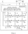
- FIG. 2 there may be an array 28 of memory elements 20 in device 10. There are only three rows and columns of elements 20 in the illustrative array of FIG. 2 , but in general there may be hundreds or thousands of rows and columns in array 28.
- Array 28 may be one of a number of arrays on a given device 10, may be a subarray that is part of a larger array, or may be any other suitable group of memory elements 20.
- Each memory element may supply a corresponding output signal OUT at a corresponding output path 38.
- each signal OUT is a static output control signal that may be conveyed over a path 40 and used in configuring a corresponding transistor such as transistor 18 or other circuit element in associated programmable logic 18.
- Integrated circuit 10 may have control circuitry 24 for supplying signals to memory elements 20 in memory array 28.
- Control circuitry 24 may receive power supply voltages, data, and other signals from external sources using pins 14 and from internal sources using paths such as paths 30.
- Control circuitry 24 may include circuitry such as an adjustable voltage supply (regulator 22), address decoder circuitry, address register circuitry, data register circuitry, and/or clear control circuitry.
- Regulator 22 may be used to produce time-varying power supply voltages. These power supply voltages may be of the same magnitude as the voltages received on pins 14 or may have different magnitudes than the voltage received from pins 14.
- Control circuitry 24 (e.g., the addressing circuitry, data register circuitry, clear control circuitry, and other control circuitry of circuitry 24) can use the power supply voltages supplied by pins 14 and by regulator 22 to produce desired time-varying and fixed signals on paths such as paths 32 and 34.
- each row of array 28 may have one or more associated address lines in a respective one of paths 32 that carries a corresponding address signal (as an example).
- the address lines are sometimes referred to as a word lines, and the address signals are sometimes referred to as word line signals.
- Each column of array 28 may have one or more associated data lines in a respective one of paths 34 on which data signals are provided.
- the data lines are sometimes referred to as bit lines, and the data signals are sometimes referred to as bit line signals. If desired, other patterns of lines may be used in paths 32 and 34.
- the signals that are supplied to memory elements 20 may sometimes be collectively referred to as control signals. In particular contexts, some of these signals may be referred to as power signals, clear signals, data signals, address signals, etc. These different signal types are not mutually exclusive.
- FIG. 2 is a circuit diagram showing one suitable arrangement of memory cell 20.
- the storage portion of cell 20 may include cross-coupled inverting circuits such as circuits INV1 and INV2 each of which has an input and an output.
- the input of circuit INV1 may be coupled to the output of circuit INV2, whereas the input of INV2 may be coupled to the output of circuit INV1.
- the output of circuit INV1 may serve as a first internal data storage node X1 for cell 20 while the output of circuit INV2 may serve as a second internal data storage node X2 for cell 20.
- the storage portion of cell 20 configured in this way may be used to store a single bit of data (e.g., data storage nodes X1 and X2 may store true and complement versions of a single data bit, respectively).
- cell 20 that is storing a high data bit may have data storage nodes X1 and X2 respectively driven to "0" and "1.”
- cell 20 that is storing a low data bit may have data storage nodes X1 and X2 respectively driven to "1" and "0.”
- Node X2 may be coupled to one or more corresponding pass transistor 40 via path 40, which may be part of programmable logic circuitry 18 on device 10.
- Circuit INV1 may include an n-channel transistor N1 and p-channel transistor P1 coupled in series between a first power supply line 100 (e.g., a power supply line on which positive power supply voltage Vcchg is provided) and a second power supply line 102 (e.g., a lower supply line that is supplied with pull-down voltage Vpd). Supply line 102 is therefore sometimes referred to as a pull-down node.
- circuit INV2 may include an n-channel transistor N2 and p-channel transistor P2 coupled in series between power supply lines 100 and 102.
- N-channel transistor N1 and N2 in the pull-down current path may sometimes be referred to as memory "pull-down” devices, whereas p-channel transistors P1 and P2 may sometimes be referred to as memory “pull-up” devices.
- the n-channel transistors may be n-channel metal-oxide-semiconductor (NMOS) devices, whereas the p-channel transistors may be p-channel metal-oxide-semiconductor (PMOS) devices (as an example).
- the storage portion of memory cell 20 may be coupled to access transistors (sometimes referred to as memory address transistors or memory “pass gate” transistors) such as transistors NA1 and NA2 to perform read and write operations.
- access transistor NA1 may be coupled between a first data line (e.g., a true data line on which true bit line signal BL is conveyed) and first data storage node X1
- access transistor NA2 may be coupled between a second data line (e.g., a complementary data line on which complement bit line signal BL/ is conveyed) and second data storage node X2.
- Transistors NA1 and NA2 may each have a gate that is coupled to an address line on which word line signal WL is conveyed.
- the true and complementary data lines may be nominally driven to zero volts to minimize leakage currents, whereas word line signal WL may be deasserted (e.g., address signal WL may be pulled low to disable access transistors NA1 and NA2).
- desired data signals may be presented on the first and second data lines before word line signal WL is asserted to enable access transistors NA1 and NA2 to write in a desired value into memory cell 20.
- the first and second data lines are precharged to a high voltage level before word line signal WL is asserted to enable access transistors NA1 and NA2 to read out a currently stored value in memory cell 20.
- each p-channel transistor in the storage portion of memory cell 20 may have a body terminal that is coupled to control line 101.
- Line 101 may be biased to an n-well tap voltage Vntap.
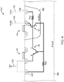
- FIG. 4 is a cross-sectional side view illustrating a parasitic silicon-controlled rectifier (SCR) structure in memory cell 20.
- n-channel transistor N1 may have n+ source-drain regions formed in a p-type semiconductor substrate such as substrate 400
- p-channel transistor P1 may have p+ source-drain regions formed in an n-well such as n-well 402.
- Transistors N1 and P2 are connected in series to form inverter circuit INV1 of FIG. 3 .
- a p-well tap region such as p+ well tap 410 may be formed directly in p-type substrate 400 to serve as the body bias terminal for n-channel transistor N1 and other NMOS transistors sharing the same bulk.
- an n-well tap region such as n+ well tap 412 may be formed directly in n-well 402 to serve as the body bias terminal for p-channel transistor P1 and other PMOS transistors sharing the same n-well 402.
- FIG. 4 also shows intrinsic bipolar junction transistors (BJT) such as BJT devices Q1 and Q2 that can be formed in substrate 400.
- BJT intrinsic bipolar junction transistors
- Components Q1 and Q1 and resistors Rpw and Rnw (marked using bolded lines in FIG. 4 ) represent parasitic components in the circuit formed merely as a byproduct of the CMOS process and are not actual discrete devices intentionally formed by the circuit designer.
- parasitic transistor Q1 may be a PNP bipolar transistor having an emitter (E) terminal coupled to power supply line 100, a base (B) terminal that is coupled to control line 101 via intrinsic n-well resistance Rnw, and a collector (C) terminal.
- Parasitic transistor Q2 may be an NPN bipolar transistor having an emitter terminal coupled to pull-down node 102, a collector terminal coupled to the based terminal of transistor Q1, and a base terminal that is coupled to the collector terminal to Q1 and also to p-well tap region 410 via intrinsic p-well resistance Rpw.
- the PNP transistor and the NPN transistor are stacked in a feedback arrangement commonly referred to as a thyristor or a silicon controlled rectifier (SCR).
- SCR silicon controlled rectifier
- This SCR structure may be particularly prone to latch-up, which is a type of short circuit that can occur one device 10. For example, during a single event latch-up when an alpha particle strikes an internal data storage node in memory cell 20, a node that should otherwise be at zero volts might see a temporary voltage spike. This transient voltage spike might inadvertently turn on one of transistors Q1 or Q2. Eventually, both parasitic transistors are turned on for as long as the SCR structure is forward-biased, which usually leads to breakdown of an internal junction and can permanently damage the device.
- Conventional single event latch-up (SEL) mitigation schemes include reducing the well tap distance to minimize the intrinsic well resistances, increasing well doping to similarly reduce the voltage drop, reducing parasitic transistor gain via transistor sizing and channel doping, reducing the memory cell supply voltage Vcchg, or adding an additional PMOS transistor in the memory cell pull-up path, wherein the additional PMOS transistor is shared among a column of memory cells.
- SEL single event latch-up
- FIG. 5 shows a group of memory cells that is coupled to single event latch-up prevention circuitry such as memory element SEL prevention circuitry 500.
- the group of memory cells may belong to a row of memory cells that are coupled to a common word line in the array or may belong to a column of memory cells that are coupled to a common pair of bit lines in the array.
- SEL prevention circuitry 500 may include a clamping circuit such as clamping circuit 502, a voltage sensing circuit such as voltage sensor 504, and a well tap driver circuit such as well tap driver 506.
- Clamping circuit 502 may allow an internal node voltage in memory cell 20 to rise in response to a single-event perturbation.
- Voltage sensor 504 may be a comparator that picks up a latch-up signal.
- Well tap driver 506 may then force the n-well (e.g., n-well 402 of FIG. 4 ) within memory cell 20 into deep reverse bias region to prevent the latch-up.
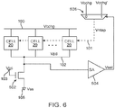
- FIG. 6 is a circuit diagram showing one suitable implementation of latch-up prevention circuitry 500.
- the group of memory cells 20 may be powered using positive power supply line 100 and may also be coupled to a shared pull-down node 102.
- Clamping circuit 502 may be an n-channel clamping transistor having a drain terminal that is connected to node 102, a source terminal that is connected to ground line 105 (e.g., a ground power supply line on which ground voltage Vss is supplied), and a gate terminal that is connected to power supply line 103 (e.g., a power supply line on which positive power supply voltage Vcc is provided).
- Memory cell voltage Vcchg may equal to or greater than power supply voltage Vcc. As an example, voltage Vcc may be equal to 0.85 V, whereas voltage Vcchg may be equal to 1.2 V. Biased as such, clamping transistor 502 is always turned on during normal operation of the integrated circuit.
- Voltage sensing circuit 504 may be a sense amplifier or a voltage comparator having an input that receives voltage Vpd from node 102 and an output at which corresponding control signal Vsel is generated. When node 102 is nominally at zero volts, sense amplifier 504 will keep signal Vsel at a logic "0.” When node 102 rises above a predetermined threshold, sense amplifier 504 will detect the temporary voltage rise and will drive signal Vsel to a logic "1.”
- Signal Vsel output from circuit 504 may be used to control driver circuit 506.
- Driver 506 may be implemented as a multiplexer having a control input that receives signal Vsel, a first (0) data input that receives voltage Vcchg, a second (1) data input that receives voltage Vcchg', and an output on which a selected one of input voltages Vcchg and Vcchg' may be routed. If selected signal Vsel is low, multiplexer 506 may drive its output to Vcchg. If select signal Vsel is high, multiplexer 506 may drive its output to Vcchg'. Voltage Vcchg' may be greater than Vcchg.
- Vcchg' might be equal to 1.8 V.
- elevated voltage Vcchg' may be at least 10%, 20%, 30%, 40%, or 50% greater than voltage Vcchg.
- the output of multiplexer 506 may be connected to the n-well tap of each memory cell 20 in the group via path 101. Thus, the n-well of each memory cell 20 will be biased to either Vcchg or Vcchg' depending on the value of select signal Vsel.
- FIG. 7 is a schematic diagram showing how the SEL prevention circuitry of FIG. 6 is connected to the parasitic SCR structure described above in connection with FIG. 4 .
- Clamping transistor 502 may be connected between emitter of BJT Q2 and the ground line.
- Sensing circuit 504 may be implemented as a comparator having a first (+) terminal that is connected to intrinsic p-well resistance Rpw and a second (-) terminal that receives a reference voltage Vref.
- Voltage level Vref may 0-50 mV or other predetermined reference voltage level suitable for sensing a single-event voltage perturbation.
- the output of driver 506 may be connected to intrinsic n-well resistance Rnw.
- transistor Q1 When voltage Vntap at the output of driver 506 is biased to elevated voltage level Vcchg', transistor Q1 will be shut off since the base-to-emitter voltage V BE of transistor Q1 is now in reverse bias. Turning transistor Q1 off will in turn shut transistor Q2 off since no current can flow to the base of transistor Q2.
- FIG. 8 is a flow chart of illustrative steps for operating memory cell latch-up prevention circuitry 500.
- configuration data may be loaded into memory cells 20 (e.g., via initial device configuration or partial reconfiguration operations). Once loaded with configuration data, memory cells 20 may be used to provide static control signals to control corresponding pass gates in programmable circuitry 18 (step 802). See, e.g., FIGS. 1 and 2 .
- SEL prevention circuitry 500 may be switched out of use until an SEL event is detected.
- a temporary voltage rise may be observed at clamping circuit 502 (step 806).
- sensing circuit 504 may then detect the temporary voltage rise at the clamping circuit.
- sensing circuit 504 may direct well tap driver 506 to provide elevated voltage Vcchg' to the n-well tap region of the pull-up transistors in memory cells 20 to help turn off the parasitic latch-up circuitry (step 808).
- the actual prevention of the single event latch-up may be effectuated by reverse biasing the n-well region in which the memory cell pull-up transistors are formed.
- pull-down node voltage Vpd will be driven back down to ground, and sensing circuit 504 will drive Vsel back down to a logic "0."
- the well tap driver circuit will be configured to provide nominal memory cell voltage Vcchg to the memory cell pull-up transistors so that memory cells 20 can operate as intended (step 810).
- steps are merely illustrative and are not intended to limit the scope of the present embodiments.
- the existing steps may be modified or omitted; some of the steps may be performed in parallel; additional steps may be added; and the order of certain steps may be reversed or altered.
- the n-well tap of each memory cell 20 in the group may be permanently or statically biased to elevated voltage Vcchg' (see, e.g., FIG. 9 ).
- Vcchg' elevated voltage
- FIG. 9 no clamping circuit is needed, so each memory cell 20 may be directly connected to the ground line (i.e., the clamping transistor can be omitted). Since there is no longer a clamping circuit, voltage sensing circuit 504 and multiplexer 506 can likewise be omitted, which further reduces memory cell area.
- This approach permanently prevent SEL at the expense of increased static current leakage and reduced circuit performance (since constantly driving the n-well in reverse bias mode throughout operation of the integrated circuit degrades the drive strength of the memory cell pull-up transistors).
- the selective n-well biasing scheme described above can be implemented in a column or a small block of memory depending on the intended application.
- the reference voltage of the comparator circuit of FIG. 7 can be optimized to reduce the impact of any CRAM leakage increase arising from the reverse biasing step.
- the duration for which multiplexing driver 506 is activated in response to a SEL can be adjusted and optimized for latch-up turn-off and to reduce the impact of transient CRAM leakage increase.
- programmable logic devices include programmable arrays logic (PALs), programmable logic arrays (PLAs), field programmable logic arrays (FPLAs), electrically programmable logic devices (EPLDs), electrically erasable programmable logic devices (EEPLDs), logic cell arrays (LCAs), complex programmable logic devices (CPLDs), and field programmable gate arrays (FPGAs), just to name a few.
- PALs programmable arrays logic
- PLAs programmable logic arrays
- FPLAs field programmable logic arrays
- EPLDs electrically programmable logic devices
- EEPLDs electrically erasable programmable logic devices
- LCAs logic cell arrays
- CPLDs complex programmable logic devices
- FPGAs field programmable gate arrays
- the programmable logic device described in one or more embodiments herein may be part of a data processing system that includes one or more of the following components: a processor; memory; IO circuitry; and peripheral devices.
- the data processing can be used in a wide variety of applications, such as computer networking, data networking, instrumentation, video processing, digital signal processing, or any suitable other application where the advantage of using programmable or re-programmable logic is desirable.
- the programmable logic device can be used to perform a variety of different logic functions.
- the programmable logic device can be configured as a processor or controller that works in cooperation with a system processor.
- the programmable logic device may also be used as an arbiter for arbitrating access to a shared resource in the data processing system.
- the programmable logic device can be configured as an interface between a processor and one of the other components in the system.
- the programmable logic device may be one of the family of devices owned by ALTERA/INTEL Corporation.
Landscapes
- Engineering & Computer Science (AREA)
- Microelectronics & Electronic Packaging (AREA)
- Computer Hardware Design (AREA)
- Power Engineering (AREA)
- Static Random-Access Memory (AREA)
- Semiconductor Integrated Circuits (AREA)
- Semiconductor Memories (AREA)
Abstract
Description
- This relates to integrated circuits and, more particularly, to integrated circuits that contain memory.
- Integrated circuits often contain volatile memory elements. A volatile memory element retains data only so long as the integrated circuit is powered. In the event of power loss, the data in the volatile memory element is lost. Although nonvolatile memory elements such as memory elements based on electrically-erasable programmable read-only memory technology are not subject to data loss in this way, it is often not desirable or possible to fabricate nonvolatile memory elements as part of a given integrated circuit.
- As a result, volatile memory elements are often used. For example, static random-access memory (SRAM) chips contain SRAM cells, which are a type of volatile memory element. In programmable logic device integrated circuits, SRAM cells may serve as configuration random access memory (CRAM) cells. Programmable logic devices are a type of integrated circuit that can be programmed by a user to implement a desired custom logic function. CRAM cells are used to store configuration data supplied by the user. Once loaded, CRAM cells supply control signals to transistors to configure the transistors to implement the desired logic function.
- Volatile memory elements often occupy a significant portion of an integrated circuit and are prone to semiconductor reliability issues such as latch-up. Latch-up is a type of short circuit that can sometime arise between the power supply rails of a memory element. Each memory element includes at least an n-channel transistor coupled to a p-channel transistor, which effectively forms a parasitic silicon-controlled rectifier (SCR) structure in the semiconductor substrate. During a single-event latch-up, heavy ions or protons from cosmic rays or other source of ionizing radiation can strike the SCR, which might cause parasitic bipolar transistors in the SCR to conduct, thereby creating a low resistance path between the positive and ground power supply rails. When this occurs, the latch-up may result in circuit malfunction or potentially destruction of the entire device.
- It is within this context that the embodiments described herein arise.
- An integrated circuit that includes memory cells coupled to single event latch-up (SEL) prevention circuitry is provided. Each memory cell may include cross-coupled inverters and access transistors. Each inverter in the cross-coupled inverters may include an n-channel transistor and a p-channel transistor coupled in series between a positive power supply line and a pull-down node.
- The SEL prevention circuitry may be coupled to the pull-down node and the p-channel transistor of each memory cell. In particular, the SEL prevention circuitry may include a clamping circuit that is connected directly between the pull-down node and a ground power supply line. The clamping circuit may be an n-channel pull-down transistor that is always turned on during normal operation of the integrated circuit.
- The SEL prevention circuitry may also include a voltage sensing circuit having an input that is connected to the pull-down node and an output. The voltage sensing circuit may be implemented as a voltage comparator having a first (positive) input that is directly connected to the pull-down node and a second (negative) input that receives a reference voltage.
- The SEL prevention circuitry may further include a driver circuit that is controlled by the output of the voltage comparator. The driver circuit may be a multiplexing circuit that is configured to provide a selected one of a positive power supply voltage and an elevated power supply voltage to the p-channel transistor in each memory cell. For instance, the p-channel transistor may be formed in an n-well, an n-well tap may be formed in the n-well, and the n-well tap may be actively driven by the multiplexer. The elevated power supply voltage may be at least 30%, at least 40%, or at least 50% greater than the positive power supply voltage. The multiplexer may bias the n-well using the positive power supply voltage most of the time. In response to a single event latch-up, however, the multiplexer may bias the n-well using the elevated power supply voltage to force the n-well into deep reverse bias to mitigate any potential latch-up in the memory cell. Alternatively, the n-well may be permanently biased to the elevated power supply voltage level to reduce circuit complexity.
- Further features of the invention, its nature and various advantages will be more apparent from the accompanying drawings and following detailed description.
-
-
FIG. 1 is a diagram of an illustrative programmable integrated circuit in accordance with an embodiment. -
FIG. 2 is a diagram of an illustrative array of memory cells in accordance with an embodiment. -
FIG. 3 is a circuit diagram of an illustrative memory cell in accordance with an embodiment. -
FIG. 4 is a cross-sectional side view illustrating a parasitic silicon-controlled rectifier (SCR) structure in accordance with an embodiment. -
FIG. 5 is a diagram of a group of memory cells that is coupled to single event latch-up prevention circuitry in accordance with an embodiment. -
FIG. 6 is a circuit diagram showing one suitable implementation of latch-up prevention circuitry in accordance with an embodiment. -
FIG. 7 is a diagram illustrating how the latch-up prevention circuitry ofFIG. 6 can be used to turn off the parasitic SCR structure in a memory element in accordance with an embodiment. -
FIG. 8 is a flow chart of illustrative steps for operating memory cell latch-up prevention circuitry in accordance with an embodiment. -
FIG. 9 is a diagram showing how an n-well tap for a group of memory cells can be biased to a fixed, elevated voltage level to permanently shut off the parasitic SCR structure in accordance with an embodiment. - Embodiments of the present invention relate to integrated circuit memory elements that may be subject to single event latch-up (SEL). In accordance with an embodiment, SEL prevention circuitry is provided that uses a sense amplifier to detect a latch-up signal. In response to detecting a latch-up signal, a driver in the SEL prevention circuitry may then force an n-well within the memory elements into deep reverse bias region to temporarily turn off any parasitic components which might be turned on during the single event latch-up. In another suitable arrangement, the n-well of the memory elements may be constantly biased to an elevated voltage level to permanently shut off the parasitic components to completely eliminate latch-up.
- It will be recognized by one skilled in the art, that the present exemplary embodiments may be practiced without some or all of these specific details. In other instances, well-known operations have not been described in detail in order not to unnecessarily obscure the present embodiments.
- The memory elements can be used in any suitable integrated circuits that use memory. These integrated circuits may be memory chips, digital signal processing circuits with memory arrays, microprocessors, application specific integrated circuits with memory arrays, programmable integrated circuits such as programmable logic device integrated circuits in which memory elements are used for configuration memory, or any other suitable integrated circuit. For clarity, the present invention will sometimes be described in the context of programmable logic device integrated circuits. This is, however, merely illustrative. Memory cells in accordance with embodiments of the present invention may be used in any suitable circuits.
- On integrated circuits such as memory chips or other circuits in which memory is needed to store processing data,
memory elements 20 perform the functions of static random-access memory (RAM) cells and are sometimes referred to as SRAM cells. In the context of programmable logic device integrated circuits, the memory elements can be used to store configuration data and are therefore sometimes referred to in this context as configuration random-access memory (CRAM) cells. - An illustrative integrated circuit such as a
programmable logic device 10 is shown inFIG. 1 .Device 10 may have input/output circuitry 12 for driving signals off ofdevice 10 and for receiving signals from other devices via input/output pins 14.Interconnection resources 16 such as global and local vertical and horizontal conductive lines and busses may be used to route signals ondevice 10.Interconnection resources 16 include fixed interconnects (conductive lines) and programmable interconnects (i.e., programmable connections between respective fixed interconnects).Programmable logic 18 may include combinational and sequential logic circuitry. Theprogrammable logic 18 may be configured to perform a custom logic function. The programmable interconnects associated with interconnection resources may be considered to be a part ofprogrammable logic 18. -
Programmable logic device 10 containsvolatile memory elements 20 that can be loaded with configuration data (also called programming data) usingpins 14 and input-output circuitry 12. Once loaded, the memory elements each provide a corresponding static control output signal that controls the state of an associated logic component inprogrammable logic 18. If desired,memory elements 20 may be used in SRAM-type memory arrays (e.g., to store data for processing circuitry during operation of device 10). - Each
memory element 20 may be formed from a number of transistors configured to form a bistable circuit. With one suitable approach, complementary metal-oxide-semiconductor (CMOS) integrated circuit technology is used to form thememory elements 20, so CMOS-based memory element implementations are described herein as an example. If desired, other integrated circuit technologies may be used to form the memory elements and the integrated circuit in which the memory elements are used to form memory arrays. - The memory elements may be loaded from an external erasable-programmable read-only memory and control chip or other suitable data source via
pins 14 and input/output circuitry 12. LoadedCRAM memory elements 20 may provide static control signals that are applied to the terminals (e.g., gates) of circuit elements (e.g., metal-oxide-semiconductor transistors) inprogrammable logic 18 to control those elements (e.g., to turn certain transistors on or off) and thereby configure the logic inprogrammable logic 18. The circuit elements may be transistors such as pass transistors, parts of multiplexers, look-up tables, logic arrays, AND, OR, NAND, and NOR logic gates, etc. - The
memory elements 20 may be arranged in an array pattern. In a typical modern programmable logic device, there may be millions ofmemory elements 20 on each chip. During programming operations, the array of memory elements is provided with configuration data by a user (e.g., a logic designer). Once loaded with configuration data, thememory elements 20 selectively control portions of the circuitry in theprogrammable logic 18 and thereby customize its functions so that it will operate as desired. - When
memory elements 20 are arranged in an array, horizontal and vertical conductors and associated loading circuitry may be used to load the memory elements with configuration data. Any suitable memory array architecture may be used formemory elements 20. One suitable arrangement is shown inFIG. 2 . As shown inFIG. 2 , there may be anarray 28 ofmemory elements 20 indevice 10. There are only three rows and columns ofelements 20 in the illustrative array ofFIG. 2 , but in general there may be hundreds or thousands of rows and columns inarray 28.Array 28 may be one of a number of arrays on a givendevice 10, may be a subarray that is part of a larger array, or may be any other suitable group ofmemory elements 20. Each memory element may supply a corresponding output signal OUT at acorresponding output path 38. In CRAM arrays, each signal OUT is a static output control signal that may be conveyed over apath 40 and used in configuring a corresponding transistor such astransistor 18 or other circuit element in associatedprogrammable logic 18. - Integrated
circuit 10 may havecontrol circuitry 24 for supplying signals tomemory elements 20 inmemory array 28.Control circuitry 24 may receive power supply voltages, data, and other signals from externalsources using pins 14 and from internal sources using paths such aspaths 30.Control circuitry 24 may include circuitry such as an adjustable voltage supply (regulator 22), address decoder circuitry, address register circuitry, data register circuitry, and/or clear control circuitry.Regulator 22 may be used to produce time-varying power supply voltages. These power supply voltages may be of the same magnitude as the voltages received onpins 14 or may have different magnitudes than the voltage received frompins 14. Control circuitry 24 (e.g., the addressing circuitry, data register circuitry, clear control circuitry, and other control circuitry of circuitry 24) can use the power supply voltages supplied bypins 14 and byregulator 22 to produce desired time-varying and fixed signals on paths such aspaths - There may, in general, be any suitable number of conductive lines associated with
paths array 28 may have one or more associated address lines in a respective one ofpaths 32 that carries a corresponding address signal (as an example). The address lines are sometimes referred to as a word lines, and the address signals are sometimes referred to as word line signals. Each column ofarray 28 may have one or more associated data lines in a respective one ofpaths 34 on which data signals are provided. The data lines are sometimes referred to as bit lines, and the data signals are sometimes referred to as bit line signals. If desired, other patterns of lines may be used inpaths memory elements 20 may sometimes be collectively referred to as control signals. In particular contexts, some of these signals may be referred to as power signals, clear signals, data signals, address signals, etc. These different signal types are not mutually exclusive. -
FIG. 2 is a circuit diagram showing one suitable arrangement ofmemory cell 20. As shown inFIG. 2 , the storage portion ofcell 20 may include cross-coupled inverting circuits such as circuits INV1 and INV2 each of which has an input and an output. In particular, the input of circuit INV1 may be coupled to the output of circuit INV2, whereas the input of INV2 may be coupled to the output of circuit INV1. The output of circuit INV1 may serve as a first internal data storage node X1 forcell 20 while the output of circuit INV2 may serve as a second internal data storage node X2 forcell 20. The storage portion ofcell 20 configured in this way may be used to store a single bit of data (e.g., data storage nodes X1 and X2 may store true and complement versions of a single data bit, respectively). As an example,cell 20 that is storing a high data bit may have data storage nodes X1 and X2 respectively driven to "0" and "1." As another example,cell 20 that is storing a low data bit may have data storage nodes X1 and X2 respectively driven to "1" and "0." Node X2 may be coupled to one or morecorresponding pass transistor 40 viapath 40, which may be part ofprogrammable logic circuitry 18 ondevice 10. - Circuit INV1 may include an n-channel transistor N1 and p-channel transistor P1 coupled in series between a first power supply line 100 (e.g., a power supply line on which positive power supply voltage Vcchg is provided) and a second power supply line 102 (e.g., a lower supply line that is supplied with pull-down voltage Vpd).
Supply line 102 is therefore sometimes referred to as a pull-down node. Similarly, circuit INV2 may include an n-channel transistor N2 and p-channel transistor P2 coupled in series betweenpower supply lines - The storage portion of
memory cell 20 may be coupled to access transistors (sometimes referred to as memory address transistors or memory "pass gate" transistors) such as transistors NA1 and NA2 to perform read and write operations. In the example ofFIG. 3 , access transistor NA1 may be coupled between a first data line (e.g., a true data line on which true bit line signal BL is conveyed) and first data storage node X1, whereas access transistor NA2 may be coupled between a second data line (e.g., a complementary data line on which complement bit line signal BL/ is conveyed) and second data storage node X2. Transistors NA1 and NA2 may each have a gate that is coupled to an address line on which word line signal WL is conveyed. - During normal operation, the true and complementary data lines may be nominally driven to zero volts to minimize leakage currents, whereas word line signal WL may be deasserted (e.g., address signal WL may be pulled low to disable access transistors NA1 and NA2). During write operations, desired data signals may be presented on the first and second data lines before word line signal WL is asserted to enable access transistors NA1 and NA2 to write in a desired value into
memory cell 20. During read operations, the first and second data lines are precharged to a high voltage level before word line signal WL is asserted to enable access transistors NA1 and NA2 to read out a currently stored value inmemory cell 20. - Still referring to
FIG. 3 , each p-channel transistor in the storage portion ofmemory cell 20 may have a body terminal that is coupled to controlline 101.Line 101 may be biased to an n-well tap voltage Vntap. By dynamically adjusting the voltage level of signal Vntap, potential latch-up issues that may occur inmemory cell 20 may be mitigated. -
FIG. 4 is a cross-sectional side view illustrating a parasitic silicon-controlled rectifier (SCR) structure inmemory cell 20. As shown inFIG. 4 , n-channel transistor N1 may have n+ source-drain regions formed in a p-type semiconductor substrate such assubstrate 400, whereas p-channel transistor P1 may have p+ source-drain regions formed in an n-well such as n-well 402. Transistors N1 and P2 are connected in series to form inverter circuit INV1 ofFIG. 3 . A p-well tap region such as p+ well tap 410 may be formed directly in p-type substrate 400 to serve as the body bias terminal for n-channel transistor N1 and other NMOS transistors sharing the same bulk. Similarly, an n-well tap region such as n+ well tap 412 may be formed directly in n-well 402 to serve as the body bias terminal for p-channel transistor P1 and other PMOS transistors sharing the same n-well 402. -
FIG. 4 also shows intrinsic bipolar junction transistors (BJT) such as BJT devices Q1 and Q2 that can be formed insubstrate 400. Components Q1 and Q1 and resistors Rpw and Rnw (marked using bolded lines inFIG. 4 ) represent parasitic components in the circuit formed merely as a byproduct of the CMOS process and are not actual discrete devices intentionally formed by the circuit designer. In particular, parasitic transistor Q1 may be a PNP bipolar transistor having an emitter (E) terminal coupled topower supply line 100, a base (B) terminal that is coupled to controlline 101 via intrinsic n-well resistance Rnw, and a collector (C) terminal. Parasitic transistor Q2 may be an NPN bipolar transistor having an emitter terminal coupled to pull-down node 102, a collector terminal coupled to the based terminal of transistor Q1, and a base terminal that is coupled to the collector terminal to Q1 and also to p-well tap region 410 via intrinsic p-well resistance Rpw. - Configured in this way, the PNP transistor and the NPN transistor are stacked in a feedback arrangement commonly referred to as a thyristor or a silicon controlled rectifier (SCR). This SCR structure may be particularly prone to latch-up, which is a type of short circuit that can occur one
device 10. For example, during a single event latch-up when an alpha particle strikes an internal data storage node inmemory cell 20, a node that should otherwise be at zero volts might see a temporary voltage spike. This transient voltage spike might inadvertently turn on one of transistors Q1 or Q2. Eventually, both parasitic transistors are turned on for as long as the SCR structure is forward-biased, which usually leads to breakdown of an internal junction and can permanently damage the device. - Conventional single event latch-up (SEL) mitigation schemes include reducing the well tap distance to minimize the intrinsic well resistances, increasing well doping to similarly reduce the voltage drop, reducing parasitic transistor gain via transistor sizing and channel doping, reducing the memory cell supply voltage Vcchg, or adding an additional PMOS transistor in the memory cell pull-up path, wherein the additional PMOS transistor is shared among a column of memory cells. These techniques, however, typically increase die area and reduces maximum memory performance. It would therefore be desirable to provide an improved way of mitigating SEL.
- In accordance with an embodiment,
FIG. 5 shows a group of memory cells that is coupled to single event latch-up prevention circuitry such as memory elementSEL prevention circuitry 500. The group of memory cells may belong to a row of memory cells that are coupled to a common word line in the array or may belong to a column of memory cells that are coupled to a common pair of bit lines in the array. - As shown in
FIG. 5 ,SEL prevention circuitry 500 may include a clamping circuit such as clampingcircuit 502, a voltage sensing circuit such asvoltage sensor 504, and a well tap driver circuit such aswell tap driver 506. Clampingcircuit 502 may allow an internal node voltage inmemory cell 20 to rise in response to a single-event perturbation.Voltage sensor 504 may be a comparator that picks up a latch-up signal. Welltap driver 506 may then force the n-well (e.g., n-well 402 ofFIG. 4 ) withinmemory cell 20 into deep reverse bias region to prevent the latch-up. -
FIG. 6 is a circuit diagram showing one suitable implementation of latch-upprevention circuitry 500. As shown inFIG. 6 , the group ofmemory cells 20 may be powered using positivepower supply line 100 and may also be coupled to a shared pull-down node 102. Clampingcircuit 502 may be an n-channel clamping transistor having a drain terminal that is connected tonode 102, a source terminal that is connected to ground line 105 (e.g., a ground power supply line on which ground voltage Vss is supplied), and a gate terminal that is connected to power supply line 103 (e.g., a power supply line on which positive power supply voltage Vcc is provided). Memory cell voltage Vcchg may equal to or greater than power supply voltage Vcc. As an example, voltage Vcc may be equal to 0.85 V, whereas voltage Vcchg may be equal to 1.2 V. Biased as such, clampingtransistor 502 is always turned on during normal operation of the integrated circuit. -
Voltage sensing circuit 504 may be a sense amplifier or a voltage comparator having an input that receives voltage Vpd fromnode 102 and an output at which corresponding control signal Vsel is generated. Whennode 102 is nominally at zero volts,sense amplifier 504 will keep signal Vsel at a logic "0." Whennode 102 rises above a predetermined threshold,sense amplifier 504 will detect the temporary voltage rise and will drive signal Vsel to a logic "1." - Signal Vsel output from
circuit 504 may be used to controldriver circuit 506.Driver 506 may be implemented as a multiplexer having a control input that receives signal Vsel, a first (0) data input that receives voltage Vcchg, a second (1) data input that receives voltage Vcchg', and an output on which a selected one of input voltages Vcchg and Vcchg' may be routed. If selected signal Vsel is low,multiplexer 506 may drive its output to Vcchg. If select signal Vsel is high,multiplexer 506 may drive its output to Vcchg'. Voltage Vcchg' may be greater than Vcchg. For example, if Vcchg is 1.2 V, Vcchg' might be equal to 1.8 V. In general, elevated voltage Vcchg' may be at least 10%, 20%, 30%, 40%, or 50% greater than voltage Vcchg. The output ofmultiplexer 506 may be connected to the n-well tap of eachmemory cell 20 in the group viapath 101. Thus, the n-well of eachmemory cell 20 will be biased to either Vcchg or Vcchg' depending on the value of select signal Vsel. - Configured in this way, a random particle strike that might potentially cause a circuit latch-up will force an internal data storage node in one of
memory cells 20 to rise, which will in turn result in a temporarily voltage rise atnode 102. When pull-down node voltage Vpd atnode 102 rises,sense amplifier 504 will detect the instantaneous voltage rise, which will then drive control signal Vsel high. When signal Vsel is driven high,multiplexer 506 may then drive n-well tap voltage Vntap to elevated voltage level Vcchg', which reverse biases the n-well region, thereby shutting off the parasitic bipolar junction transistors in the SCR structure. -
FIG. 7 is a schematic diagram showing how the SEL prevention circuitry ofFIG. 6 is connected to the parasitic SCR structure described above in connection withFIG. 4 . Clampingtransistor 502 may be connected between emitter of BJT Q2 and the ground line.Sensing circuit 504 may be implemented as a comparator having a first (+) terminal that is connected to intrinsic p-well resistance Rpw and a second (-) terminal that receives a reference voltage Vref. Voltage level Vref may 0-50 mV or other predetermined reference voltage level suitable for sensing a single-event voltage perturbation. The output ofdriver 506 may be connected to intrinsic n-well resistance Rnw. When voltage Vntap at the output ofdriver 506 is biased to elevated voltage level Vcchg', transistor Q1 will be shut off since the base-to-emitter voltage VBE of transistor Q1 is now in reverse bias. Turning transistor Q1 off will in turn shut transistor Q2 off since no current can flow to the base of transistor Q2. -
FIG. 8 is a flow chart of illustrative steps for operating memory cell latch-upprevention circuitry 500. Atstep 800, configuration data may be loaded into memory cells 20 (e.g., via initial device configuration or partial reconfiguration operations). Once loaded with configuration data,memory cells 20 may be used to provide static control signals to control corresponding pass gates in programmable circuitry 18 (step 802). See, e.g.,FIGS. 1 and2 . -
SEL prevention circuitry 500 may be switched out of use until an SEL event is detected. In response tomemory cell 20 receiving a heavy ion strike, a temporary voltage rise may be observed at clamping circuit 502 (step 806). Atstep 806,sensing circuit 504 may then detect the temporary voltage rise at the clamping circuit. - In response to detecting the voltage rise,
sensing circuit 504 may direct well tapdriver 506 to provide elevated voltage Vcchg' to the n-well tap region of the pull-up transistors inmemory cells 20 to help turn off the parasitic latch-up circuitry (step 808). The actual prevention of the single event latch-up may be effectuated by reverse biasing the n-well region in which the memory cell pull-up transistors are formed. - After the temporarily voltage perturbation dissipates, pull-down node voltage Vpd will be driven back down to ground, and
sensing circuit 504 will drive Vsel back down to a logic "0." As a result, the well tap driver circuit will be configured to provide nominal memory cell voltage Vcchg to the memory cell pull-up transistors so thatmemory cells 20 can operate as intended (step 810). - These steps are merely illustrative and are not intended to limit the scope of the present embodiments. The existing steps may be modified or omitted; some of the steps may be performed in parallel; additional steps may be added; and the order of certain steps may be reversed or altered.
- In another suitable arrangement, the n-well tap of each
memory cell 20 in the group may be permanently or statically biased to elevated voltage Vcchg' (see, e.g.,FIG. 9 ). As shown inFIG. 9 , no clamping circuit is needed, so eachmemory cell 20 may be directly connected to the ground line (i.e., the clamping transistor can be omitted). Since there is no longer a clamping circuit,voltage sensing circuit 504 andmultiplexer 506 can likewise be omitted, which further reduces memory cell area. This approach permanently prevent SEL at the expense of increased static current leakage and reduced circuit performance (since constantly driving the n-well in reverse bias mode throughout operation of the integrated circuit degrades the drive strength of the memory cell pull-up transistors). - If desired, the selective n-well biasing scheme described above can be implemented in a column or a small block of memory depending on the intended application. The reference voltage of the comparator circuit of
FIG. 7 can be optimized to reduce the impact of any CRAM leakage increase arising from the reverse biasing step. Moreover, the duration for which multiplexingdriver 506 is activated in response to a SEL can be adjusted and optimized for latch-up turn-off and to reduce the impact of transient CRAM leakage increase. - The embodiments thus far have been described with respect to integrated circuits. The methods and apparatuses described herein may be incorporated into any suitable circuit. For example, they may be incorporated into numerous types of devices such as programmable logic devices, application specific standard products (ASSPs), and application specific integrated circuits (ASICs). Examples of programmable logic devices include programmable arrays logic (PALs), programmable logic arrays (PLAs), field programmable logic arrays (FPLAs), electrically programmable logic devices (EPLDs), electrically erasable programmable logic devices (EEPLDs), logic cell arrays (LCAs), complex programmable logic devices (CPLDs), and field programmable gate arrays (FPGAs), just to name a few.
- The programmable logic device described in one or more embodiments herein may be part of a data processing system that includes one or more of the following components: a processor; memory; IO circuitry; and peripheral devices. The data processing can be used in a wide variety of applications, such as computer networking, data networking, instrumentation, video processing, digital signal processing, or any suitable other application where the advantage of using programmable or re-programmable logic is desirable. The programmable logic device can be used to perform a variety of different logic functions. For example, the programmable logic device can be configured as a processor or controller that works in cooperation with a system processor. The programmable logic device may also be used as an arbiter for arbitrating access to a shared resource in the data processing system. In yet another example, the programmable logic device can be configured as an interface between a processor and one of the other components in the system. In one embodiment, the programmable logic device may be one of the family of devices owned by ALTERA/INTEL Corporation.
- The foregoing is merely illustrative of the principles of this invention and various modifications can be made by those skilled in the art. The foregoing embodiments may be implemented individually or in any combination.
Claims (15)
- An integrated circuit, comprising:a memory cell that includes an n-channel transistor and a p-channel transistor coupled in series between a power supply line and a pull-down node; andsingle event latch-up prevention circuitry that is connected to the pull-down node and the p-channel transistor in the memory cell.
- The integrated circuit of claim 1, wherein the single event latch-up prevention circuitry comprises:a clamping circuit that is connected between the pull-down node and a ground line.
- The integrated circuit of claim 2, wherein the clamping circuit comprises another n-channel transistor that is always turned on during normal operation of the integrated circuit.
- The integrated circuit of any one of claims 1-3, wherein the single event latch-up prevention circuitry comprises:a voltage sensing circuit having an input that is connected to the pull-down node and an output.
- The integrated circuit of claim 4, wherein the voltage sensing circuit comprises a comparator having a first input that is directly connected to the pull-down node and a second input that receives a reference voltage.
- The integrated circuit of claim 4, wherein the single event latch-up prevention circuitry further comprises:a driver circuit that receives a control signal from the output of the voltage sensing circuit and that provides a selected one of first and second voltages to the p-channel transistor in the memory cell.
- The integrated circuit of claim 6, wherein the driver circuit comprises a multiplexer having a first input that receives the first voltage, a second input that receives the second voltage, and an output that is coupled to the p-channel transistor in the memory cell.
- The integrated circuit of claim 7, wherein the first voltage is biased at a positive power supply voltage level, and wherein the second voltage is at least 30% greater than the first voltage.
- The integrated circuit of any one of claims 1-8, wherein the p-channel transistor is formed in an n-well, the integrated circuit further comprising:an n-well tap formed in the n-well that is directly driven by the single event latch-up prevention circuitry.
- The integrated circuit of any one of claims 1-9, further comprising:an additional memory cell that includes another n-channel transistor and another p-channel transistor coupled in series between the power supply line and the pull-down node, wherein the p-channel transistor and the another p-channel transistor have body terminals that are connected to the single event latch-up prevention circuitry.
- A method of operating an integrated circuit that includes a memory cell that is coupled to single event latch-up prevention circuitry, the method comprising:loading data onto the memory cell;with the single event latch-up prevention circuitry, detecting for a single event latch-up in the memory cell; andin response to detecting the single event latch-up, activating the single event latch-up prevention circuitry to mitigate the single event latch-up in the memory cell.
- The method of claim 11, wherein detecting for the single event latch-up comprises outputting a temporary voltage rise at a clamping circuit in the single event latch-up prevention circuitry, and wherein detecting for the single event latch-up further comprises determining whether the temporary voltage rise exceeds a predetermined threshold level.
- The method of any one of claims 11-12, further comprising:while the single event latch-up prevention circuitry is deactivated, using the single event latch-up prevention circuitry to provide a first voltage to an n-well in the memory cell, wherein activating the single event latch-up prevention circuitry comprises using the single event latch-up prevention circuitry to provide a second voltage that is greater than that first voltage to the n-well in the memory cell.
- The method of claim 13, wherein the second voltage is at least 40% greater than the first voltage.
- The method of claim 13, wherein the using the single event latch-up prevention circuitry to provide the second voltage to the n-well comprises reverse biasing the n-well.
Applications Claiming Priority (1)
| Application Number | Priority Date | Filing Date | Title |
|---|---|---|---|
| US15/382,095 US10204906B2 (en) | 2016-12-16 | 2016-12-16 | Memory with single-event latchup prevention circuitry |
Publications (2)
| Publication Number | Publication Date |
|---|---|
| EP3336846A1 true EP3336846A1 (en) | 2018-06-20 |
| EP3336846B1 EP3336846B1 (en) | 2020-12-30 |
Family
ID=60382095
Family Applications (1)
| Application Number | Title | Priority Date | Filing Date |
|---|---|---|---|
| EP17201976.2A Active EP3336846B1 (en) | 2016-12-16 | 2017-11-15 | Memory with single-event latchup prevention circuitry |
Country Status (3)
| Country | Link |
|---|---|
| US (1) | US10204906B2 (en) |
| EP (1) | EP3336846B1 (en) |
| CN (1) | CN108206036B (en) |
Families Citing this family (8)
| Publication number | Priority date | Publication date | Assignee | Title |
|---|---|---|---|---|
| US10289178B1 (en) * | 2017-04-04 | 2019-05-14 | Xilinx, Inc. | Configurable single event latch-up (SEL) and electrical overvoltage stress (EOS) detection circuit |
| TWI739091B (en) * | 2018-06-27 | 2021-09-11 | 台灣積體電路製造股份有限公司 | Selection circuitries and method for preventing latch-up of memory storage system |
| US10878852B2 (en) * | 2018-06-27 | 2020-12-29 | Taiwan Semiconductor Manufacturing Co., Ltd. | Latch-up prevention circuit for memory storage system |
| US11030346B2 (en) * | 2018-07-13 | 2021-06-08 | Ememory Technology Inc. | Integrated circuit and data processing method for enhancing security of the integrated circuit |
| AR116929A1 (en) | 2019-10-31 | 2021-06-30 | Invap S E | METHOD TO UPDATE THE REFERENCE THRESHOLD OF AT LEAST ONE OPERATING PARAMETER, PROTECTION UNIT FOR THE MITIGATION OF A SIMPLE LATCHUP EVENT (SEL) IN AN ELECTRONIC DEVICE USING THE REFERENCE THRESHOLD AND ARRANGEMENT FOR THE SIMPLE LATCHUP EVENT SEL) IN A SET |
| CN115372787A (en) * | 2021-05-19 | 2022-11-22 | 长鑫存储技术有限公司 | Test structure of integrated circuit |
| US12112820B2 (en) * | 2021-12-01 | 2024-10-08 | University Of Utah Research Foundation | Single event effect mitigation with smart-redundancy |
| JP2026511858A (en) * | 2023-03-30 | 2026-04-14 | シルバコ・インク | Selective source bias in memory peripherals |
Citations (3)
| Publication number | Priority date | Publication date | Assignee | Title |
|---|---|---|---|---|
| US4791317A (en) * | 1986-09-26 | 1988-12-13 | Siemens Aktiengesellschaft | Latch-up protection circuit for integrated circuits using complementary mos circuit technology |
| US20090244954A1 (en) * | 2008-03-26 | 2009-10-01 | Cannon Ethan H | Structure and method for improving storage latch susceptibility to single event upsets |
| US20140167102A1 (en) * | 2012-07-27 | 2014-06-19 | Freescale Semiconductor, Inc. | Semiconductor device with single-event latch-up prevention circuitry |
Family Cites Families (22)
| Publication number | Priority date | Publication date | Assignee | Title |
|---|---|---|---|---|
| US3434114A (en) | 1966-09-23 | 1969-03-18 | Ibm | Variable floating point precision |
| JPS6238591A (en) * | 1985-08-14 | 1987-02-19 | Fujitsu Ltd | Complementary semiconductor memory device |
| JP2573392B2 (en) * | 1990-03-30 | 1997-01-22 | 株式会社東芝 | Semiconductor storage device |
| JP2530055B2 (en) * | 1990-08-30 | 1996-09-04 | 株式会社東芝 | Semiconductor integrated circuit |
| US5696711A (en) | 1995-12-22 | 1997-12-09 | Intel Corporation | Apparatus and method for performing variable precision floating point rounding operations |
| US6442060B1 (en) * | 2000-05-09 | 2002-08-27 | Monolithic System Technology, Inc. | High-density ratio-independent four-transistor RAM cell fabricated with a conventional logic process |
| US6878595B2 (en) * | 2003-01-27 | 2005-04-12 | Full Circle Research, Inc. | Technique for suppression of latchup in integrated circuits (ICS) |
| US7304354B2 (en) * | 2004-02-17 | 2007-12-04 | Silicon Space Technology Corp. | Buried guard ring and radiation hardened isolation structures and fabrication methods |
| US9842629B2 (en) | 2004-06-25 | 2017-12-12 | Cypress Semiconductor Corporation | Memory cell array latchup prevention |
| JP5100035B2 (en) * | 2005-08-02 | 2012-12-19 | ルネサスエレクトロニクス株式会社 | Semiconductor memory device |
| US8706790B1 (en) | 2009-03-03 | 2014-04-22 | Altera Corporation | Implementing mixed-precision floating-point operations in a programmable integrated circuit device |
| US20110013467A1 (en) * | 2009-07-14 | 2011-01-20 | Vns Portfolio Llc | System and Method for Reading Memory |
| US8482963B1 (en) * | 2009-12-02 | 2013-07-09 | Altera Corporation | Integrated circuits with asymmetric and stacked transistors |
| US9496268B2 (en) * | 2009-12-02 | 2016-11-15 | Altera Corporation | Integrated circuits with asymmetric and stacked transistors |
| US8432724B2 (en) * | 2010-04-02 | 2013-04-30 | Altera Corporation | Memory elements with soft error upset immunity |
| US8369175B1 (en) * | 2010-09-01 | 2013-02-05 | Altera Corporation | Memory elements with voltage overstress protection |
| US8949298B1 (en) | 2011-09-16 | 2015-02-03 | Altera Corporation | Computing floating-point polynomials in an integrated circuit device |
| US9098332B1 (en) | 2012-06-01 | 2015-08-04 | Altera Corporation | Specialized processing block with fixed- and floating-point structures |
| US9104474B2 (en) | 2012-12-28 | 2015-08-11 | Intel Corporation | Variable precision floating point multiply-add circuit |
| US9189200B1 (en) | 2013-03-14 | 2015-11-17 | Altera Corporation | Multiple-precision processing block in a programmable integrated circuit device |
| CN104282331B (en) * | 2013-07-11 | 2017-08-25 | 北京大学 | A kind of adaptive soft fault preventing memory cell and storage circuit |
| CN103474092B (en) * | 2013-09-04 | 2016-01-06 | 华中科技大学 | Radiation hardening storage unit circuit |
-
2016
- 2016-12-16 US US15/382,095 patent/US10204906B2/en active Active
-
2017
- 2017-11-15 EP EP17201976.2A patent/EP3336846B1/en active Active
- 2017-11-16 CN CN201711134937.8A patent/CN108206036B/en active Active
Patent Citations (3)
| Publication number | Priority date | Publication date | Assignee | Title |
|---|---|---|---|---|
| US4791317A (en) * | 1986-09-26 | 1988-12-13 | Siemens Aktiengesellschaft | Latch-up protection circuit for integrated circuits using complementary mos circuit technology |
| US20090244954A1 (en) * | 2008-03-26 | 2009-10-01 | Cannon Ethan H | Structure and method for improving storage latch susceptibility to single event upsets |
| US20140167102A1 (en) * | 2012-07-27 | 2014-06-19 | Freescale Semiconductor, Inc. | Semiconductor device with single-event latch-up prevention circuitry |
Also Published As
| Publication number | Publication date |
|---|---|
| US10204906B2 (en) | 2019-02-12 |
| US20180175033A1 (en) | 2018-06-21 |
| CN108206036A (en) | 2018-06-26 |
| CN108206036B (en) | 2023-05-23 |
| EP3336846B1 (en) | 2020-12-30 |
Similar Documents
| Publication | Publication Date | Title |
|---|---|---|
| EP3336846B1 (en) | Memory with single-event latchup prevention circuitry | |
| US8482965B2 (en) | Volatile memory elements with soft error upset immunity | |
| US8711614B1 (en) | Memory elements with increased write margin and soft error upset immunity | |
| EP1840965B1 (en) | Adjustable transistor body bias generation circuitry with latch-up prevention | |
| US7633830B2 (en) | Reduced leakage driver circuit and memory device employing same | |
| US8530976B1 (en) | Memory element transistors with reversed-workfunction gate conductors | |
| US8842488B2 (en) | Low voltage efuse programming circuit and method | |
| US7826301B2 (en) | Word line driver circuit with reduced leakage | |
| US9767892B1 (en) | Memory elements with dynamic pull-up weakening write assist circuitry | |
| US5892377A (en) | Method and apparatus for reducing leakage currents in an I/O buffer | |
| KR910006478B1 (en) | Semiconductor integrated circuit | |
| US9755647B1 (en) | Techniques for handling high voltage circuitry in an integrated circuit | |
| US9646680B2 (en) | Power gate for latch-up prevention | |
| US7893716B1 (en) | Hotsocket detection circuitry | |
| JP2008244071A (en) | Semiconductor integrated circuit provided with esd protection circuit | |
| US11169590B2 (en) | Core ramp detection circuitry | |
| US8013632B1 (en) | Integrated circuit with global hotsocket architecture | |
| US10242732B2 (en) | Memory elements with soft-error-upset (SEU) immunity using parasitic components |
Legal Events
| Date | Code | Title | Description |
|---|---|---|---|
| PUAI | Public reference made under article 153(3) epc to a published international application that has entered the european phase |
Free format text: ORIGINAL CODE: 0009012 |
|
| STAA | Information on the status of an ep patent application or granted ep patent |
Free format text: STATUS: REQUEST FOR EXAMINATION WAS MADE |
|
| 17P | Request for examination filed |
Effective date: 20171115 |
|
| AK | Designated contracting states |
Kind code of ref document: A1 Designated state(s): AL AT BE BG CH CY CZ DE DK EE ES FI FR GB GR HR HU IE IS IT LI LT LU LV MC MK MT NL NO PL PT RO RS SE SI SK SM TR |
|
| AX | Request for extension of the european patent |
Extension state: BA ME |
|
| STAA | Information on the status of an ep patent application or granted ep patent |
Free format text: STATUS: EXAMINATION IS IN PROGRESS |
|
| 17Q | First examination report despatched |
Effective date: 20190212 |
|
| GRAJ | Information related to disapproval of communication of intention to grant by the applicant or resumption of examination proceedings by the epo deleted |
Free format text: ORIGINAL CODE: EPIDOSDIGR1 |
|
| STAA | Information on the status of an ep patent application or granted ep patent |
Free format text: STATUS: GRANT OF PATENT IS INTENDED |
|
| GRAP | Despatch of communication of intention to grant a patent |
Free format text: ORIGINAL CODE: EPIDOSNIGR1 |
|
| INTG | Intention to grant announced |
Effective date: 20200716 |
|
| GRAS | Grant fee paid |
Free format text: ORIGINAL CODE: EPIDOSNIGR3 |
|
| GRAA | (expected) grant |
Free format text: ORIGINAL CODE: 0009210 |
|
| STAA | Information on the status of an ep patent application or granted ep patent |
Free format text: STATUS: THE PATENT HAS BEEN GRANTED |
|
| AK | Designated contracting states |
Kind code of ref document: B1 Designated state(s): AL AT BE BG CH CY CZ DE DK EE ES FI FR GB GR HR HU IE IS IT LI LT LU LV MC MK MT NL NO PL PT RO RS SE SI SK SM TR |
|
| REG | Reference to a national code |
Ref country code: GB Ref legal event code: FG4D |
|
| REG | Reference to a national code |
Ref country code: AT Ref legal event code: REF Ref document number: 1350727 Country of ref document: AT Kind code of ref document: T Effective date: 20210115 |
|
| REG | Reference to a national code |
Ref country code: DE Ref legal event code: R096 Ref document number: 602017030376 Country of ref document: DE |
|
| REG | Reference to a national code |
Ref country code: IE Ref legal event code: FG4D |
|
| REG | Reference to a national code |
Ref country code: NL Ref legal event code: FP |
|
| PG25 | Lapsed in a contracting state [announced via postgrant information from national office to epo] |
Ref country code: RS Free format text: LAPSE BECAUSE OF FAILURE TO SUBMIT A TRANSLATION OF THE DESCRIPTION OR TO PAY THE FEE WITHIN THE PRESCRIBED TIME-LIMIT Effective date: 20201230 Ref country code: NO Free format text: LAPSE BECAUSE OF FAILURE TO SUBMIT A TRANSLATION OF THE DESCRIPTION OR TO PAY THE FEE WITHIN THE PRESCRIBED TIME-LIMIT Effective date: 20210330 Ref country code: GR Free format text: LAPSE BECAUSE OF FAILURE TO SUBMIT A TRANSLATION OF THE DESCRIPTION OR TO PAY THE FEE WITHIN THE PRESCRIBED TIME-LIMIT Effective date: 20210331 Ref country code: FI Free format text: LAPSE BECAUSE OF FAILURE TO SUBMIT A TRANSLATION OF THE DESCRIPTION OR TO PAY THE FEE WITHIN THE PRESCRIBED TIME-LIMIT Effective date: 20201230 |
|
| REG | Reference to a national code |
Ref country code: AT Ref legal event code: MK05 Ref document number: 1350727 Country of ref document: AT Kind code of ref document: T Effective date: 20201230 |
|
| PG25 | Lapsed in a contracting state [announced via postgrant information from national office to epo] |
Ref country code: SE Free format text: LAPSE BECAUSE OF FAILURE TO SUBMIT A TRANSLATION OF THE DESCRIPTION OR TO PAY THE FEE WITHIN THE PRESCRIBED TIME-LIMIT Effective date: 20201230 Ref country code: BG Free format text: LAPSE BECAUSE OF FAILURE TO SUBMIT A TRANSLATION OF THE DESCRIPTION OR TO PAY THE FEE WITHIN THE PRESCRIBED TIME-LIMIT Effective date: 20210330 Ref country code: LV Free format text: LAPSE BECAUSE OF FAILURE TO SUBMIT A TRANSLATION OF THE DESCRIPTION OR TO PAY THE FEE WITHIN THE PRESCRIBED TIME-LIMIT Effective date: 20201230 |
|
| PG25 | Lapsed in a contracting state [announced via postgrant information from national office to epo] |
Ref country code: HR Free format text: LAPSE BECAUSE OF FAILURE TO SUBMIT A TRANSLATION OF THE DESCRIPTION OR TO PAY THE FEE WITHIN THE PRESCRIBED TIME-LIMIT Effective date: 20201230 |
|
| REG | Reference to a national code |
Ref country code: LT Ref legal event code: MG9D |
|
| PG25 | Lapsed in a contracting state [announced via postgrant information from national office to epo] |
Ref country code: SK Free format text: LAPSE BECAUSE OF FAILURE TO SUBMIT A TRANSLATION OF THE DESCRIPTION OR TO PAY THE FEE WITHIN THE PRESCRIBED TIME-LIMIT Effective date: 20201230 Ref country code: RO Free format text: LAPSE BECAUSE OF FAILURE TO SUBMIT A TRANSLATION OF THE DESCRIPTION OR TO PAY THE FEE WITHIN THE PRESCRIBED TIME-LIMIT Effective date: 20201230 Ref country code: PT Free format text: LAPSE BECAUSE OF FAILURE TO SUBMIT A TRANSLATION OF THE DESCRIPTION OR TO PAY THE FEE WITHIN THE PRESCRIBED TIME-LIMIT Effective date: 20210430 Ref country code: EE Free format text: LAPSE BECAUSE OF FAILURE TO SUBMIT A TRANSLATION OF THE DESCRIPTION OR TO PAY THE FEE WITHIN THE PRESCRIBED TIME-LIMIT Effective date: 20201230 Ref country code: CZ Free format text: LAPSE BECAUSE OF FAILURE TO SUBMIT A TRANSLATION OF THE DESCRIPTION OR TO PAY THE FEE WITHIN THE PRESCRIBED TIME-LIMIT Effective date: 20201230 Ref country code: LT Free format text: LAPSE BECAUSE OF FAILURE TO SUBMIT A TRANSLATION OF THE DESCRIPTION OR TO PAY THE FEE WITHIN THE PRESCRIBED TIME-LIMIT Effective date: 20201230 |
|
| PG25 | Lapsed in a contracting state [announced via postgrant information from national office to epo] |
Ref country code: PL Free format text: LAPSE BECAUSE OF FAILURE TO SUBMIT A TRANSLATION OF THE DESCRIPTION OR TO PAY THE FEE WITHIN THE PRESCRIBED TIME-LIMIT Effective date: 20201230 Ref country code: AT Free format text: LAPSE BECAUSE OF FAILURE TO SUBMIT A TRANSLATION OF THE DESCRIPTION OR TO PAY THE FEE WITHIN THE PRESCRIBED TIME-LIMIT Effective date: 20201230 |
|
| PG25 | Lapsed in a contracting state [announced via postgrant information from national office to epo] |
Ref country code: IS Free format text: LAPSE BECAUSE OF FAILURE TO SUBMIT A TRANSLATION OF THE DESCRIPTION OR TO PAY THE FEE WITHIN THE PRESCRIBED TIME-LIMIT Effective date: 20210430 |
|
| REG | Reference to a national code |
Ref country code: DE Ref legal event code: R097 Ref document number: 602017030376 Country of ref document: DE |
|
| PG25 | Lapsed in a contracting state [announced via postgrant information from national office to epo] |
Ref country code: IT Free format text: LAPSE BECAUSE OF FAILURE TO SUBMIT A TRANSLATION OF THE DESCRIPTION OR TO PAY THE FEE WITHIN THE PRESCRIBED TIME-LIMIT Effective date: 20201230 Ref country code: AL Free format text: LAPSE BECAUSE OF FAILURE TO SUBMIT A TRANSLATION OF THE DESCRIPTION OR TO PAY THE FEE WITHIN THE PRESCRIBED TIME-LIMIT Effective date: 20201230 |
|
| PLBE | No opposition filed within time limit |
Free format text: ORIGINAL CODE: 0009261 |
|
| STAA | Information on the status of an ep patent application or granted ep patent |
Free format text: STATUS: NO OPPOSITION FILED WITHIN TIME LIMIT |
|
| PG25 | Lapsed in a contracting state [announced via postgrant information from national office to epo] |
Ref country code: DK Free format text: LAPSE BECAUSE OF FAILURE TO SUBMIT A TRANSLATION OF THE DESCRIPTION OR TO PAY THE FEE WITHIN THE PRESCRIBED TIME-LIMIT Effective date: 20201230 |
|
| 26N | No opposition filed |
Effective date: 20211001 |
|
| PG25 | Lapsed in a contracting state [announced via postgrant information from national office to epo] |
Ref country code: ES Free format text: LAPSE BECAUSE OF FAILURE TO SUBMIT A TRANSLATION OF THE DESCRIPTION OR TO PAY THE FEE WITHIN THE PRESCRIBED TIME-LIMIT Effective date: 20201230 |
|
| PG25 | Lapsed in a contracting state [announced via postgrant information from national office to epo] |
Ref country code: SI Free format text: LAPSE BECAUSE OF FAILURE TO SUBMIT A TRANSLATION OF THE DESCRIPTION OR TO PAY THE FEE WITHIN THE PRESCRIBED TIME-LIMIT Effective date: 20201230 |
|
| PG25 | Lapsed in a contracting state [announced via postgrant information from national office to epo] |
Ref country code: IS Free format text: LAPSE BECAUSE OF FAILURE TO SUBMIT A TRANSLATION OF THE DESCRIPTION OR TO PAY THE FEE WITHIN THE PRESCRIBED TIME-LIMIT Effective date: 20210430 |
|
| PG25 | Lapsed in a contracting state [announced via postgrant information from national office to epo] |
Ref country code: MC Free format text: LAPSE BECAUSE OF FAILURE TO SUBMIT A TRANSLATION OF THE DESCRIPTION OR TO PAY THE FEE WITHIN THE PRESCRIBED TIME-LIMIT Effective date: 20201230 |
|
| REG | Reference to a national code |
Ref country code: CH Ref legal event code: PL |
|
| GBPC | Gb: european patent ceased through non-payment of renewal fee |
Effective date: 20211115 |
|
| PG25 | Lapsed in a contracting state [announced via postgrant information from national office to epo] |
Ref country code: LU Free format text: LAPSE BECAUSE OF NON-PAYMENT OF DUE FEES Effective date: 20211115 Ref country code: BE Free format text: LAPSE BECAUSE OF NON-PAYMENT OF DUE FEES Effective date: 20211130 |
|
| REG | Reference to a national code |
Ref country code: BE Ref legal event code: MM Effective date: 20211130 |
|
| PG25 | Lapsed in a contracting state [announced via postgrant information from national office to epo] |
Ref country code: IE Free format text: LAPSE BECAUSE OF NON-PAYMENT OF DUE FEES Effective date: 20211115 Ref country code: GB Free format text: LAPSE BECAUSE OF NON-PAYMENT OF DUE FEES Effective date: 20211115 |
|
| PG25 | Lapsed in a contracting state [announced via postgrant information from national office to epo] |
Ref country code: FR Free format text: LAPSE BECAUSE OF NON-PAYMENT OF DUE FEES Effective date: 20211130 |
|
| PG25 | Lapsed in a contracting state [announced via postgrant information from national office to epo] |
Ref country code: HU Free format text: LAPSE BECAUSE OF FAILURE TO SUBMIT A TRANSLATION OF THE DESCRIPTION OR TO PAY THE FEE WITHIN THE PRESCRIBED TIME-LIMIT; INVALID AB INITIO Effective date: 20171115 |
|
| P01 | Opt-out of the competence of the unified patent court (upc) registered |
Effective date: 20230518 |
|
| PG25 | Lapsed in a contracting state [announced via postgrant information from national office to epo] |
Ref country code: CY Free format text: LAPSE BECAUSE OF FAILURE TO SUBMIT A TRANSLATION OF THE DESCRIPTION OR TO PAY THE FEE WITHIN THE PRESCRIBED TIME-LIMIT Effective date: 20201230 |
|
| PG25 | Lapsed in a contracting state [announced via postgrant information from national office to epo] |
Ref country code: SM Free format text: LAPSE BECAUSE OF FAILURE TO SUBMIT A TRANSLATION OF THE DESCRIPTION OR TO PAY THE FEE WITHIN THE PRESCRIBED TIME-LIMIT Effective date: 20201230 Ref country code: LI Free format text: LAPSE BECAUSE OF NON-PAYMENT OF DUE FEES Effective date: 20220630 Ref country code: CH Free format text: LAPSE BECAUSE OF NON-PAYMENT OF DUE FEES Effective date: 20220630 |
|
| PG25 | Lapsed in a contracting state [announced via postgrant information from national office to epo] |
Ref country code: MK Free format text: LAPSE BECAUSE OF FAILURE TO SUBMIT A TRANSLATION OF THE DESCRIPTION OR TO PAY THE FEE WITHIN THE PRESCRIBED TIME-LIMIT Effective date: 20201230 |
|
| PG25 | Lapsed in a contracting state [announced via postgrant information from national office to epo] |
Ref country code: MT Free format text: LAPSE BECAUSE OF FAILURE TO SUBMIT A TRANSLATION OF THE DESCRIPTION OR TO PAY THE FEE WITHIN THE PRESCRIBED TIME-LIMIT Effective date: 20201230 |
|
| PGFP | Annual fee paid to national office [announced via postgrant information from national office to epo] |
Ref country code: NL Payment date: 20250924 Year of fee payment: 9 |
|
| REG | Reference to a national code |
Ref country code: DE Ref legal event code: R081 Ref document number: 602017030376 Country of ref document: DE Owner name: ALTERA CORPORATION, SAN JOSE, US Free format text: FORMER OWNER: INTEL CORPORATION, SANTA CLARA, CALIF., US |
|
| REG | Reference to a national code |
Ref country code: NL Ref legal event code: PD Owner name: ALTERA CORPORATION; US Free format text: DETAILS ASSIGNMENT: CHANGE OF OWNER(S), ASSIGNMENT; FORMER OWNER NAME: INTEL CORPORATION Effective date: 20251013 |
|
| PG25 | Lapsed in a contracting state [announced via postgrant information from national office to epo] |
Ref country code: TR Free format text: LAPSE BECAUSE OF FAILURE TO SUBMIT A TRANSLATION OF THE DESCRIPTION OR TO PAY THE FEE WITHIN THE PRESCRIBED TIME-LIMIT Effective date: 20201230 |
|
| PGFP | Annual fee paid to national office [announced via postgrant information from national office to epo] |
Ref country code: DE Payment date: 20250923 Year of fee payment: 9 |