EP3336484A1 - Touch probe for cmm including digital signal communication - Google Patents
Touch probe for cmm including digital signal communication Download PDFInfo
- Publication number
- EP3336484A1 EP3336484A1 EP17208571.4A EP17208571A EP3336484A1 EP 3336484 A1 EP3336484 A1 EP 3336484A1 EP 17208571 A EP17208571 A EP 17208571A EP 3336484 A1 EP3336484 A1 EP 3336484A1
- Authority
- EP
- European Patent Office
- Prior art keywords
- touch probe
- probe
- differential
- cmm
- circuit
- Prior art date
- Legal status (The legal status is an assumption and is not a legal conclusion. Google has not performed a legal analysis and makes no representation as to the accuracy of the status listed.)
- Granted
Links
Images


Classifications
-
- G—PHYSICS
- G01—MEASURING; TESTING
- G01B—MEASURING LENGTH, THICKNESS OR SIMILAR LINEAR DIMENSIONS; MEASURING ANGLES; MEASURING AREAS; MEASURING IRREGULARITIES OF SURFACES OR CONTOURS
- G01B5/00—Measuring arrangements characterised by the use of mechanical techniques
- G01B5/004—Measuring arrangements characterised by the use of mechanical techniques for measuring coordinates of points
- G01B5/008—Measuring arrangements characterised by the use of mechanical techniques for measuring coordinates of points using coordinate measuring machines
- G01B5/012—Contact-making feeler heads therefor
- G01B5/016—Constructional details of contacts
-
- G—PHYSICS
- G01—MEASURING; TESTING
- G01B—MEASURING LENGTH, THICKNESS OR SIMILAR LINEAR DIMENSIONS; MEASURING ANGLES; MEASURING AREAS; MEASURING IRREGULARITIES OF SURFACES OR CONTOURS
- G01B7/00—Measuring arrangements characterised by the use of electric or magnetic techniques
- G01B7/004—Measuring arrangements characterised by the use of electric or magnetic techniques for measuring coordinates of points
- G01B7/008—Measuring arrangements characterised by the use of electric or magnetic techniques for measuring coordinates of points using coordinate measuring machines
- G01B7/012—Contact-making feeler heads therefor
-
- G—PHYSICS
- G01—MEASURING; TESTING
- G01B—MEASURING LENGTH, THICKNESS OR SIMILAR LINEAR DIMENSIONS; MEASURING ANGLES; MEASURING AREAS; MEASURING IRREGULARITIES OF SURFACES OR CONTOURS
- G01B5/00—Measuring arrangements characterised by the use of mechanical techniques
- G01B5/004—Measuring arrangements characterised by the use of mechanical techniques for measuring coordinates of points
- G01B5/008—Measuring arrangements characterised by the use of mechanical techniques for measuring coordinates of points using coordinate measuring machines
- G01B5/012—Contact-making feeler heads therefor
-
- G—PHYSICS
- G01—MEASURING; TESTING
- G01B—MEASURING LENGTH, THICKNESS OR SIMILAR LINEAR DIMENSIONS; MEASURING ANGLES; MEASURING AREAS; MEASURING IRREGULARITIES OF SURFACES OR CONTOURS
- G01B7/00—Measuring arrangements characterised by the use of electric or magnetic techniques
- G01B7/002—Constructional details of contacts for gauges actuating one or more contacts
Definitions
- This disclosure relates to precision metrology, and more particularly to touch probes used in coordinate measurement systems.
- Certain coordinate measurement systems e.g., one-dimensional or three-dimensional measurement systems, such as coordinate measuring machines (CMMs) may obtain measurements of a workpiece using a touch probe configured to detect when a stylus of the touch probe contacts a workpiece.
- Touch probes use various types of displacement sensors to sense deflection of the touch probe stylus for an indication that it has contacted a workpiece.
- touching a workpiece causes current changes in an electrical circuit within the probe, which is sensed by a current sensing circuit on the host machine. Communication from the machine to the probe is achieved by varying the voltage supplied to the probe, and initiating different functions in the probe based on the sensed supply voltage.
- the '038 patent discloses a compact touch probe that includes three strain gauges that are responsive to the probe's stylus deflection, and an ASIC processor that receives the strain gauge signals and generates an "auto-zeroed" trigger signal that is output to a host machine through a coaxial electrical connector.
- While the systems disclosed in the disclosed in the '576, '362, and '038 patents include features related to processing signals in the touch probes, and/or communicating certain types of operating parameters and/or data using a limited number of wires between the touch probe and a host machine, in practice such features have been accompanied by undesirable tradeoffs.
- Adversely affected factors have included probe size, and/or the number of wires to the touch probe, and/or the related "retrofit ability" for use or compatibility with existing host machine hardware.
- Other compromised factors include the limited robustness and scope of the signals that are communicated, and/or ease of use, and the like.
- Improved systems and features which enable touch probes to communicate additional operating data without adding undesirable tradeoffs (e.g., while maintaining a minimum size, ease of use, and retrofit ability) would be desirable.
- Prior art touch probe configurations including those indicated above, have been determined to have various undesirable combinations of features.
- the performance levels and miniaturization currently demanded in touch probe bodies has typically forced tradeoffs between all elements combined in such devices, particularly when adding a new feature or capability.
- increased signal processing internal to a touch probe, and/or increased communication complexity between a touch probe and a host machine has generally contributed to increased size, an increased number of wires to the touch probe, and/or limited "retrofit ability" for using the touch probe with existing host machine hardware.
- a configuration for a touch probe that includes a unique combination of features which allows useful digital signal processing and control functions in a touch probe, as well as reliable trigger signal transmission and two-way digital signal communication with a host CMM, without the need for an associated size increase, and using only two electrical connections between the touch probe and the host CMM.
- a configuration for a touch probe may allow increased probe functionality and/or ease-of-use, as well as a "retrofit ability" for using the touch probe with existing host machine hardware.
- a compact touch probe including internal digital signal processing for use with a CMM.
- the compact touch probe comprises: a displacement sensor configured to output at least one sensor signal that is responsive to displacement of a stylus attached to the touch probe; an interface connector including first and second electrical connections that electrically connect the touch probe to the CMM; and touch probe electronic circuitry, included entirely within a housing of the compact touch probe.
- the touch probe electronic circuitry comprises a regulated power supply circuit; probe operating circuits and memory; a trigger signal generating circuit that inputs the at least one sensor signal and generates a touch trigger signal corresponding to a displacement of the stylus; and a digital communication circuit including a differential signal configuration that inputs and outputs differential digital signals through the first and second electrical connections.
- the touch probe electronic circuitry further comprises a specialized supply isolation configuration that is coupled to the first and second electrical connections to receive a connected supply voltage from the CMM through the first and second electrical connections, and is configured to isolate the regulated power supply circuit from loading the differential digital signals that pass through the first and second electrical connections.
- the specialized supply isolation configuration comprises: a first end of a first winding of a differential mode choke coupled to the first electrical connection, with a second end of the first winding of the differential mode choke connected to a positive input of the regulated power supply circuit; a first end of a second winding of the differential mode choke coupled to the second electrical connection, with a second end of the second winding of the differential mode choke connected to a negative input (e.g., a circuit ground connection) of the regulated power supply circuit; and at least a first supply isolation capacitor coupled between the positive and negative inputs of the regulated power supply circuit.
- the specialized supply isolation is configured in combination with other operating characteristics of the touch probe electronics in order to achieve the desirable touch probe characteristics outlined above, without significant compromise.
- the differential mode choke operating impedance may be significantly smaller (e.g., up to 1000 times smaller) in comparison to known isolation designs used in other type of applications.
- the digital communication circuit comprises a differential signal configuration that is AC coupled to the first and second electrical connections through a communication isolation configuration comprising a first capacitor coupled in series to the first electrical connection and a second capacitor coupled in series to the second electrical connection, and the differential signal configuration is configured to input and output the differential digital signals through the first and second electrical connections.
- the differential digital signals comprise control and data signals that are input and output superimposed on the connected supply voltage during control and data time periods, and touch trigger signals generated by the trigger signal generating circuit that are output superimposed on the connected supply voltage during trigger signal time periods that are different than the control and data time periods.
- at least a majority of the differential digital signals are formatted based on a serial communication code scheme that is nominally DC-balanced.
- FIGURE 1 is a diagram showing various components of a measuring system 100 including a CMM 100' utilizing a touch probe 200' such as that disclosed herein.
- Coordinate measuring machines CMMs
- CMMs Coordinate measuring machines
- An arrangement of a CMM is illustrated schematically in FIGURE 1 , showing a measuring system 100 including a CMM 100', which uses a touch probe 200'.
- the touch probe 200' may include a probe body 200.
- the measuring system 100 includes an operating unit 10, a motion controller 15 that controls movements of the CMM 100', a host computer 20 and the CMM 100'.
- the operating unit 10 is coupled to the motion controller 15 and may include joysticks 11 for manually operating the CMM 100'.
- the host computer 20 is coupled to the motion controller 15 and operates the CMM 100' and processes measurement data for a workpiece W according to known methods.
- the host computer 20 includes input means 25 (e.g., a keyboard, etc.) for inputting, for example, measurement conditions, and output means 30 (e.g., a display, printer, etc.) for outputting, for example, measurement results.
- the CMM 100' includes a drive mechanism 120 which is located on a surface plate 110, and an attachment portion 124 for attaching the touch probe 200' to the drive mechanism 120.
- the drive mechanism 120 includes x-axis, y-axis, and z-axis slide mechanisms 122, 121, and 123, respectively, for moving the touch probe 200' three-dimensionally.
- a stylus 164 attached to the touch probe 200' includes a contact portion 165.
- a stylus module 160 may attach the stylus 164 to a stylus suspension portion of the probe body 200, which allows the stylus 164 to deflect when its contact portion 165 (e.g., a ruby sphere) contacts the surface of the workpiece W, to produce a touch trigger signal.
- the characteristics and operations of commercially available CMMs are generally known in the art, and are therefore not described in greater detail herein.
- the touch probe 200' provides a 3-D tactile probing system having characteristics such as general mechanical stiffness and signal sensitivity to the deflection of the stylus 164, so that the characteristics can be reliably trusted to properly reflect the actual coordinates measured by the probing system, with repeatability at the submicron level.
- characteristics such as general mechanical stiffness and signal sensitivity to the deflection of the stylus 164, so that the characteristics can be reliably trusted to properly reflect the actual coordinates measured by the probing system, with repeatability at the submicron level.
- An exemplary implementation of a high speed contact detector is disclosed in US Pat. Appl. Publ. No. 2015/0323300, to Briegel et al. , which is hereby incorporated herein by reference in its entirety.
- FIGURE 2 is a diagram showing a perspective view of an implementation of a touch probe 200' including a probe body 200.
- the probe body 200 includes a housing 301 shown in phantom to reveal a circuit board assembly configuration 400 and a moving element assembly 300 disposed in the housing 301.
- the probe body 200 in this implementation includes the housing 301, a connection assembly 302 configured for mechanically and electrically connecting the probe body 200 to a measuring system such as a CMM (e.g., the CMM shown in FIGURE 1 ); a rigid probe body structure 310, a circuit board assembly configuration 400, and a moving element assembly 300 comprising a compliant element mounting frame 320, a stylus suspension portion 340 (hidden) and a displacement sensing configuration 350 (hidden).
- a CMM e.g., the CMM shown in FIGURE 1
- a rigid probe body structure 310 e.g., the CMM shown in FIGURE 1
- a circuit board assembly configuration 400 e.g., the CMM shown in FIGURE 1
- a moving element assembly 300 comprising a compliant element mounting frame 320, a stylus suspension portion 340 (hidden) and a displacement sensing configuration 350 (hidden).
- connection assembly 302 rigidly connects the probe body 200 and its circuitry to a CMM.
- the connection assembly 302 includes a threaded connection/connector 304 which is a mounting and electrical connection and a contact electrical connection/connector 303, which are electrically isolated from one another by an insulator 306.
- the connection assembly 302 is fixed relative to the housing 301.
- the connection/connector 304 may include a flange portion (hidden inside an annular housing cap portion 305 in FIGURE 2 ) that is fixed by compression between the housing 301 and the annular housing cap portion 305.
- connection assembly 302 includes only two electrical connections, and is functionally similar to a known "legacy" type of touch probe mounting connector, used primarily with analog type touch probe signals. Therefore, the touch probe 200' may used with existing CMM mounting interface hardware, which may include expensive motorized joints and the like.
- a similar connector assembly is illustrated in Figure 1 of the incorporated '038 patent, for example.
- connection assembly 302 is exemplary interface connector only, and not limiting. In various embodiments, an interface connector have two electrical connections may be provided separately from a mechanical mounting arrangement. Though not as elegant as the connection assembly 302, such an arrangement may still be useful in certain retrofit applications, if desired.
- FIGURE 2 further illustrates a stylus module 160 which rigidly holds a stylus 164 and attaches to a movable stylus capture element 343D included in moving assembly 343 of the probe body 200, which is coupled to the moving element assembly 300.
- the compliant element mounting frame 320 is joined to, and forms an additional part of, the rigid probe body structure 310.
- the compliant element mounting frame 320 includes a central portion 320A, an upper portion 320B and a lower portion 320C, which are clamped together by screws in this implementation.
- Various compliant and/or moving elements and associated sensing elements are assembled inside the compliant element mounting frame 320, to form the moving element assembly 300.
- an axial extension portion 330 (not shown) includes an axial member that has a triangular cross section that is sized to receive the circuit board assembly configuration 400 with the component mounting portions 402A (not visible), 402B, 402C, which may be interconnected by a flexible circuit member (layer) 403, generally aligned to overlie a face of the axial extension portion 330.
- the circuit board assembly configuration 400 is securely disposed and supported within the housing 301, between an upper mounting portion of the connection assembly 302 and the main body of the moving element assembly 300.
- a flexible conductor connector 351 may connect signals from the displacement sensors of the displacement sensing configuration 350 to the circuit board assembly configuration 400.
- the illustrated implementation is exemplary only, and not limiting.
- the touch probe 200' is desirably relatively compact and lightweight (e.g., on the order of 12-15 millimeter diameter in some implementations), to facilitate rapid accelerations/decelerations and minimize vibration, all of which contribute to higher precision CMM inspection throughput. It should be appreciated that a compact size and light weight also generally restrict the size and complexity of the internal circuitry.
- a commercially available field programmable gate array (FPGA) is included on the circuit board assembly configuration 400, and configured to provide useful or essential functions such as trigger signal processing, serial communications, and certain memory functions using built-in capabilities of the FPGA.
- the circuit board assembly configuration 400 illustrates a corresponding circuit layout.
- the two wire interface generally requires that power and communication signals are superimposed on the same wires. Doing so is generally known of one skilled in the art of electronic system design, and numerous examples of doing so may be found on the Internet.
- US Patents No. 7,689,176 , 5,644,286 , 5,210,519 , and 5,859,584 disclose various alternative systems related to superimposing power and communication signals on the same wires.
- all of these patents require undesirable compromises in terms of requiring wireless data transmission, or extra electrical connections, or limited communication signal content, or incompatible circuit or component sizes, in relation to using their disclosed principles in a compact "smart" touch probe.
- FIGURE 2 One aspect of the two wire interface problem is represented in FIGURE 2 in the illustration of the circuit board assembly configuration 400, which shows that space on the circuit boards is limited, and furthermore that the allowed height of components inside the housing 301 is limited.
- One way to isolate the power and communication signals is to employ a choke in a signal or supply isolation configuration.
- An approximate placement and choke volume 471 is schematically represented in dashed outline.
- the choke volume 471 is inadequate for the straightforward use of standard or known isolation circuits in a compact touch probe. Instead, a unique combination of probe features, circuit characteristics, and communication signal features are required for providing reliable "two wire" operation of the compact touch probe 200', or the like, as disclosed in greater detail below.
- FIGURE 3 is a block diagram showing a displacement sensor configuration 595, and various elements of one implementation of electronic circuitry 500 for a touch probe including digital serial communication superimposed on two power supply lines (e.g., as may be included in the circuit board assembly configuration 400 of FIGURE 2 ).
- a configuration of a compact probe body 200 such as that illustrated in FIGURE 2 allows corresponding components to be assembled in the circuit board assembly configuration 400 (e.g., in a compact diameter of 12-15 millimeters) to provide certain signal processing operations in the probe, for example corresponding to the following description, using economical non-custom components. Additional details regarding certain types of electronic circuitry for a touch probe that may perform some similar operations as the electronic circuitry 500 may be found in commonly assigned US Patent Applications No. 62/271,082 , and 62/325,763 which are hereby incorporated herein by reference in their entirety.
- the electronic circuitry 500 includes a trigger signal generating circuit 590 connected to the displacement sensor configuration 595, probe operating circuits and memory portion 510, a regulated power supply circuit 575, and a supply isolation configuration 570.
- the displacement sensor configuration 595 may comprise at least one displacement sensor (e.g., 3 or 4 strain gauges, or more) and output at least one sensor signal (e.g., 3 or 4 sensor signals, or more) that is responsive to displacement of the stylus attached to the touch probe.
- the trigger signal generating circuit 590 may include a signal combination processing portion 591 and a trigger threshold processing circuit 592, and generate a touch trigger signal 597T corresponding to displacement of the stylus, as described in greater detail below.
- the probe operating circuits (and processing) and memory portion 510 may include probe operating circuits 520 and a probe memory portion 580. It will be appreciated that various circuits described herein may provide various signal processing and/or control operations according to embedded code, or routines or programs, or the like, as will be understood by one of ordinary skill in the art.
- the probe operating circuits 520 may include an operating memory manager 521 and digital communication circuit(s) 540.
- the probe memory portion 580 may include a non-volatile memory portion 581, a probe operating routines and configurations memory portion 582, and a probe operating parameters memory portion 583.
- the digital communication circuit(s) 540 may include a communication processing circuit 550, connected to an input/output differential signal configuration 560 comprising a transmitter/receiver portion 561 and a driver integrated circuit portion 562.
- the elements of the digital communication circuit 540 and/or the input/output differential signal configuration 560 may be merged and/or indistinguishable.
- the digital communication circuit 540 is configured to input and output differential digital signals (comprising signal(s) DDS1 and DDS2) on the lines SL1 and SL2 through the first and second electrical connections EC1 and EC2, respectively.
- the connections EC1 and EC2 are part of a connector MC (e.g., the connection assembly 302, shown in FIGURE 2 .) Exemplary differential digital signals are described further below.
- the regulated power supply circuit 575 may be configured to provide one or more regulated voltages (e.g., the voltages V1out, V2out, V3out) to various portions of the electronic circuitry 500, according to known techniques.
- the regulated power supply circuit 575 may comprise one or more commercially available voltage regulator IC's outputting voltages of 1.2, 2.5 and 3.3 volts, for example.
- a supply isolation configuration 570 may be used in the lines VL1 and VL2, such that it is coupled through the first and second electrical connections EC1 and EC2 to receive a connected supply voltage from the CMM (e.g., through the host lines HL1 and HL2, which may be connected to the first and second electrical connection EC1 and EC2).
- the supply isolation configuration 570 is configured to isolate the regulated power supply circuit from loading the differential digital signals DDS1 and DDS2 that pass through the first and second electrical connections EC1 and EC2.
- FIGURE 3 One exemplary embodiment of the supply isolation configuration 570 is illustrated in FIGURE 3 , wherein: a first end of a first winding of a differential mode choke 571 is coupled to the first electrical connection EC1, with a second end of the first winding of the differential mode choke 571 connected to a positive input of the regulated power supply circuit 575; a first end of a second winding of the differential mode choke 571 coupled to the second electrical connection EC2, with a second end of the second winding of the differential mode choke connected to a negative input of the regulated power supply circuit (e.g., the ground input Gnd); and, at least a first supply isolation capacitor 572 is coupled between the positive and negative inputs of the regulated power supply circuit 575.
- a first end of a first winding of a differential mode choke 571 is coupled to the first electrical connection EC1, with a second end of the first winding of the differential mode choke 571 connected to a positive input of the regulated power supply circuit 575
- the supply isolation capacitor 572 may have a value on the order of 45 ⁇ F (however, this value is exemplary only, and not limiting). In some embodiments, a plurality of parallel supply isolation capacitors may function as the supply isolation capacitor 572 (e.g., due to layout and/or size constraints.) A reverse voltage protection diode 573 may optionally be coupled between the positive and negative inputs of the regulated power supply circuit 575, as shown in FIGURE 3 .
- the characteristics of the differential mode choke 571 are selected in combination with other operating characteristics of the touch probe electronics (e.g., the electronic circuitry 500), in order to provide reliable operation for a compact touch probe including digital serial communication superimposed on two power supply lines, without compromising the compactness of the touch probe.
- the differential mode choke 571 may be selected to have an impedance on the order of 10-25 ⁇ H for frequencies associated with the differential digital signals DDS1 and DDS2 (although such an impedance is exemplary only, and not limiting, in various implementations.) This is an extremely small impedance, which may generally be considered too small for the intended function (e.g., by a factor of 1000), in various known applications.
- the differential mode choke 571 in addition to isolating the differential digital signals DDS1 and DDS2 from being loaded by the power supply circuit, the differential mode choke 571 must freely pass DC voltage and/or current.
- the small impedance outlined above for the differential mode choke 571 allows a small component size, which is advantageous for packaging a compact touch probe, but it also leads to problems with DC current effects saturating the core of the differential mode choke 571 (thereby reducing its effectiveness).
- the DC current draw (and/or general power consumption) in a compact touch probe must be minimized in conjunction with using a small differential mode choke 571.
- High digital signal frequencies may be associated with greater power consumption and/or DC current draw. Therefore, against known teachings, in various compact touch probe electronic implementations disclosed herein, a relatively low frequency digital signal processing and/or digital communication signals is desirably used in combination with a very small differential mode choke 571.
- the voltage from the host CMM received at the first and second electrical connection EC1 and EC2 may be approximately 4 volts, and the touch probe electronic circuitry 500 may be configured to draw approximately 100mA, or 85 mA, or less, in some embodiments.
- the differential digital communication signals may have an operating frequency or bit rate on the order of 1.5Mbps in some implementations.
- Exemplary digital communication signals which may be used in combination with the electronic circuitry 500 in a compact touch probe are described in greater detail below with reference for FIGURE 4 and FIGURES 5A-5C . It will be appreciated that the circuit operation and component values outlined above are exemplary only, and not limiting. Various adjustments to the various outlined combinations of characteristics outlined herein may be made, based on adaptations according to principles disclosed herein.
- FIGURE 3 also schematically shows an "unregulated" voltage VU being supplied to a portion of the electronic circuitry 500, reducing the load and related losses in the regulated power supply circuit 575.
- the unregulated voltage VU may be used to power the differential signal configuration 560, which also allows the differential signal(s) DDS1 and DDS2 to have the highest possible differential voltage, to enhance their signal-to-noise (S/N) ratio.
- the displacement sensor configuration 595 is configured to output at least one sensor signal that is responsive to displacement of a stylus (e.g., the stylus 164) as attached to the touch probe.
- the displacement sensor configuration 595 may include various components and sensors (e.g., internal flexures, strain gauges, etc.) for sensing relatively small deflections of the touch probe stylus.
- the trigger signal generating circuit 590 may be implemented according to principles known to one skilled in the art of touch probe design and/or as disclosed in the incorporated references.
- the trigger signal generating circuit 590 may input a plurality of displacement signals (e.g., from various sensors included in the displacement sensor configuration 595, such as a configuration of four strain gauges, etc.)
- the signal combination processing portion 591 receives the signals and determines a combined displacement signal (e.g., a displacement magnitude).
- the trigger threshold processing circuit 592 defines a switching threshold value and compares it to the combined displacement signal. When the combined displacement signal exceeds the switching threshold value, the trigger threshold processing circuit 592 outputs a touch trigger signal 597T indicating that the stylus has contacted a workpiece.
- a hysteresis circuit at the output may enhance the trigger signal stability using known methods.
- the touch trigger signal 597T may be communicated to a host CMM, or the like, through the digital communication circuit 540 or a portion thereof, as a differential digital signal on the lines SL1 and SL2 and through first and second electrical connections EC1 and EC2, during a trigger signal time period, as described in greater detail below.
- an "AC coupled" communication isolation configuration is used in the lines SL1 and SL2.
- One exemplary communication isolation configuration 565 is illustrated in FIGURE 3 , wherein: a first communication isolation capacitor 566-1 is coupled in series to the first electrical connection EC1 and to a first transceiver node TN1 of the differential signal configuration 560, and a second communication isolation capacitor 566-2 is coupled in series between the second electrical connection EC2 and to a second transceiver node TN2 of the differential signal configuration 560.
- the first and second communication capacitors 566-1 and 566-2 are coupled to respective transceiver nodes through a common mode choke 567.
- first communication isolation capacitor 566-1 may be coupled in series directly from the first electrical connection EC1 to the first transceiver node TN1
- second communication isolation capacitor 566-2 may be coupled in series directly from the second electrical connection EC2 to the second transceiver node TN2.
- the illustrated embodiment using the optional common mode choke 567 may, in some applications (e.g., in "electrically noisy” systems or environments), provide enhanced signal reliability.
- the first communication isolation capacitor 566-1 is coupled in series from the first electrical connection EC1 to a first end of a first winding of the common mode choke 567, and a second end of the first winding of the common mode choke 567 is coupled to a first transceiver node TN1.
- the second communication isolation capacitor 566-2 is coupled in series from the second electrical connection EC2 to a first end of a second winding of the common mode choke 567, and a second end of the second winding of the common mode choke 567 is coupled to the second transceiver node TN2.
- a termination resistor 568 coupled between the first and second transceiver nodes TN1 and TN2, with a value selected to match the impedance of the lines SL1 and SL2 according to known impedance matching principles.
- the first and second communication isolation capacitors 566-1 and 566-2 pass the "AC" differential digital signal(s) on the lines SL1 and SL2, and block the DC voltage present at the first and second electrical connections EC1 and EC2 from reaching the differential signal configuration 560.
- the common mode choke 567 if used, blocks common mode signals (a type of noise) from reaching the differential signal configuration 560.
- the choke 567 may be relatively small physically and may be selected to provide an impedance on the order of 100 ohms at 100MHz, in order to suppress broadband noise.
- the capacitors 566-1 and 566-2 may have a capacitance of approximately 1 ⁇ F. However, these various values are exemplary only, and not limiting.
- the electronic circuitry 500 may include a commercially available field programmable gate array (FPGA), configured to provide useful or essential functions such as trigger signal processing, serial communications, and certain memory functions using built-in capabilities of the FPGA.
- FPGA field programmable gate array
- some of the probe operating circuits (and processing) 520 may be implemented in the FPGA, such as some or most of the digital communications circuits 540, including the communication processing circuit 550.
- the communication processing circuit 550 may implement a digital communication protocol (e.g., a serial communication protocol).
- the communication processing circuit 550 implements a serial communication protocol and interacts with and/or controls the differential signal configuration 560 over the signal lines RXD, TXD, and DRIVE.
- the differential signal configuration 560 may comprise suitable commercially available RS485 transceiver IC's, which are widely available and known to one of ordinary skill in the art, and the signal lines RXD, TXD, and DRIVE are compatible with such transceiver IC's, if desired.
- the line RXD carries serial data received at the transceiver nodes TN1 and TN2 as differential signals from the host CMM.
- the line TXD carries serial data to be transmitted at the transceiver nodes TN1 and TN2 as differential signals from the touch probe to the host CMM.
- the line DRIVE is connected to "enable" pins or inputs of the differential signal configuration 560. At any given time, the differential signal configuration 560 can either transmit or receive, but not both simultaneously.
- a first polarity digital signal on the line DRIVE enables receiving differential digital signals from the host CMM, and the opposite polarity digital signal on the line DRIVE enables transmitting differential digital signals to the host CMM.
- One exemplary serial communication protocol which may be used in combination with features outlined above is described in greater detail below.
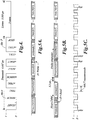
- FIGURE 4 and FIGURES 5A-5C are diagrams showing certain aspects of one implementation of a serial communication scheme for use with the electronic circuitry of FIGURE 3 .
- a compact touch probe is configured to input and output differential digital signals through the first and second electrical connections EC1 and EC2 (see FIGURE 3 ), which also carry DC power. It will be appreciated that, in addition to the requirement to transmit the touch probe trigger signals through the first and second electrical connections, it may be desirable to transmit and receive other data and/or commands between the touch probe and the host CMM through the first and second electrical connections.
- One implementation that provides all these features may be conveniently described as using two "signal modes".
- the differential digital signals may comprise control and data signals that are input and output superimposed on the connected supply voltage during control and data time periods
- the differential digital signals may comprise touch trigger signals generated by a trigger signal generating circuit (e.g., the trigger signal generating circuit 590) that are output superimposed on the connected supply voltage during trigger signal time periods that are different than the communication time periods.
- a trigger signal generating circuit e.g., the trigger signal generating circuit 590
- FIGURE 4 shows one exemplary "Normal mode" serial communication protocol that may be used to transmit touch trigger signals (as well as other information) from the touch probe to the host CMM at a desired probe sample cycle rate, which in some implementations is desirably at least 50,000 samples per second during ongoing touch probe measurement operations. In the illustrated implementation, it is 100,000 samples per second during ongoing touch probe measurement operations.
- a 10 microsecond "sample period” is divided into two parts, one 6.667 microsecond transmission sub-period “Transmit” (from probe), and one 3.333 microsecond listening sub-period “Listen”, where the host controller can initiate a transmission (to the probe), but normally does nothing during ongoing measurement operations.
- the signal DRIVE (see FIGURE 3 ) is controlled to put the differential signal configuration 560 in Transmit mode, and the communication processing circuit 550 outputs signals according to a protocol outlined below.
- the signal DRIVE (see FIGURE 3 ) is controlled to put the differential signal configuration 560 in Receive mode, and the communication processing circuit 550 receives signals according to a protocol outlined below.
- this protocol is repetitively streaming four bits of information; the TRIG, HALT, and COLL "trigger" signals and the Error flag, during the "Transmit” sub-period, as described in greater detail below.
- the complementary bits nTRIG, nHALT, and nCOLL are used so that there are always balanced numbers of '0' and '1' (five each) in this protocol. This allows the DC level of the AC coupled differential digital signals to maintain an average value, such that a varying DC signal component does not arise to leak through the AC coupling and reduce the safety margin for detecting the digital signal information.
- the three trigger signals, the TRIG, HALT, and COLL bits are indicative of three different displacement thresholds (e.g., as determined in the trigger threshold processing circuit 592, shown in FIGURE 3 ).
- each of the TRIG, HALT and COLL bits are zero or low, which is a "null" trigger signal generated when that the stylus displacement signal indicates that the stylus has not been deflected, and is therefore not in contact with a workpiece surface.
- the TRIG bit may be regarded as the "conventional" touch trigger signal, which indicates whether the stylus displacement signal currently exceeds the smallest (most sensitive) stylus displacement signal threshold.
- the host CMM may latch its current position values as a measurement of the touch point coordinates, according to known methods.
- the HALT bit may be used in some embodiments to assist in control of the host CMM, which may move or "overtravel" beyond the point where the stylus displacement signal corresponds to first touching the workpiece (e.g., as indicated by the TRIG bit), in order to more reliably ensure or confirm a valid touch measurement of the workpiece.
- the HALT bit indicates whether the stylus displacement signal currently exceeds a stylus displacement signal threshold corresponding to desired stopping point for the "confirming overtravel" of the CMM, beyond the point where the TRIG bit indicates a touch of the workpiece.
- the CMM motion may be stopped, and various measurement validation operations performed if desired, according to known methods.
- the COLL bit may be used in some embodiments to assist in control of the host CMM, in order to more reliably stop the CMM and minimize potential damage in the case of a "collision" of the stylus with an unexpected object or surface (e.g., an unanticipated fixture on the CMM, or the like).
- the COLL bit indicates whether the stylus displacement signal currently exceeds a "dangerous" threshold which is not expected to be encountered during normal CMM and/or touch probe operations.
- the CMM may implement an emergency stop, according to known methods.
- the Error flag bit may set to 1 or "high” upon the detection of various error conditions in the touch probe (e.g., in the electronic circuitry 500), according to known methods.
- the protocol shown in FIGURE 4 includes repetitively listening during the "Listen" sub-period (e.g., with the differential signal configuration 560 in Receive mode as outlined above.) If the host CMM initiates a transmission during the Listen sub-period, then the probe protocol changes to Command mode. In Command mode the host CMM can read and write to registers in the probe electronics circuitry 500 (e.g., to registers in the probe memory portion 580), for example for changing the trigger signal threshold levels or enabling filters, or the like. The host CMM may start transmitting the Preamble (described in greater detail below) during the Listen sub-period. The probe electronics circuitry 500 is configured to detect this and enters Command mode. During Command mode the probe suspends the Normal mode protocol outlined above (that is, transmission of trigger signal information is discontinued, etc.).
- Command mode the host controller sends read- and write-commands to the probe electronic circuitry registers.
- all Command mode data are transmitted in 8-bit binary form, LSB first, framed by a start bit and a stop bit.
- a DC-balanced encoding scheme such as the known Manchester encoding scheme, or the like
- this allows the DC level of the AC coupled differential digital signals to maintain an average value, such that a varying DC signal component does not arise to leak through the AC coupling and reduce the safety margin for detecting the digital signal information.
- FIGURES 5A and 5B show one exemplary "Command mode" implementation of a Write Sequence protocol (for host CMM writing to the touch probe) and a Read Sequence protocol (for host CMM reading from the touch probe), respectively.
- a DC-balanced encoding scheme is not illustrated, but it will be understood that the illustrated bytes may be transmitted using the application of Manchester encoding or the like, according to known methods, for reasons outlined above.
- the host CMM all bytes are written by the host CMM.
- the first two bytes are the Preamble for synchronization.
- the Preamble is only sent once as long as the transmit/receive direction remains the same, even when more than one command is sent.
- the Preamble is described further below with reference to FIGURE 5C .
- the third byte is the command code -- where bit seven specifies the Write command, '1', and Nbytes[0:6] specifies the number of data bytes that will follow the address.
- the maximum value of Nbytes is 127. For example, to write two bytes the command code is 82 16 .
- the fourth byte specifies the address at which the data bytes will be written.
- the maximum value of the address may be 255 in this implementation.
- the probe electronic circuitry's internal address register (e.g., as implemented in the operating memory manager 521) may be configured to increment after each byte is written. The fifth byte is the first data byte. There are N data bytes as specified by Nbytes. The probe electronic circuitry may copy the data bytes into its registers starting at the specified register address. After the last data byte, DataN, the probe expects another command from the host CMM. The host CMM should send the command without delay to maintain synchronization.
- FIGURE 5B As previously indicated, in this Command mode implementation, the two-byte Preamble shown in FIGURE 5A (and described further with reference to FIGURE 5C ) is only sent once as long as the transmit/receive direction remains the same, even when more than one command is sent.
- FIGURE 5B assumes that its Read Sequence is not the first command in Command mode -- otherwise, the two-byte Preamble would be required in addition to the illustrated bytes. Under these assumptions, in FIGURE 5B the host CMM writes the first two bytes and the probe electronics circuitry responds with the illustrated "probe response" bytes.
- the probe electronic circuitry responds by sending two Preamble bytes (see FIGURE 5C , below), then N bytes starting at the specified address, incrementing the address for each byte.
- the touch probe signal processing associated with generating the trigger signals may be continued in the probe electronic circuitry at the same probe sample cycle as during the Normal mode.
- trigger signal data may sent in the Normal mode according to the next "scheduled" data transmission time in the associated ongoing probe sample cycle.
- FIGURE 5C shows one exemplary "Command mode" implementation of the two-byte Preamble referred to above.
- the Preamble is illustrated including DC-balanced Manchester encoding.
- Manchester encoding recovers the clock signal with each data bit and is therefore robust even for long data sequences.
- DC-balanced Manchester encoding, or the like may also maximize the noise safety margin for detecting the AC coupled differential digital communications signals.
- Manchester encoding is applied (e.g., in the communication processing circuit 550) between the normal UART signals (e.g., in a portion of the digital communication circuit 540) and the signal lines TXD and RXD.
- the illustrated two-byte preamble serves to synchronize the transceiver receiver and transmitter that are communicating between the host CMM and the probe electronic circuitry.
- the transmitter sends the Preamble code 55 16 , D5 16 . Transmitting the LSB first, this code results in the timing diagram of Figure 5C .
- the Preamble has the useful feature that, in the first 18 bits, transitions occur only in the middle of the bit-time and not at the bit boundaries (vertical dashed lines.) This makes it easy to synchronize the receiver with the transmitter.
- the last three bits, '111', signal the end of the Preamble, and the circuitry connected to the receiver is configured to recognize these bits and implement an appropriate "ready state" in order to receive a command or data byte next.
- certain settings for the trigger threshold processing circuit 592, and/or other components or portions of the electronic circuitry 500 may be stored in the probe memory portion 580, such as may be accessed when a powered operating period is first started for the touch probe.
- a user may operate the host CMM to use the Command mode (e.g., by a user) to provide different thresholds, and/or low pass digital filter settings, etc., to be used by the trigger threshold processing circuit 592.
- such data may be stored in the CMM host system and may be provided each time a new powered operating period is started, and may override any default settings that are stored in the touch probe memory portion 580.
- any appropriate data/settings stored in the touch probe may be communicated to the second host CMM using the various protocols outlined above, to insure compatible operation with the second CMM host system.
Landscapes
- Physics & Mathematics (AREA)
- General Physics & Mathematics (AREA)
- A Measuring Device Byusing Mechanical Method (AREA)
- Measurement Of Length, Angles, Or The Like Using Electric Or Magnetic Means (AREA)
Abstract
Description
- This disclosure relates to precision metrology, and more particularly to touch probes used in coordinate measurement systems.
- Certain coordinate measurement systems, e.g., one-dimensional or three-dimensional measurement systems, such as coordinate measuring machines (CMMs), may obtain measurements of a workpiece using a touch probe configured to detect when a stylus of the touch probe contacts a workpiece. Touch probes use various types of displacement sensors to sense deflection of the touch probe stylus for an indication that it has contacted a workpiece.
- An exemplary prior art CMM utilizing a touch probe is described in
U.S. Patent No. 5,526,576 (the '576 patent), which is hereby incorporated herein by reference in its entirety. The '576 patent discloses a movement mechanism comprising multiple drives for moving the touch probe, an associated electronic system including a CANBUS digital communication system or the like, and features related to processing signals in (or from) the touch probe. A mechanical contact touch probe including two-way communication between the probe in a host machine, using only two wires, is described inU.S. Patent No. 4,817,362 (the '362 patent), which is hereby incorporated herein by reference in its entirety. In the 362 patent, touching a workpiece causes current changes in an electrical circuit within the probe, which is sensed by a current sensing circuit on the host machine. Communication from the machine to the probe is achieved by varying the voltage supplied to the probe, and initiating different functions in the probe based on the sensed supply voltage. - Another exemplary touch probe is disclosed in
U.S. Patent No. 5,755,038 (the '038 patent), which is hereby incorporated herein by reference in its entirety. The '038 patent discloses a compact touch probe that includes three strain gauges that are responsive to the probe's stylus deflection, and an ASIC processor that receives the strain gauge signals and generates an "auto-zeroed" trigger signal that is output to a host machine through a coaxial electrical connector. - While the systems disclosed in the disclosed in the '576, '362, and '038 patents include features related to processing signals in the touch probes, and/or communicating certain types of operating parameters and/or data using a limited number of wires between the touch probe and a host machine, in practice such features have been accompanied by undesirable tradeoffs. Adversely affected factors have included probe size, and/or the number of wires to the touch probe, and/or the related "retrofit ability" for use or compatibility with existing host machine hardware. Other compromised factors include the limited robustness and scope of the signals that are communicated, and/or ease of use, and the like. Improved systems and features which enable touch probes to communicate additional operating data without adding undesirable tradeoffs (e.g., while maintaining a minimum size, ease of use, and retrofit ability) would be desirable.
- This summary is provided to introduce a selection of concepts in a simplified form that are further described below in the Detailed Description. This summary is not intended to identify key features of the claimed subject matter, nor is it intended to be used as an aid in determining the scope of the claimed subject matter.
- Prior art touch probe configurations, including those indicated above, have been determined to have various undesirable combinations of features. The performance levels and miniaturization currently demanded in touch probe bodies has typically forced tradeoffs between all elements combined in such devices, particularly when adding a new feature or capability. For example, increased signal processing internal to a touch probe, and/or increased communication complexity between a touch probe and a host machine, has generally contributed to increased size, an increased number of wires to the touch probe, and/or limited "retrofit ability" for using the touch probe with existing host machine hardware. One factor hindering improved solutions to these problems has been that it has proved difficult to provide configurations that achieve similar high accuracy measurements (e.g., micron or submicron level repeatability), internal signal processing, and digital signal communication with external devices, in a compact configuration (e.g., on the order of 12-15 millimeter diameter in some implementations, or about the size of a human "pinky" finger).
- In contrast to the prior art, disclosed herein is a configuration for a touch probe that includes a unique combination of features which allows useful digital signal processing and control functions in a touch probe, as well as reliable trigger signal transmission and two-way digital signal communication with a host CMM, without the need for an associated size increase, and using only two electrical connections between the touch probe and the host CMM. By way of example, and not by way of limitation, such a configuration may allow increased probe functionality and/or ease-of-use, as well as a "retrofit ability" for using the touch probe with existing host machine hardware.
- In accordance with various principles disclosed herein, a compact touch probe including internal digital signal processing is provided, for use with a CMM. The compact touch probe comprises: a displacement sensor configured to output at least one sensor signal that is responsive to displacement of a stylus attached to the touch probe; an interface connector including first and second electrical connections that electrically connect the touch probe to the CMM; and touch probe electronic circuitry, included entirely within a housing of the compact touch probe.
- The touch probe electronic circuitry comprises a regulated power supply circuit; probe operating circuits and memory; a trigger signal generating circuit that inputs the at least one sensor signal and generates a touch trigger signal corresponding to a displacement of the stylus; and a digital communication circuit including a differential signal configuration that inputs and outputs differential digital signals through the first and second electrical connections. The touch probe electronic circuitry further comprises a specialized supply isolation configuration that is coupled to the first and second electrical connections to receive a connected supply voltage from the CMM through the first and second electrical connections, and is configured to isolate the regulated power supply circuit from loading the differential digital signals that pass through the first and second electrical connections.
- In various implementations, the specialized supply isolation configuration comprises: a first end of a first winding of a differential mode choke coupled to the first electrical connection, with a second end of the first winding of the differential mode choke connected to a positive input of the regulated power supply circuit; a first end of a second winding of the differential mode choke coupled to the second electrical connection, with a second end of the second winding of the differential mode choke connected to a negative input (e.g., a circuit ground connection) of the regulated power supply circuit; and at least a first supply isolation capacitor coupled between the positive and negative inputs of the regulated power supply circuit. The specialized supply isolation is configured in combination with other operating characteristics of the touch probe electronics in order to achieve the desirable touch probe characteristics outlined above, without significant compromise. In various implementations, the differential mode choke operating impedance may be significantly smaller (e.g., up to 1000 times smaller) in comparison to known isolation designs used in other type of applications.
- In various implementations, the digital communication circuit comprises a differential signal configuration that is AC coupled to the first and second electrical connections through a communication isolation configuration comprising a first capacitor coupled in series to the first electrical connection and a second capacitor coupled in series to the second electrical connection, and the differential signal configuration is configured to input and output the differential digital signals through the first and second electrical connections. In various implementations, the differential digital signals comprise control and data signals that are input and output superimposed on the connected supply voltage during control and data time periods, and touch trigger signals generated by the trigger signal generating circuit that are output superimposed on the connected supply voltage during trigger signal time periods that are different than the control and data time periods. In various embodiments, at least a majority of the differential digital signals are formatted based on a serial communication code scheme that is nominally DC-balanced.
-
-
FIGURE 1 is a diagram showing various components of a measuring system including a CMM utilizing a touch probe such as that disclosed herein; -
FIGURE 2 is a diagram showing a perspective view of an implementation of a touch probe; -
FIGURE 3 is a partially schematic block diagram showing one implementation of electronic circuitry for a touch probe including touch probe digital serial communication superimposed on two touch probe power supply lines; and -
FIGURES 4 and 5A-5C are diagrams showing certain aspects of one implementation of a serial communication scheme for use with the electronic circuitry ofFIGURE 3 . -
FIGURE 1 is a diagram showing various components of ameasuring system 100 including a CMM 100' utilizing a touch probe 200' such as that disclosed herein. Coordinate measuring machines (CMMs) are known in the art, for example, in U.S. Pat. Appl. Publ. No.2011/0192044, to Usui , which is hereby incorporated by reference in its entirety. An arrangement of a CMM is illustrated schematically inFIGURE 1 , showing ameasuring system 100 including a CMM 100', which uses a touch probe 200'. The touch probe 200' may include aprobe body 200. Themeasuring system 100 includes anoperating unit 10, amotion controller 15 that controls movements of the CMM 100', ahost computer 20 and the CMM 100'. Theoperating unit 10 is coupled to themotion controller 15 and may includejoysticks 11 for manually operating the CMM 100'. Thehost computer 20 is coupled to themotion controller 15 and operates the CMM 100' and processes measurement data for a workpiece W according to known methods. Thehost computer 20 includes input means 25 (e.g., a keyboard, etc.) for inputting, for example, measurement conditions, and output means 30 (e.g., a display, printer, etc.) for outputting, for example, measurement results. - The CMM 100' includes a
drive mechanism 120 which is located on asurface plate 110, and anattachment portion 124 for attaching the touch probe 200' to thedrive mechanism 120. Thedrive mechanism 120 includes x-axis, y-axis, and z-axis slide mechanisms stylus 164 attached to the touch probe 200' includes acontact portion 165. Astylus module 160 may attach thestylus 164 to a stylus suspension portion of theprobe body 200, which allows thestylus 164 to deflect when its contact portion 165 (e.g., a ruby sphere) contacts the surface of the workpiece W, to produce a touch trigger signal. The characteristics and operations of commercially available CMMs are generally known in the art, and are therefore not described in greater detail herein. - The touch probe 200' provides a 3-D tactile probing system having characteristics such as general mechanical stiffness and signal sensitivity to the deflection of the
stylus 164, so that the characteristics can be reliably trusted to properly reflect the actual coordinates measured by the probing system, with repeatability at the submicron level. For economical high throughput, it may be generally desirable to perform all operations (e.g., motions and sensing) of the CMM 100' at high speed. An exemplary implementation of a high speed contact detector is disclosed in US Pat. Appl. Publ. No.2015/0323300, to Briegel et al. , which is hereby incorporated herein by reference in its entirety. -
FIGURE 2 is a diagram showing a perspective view of an implementation of a touch probe 200' including aprobe body 200. As shown inFIGURE 2 , theprobe body 200 includes ahousing 301 shown in phantom to reveal a circuitboard assembly configuration 400 and a moving element assembly 300 disposed in thehousing 301. Theprobe body 200 in this implementation includes thehousing 301, aconnection assembly 302 configured for mechanically and electrically connecting theprobe body 200 to a measuring system such as a CMM (e.g., the CMM shown inFIGURE 1 ); a rigidprobe body structure 310, a circuitboard assembly configuration 400, and a moving element assembly 300 comprising a compliantelement mounting frame 320, a stylus suspension portion 340 (hidden) and a displacement sensing configuration 350 (hidden). - In the illustrated implementation, the
connection assembly 302 rigidly connects theprobe body 200 and its circuitry to a CMM. Theconnection assembly 302 includes a threaded connection/connector 304 which is a mounting and electrical connection and a contact electrical connection/connector 303, which are electrically isolated from one another by aninsulator 306. Theconnection assembly 302 is fixed relative to thehousing 301. In one embodiment, the connection/connector 304 may include a flange portion (hidden inside an annularhousing cap portion 305 inFIGURE 2 ) that is fixed by compression between thehousing 301 and the annularhousing cap portion 305. In various embodiments the flange portion may be compressed through a surrounding insulator or insulators (e.g., the insulator 308) such that it is electrically isolated from thehousing 301 and annularhousing cap portion 305. It may be appreciated that theconnection assembly 302 includes only two electrical connections, and is functionally similar to a known "legacy" type of touch probe mounting connector, used primarily with analog type touch probe signals. Therefore, the touch probe 200' may used with existing CMM mounting interface hardware, which may include expensive motorized joints and the like. A similar connector assembly is illustrated inFigure 1 of the incorporated '038 patent, for example. It should be appreciated that theconnection assembly 302 is exemplary interface connector only, and not limiting. In various embodiments, an interface connector have two electrical connections may be provided separately from a mechanical mounting arrangement. Though not as elegant as theconnection assembly 302, such an arrangement may still be useful in certain retrofit applications, if desired. -
FIGURE 2 further illustrates astylus module 160 which rigidly holds astylus 164 and attaches to a movablestylus capture element 343D included in movingassembly 343 of theprobe body 200, which is coupled to the moving element assembly 300. This allows thestylus 164 to deflect when itscontact portion 165 contacts the surface of a workpiece, to produce a trigger signal. The compliantelement mounting frame 320 is joined to, and forms an additional part of, the rigidprobe body structure 310. The compliantelement mounting frame 320 includes acentral portion 320A, anupper portion 320B and alower portion 320C, which are clamped together by screws in this implementation. Various compliant and/or moving elements and associated sensing elements are assembled inside the compliantelement mounting frame 320, to form the moving element assembly 300. - In one implementation, an axial extension portion 330 (not shown) includes an axial member that has a triangular cross section that is sized to receive the circuit
board assembly configuration 400 with the component mounting portions 402A (not visible), 402B, 402C, which may be interconnected by a flexible circuit member (layer) 403, generally aligned to overlie a face of the axial extension portion 330. The circuitboard assembly configuration 400 is securely disposed and supported within thehousing 301, between an upper mounting portion of theconnection assembly 302 and the main body of the moving element assembly 300. Aflexible conductor connector 351 may connect signals from the displacement sensors of the displacement sensing configuration 350 to the circuitboard assembly configuration 400. The illustrated implementation is exemplary only, and not limiting. - In various implementations, the touch probe 200' is desirably relatively compact and lightweight (e.g., on the order of 12-15 millimeter diameter in some implementations), to facilitate rapid accelerations/decelerations and minimize vibration, all of which contribute to higher precision CMM inspection throughput. It should be appreciated that a compact size and light weight also generally restrict the size and complexity of the internal circuitry. In some implementations, to conserve space and power consumption while providing increased capabilities and processing in the touch probe 200', a commercially available field programmable gate array (FPGA) is included on the circuit
board assembly configuration 400, and configured to provide useful or essential functions such as trigger signal processing, serial communications, and certain memory functions using built-in capabilities of the FPGA. The circuitboard assembly configuration 400 illustrates a corresponding circuit layout. This provides a "smart" compact touch probe that provides increased functionality, versatility, and ease of use in comparison to a variety of known compact touch probes. However, the advantages of combining such internal processing features with a compact touch probe configuration may not be accepted, if problems associated with the limitation of using only two electrical connections between the touch probe and the host CMM are not overcome (e.g., to provide the legacy CMM interface compatibility advantage outlined previously). Solution(s) to various aspects of this two connection (or "two wire") touch probe interface problem are disclosed herein, as described in greater detail below. - The two wire interface generally requires that power and communication signals are superimposed on the same wires. Doing so is generally known of one skilled in the art of electronic system design, and numerous examples of doing so may be found on the Internet. In addition to some of the incorporated references,
US Patents No. 7,689,176 ,5,644,286 ,5,210,519 , and5,859,584 , disclose various alternative systems related to superimposing power and communication signals on the same wires. However, all of these patents require undesirable compromises in terms of requiring wireless data transmission, or extra electrical connections, or limited communication signal content, or incompatible circuit or component sizes, in relation to using their disclosed principles in a compact "smart" touch probe. One aspect of the two wire interface problem is represented inFIGURE 2 in the illustration of the circuitboard assembly configuration 400, which shows that space on the circuit boards is limited, and furthermore that the allowed height of components inside thehousing 301 is limited. One way to isolate the power and communication signals is to employ a choke in a signal or supply isolation configuration. An approximate placement and chokevolume 471 is schematically represented in dashed outline. In general, thechoke volume 471, is inadequate for the straightforward use of standard or known isolation circuits in a compact touch probe. Instead, a unique combination of probe features, circuit characteristics, and communication signal features are required for providing reliable "two wire" operation of the compact touch probe 200', or the like, as disclosed in greater detail below. -
FIGURE 3 is a block diagram showing adisplacement sensor configuration 595, and various elements of one implementation ofelectronic circuitry 500 for a touch probe including digital serial communication superimposed on two power supply lines (e.g., as may be included in the circuitboard assembly configuration 400 ofFIGURE 2 ). In various implementations, a configuration of acompact probe body 200 such as that illustrated inFIGURE 2 allows corresponding components to be assembled in the circuit board assembly configuration 400 (e.g., in a compact diameter of 12-15 millimeters) to provide certain signal processing operations in the probe, for example corresponding to the following description, using economical non-custom components. Additional details regarding certain types of electronic circuitry for a touch probe that may perform some similar operations as theelectronic circuitry 500 may be found in commonly assignedUS Patent Applications No. 62/271,082 62/325,763 - In the implementation shown in
FIGURE 3 , theelectronic circuitry 500 includes a triggersignal generating circuit 590 connected to thedisplacement sensor configuration 595, probe operating circuits andmemory portion 510, a regulatedpower supply circuit 575, and asupply isolation configuration 570. In various embodiments, thedisplacement sensor configuration 595 may comprise at least one displacement sensor (e.g., 3 or 4 strain gauges, or more) and output at least one sensor signal (e.g., 3 or 4 sensor signals, or more) that is responsive to displacement of the stylus attached to the touch probe. The triggersignal generating circuit 590 may include a signalcombination processing portion 591 and a triggerthreshold processing circuit 592, and generate atouch trigger signal 597T corresponding to displacement of the stylus, as described in greater detail below. The probe operating circuits (and processing) andmemory portion 510 may includeprobe operating circuits 520 and aprobe memory portion 580. It will be appreciated that various circuits described herein may provide various signal processing and/or control operations according to embedded code, or routines or programs, or the like, as will be understood by one of ordinary skill in the art. Theprobe operating circuits 520 may include anoperating memory manager 521 and digital communication circuit(s) 540. Theprobe memory portion 580 may include anon-volatile memory portion 581, a probe operating routines andconfigurations memory portion 582, and a probe operatingparameters memory portion 583. In the illustrated embodiment, the digital communication circuit(s) 540 may include acommunication processing circuit 550, connected to an input/outputdifferential signal configuration 560 comprising a transmitter/receiver portion 561 and a driver integratedcircuit portion 562. In various embodiments, the elements of thedigital communication circuit 540 and/or the input/outputdifferential signal configuration 560 may be merged and/or indistinguishable. Thedigital communication circuit 540 is configured to input and output differential digital signals (comprising signal(s) DDS1 and DDS2) on the lines SL1 and SL2 through the first and second electrical connections EC1 and EC2, respectively. In the illustrated embodiment, the connections EC1 and EC2 are part of a connector MC (e.g., theconnection assembly 302, shown inFIGURE 2 .) Exemplary differential digital signals are described further below. - The regulated
power supply circuit 575 may be configured to provide one or more regulated voltages (e.g., the voltages V1out, V2out, V3out) to various portions of theelectronic circuitry 500, according to known techniques. In one embodiment, the regulatedpower supply circuit 575 may comprise one or more commercially available voltage regulator IC's outputting voltages of 1.2, 2.5 and 3.3 volts, for example. - In various embodiments, a
supply isolation configuration 570 may be used in the lines VL1 and VL2, such that it is coupled through the first and second electrical connections EC1 and EC2 to receive a connected supply voltage from the CMM (e.g., through the host lines HL1 and HL2, which may be connected to the first and second electrical connection EC1 and EC2). Thesupply isolation configuration 570 is configured to isolate the regulated power supply circuit from loading the differential digital signals DDS1 and DDS2 that pass through the first and second electrical connections EC1 and EC2. One exemplary embodiment of thesupply isolation configuration 570 is illustrated inFIGURE 3 , wherein: a first end of a first winding of adifferential mode choke 571 is coupled to the first electrical connection EC1, with a second end of the first winding of thedifferential mode choke 571 connected to a positive input of the regulatedpower supply circuit 575; a first end of a second winding of thedifferential mode choke 571 coupled to the second electrical connection EC2, with a second end of the second winding of the differential mode choke connected to a negative input of the regulated power supply circuit (e.g., the ground input Gnd); and, at least a firstsupply isolation capacitor 572 is coupled between the positive and negative inputs of the regulatedpower supply circuit 575. In one implementation, thesupply isolation capacitor 572 may have a value on the order of 45 µF (however, this value is exemplary only, and not limiting). In some embodiments, a plurality of parallel supply isolation capacitors may function as the supply isolation capacitor 572 (e.g., due to layout and/or size constraints.) A reversevoltage protection diode 573 may optionally be coupled between the positive and negative inputs of the regulatedpower supply circuit 575, as shown inFIGURE 3 . - In various implementations the characteristics of the
differential mode choke 571 are selected in combination with other operating characteristics of the touch probe electronics (e.g., the electronic circuitry 500), in order to provide reliable operation for a compact touch probe including digital serial communication superimposed on two power supply lines, without compromising the compactness of the touch probe. For example, in some implementations, thedifferential mode choke 571 may be selected to have an impedance on the order of 10-25 µH for frequencies associated with the differential digital signals DDS1 and DDS2 (although such an impedance is exemplary only, and not limiting, in various implementations.) This is an extremely small impedance, which may generally be considered too small for the intended function (e.g., by a factor of 1000), in various known applications. According to known principles, it might be thought that using a high frequency for the differential digital signals DDS1 and DDS2 could be useful for increasing the inductive impedance presented to them by thedifferential mode choke 571. However, in the implementations disclosed herein, in addition to isolating the differential digital signals DDS1 and DDS2 from being loaded by the power supply circuit, thedifferential mode choke 571 must freely pass DC voltage and/or current. The small impedance outlined above for thedifferential mode choke 571 allows a small component size, which is advantageous for packaging a compact touch probe, but it also leads to problems with DC current effects saturating the core of the differential mode choke 571 (thereby reducing its effectiveness). Thus, the DC current draw (and/or general power consumption) in a compact touch probe must be minimized in conjunction with using a smalldifferential mode choke 571. High digital signal frequencies may be associated with greater power consumption and/or DC current draw. Therefore, against known teachings, in various compact touch probe electronic implementations disclosed herein, a relatively low frequency digital signal processing and/or digital communication signals is desirably used in combination with a very smalldifferential mode choke 571. In some embodiments, the voltage from the host CMM received at the first and second electrical connection EC1 and EC2 may be approximately 4 volts, and the touch probeelectronic circuitry 500 may be configured to draw approximately 100mA, or 85 mA, or less, in some embodiments. The differential digital communication signals may have an operating frequency or bit rate on the order of 1.5Mbps in some implementations. Exemplary digital communication signals which may be used in combination with theelectronic circuitry 500 in a compact touch probe are described in greater detail below with reference forFIGURE 4 and FIGURES 5A-5C . It will be appreciated that the circuit operation and component values outlined above are exemplary only, and not limiting. Various adjustments to the various outlined combinations of characteristics outlined herein may be made, based on adaptations according to principles disclosed herein. -
FIGURE 3 also schematically shows an "unregulated" voltage VU being supplied to a portion of theelectronic circuitry 500, reducing the load and related losses in the regulatedpower supply circuit 575. In particular, the unregulated voltage VU may be used to power thedifferential signal configuration 560, which also allows the differential signal(s) DDS1 and DDS2 to have the highest possible differential voltage, to enhance their signal-to-noise (S/N) ratio. - In operation, the
displacement sensor configuration 595 is configured to output at least one sensor signal that is responsive to displacement of a stylus (e.g., the stylus 164) as attached to the touch probe. In various implementations, thedisplacement sensor configuration 595 may include various components and sensors (e.g., internal flexures, strain gauges, etc.) for sensing relatively small deflections of the touch probe stylus. The triggersignal generating circuit 590 may be implemented according to principles known to one skilled in the art of touch probe design and/or as disclosed in the incorporated references. In one exemplary implementation, the triggersignal generating circuit 590 may input a plurality of displacement signals (e.g., from various sensors included in thedisplacement sensor configuration 595, such as a configuration of four strain gauges, etc.) The signalcombination processing portion 591 receives the signals and determines a combined displacement signal (e.g., a displacement magnitude). The triggerthreshold processing circuit 592 defines a switching threshold value and compares it to the combined displacement signal. When the combined displacement signal exceeds the switching threshold value, the triggerthreshold processing circuit 592 outputs atouch trigger signal 597T indicating that the stylus has contacted a workpiece. A hysteresis circuit at the output may enhance the trigger signal stability using known methods. A further example of trigger signal determination circuits and processing methods, including switching threshold definition, is described inU.S. Patent No. 7,792,654 , which is hereby incorporated herein by reference in its entirety. In the illustrated embodiment, thetouch trigger signal 597T may be communicated to a host CMM, or the like, through thedigital communication circuit 540 or a portion thereof, as a differential digital signal on the lines SL1 and SL2 and through first and second electrical connections EC1 and EC2, during a trigger signal time period, as described in greater detail below. - In various embodiments, an "AC coupled" communication isolation configuration is used in the lines SL1 and SL2. One exemplary
communication isolation configuration 565 is illustrated inFIGURE 3 , wherein: a first communication isolation capacitor 566-1 is coupled in series to the first electrical connection EC1 and to a first transceiver node TN1 of thedifferential signal configuration 560, and a second communication isolation capacitor 566-2 is coupled in series between the second electrical connection EC2 and to a second transceiver node TN2 of thedifferential signal configuration 560. In the illustrated embodiment, the first and second communication capacitors 566-1 and 566-2 are coupled to respective transceiver nodes through acommon mode choke 567. However, in some embodiments, the signal reliability and/or noise may be sufficient without thecommon mode choke 567, and its use is optional. In such embodiments, first communication isolation capacitor 566-1 may be coupled in series directly from the first electrical connection EC1 to the first transceiver node TN1, and the second communication isolation capacitor 566-2 may be coupled in series directly from the second electrical connection EC2 to the second transceiver node TN2. The illustrated embodiment using the optionalcommon mode choke 567 may, in some applications (e.g., in "electrically noisy" systems or environments), provide enhanced signal reliability. In such embodiments, the first communication isolation capacitor 566-1 is coupled in series from the first electrical connection EC1 to a first end of a first winding of thecommon mode choke 567, and a second end of the first winding of thecommon mode choke 567 is coupled to a first transceiver node TN1. The second communication isolation capacitor 566-2 is coupled in series from the second electrical connection EC2 to a first end of a second winding of thecommon mode choke 567, and a second end of the second winding of thecommon mode choke 567 is coupled to the second transceiver node TN2. - In either of the configurations outlined above, it may be advantageous (but optional) to use a
termination resistor 568 coupled between the first and second transceiver nodes TN1 and TN2, with a value selected to match the impedance of the lines SL1 and SL2 according to known impedance matching principles. - In any of the "AC coupled" communication isolation configurations outlined above, the first and second communication isolation capacitors 566-1 and 566-2 pass the "AC" differential digital signal(s) on the lines SL1 and SL2, and block the DC voltage present at the first and second electrical connections EC1 and EC2 from reaching the
differential signal configuration 560. Thecommon mode choke 567, if used, blocks common mode signals (a type of noise) from reaching thedifferential signal configuration 560. In one embodiment, thechoke 567 may be relatively small physically and may be selected to provide an impedance on the order of 100 ohms at 100MHz, in order to suppress broadband noise. In one embodiment, the capacitors 566-1 and 566-2 may have a capacitance of approximately 1µF. However, these various values are exemplary only, and not limiting. - As previously outlined, in some embodiments, the
electronic circuitry 500 may include a commercially available field programmable gate array (FPGA), configured to provide useful or essential functions such as trigger signal processing, serial communications, and certain memory functions using built-in capabilities of the FPGA. In such implementations some of the probe operating circuits (and processing) 520 may be implemented in the FPGA, such as some or most of thedigital communications circuits 540, including thecommunication processing circuit 550. In any case, in various embodiments thecommunication processing circuit 550 may implement a digital communication protocol (e.g., a serial communication protocol). In the implementation illustrated inFIGURE 3 , thecommunication processing circuit 550 implements a serial communication protocol and interacts with and/or controls thedifferential signal configuration 560 over the signal lines RXD, TXD, and DRIVE. In one implementation, thedifferential signal configuration 560 may comprise suitable commercially available RS485 transceiver IC's, which are widely available and known to one of ordinary skill in the art, and the signal lines RXD, TXD, and DRIVE are compatible with such transceiver IC's, if desired. - In the illustrated implementation, the line RXD carries serial data received at the transceiver nodes TN1 and TN2 as differential signals from the host CMM. The line TXD carries serial data to be transmitted at the transceiver nodes TN1 and TN2 as differential signals from the touch probe to the host CMM. The line DRIVE is connected to "enable" pins or inputs of the
differential signal configuration 560. At any given time, thedifferential signal configuration 560 can either transmit or receive, but not both simultaneously. A first polarity digital signal on the line DRIVE enables receiving differential digital signals from the host CMM, and the opposite polarity digital signal on the line DRIVE enables transmitting differential digital signals to the host CMM. One exemplary serial communication protocol which may be used in combination with features outlined above is described in greater detail below. -
FIGURE 4 and FIGURES 5A-5C are diagrams showing certain aspects of one implementation of a serial communication scheme for use with the electronic circuitry ofFIGURE 3 . As previously outlined, in various embodiments disclosed herein a compact touch probe is configured to input and output differential digital signals through the first and second electrical connections EC1 and EC2 (seeFIGURE 3 ), which also carry DC power. It will be appreciated that, in addition to the requirement to transmit the touch probe trigger signals through the first and second electrical connections, it may be desirable to transmit and receive other data and/or commands between the touch probe and the host CMM through the first and second electrical connections. One implementation that provides all these features may be conveniently described as using two "signal modes". For example, in a "Command mode" the differential digital signals may comprise control and data signals that are input and output superimposed on the connected supply voltage during control and data time periods, and in a "Normal mode" the differential digital signals may comprise touch trigger signals generated by a trigger signal generating circuit (e.g., the trigger signal generating circuit 590) that are output superimposed on the connected supply voltage during trigger signal time periods that are different than the communication time periods. -
FIGURE 4 shows one exemplary "Normal mode" serial communication protocol that may be used to transmit touch trigger signals (as well as other information) from the touch probe to the host CMM at a desired probe sample cycle rate, which in some implementations is desirably at least 50,000 samples per second during ongoing touch probe measurement operations. In the illustrated implementation, it is 100,000 samples per second during ongoing touch probe measurement operations. In the example shown inFIGURE 4 , a 10 microsecond "sample period" is divided into two parts, one 6.667 microsecond transmission sub-period "Transmit" (from probe), and one 3.333 microsecond listening sub-period "Listen", where the host controller can initiate a transmission (to the probe), but normally does nothing during ongoing measurement operations. For example, in one implementation, during the Transmit sub-period the signal DRIVE (seeFIGURE 3 ) is controlled to put thedifferential signal configuration 560 in Transmit mode, and thecommunication processing circuit 550 outputs signals according to a protocol outlined below. Conversely, during the Listen sub-period the signal DRIVE (seeFIGURE 3 ) is controlled to put thedifferential signal configuration 560 in Receive mode, and thecommunication processing circuit 550 receives signals according to a protocol outlined below. - In the illustrated implementation, this protocol is repetitively streaming four bits of information; the TRIG, HALT, and COLL "trigger" signals and the Error flag, during the "Transmit" sub-period, as described in greater detail below. The complementary bits nTRIG, nHALT, and nCOLL are used so that there are always balanced numbers of '0' and '1' (five each) in this protocol. This allows the DC level of the AC coupled differential digital signals to maintain an average value, such that a varying DC signal component does not arise to leak through the AC coupling and reduce the safety margin for detecting the digital signal information. The bit rate in this example is 15 bits per 10 µs = 1.5 Mbps.
- In this example, the three trigger signals, the TRIG, HALT, and COLL bits, are indicative of three different displacement thresholds (e.g., as determined in the trigger
threshold processing circuit 592, shown inFIGURE 3 ). In the illustrated example, each of the TRIG, HALT and COLL bits are zero or low, which is a "null" trigger signal generated when that the stylus displacement signal indicates that the stylus has not been deflected, and is therefore not in contact with a workpiece surface. The TRIG bit may be regarded as the "conventional" touch trigger signal, which indicates whether the stylus displacement signal currently exceeds the smallest (most sensitive) stylus displacement signal threshold. In response to the TRIG bit indicating the stylus is touching the workpiece (TRIG bit equals 1, or "high"), the host CMM may latch its current position values as a measurement of the touch point coordinates, according to known methods. The HALT bit may be used in some embodiments to assist in control of the host CMM, which may move or "overtravel" beyond the point where the stylus displacement signal corresponds to first touching the workpiece (e.g., as indicated by the TRIG bit), in order to more reliably ensure or confirm a valid touch measurement of the workpiece. The HALT bit indicates whether the stylus displacement signal currently exceeds a stylus displacement signal threshold corresponding to desired stopping point for the "confirming overtravel" of the CMM, beyond the point where the TRIG bit indicates a touch of the workpiece. In response to the HALT bit indicating a desired stopping point for "overtravel" of the CMM (HALT bit equals 1, or "high"), the CMM motion may be stopped, and various measurement validation operations performed if desired, according to known methods. The COLL bit may be used in some embodiments to assist in control of the host CMM, in order to more reliably stop the CMM and minimize potential damage in the case of a "collision" of the stylus with an unexpected object or surface (e.g., an unanticipated fixture on the CMM, or the like). The COLL bit indicates whether the stylus displacement signal currently exceeds a "dangerous" threshold which is not expected to be encountered during normal CMM and/or touch probe operations. In response to the COLL bit indicating an unexpected stylus deflection (COLL bit equals 1, or "high"), the CMM may implement an emergency stop, according to known methods. The Error flag bit may set to 1 or "high" upon the detection of various error conditions in the touch probe (e.g., in the electronic circuitry 500), according to known methods. - The protocol shown in
FIGURE 4 includes repetitively listening during the "Listen" sub-period (e.g., with thedifferential signal configuration 560 in Receive mode as outlined above.) If the host CMM initiates a transmission during the Listen sub-period, then the probe protocol changes to Command mode. In Command mode the host CMM can read and write to registers in the probe electronics circuitry 500 (e.g., to registers in the probe memory portion 580), for example for changing the trigger signal threshold levels or enabling filters, or the like. The host CMM may start transmitting the Preamble (described in greater detail below) during the Listen sub-period. Theprobe electronics circuitry 500 is configured to detect this and enters Command mode. During Command mode the probe suspends the Normal mode protocol outlined above (that is, transmission of trigger signal information is discontinued, etc.). - In Command mode the host controller sends read- and write-commands to the probe electronic circuitry registers. In one exemplary implementation, all Command mode data are transmitted in 8-bit binary form, LSB first, framed by a start bit and a stop bit. In various implementations of the Command mode protocol, it may be desirable to use a DC-balanced encoding scheme (such as the known Manchester encoding scheme, or the like) in the touch probe electronic circuitry (e.g., in the communication processing circuit 550) and the host CMM. In a manner similar to that previously outlined with reference to DC-balance protocol shown in
FIGURE 4 , this allows the DC level of the AC coupled differential digital signals to maintain an average value, such that a varying DC signal component does not arise to leak through the AC coupling and reduce the safety margin for detecting the digital signal information. -
FIGURES 5A and 5B , show one exemplary "Command mode" implementation of a Write Sequence protocol (for host CMM writing to the touch probe) and a Read Sequence protocol (for host CMM reading from the touch probe), respectively. For clarity of description and compactness of illustration, a DC-balanced encoding scheme is not illustrated, but it will be understood that the illustrated bytes may be transmitted using the application of Manchester encoding or the like, according to known methods, for reasons outlined above. - In
FIGURE 5A , all bytes are written by the host CMM. The first two bytes are the Preamble for synchronization. In this implementation, the Preamble is only sent once as long as the transmit/receive direction remains the same, even when more than one command is sent. The Preamble is described further below with reference toFIGURE 5C . In this implementation, the third byte is the command code -- where bit seven specifies the Write command, '1', and Nbytes[0:6] specifies the number of data bytes that will follow the address. The maximum value of Nbytes is 127. For example, to write two bytes the command code is 8216. The fourth byte specifies the address at which the data bytes will be written. The maximum value of the address may be 255 in this implementation. The probe electronic circuitry's internal address register (e.g., as implemented in the operating memory manager 521) may be configured to increment after each byte is written. The fifth byte is the first data byte. There are N data bytes as specified by Nbytes. The probe electronic circuitry may copy the data bytes into its registers starting at the specified register address. After the last data byte, DataN, the probe expects another command from the host CMM. The host CMM should send the command without delay to maintain synchronization. - With regard to
FIGURE 5B , as previously indicated, in this Command mode implementation, the two-byte Preamble shown inFIGURE 5A (and described further with reference toFIGURE 5C ) is only sent once as long as the transmit/receive direction remains the same, even when more than one command is sent.FIGURE 5B assumes that its Read Sequence is not the first command in Command mode -- otherwise, the two-byte Preamble would be required in addition to the illustrated bytes. Under these assumptions, inFIGURE 5B the host CMM writes the first two bytes and the probe electronics circuitry responds with the illustrated "probe response" bytes. There is a short delay illustrated between the host CMM transmission of the first two bytes, and the probe response transmission of the probe response bytes, allowing the differential signal configuration in the touch probe (e.g., seeelement 560 inFIGURE 3 ) as well as its counterpart in the host CMM to change the direction of their transceivers. In the illustrated example, this delay is approximately 5.3µs. After this delay, the probe electronic circuitry responds by sending two Preamble bytes (seeFIGURE 5C , below), then N bytes starting at the specified address, incrementing the address for each byte. After a Read Sequence protocol ends, in the illustrated implementation the probe electronic circuitry may automatically terminate Command mode and resume the previously outlined Normal mode, by default. (In one implementation, Command mode may be ended under any circumstances by the host CMM sending a Read or Write Sequence, with Nbytes = 0. No address or data is needed.) - In various implementations, during the Command mode, the touch probe signal processing associated with generating the trigger signals may be continued in the probe electronic circuitry at the same probe sample cycle as during the Normal mode. In such implementations, when Command mode ends and the Normal mode is resumed, trigger signal data may sent in the Normal mode according to the next "scheduled" data transmission time in the associated ongoing probe sample cycle.
-
FIGURE 5C shows one exemplary "Command mode" implementation of the two-byte Preamble referred to above. In the illustrated example, the Preamble is illustrated including DC-balanced Manchester encoding. As is known, Manchester encoding recovers the clock signal with each data bit and is therefore robust even for long data sequences. As previously indicated, DC-balanced Manchester encoding, or the like, may also maximize the noise safety margin for detecting the AC coupled differential digital communications signals. In the illustrated example it is assumed that Manchester encoding is applied (e.g., in the communication processing circuit 550) between the normal UART signals (e.g., in a portion of the digital communication circuit 540) and the signal lines TXD and RXD. This means that both the start bit and the stop bit are retained in the illustrated communication frames. The illustrated example assumes the application of the phase convention of IEEE 802.3 (Ethernet) where a high-to-low transition represents '0', and a low-to-high transition represents '1'. - The illustrated two-byte preamble serves to synchronize the transceiver receiver and transmitter that are communicating between the host CMM and the probe electronic circuitry. In the illustrated example, the transmitter sends the Preamble code 5516, D516. Transmitting the LSB first, this code results in the timing diagram of
Figure 5C . The Preamble has the useful feature that, in the first 18 bits, transitions occur only in the middle of the bit-time and not at the bit boundaries (vertical dashed lines.) This makes it easy to synchronize the receiver with the transmitter. The last three bits, '111', signal the end of the Preamble, and the circuitry connected to the receiver is configured to recognize these bits and implement an appropriate "ready state" in order to receive a command or data byte next. - With regard to some examples of use of the Command mode, certain settings (e.g., default settings) for the trigger
threshold processing circuit 592, and/or other components or portions of theelectronic circuitry 500 may be stored in theprobe memory portion 580, such as may be accessed when a powered operating period is first started for the touch probe. However, if it is determined that the default thresholds for the triggerthreshold processing circuit 592 are not producing the desired results in a particular environment and/or application (e.g., too many false trigger signals, etc.), a user may operate the host CMM to use the Command mode (e.g., by a user) to provide different thresholds, and/or low pass digital filter settings, etc., to be used by the triggerthreshold processing circuit 592. In some implementations, such data may be stored in the CMM host system and may be provided each time a new powered operating period is started, and may override any default settings that are stored in the touchprobe memory portion 580. In certain implementations, if the touch probe parameters have been optimized for a particular workpiece inspection sequence, and the touch probe is moved to a second host CMM, any appropriate data/settings stored in the touch probe may be communicated to the second host CMM using the various protocols outlined above, to insure compatible operation with the second CMM host system. - In the foregoing description, communication protocols are disclosed wherein all the differential digital signal bits may be formatted or encoded based on a serial communication code scheme that is DC-balanced. However, it will be appreciated that while this may be preferred in various implementations, it is exemplary only, and not limiting. In some implementations, sufficiently robust operation may be provided with a less strict protocol. For example, in some implementations, it may be sufficient if at least a majority of the differential digital signals are formatted based on a serial communication code scheme that is nominally DC-balanced. Furthermore, it will be appreciated that the various specific component values, specific operating frequencies, and specific communication protocols disclosed above are exemplary only and not limiting.
- While preferred implementations of the present disclosure have been illustrated and described, numerous variations in the illustrated and described arrangements of features and sequences of operations will be apparent to one skilled in the art based on the principles exemplified and/or disclosed herein. Various alternative forms may be used to implement the principles disclosed herein. In addition, the various implementations described above can be combined to provide further implementations. All of the U.S. patents and U.S. patent applications referred to in this specification are incorporated herein by reference, in their entirety. Aspects of the implementations can be modified, if necessary to employ concepts of the various patents and applications to provide yet further implementations.
- These and other changes can be made to the implementations in light of the above-detailed description. In general, in the following claims, the terms used should not be construed to limit the claims to the specific implementations disclosed in the specification and the claims, but should be construed to include all possible implementations along with the full scope of equivalents to which such claims are entitled.
Claims (15)
- A compact touch probe for a coordinate measuring machine (CMM), including internal digital signal processing,
the compact touch probe comprising:a displacement sensor configured to output at least one sensor signal that is responsive to displacement of a stylus attached to the compact touch probe,an interface connector including first and second electrical connections that electrically connect the compact touch probe to the CMM;touch probe electronic circuitry, included entirely within a housing of the compact touch probe, comprising:wherein:a regulated power supply circuit;probe operating circuits and memory;a trigger signal generating circuit that inputs the at least one sensor signal and generates a touch trigger signal corresponding to a displacement of the stylus; anda digital communication circuit including a differential signal configuration that inputs and outputs differential digital signals through the first and second electrical connections,the touch probe electronic circuitry further comprises a supply isolation circuit configuration that is coupled to the first and second electrical connections to receive a connected supply voltage from the CMM through the first and second electrical connections and that is configured to isolate the regulated power supply circuit from loading the differential digital signals that pass through the first and second electrical connections, the supply isolation circuit configuration comprising:a first end of a first winding of a differential mode choke coupled to the first electrical connection, with a second end of the first winding of the differential mode choke connected to a positive input of the regulated power supply circuit,a first end of a second winding of the differential mode choke coupled to the second electrical connection, with a second end of the second winding of the differential mode choke connected to a negative input of the regulated power supply circuit, andat least a first supply isolation capacitor coupled between the positive and negative inputs of the regulated power supply circuit,the digital communication circuit comprises the differential signal configuration that is AC coupled to the first and second electrical connections through a communication isolation configuration comprising a first communication isolation capacitor coupled in series to the first electrical connection and a second communication isolation capacitor coupled in series to the second electrical connection, and the differential signal configuration is configured to input and output the differential digital signals through the first and second electrical connections, the differential digital signals comprising:control and data signals that are input and output superimposed on the connected supply voltage during control and data time periods, andtouch trigger signals generated by the trigger signal generating circuit that are output superimposed on the connected supply voltage during trigger signal time periods that are different than the control and data time periods; andat least a majority of the differential digital signals are formatted based on a serial communication code scheme that is nominally DC-balanced. - The compact touch probe of Claim 1, wherein the interface connector is a combined mechanical mounting and electrical interface connector for the compact touch probe.
- The compact touch probe of Claim 1, wherein the first and second electrical connections are the only electrical connections in the interface connector.
- The compact touch probe of Claim 1, wherein all of the control and data signals are formatted based on the serial communication code scheme that is nominally DC-balanced.
- The compact touch probe of Claim 1, wherein the touch trigger signals are included in a normal serial communication protocol that is automatically repeated at a probe sample cycle rate during ongoing touch probe measurement operations.
- The compact touch probe of Claim 5, wherein when the stylus is not contacting a workpiece such that there is no stylus displacement, the trigger signal generating circuit generates a null touch trigger signal that is included in the normal serial communication protocol.
- The compact touch probe of Claim 5, wherein the probe sample cycle rate is at least 50,000 samples per second.
- The compact touch probe of Claim 5, wherein the normal serial communication protocol is formatted or encoded such that it is nominally DC-balanced.
- The compact touch probe of Claim 1, wherein the negative input of the regulated power supply circuit is a circuit ground connection.
- The compact touch probe of Claim 1, wherein the communication isolation configuration comprises the first communication isolation capacitor coupled in series directly from the first electrical connection to a first transceiver node of the differential signal configuration, and the second communication isolation capacitor coupled in series directly from the second electrical connection to a second transceiver node of the differential signal configuration.
- The compact touch probe of Claim 1, wherein the communication isolation configuration comprises:the first communication isolation capacitor coupled in series to the first electrical connection and to a first end of a first winding of a common mode choke, with a second end of the first winding of the common mode choke coupled to a first transceiver node of the differential signal configuration; andthe second communication isolation capacitor coupled in series to the second electrical connection and to a first end of a second winding of the common mode choke, with a second end of the second winding of the common mode choke coupled to a second transceiver node of the differential signal configuration.
- The compact touch probe of Claim 1, wherein the differential mode choke has an impedance on at most 25 µH for frequencies associated with the differential digital signals.
- The compact touch probe of Claim 12, wherein the compact touch probe comprises a cylindrical housing and has a diameter of at most 15 mm.
- The compact touch probe of Claim 1, wherein the majority of the differential digital signals have a bit rate of at most 3 Mbps.
- The compact touch probe of Claim 1, wherein at least the digital signal configuration is coupled to an unregulated voltage at the positive input of the regulated power supply circuit, such that it is powered by that unregulated voltage.
Applications Claiming Priority (1)
| Application Number | Priority Date | Filing Date | Title |
|---|---|---|---|
| US15/383,544 US10145666B2 (en) | 2016-12-19 | 2016-12-19 | Touch probe for CMM including digital signal communication |
Publications (2)
| Publication Number | Publication Date |
|---|---|
| EP3336484A1 true EP3336484A1 (en) | 2018-06-20 |
| EP3336484B1 EP3336484B1 (en) | 2019-03-27 |
Family
ID=60674028
Family Applications (1)
| Application Number | Title | Priority Date | Filing Date |
|---|---|---|---|
| EP17208571.4A Active EP3336484B1 (en) | 2016-12-19 | 2017-12-19 | Touch probe for cmm including digital signal communication |
Country Status (4)
| Country | Link |
|---|---|
| US (1) | US10145666B2 (en) |
| EP (1) | EP3336484B1 (en) |
| JP (1) | JP6936136B2 (en) |
| CN (1) | CN108204783B (en) |
Cited By (1)
| Publication number | Priority date | Publication date | Assignee | Title |
|---|---|---|---|---|
| CN111487895A (en) * | 2019-01-29 | 2020-08-04 | 海天塑机集团有限公司 | Communication system of displacement sensor and controller |
Families Citing this family (23)
| Publication number | Priority date | Publication date | Assignee | Title |
|---|---|---|---|---|
| DE102015207108A1 (en) * | 2015-04-20 | 2016-10-20 | Schaeffler Technologies AG & Co. KG | Measuring device for a machine tool and corresponding machine tool |
| JP6216400B2 (en) * | 2016-02-26 | 2017-10-18 | 株式会社ミツトヨ | Measuring probe |
| JP6212148B2 (en) * | 2016-02-26 | 2017-10-11 | 株式会社ミツトヨ | Measuring probe |
| WO2017182875A1 (en) * | 2016-04-21 | 2017-10-26 | Mitutoyo Corporation | Coordinate measurement probe body |
| US10866080B2 (en) | 2018-11-01 | 2020-12-15 | Mitutoyo Corporation | Inductive position detection configuration for indicating a measurement device stylus position |
| US11644298B2 (en) | 2018-11-01 | 2023-05-09 | Mitutoyo Corporation | Inductive position detection configuration for indicating a measurement device stylus position |
| US11543899B2 (en) | 2018-11-01 | 2023-01-03 | Mitutoyo Corporation | Inductive position detection configuration for indicating a measurement device stylus position and including coil misalignment compensation |
| US11740064B2 (en) | 2018-11-01 | 2023-08-29 | Mitutoyo Corporation | Inductive position detection configuration for indicating a measurement device stylus position |
| US10914570B2 (en) | 2018-11-01 | 2021-02-09 | Mitutoyo Corporation | Inductive position detection configuration for indicating a measurement device stylus position |
| JP6738883B2 (en) * | 2018-11-28 | 2020-08-12 | 株式会社ミツトヨ | Probe unit and measurement system |
| EP4019889B1 (en) * | 2020-12-28 | 2024-05-01 | Mitutoyo Corporation | Inductive position detection configuration for indicating a measurement device stylus position |
| US11644299B2 (en) | 2020-12-31 | 2023-05-09 | Mitutoyo Corporation | Inductive position sensor signal gain control for coordinate measuring machine probe |
| US12061076B2 (en) | 2021-06-25 | 2024-08-13 | Keyence Corporation | Probe for three-dimensional coordinate measuring device, three-dimensional coordinate measuring device, three-dimensional coordinate measuring system, and three-dimensional coordinate measuring method |
| DE102021120971A1 (en) * | 2021-08-11 | 2023-02-16 | Endress+Hauser Flowtec Ag | Transmitter housing of a field device |
| DE102021132660A1 (en) * | 2021-12-10 | 2023-06-15 | Hexagon Metrology Gmbh | coordinate measuring machine |
| US11713956B2 (en) | 2021-12-22 | 2023-08-01 | Mitutoyo Corporation | Shielding for sensor configuration and alignment of coordinate measuring machine probe |
| US11733021B2 (en) | 2021-12-22 | 2023-08-22 | Mitutoyo Corporation | Modular configuration for coordinate measuring machine probe |
| US12188765B2 (en) | 2022-09-07 | 2025-01-07 | Mitutoyo Corporation | Adjustable update rate for measuring probe |
| US12287194B2 (en) | 2022-11-29 | 2025-04-29 | Mitutoyo Corporation | Motion mechanism for measuring probe |
| US12320635B2 (en) | 2022-12-28 | 2025-06-03 | Mitutoyo Corporation | Measuring probe with field generating coil configuration and temperature compensation |
| US12174013B2 (en) | 2022-12-28 | 2024-12-24 | Mitutoyo Corporation | Measuring probe with sensing coils and temperature compensation |
| US12620952B2 (en) | 2022-12-28 | 2026-05-05 | Mitutoyo Corporation | Drive circuit for inductive position transducer system |
| US12488448B2 (en) | 2023-07-20 | 2025-12-02 | Mitutoyo Corporation | Machine vision system with objective lens and collision protection |
Citations (12)
| Publication number | Priority date | Publication date | Assignee | Title |
|---|---|---|---|---|
| US4817362A (en) | 1986-04-24 | 1989-04-04 | Renishaw Plc | Probe for measuring workpieces and electrical connections therefor |
| US5210519A (en) | 1990-06-22 | 1993-05-11 | British Aerospace Public Limited Company | Digital data transmission |
| US5526576A (en) | 1993-09-13 | 1996-06-18 | Carl-Zeiss-Stiftung, Heidenheim (Brenz) | Coordinate measurement machine having a probe head and an electronic system for processing probe signals |
| US5644286A (en) | 1993-10-04 | 1997-07-01 | Lockheed Martin Corporation | Power bus digital communication system |
| US5755038A (en) | 1994-11-17 | 1998-05-26 | Renishaw Plc | Touch probe |
| US5859584A (en) | 1995-12-06 | 1999-01-12 | International Computers Limited | Combined data and power transmission |
| US5949352A (en) * | 1995-05-11 | 1999-09-07 | Marposs Societa'per Azioni | System and method for the wireless signal transmission between a measuring head and a remote receiver |
| US7689176B2 (en) | 2005-03-07 | 2010-03-30 | Codman NeuroSciences Sárl | Telemetry system employing DC balanced encoding |
| US7792654B2 (en) | 2005-05-10 | 2010-09-07 | Renishaw Plc | Dimensional measurement probe |
| US20110002361A1 (en) * | 2002-12-23 | 2011-01-06 | Renishaw Plc | Signal transmission system for a measurement device |
| US20110192044A1 (en) | 2010-02-05 | 2011-08-11 | Mitutoyo Corporation | Coordinate measuring machine |
| US20150323300A1 (en) | 2014-05-09 | 2015-11-12 | Mitutoyo Corporation | High speed contact detector for measurement sensors |
Family Cites Families (18)
| Publication number | Priority date | Publication date | Assignee | Title |
|---|---|---|---|---|
| US4443946A (en) * | 1980-07-01 | 1984-04-24 | Renishaw Electrical Limited | Probe for measuring workpieces |
| US4553001A (en) * | 1983-12-05 | 1985-11-12 | Gte Valeron Corporation | Touch probe having nonconductive contact carriers |
| US4734994A (en) * | 1986-12-22 | 1988-04-05 | Gte Valeron Corporation | Probe having a plurality of hinged plates |
| US5150529A (en) * | 1988-04-12 | 1992-09-29 | Renishaw Plc | Signal transmission system for machine tools, inspection machines, and the like |
| DE69003429T2 (en) * | 1989-04-14 | 1994-01-20 | Renishaw Plc | Probe. |
| US5247751A (en) * | 1990-09-29 | 1993-09-28 | Nikon Corporation | Touch probe |
| JPH06197457A (en) * | 1992-12-21 | 1994-07-15 | Mitsumi Electric Co Ltd | Power supply circuit and power reception circuit |
| US6535794B1 (en) * | 1993-02-23 | 2003-03-18 | Faro Technologoies Inc. | Method of generating an error map for calibration of a robot or multi-axis machining center |
| DE19516272A1 (en) * | 1995-05-08 | 1996-11-14 | Hermann Leguin | Primary element scanner for determining deflection of scanning pin or similar |
| US6708420B1 (en) * | 1999-01-06 | 2004-03-23 | Patrick M. Flanagan | Piezoelectric touch probe |
| JP4128338B2 (en) * | 2001-02-22 | 2008-07-30 | 株式会社リコー | MEASUREMENT DEVICE, MEASUREMENT METHOD, MEASUREMENT DEVICE OPERATION CONTROL METHOD, AND MEASUREMENT CONTROL UNIT |
| EP1443302B2 (en) * | 2003-01-29 | 2015-09-16 | Tesa Sa | Steerable feeler head |
| CN2798396Y (en) * | 2005-03-11 | 2006-07-19 | 周熙文 | Antic interference emergency electric source |
| GB0609022D0 (en) * | 2006-05-08 | 2006-06-14 | Renishaw Plc | Contact sensing probe |
| GB0804467D0 (en) * | 2008-03-11 | 2008-04-16 | Renishaw Plc | Touch trigger measurement probe |
| CN103401414A (en) * | 2012-11-02 | 2013-11-20 | 张元敏 | Method for effectively solving in-phase interference of contactor and microcontroller |
| ITBO20130426A1 (en) * | 2013-08-01 | 2015-02-02 | Marposs Spa | PROBE PROBE AND RELATIVE CIRCUITS AND METHODS OF SIGNAL PROCESSING |
| JP6366087B2 (en) * | 2013-09-09 | 2018-08-01 | 株式会社Wave Technology | DC power supply system |
-
2016
- 2016-12-19 US US15/383,544 patent/US10145666B2/en active Active
-
2017
- 2017-12-19 CN CN201711377427.3A patent/CN108204783B/en active Active
- 2017-12-19 EP EP17208571.4A patent/EP3336484B1/en active Active
- 2017-12-19 JP JP2017243304A patent/JP6936136B2/en active Active
Patent Citations (12)
| Publication number | Priority date | Publication date | Assignee | Title |
|---|---|---|---|---|
| US4817362A (en) | 1986-04-24 | 1989-04-04 | Renishaw Plc | Probe for measuring workpieces and electrical connections therefor |
| US5210519A (en) | 1990-06-22 | 1993-05-11 | British Aerospace Public Limited Company | Digital data transmission |
| US5526576A (en) | 1993-09-13 | 1996-06-18 | Carl-Zeiss-Stiftung, Heidenheim (Brenz) | Coordinate measurement machine having a probe head and an electronic system for processing probe signals |
| US5644286A (en) | 1993-10-04 | 1997-07-01 | Lockheed Martin Corporation | Power bus digital communication system |
| US5755038A (en) | 1994-11-17 | 1998-05-26 | Renishaw Plc | Touch probe |
| US5949352A (en) * | 1995-05-11 | 1999-09-07 | Marposs Societa'per Azioni | System and method for the wireless signal transmission between a measuring head and a remote receiver |
| US5859584A (en) | 1995-12-06 | 1999-01-12 | International Computers Limited | Combined data and power transmission |
| US20110002361A1 (en) * | 2002-12-23 | 2011-01-06 | Renishaw Plc | Signal transmission system for a measurement device |
| US7689176B2 (en) | 2005-03-07 | 2010-03-30 | Codman NeuroSciences Sárl | Telemetry system employing DC balanced encoding |
| US7792654B2 (en) | 2005-05-10 | 2010-09-07 | Renishaw Plc | Dimensional measurement probe |
| US20110192044A1 (en) | 2010-02-05 | 2011-08-11 | Mitutoyo Corporation | Coordinate measuring machine |
| US20150323300A1 (en) | 2014-05-09 | 2015-11-12 | Mitutoyo Corporation | High speed contact detector for measurement sensors |
Cited By (2)
| Publication number | Priority date | Publication date | Assignee | Title |
|---|---|---|---|---|
| CN111487895A (en) * | 2019-01-29 | 2020-08-04 | 海天塑机集团有限公司 | Communication system of displacement sensor and controller |
| CN111487895B (en) * | 2019-01-29 | 2023-05-05 | 海天塑机集团有限公司 | Communication system of displacement sensor and controller |
Also Published As
| Publication number | Publication date |
|---|---|
| JP2018100971A (en) | 2018-06-28 |
| CN108204783A (en) | 2018-06-26 |
| JP6936136B2 (en) | 2021-09-15 |
| US20180172416A1 (en) | 2018-06-21 |
| EP3336484B1 (en) | 2019-03-27 |
| US10145666B2 (en) | 2018-12-04 |
| CN108204783B (en) | 2020-04-07 |
Similar Documents
| Publication | Publication Date | Title |
|---|---|---|
| EP3336484B1 (en) | Touch probe for cmm including digital signal communication | |
| US20170177098A1 (en) | Tethered Active Stylus | |
| US11047678B2 (en) | Probe unit and measuring system | |
| EP2871854A1 (en) | Multi-function pins for a programmable acoustic sensor | |
| JP7245342B2 (en) | Position detection system and digital stylus | |
| US11489525B1 (en) | Device and method for synchronous serial data transmission | |
| JPH01500689A (en) | Signal processing circuit for touch sensing probe | |
| US20250378754A1 (en) | Information processing apparatus, information analysis system, and measurement method | |
| US12263603B2 (en) | Linear, gripping, clamping, rotary or swiveling device, method for operating a device of this type, and unit for evaluating a device of this type | |
| US10215792B2 (en) | Position-measuring device, connectable via a data-transmission channel to transmit data, including a detection unit adapted to detect presence, or non-presence of a pair of lines | |
| JP6137627B2 (en) | Measurement system, touch probe, and receiving unit | |
| EP0420305B1 (en) | Signal processing for contact-sensing probe | |
| CN110702146A (en) | Proximity sensor and proximity sensing method | |
| JP2019023652A (en) | Measurement system | |
| CN210166638U (en) | A Magnetic Encoder Based on CANopen Protocol | |
| JP6406557B2 (en) | Measuring system | |
| CN111487895B (en) | Communication system of displacement sensor and controller | |
| CN121658403A (en) | Reading device, system and method | |
| CN111722573B (en) | A three-axis acceleration sensor based on CAN bus and rail vehicle | |
| CN116291401A (en) | 1553B-based logging while drilling system and communication method thereof | |
| CN122074164A (en) | Peripheral electronic assemblies and connectors | |
| CN117111758A (en) | A ring mouse control circuit | |
| CN111444049A (en) | USB cable, multifunctional USB debugging method, debugger and debugging device |
Legal Events
| Date | Code | Title | Description |
|---|---|---|---|
| PUAI | Public reference made under article 153(3) epc to a published international application that has entered the european phase |
Free format text: ORIGINAL CODE: 0009012 |
|
| STAA | Information on the status of an ep patent application or granted ep patent |
Free format text: STATUS: THE APPLICATION HAS BEEN PUBLISHED |
|
| AK | Designated contracting states |
Kind code of ref document: A1 Designated state(s): AL AT BE BG CH CY CZ DE DK EE ES FI FR GB GR HR HU IE IS IT LI LT LU LV MC MK MT NL NO PL PT RO RS SE SI SK SM TR |
|
| AX | Request for extension of the european patent |
Extension state: BA ME |
|
| STAA | Information on the status of an ep patent application or granted ep patent |
Free format text: STATUS: REQUEST FOR EXAMINATION WAS MADE |
|
| REG | Reference to a national code |
Ref country code: DE Ref legal event code: R079 Ref document number: 602017002959 Country of ref document: DE Free format text: PREVIOUS MAIN CLASS: G01B0005012000 Ipc: G01B0005016000 |
|
| 17P | Request for examination filed |
Effective date: 20180806 |
|
| RBV | Designated contracting states (corrected) |
Designated state(s): AL AT BE BG CH CY CZ DE DK EE ES FI FR GB GR HR HU IE IS IT LI LT LU LV MC MK MT NL NO PL PT RO RS SE SI SK SM TR |
|
| GRAP | Despatch of communication of intention to grant a patent |
Free format text: ORIGINAL CODE: EPIDOSNIGR1 |
|
| STAA | Information on the status of an ep patent application or granted ep patent |
Free format text: STATUS: GRANT OF PATENT IS INTENDED |
|
| RIC1 | Information provided on ipc code assigned before grant |
Ipc: G01B 5/016 20060101AFI20180824BHEP Ipc: G01B 5/012 20060101ALI20180824BHEP |
|
| INTG | Intention to grant announced |
Effective date: 20181002 |
|
| GRAS | Grant fee paid |
Free format text: ORIGINAL CODE: EPIDOSNIGR3 |
|
| GRAA | (expected) grant |
Free format text: ORIGINAL CODE: 0009210 |
|
| STAA | Information on the status of an ep patent application or granted ep patent |
Free format text: STATUS: THE PATENT HAS BEEN GRANTED |
|
| AK | Designated contracting states |
Kind code of ref document: B1 Designated state(s): AL AT BE BG CH CY CZ DE DK EE ES FI FR GB GR HR HU IE IS IT LI LT LU LV MC MK MT NL NO PL PT RO RS SE SI SK SM TR |
|
| REG | Reference to a national code |
Ref country code: GB Ref legal event code: FG4D |
|
| REG | Reference to a national code |
Ref country code: CH Ref legal event code: EP |
|
| REG | Reference to a national code |
Ref country code: AT Ref legal event code: REF Ref document number: 1113617 Country of ref document: AT Kind code of ref document: T Effective date: 20190415 |
|
| REG | Reference to a national code |
Ref country code: IE Ref legal event code: FG4D |
|
| REG | Reference to a national code |
Ref country code: DE Ref legal event code: R096 Ref document number: 602017002959 Country of ref document: DE |
|
| PG25 | Lapsed in a contracting state [announced via postgrant information from national office to epo] |
Ref country code: FI Free format text: LAPSE BECAUSE OF FAILURE TO SUBMIT A TRANSLATION OF THE DESCRIPTION OR TO PAY THE FEE WITHIN THE PRESCRIBED TIME-LIMIT Effective date: 20190327 Ref country code: NO Free format text: LAPSE BECAUSE OF FAILURE TO SUBMIT A TRANSLATION OF THE DESCRIPTION OR TO PAY THE FEE WITHIN THE PRESCRIBED TIME-LIMIT Effective date: 20190627 Ref country code: SE Free format text: LAPSE BECAUSE OF FAILURE TO SUBMIT A TRANSLATION OF THE DESCRIPTION OR TO PAY THE FEE WITHIN THE PRESCRIBED TIME-LIMIT Effective date: 20190327 Ref country code: LT Free format text: LAPSE BECAUSE OF FAILURE TO SUBMIT A TRANSLATION OF THE DESCRIPTION OR TO PAY THE FEE WITHIN THE PRESCRIBED TIME-LIMIT Effective date: 20190327 |
|
| REG | Reference to a national code |
Ref country code: NL Ref legal event code: MP Effective date: 20190327 |
|
| PG25 | Lapsed in a contracting state [announced via postgrant information from national office to epo] |
Ref country code: LV Free format text: LAPSE BECAUSE OF FAILURE TO SUBMIT A TRANSLATION OF THE DESCRIPTION OR TO PAY THE FEE WITHIN THE PRESCRIBED TIME-LIMIT Effective date: 20190327 Ref country code: BG Free format text: LAPSE BECAUSE OF FAILURE TO SUBMIT A TRANSLATION OF THE DESCRIPTION OR TO PAY THE FEE WITHIN THE PRESCRIBED TIME-LIMIT Effective date: 20190627 Ref country code: RS Free format text: LAPSE BECAUSE OF FAILURE TO SUBMIT A TRANSLATION OF THE DESCRIPTION OR TO PAY THE FEE WITHIN THE PRESCRIBED TIME-LIMIT Effective date: 20190327 Ref country code: GR Free format text: LAPSE BECAUSE OF FAILURE TO SUBMIT A TRANSLATION OF THE DESCRIPTION OR TO PAY THE FEE WITHIN THE PRESCRIBED TIME-LIMIT Effective date: 20190628 Ref country code: HR Free format text: LAPSE BECAUSE OF FAILURE TO SUBMIT A TRANSLATION OF THE DESCRIPTION OR TO PAY THE FEE WITHIN THE PRESCRIBED TIME-LIMIT Effective date: 20190327 Ref country code: NL Free format text: LAPSE BECAUSE OF FAILURE TO SUBMIT A TRANSLATION OF THE DESCRIPTION OR TO PAY THE FEE WITHIN THE PRESCRIBED TIME-LIMIT Effective date: 20190327 |
|
| REG | Reference to a national code |
Ref country code: AT Ref legal event code: MK05 Ref document number: 1113617 Country of ref document: AT Kind code of ref document: T Effective date: 20190327 |
|
| PG25 | Lapsed in a contracting state [announced via postgrant information from national office to epo] |
Ref country code: IT Free format text: LAPSE BECAUSE OF FAILURE TO SUBMIT A TRANSLATION OF THE DESCRIPTION OR TO PAY THE FEE WITHIN THE PRESCRIBED TIME-LIMIT Effective date: 20190327 Ref country code: AL Free format text: LAPSE BECAUSE OF FAILURE TO SUBMIT A TRANSLATION OF THE DESCRIPTION OR TO PAY THE FEE WITHIN THE PRESCRIBED TIME-LIMIT Effective date: 20190327 Ref country code: PT Free format text: LAPSE BECAUSE OF FAILURE TO SUBMIT A TRANSLATION OF THE DESCRIPTION OR TO PAY THE FEE WITHIN THE PRESCRIBED TIME-LIMIT Effective date: 20190727 Ref country code: SK Free format text: LAPSE BECAUSE OF FAILURE TO SUBMIT A TRANSLATION OF THE DESCRIPTION OR TO PAY THE FEE WITHIN THE PRESCRIBED TIME-LIMIT Effective date: 20190327 Ref country code: EE Free format text: LAPSE BECAUSE OF FAILURE TO SUBMIT A TRANSLATION OF THE DESCRIPTION OR TO PAY THE FEE WITHIN THE PRESCRIBED TIME-LIMIT Effective date: 20190327 Ref country code: ES Free format text: LAPSE BECAUSE OF FAILURE TO SUBMIT A TRANSLATION OF THE DESCRIPTION OR TO PAY THE FEE WITHIN THE PRESCRIBED TIME-LIMIT Effective date: 20190327 Ref country code: RO Free format text: LAPSE BECAUSE OF FAILURE TO SUBMIT A TRANSLATION OF THE DESCRIPTION OR TO PAY THE FEE WITHIN THE PRESCRIBED TIME-LIMIT Effective date: 20190327 Ref country code: CZ Free format text: LAPSE BECAUSE OF FAILURE TO SUBMIT A TRANSLATION OF THE DESCRIPTION OR TO PAY THE FEE WITHIN THE PRESCRIBED TIME-LIMIT Effective date: 20190327 |
|
| PG25 | Lapsed in a contracting state [announced via postgrant information from national office to epo] |
Ref country code: SM Free format text: LAPSE BECAUSE OF FAILURE TO SUBMIT A TRANSLATION OF THE DESCRIPTION OR TO PAY THE FEE WITHIN THE PRESCRIBED TIME-LIMIT Effective date: 20190327 Ref country code: PL Free format text: LAPSE BECAUSE OF FAILURE TO SUBMIT A TRANSLATION OF THE DESCRIPTION OR TO PAY THE FEE WITHIN THE PRESCRIBED TIME-LIMIT Effective date: 20190327 |
|
| PG25 | Lapsed in a contracting state [announced via postgrant information from national office to epo] |
Ref country code: IS Free format text: LAPSE BECAUSE OF FAILURE TO SUBMIT A TRANSLATION OF THE DESCRIPTION OR TO PAY THE FEE WITHIN THE PRESCRIBED TIME-LIMIT Effective date: 20190727 Ref country code: AT Free format text: LAPSE BECAUSE OF FAILURE TO SUBMIT A TRANSLATION OF THE DESCRIPTION OR TO PAY THE FEE WITHIN THE PRESCRIBED TIME-LIMIT Effective date: 20190327 |
|
| REG | Reference to a national code |
Ref country code: DE Ref legal event code: R097 Ref document number: 602017002959 Country of ref document: DE |
|
| PG25 | Lapsed in a contracting state [announced via postgrant information from national office to epo] |
Ref country code: DK Free format text: LAPSE BECAUSE OF FAILURE TO SUBMIT A TRANSLATION OF THE DESCRIPTION OR TO PAY THE FEE WITHIN THE PRESCRIBED TIME-LIMIT Effective date: 20190327 |
|
| PLBE | No opposition filed within time limit |
Free format text: ORIGINAL CODE: 0009261 |
|
| STAA | Information on the status of an ep patent application or granted ep patent |
Free format text: STATUS: NO OPPOSITION FILED WITHIN TIME LIMIT |
|
| 26N | No opposition filed |
Effective date: 20200103 |
|
| PG25 | Lapsed in a contracting state [announced via postgrant information from national office to epo] |
Ref country code: TR Free format text: LAPSE BECAUSE OF FAILURE TO SUBMIT A TRANSLATION OF THE DESCRIPTION OR TO PAY THE FEE WITHIN THE PRESCRIBED TIME-LIMIT Effective date: 20190327 |
|
| REG | Reference to a national code |
Ref country code: BE Ref legal event code: MM Effective date: 20191231 |
|
| PG25 | Lapsed in a contracting state [announced via postgrant information from national office to epo] |
Ref country code: MC Free format text: LAPSE BECAUSE OF FAILURE TO SUBMIT A TRANSLATION OF THE DESCRIPTION OR TO PAY THE FEE WITHIN THE PRESCRIBED TIME-LIMIT Effective date: 20190327 |
|
| PG25 | Lapsed in a contracting state [announced via postgrant information from national office to epo] |
Ref country code: IE Free format text: LAPSE BECAUSE OF NON-PAYMENT OF DUE FEES Effective date: 20191219 Ref country code: LU Free format text: LAPSE BECAUSE OF NON-PAYMENT OF DUE FEES Effective date: 20191219 |
|
| PG25 | Lapsed in a contracting state [announced via postgrant information from national office to epo] |
Ref country code: BE Free format text: LAPSE BECAUSE OF NON-PAYMENT OF DUE FEES Effective date: 20191231 |
|
| PG25 | Lapsed in a contracting state [announced via postgrant information from national office to epo] |
Ref country code: CY Free format text: LAPSE BECAUSE OF FAILURE TO SUBMIT A TRANSLATION OF THE DESCRIPTION OR TO PAY THE FEE WITHIN THE PRESCRIBED TIME-LIMIT Effective date: 20190327 |
|
| PG25 | Lapsed in a contracting state [announced via postgrant information from national office to epo] |
Ref country code: HU Free format text: LAPSE BECAUSE OF FAILURE TO SUBMIT A TRANSLATION OF THE DESCRIPTION OR TO PAY THE FEE WITHIN THE PRESCRIBED TIME-LIMIT; INVALID AB INITIO Effective date: 20171219 Ref country code: MT Free format text: LAPSE BECAUSE OF FAILURE TO SUBMIT A TRANSLATION OF THE DESCRIPTION OR TO PAY THE FEE WITHIN THE PRESCRIBED TIME-LIMIT Effective date: 20190327 |
|
| REG | Reference to a national code |
Ref country code: CH Ref legal event code: PL |
|
| PG25 | Lapsed in a contracting state [announced via postgrant information from national office to epo] |
Ref country code: SI Free format text: LAPSE BECAUSE OF FAILURE TO SUBMIT A TRANSLATION OF THE DESCRIPTION OR TO PAY THE FEE WITHIN THE PRESCRIBED TIME-LIMIT Effective date: 20190327 |
|
| PG25 | Lapsed in a contracting state [announced via postgrant information from national office to epo] |
Ref country code: CH Free format text: LAPSE BECAUSE OF NON-PAYMENT OF DUE FEES Effective date: 20201231 Ref country code: LI Free format text: LAPSE BECAUSE OF NON-PAYMENT OF DUE FEES Effective date: 20201231 |
|
| PG25 | Lapsed in a contracting state [announced via postgrant information from national office to epo] |
Ref country code: MK Free format text: LAPSE BECAUSE OF FAILURE TO SUBMIT A TRANSLATION OF THE DESCRIPTION OR TO PAY THE FEE WITHIN THE PRESCRIBED TIME-LIMIT Effective date: 20190327 |
|
| PGFP | Annual fee paid to national office [announced via postgrant information from national office to epo] |
Ref country code: DE Payment date: 20251211 Year of fee payment: 9 |
|
| PGFP | Annual fee paid to national office [announced via postgrant information from national office to epo] |
Ref country code: GB Payment date: 20251219 Year of fee payment: 9 |
|
| PGFP | Annual fee paid to national office [announced via postgrant information from national office to epo] |
Ref country code: FR Payment date: 20251229 Year of fee payment: 9 |