EP3334146A1 - Imaging module and electronic device - Google Patents
Imaging module and electronic device Download PDFInfo
- Publication number
- EP3334146A1 EP3334146A1 EP17201256.9A EP17201256A EP3334146A1 EP 3334146 A1 EP3334146 A1 EP 3334146A1 EP 17201256 A EP17201256 A EP 17201256A EP 3334146 A1 EP3334146 A1 EP 3334146A1
- Authority
- EP
- European Patent Office
- Prior art keywords
- printed circuit
- circuit board
- cameras
- flexible printed
- projection
- Prior art date
- Legal status (The legal status is an assumption and is not a legal conclusion. Google has not performed a legal analysis and makes no representation as to the accuracy of the status listed.)
- Granted
Links
Images




Classifications
-
- H—ELECTRICITY
- H04—ELECTRIC COMMUNICATION TECHNIQUE
- H04N—PICTORIAL COMMUNICATION, e.g. TELEVISION
- H04N23/00—Cameras or camera modules comprising electronic image sensors; Control thereof
- H04N23/45—Cameras or camera modules comprising electronic image sensors; Control thereof for generating image signals from two or more image sensors being of different type or operating in different modes, e.g. with a CMOS sensor for moving images in combination with a charge-coupled device [CCD] for still images
-
- H—ELECTRICITY
- H04—ELECTRIC COMMUNICATION TECHNIQUE
- H04M—TELEPHONIC COMMUNICATION
- H04M1/00—Substation equipment, e.g. for use by subscribers
- H04M1/02—Constructional features of telephone sets
- H04M1/0202—Portable telephone sets, e.g. cordless phones, mobile phones or bar type handsets
- H04M1/026—Details of the structure or mounting of specific components
- H04M1/0264—Details of the structure or mounting of specific components for a camera module assembly
-
- H—ELECTRICITY
- H04—ELECTRIC COMMUNICATION TECHNIQUE
- H04M—TELEPHONIC COMMUNICATION
- H04M1/00—Substation equipment, e.g. for use by subscribers
- H04M1/02—Constructional features of telephone sets
- H04M1/0202—Portable telephone sets, e.g. cordless phones, mobile phones or bar type handsets
- H04M1/026—Details of the structure or mounting of specific components
- H04M1/0277—Details of the structure or mounting of specific components for a printed circuit board assembly
-
- H—ELECTRICITY
- H04—ELECTRIC COMMUNICATION TECHNIQUE
- H04N—PICTORIAL COMMUNICATION, e.g. TELEVISION
- H04N23/00—Cameras or camera modules comprising electronic image sensors; Control thereof
- H04N23/50—Constructional details
-
- H—ELECTRICITY
- H04—ELECTRIC COMMUNICATION TECHNIQUE
- H04N—PICTORIAL COMMUNICATION, e.g. TELEVISION
- H04N23/00—Cameras or camera modules comprising electronic image sensors; Control thereof
- H04N23/50—Constructional details
- H04N23/54—Mounting of pick-up tubes, electronic image sensors, deviation or focusing coils
-
- H—ELECTRICITY
- H04—ELECTRIC COMMUNICATION TECHNIQUE
- H04N—PICTORIAL COMMUNICATION, e.g. TELEVISION
- H04N23/00—Cameras or camera modules comprising electronic image sensors; Control thereof
- H04N23/57—Mechanical or electrical details of cameras or camera modules specially adapted for being embedded in other devices
-
- H—ELECTRICITY
- H04—ELECTRIC COMMUNICATION TECHNIQUE
- H04N—PICTORIAL COMMUNICATION, e.g. TELEVISION
- H04N23/00—Cameras or camera modules comprising electronic image sensors; Control thereof
- H04N23/90—Arrangement of cameras or camera modules, e.g. multiple cameras in TV studios or sports stadiums
-
- H—ELECTRICITY
- H04—ELECTRIC COMMUNICATION TECHNIQUE
- H04M—TELEPHONIC COMMUNICATION
- H04M2250/00—Details of telephonic subscriber devices
- H04M2250/52—Details of telephonic subscriber devices including functional features of a camera
Definitions
- the present disclosure relates to electronic equipment, and more particularly, to an imaging module and an electronic device including the imaging module.
- a dual-camera module includes two cameras arranged side by side, and accordingly, two flexible printed circuit boards are also arranged side by side so as to transmit data, respectively.
- the dual-camera module is arranged in an electronic device such as a mobile phone or a tablet computer, the two flexible printed circuit boards cover a large area and thus significantly affect electrical performance of electronic elements in the electronic device, which is not beneficial for arranging the electronic elements.
- the present disclosure is intended to provide an imaging module and an electronic device including the imaging module.
- an imaging module in one aspect of the present disclosure, includes a flexible printed circuit board and an imaging unit including two cameras arranged side by side and connected to the flexible printed circuit board.
- the flexible printed circuit board includes a projection portion projecting to a side edge of the imaging unit.
- the side edge extends along an arranging direction of the two cameras, and a width of the projection portion in the arranging direction is less than a length of the side edge.
- the flexible printed circuit board covers a small area, which is beneficial for arranging electronic elements in the electronic device and ports configured for transmitting and receiving wireless signals can be exposed so as to enable transmission and reception of the wireless signals and ensure normal operation of the electronic device.
- an electronic device in another aspect of the present disclosure, includes a main circuit board and an imaging module.
- the imaging module includes a flexible printed circuit board coupled to the main circuit board and an imaging unit including two cameras arranged side by side and connected to the flexible printed circuit board.
- the flexible printed circuit board includes a projection portion projecting to a side edge of the imaging unit. The side edge extends along an arranging direction of the two cameras, and a width of the projection portion in the arranging direction is less than a length of the side edge.
- the flexible printed circuit board covers a small area, which is beneficial for arranging electronic elements in the electronic device and ports configured for transmitting and receiving wireless signals can be exposed so as to enable transmission and reception of the wireless signals and ensure normal operation of the electronic device.
- orientational or positional relationships indicated by the terms “central”, “longitudinal”, “transverse”, “length”, “width”, “thickness”, “upper”, “lower”, “front”, “back”, “left”, “right”, “vertical”, “horizontal”, “top”, “bottom”, “inside”, “outside”, “clockwise”, “counterclockwise”, and the like are those as illustrated in the accompanying drawings, and are merely for facilitating and simplifying the description of the present disclosure, rather than indicating or implying that the mentioned devices or elements should have specific orientations and should be constructed and operated in specific orientations, and thus cannot be construed as a limit to the present disclosure.
- first”, second are merely for illustrative purposes, and cannot be construed as indicating or implying relative importance or implicitly indicating the quantity of mentioned technical features. Therefore, explicitly or implicitly, features defined by “first”, “second” may be one or more.
- the term “plural” means two or more, unless specified otherwise.
- the terms “mount”, “connect”, “couple”, and the like should be broadly understood, and may include, for example, an undetachable connection, a detachable connection, an integral connection, a mechanical connection, an electrical connection, a direct connection, an indirect connection via an intermediate medium, a communication between two elements, and an interaction relationship between two elements.
- the specific meaning of the foregoing terms in the present disclosure should be understood in light of the specific circumstance.
- the first feature being “on” or “beneath” the second feature may mean that the first feature may be in direct contact with the second feature, or the first feature may be in indirect contact with the second feature via an intermediate medium.
- the first feature being “on”, “over” or “above” the second feature may mean that the first feature is over or above the second feature, or merely mean that the first feature has a horizontal level higher than the second feature.
- the first feature being "beneath”, “under” or “below” the second feature may mean that the first feature is under or below the second feature, or merely mean that the first feature has a horizontal level lower than the second feature.
- Fig. 1 is a schematic isometric view of an imaging module according to an implementation of the present disclosure.
- an imaging module 100 includes an imaging unit 11 and a flexible printed circuit board 20.
- the imaging unit 11 includes two cameras 10 which are arranged side by side and connected to the flexible printed circuit board 20.
- the two cameras 10 can operate cooperatively or independently of each other.
- the flexible printed circuit board 20 includes a projection portion 22 projecting to a side edge of the imaging unit 11.
- the side edge extends along an arranging direction of the two cameras 10.
- the projection portion 22 projects along a direction perpendicular to the arranging direction.
- the projection portion 22 has a width W in the arranging direction which is less than a length L of the side edge in the arranging direction.
- the ratio of the width W of the projection portion 22 to the length L of the side edge of the imaging unit 11 ranges from 1/3 to 2/3 (1/3 ⁇ W/L ⁇ 2/3).
- the flexible printed circuit board 20 covers a small area, which is beneficial for arranging electronic elements in the electronic device.
- the electronic elements may be, for example, ports which is located in the electronic device and configured for transmitting and receiving wireless signals. Since the width W of the projection portion 22 of the flexible printed circuit board 20 is small, the ports configured for transmitting and receiving wireless signals can be exposed so as to enable transmission and reception of the wireless signals and ensure normal operation of the electronic device.
- the length of the side edge of the imaging unit 11 is sufficiently large, and the projection portion 22 projects to the side edge of the imaging unit 11 to be capable of ensuring that the flexible printed circuit board 20 has a sufficient width, thereby meeting requirements of arranging wires on the flexible printed circuit board 20 and in turn ensuring shooting function of the imaging module 100.
- the ratio of the width W of the projection portion 22 to the length L of the side edge of the imaging unit 11 ranges from 1/3 to 1/2. As a result, the area covered by the projection portion 22 is smaller, and the electrical performance of the electronic elements near the flexible printed circuit board 20 can be ensured.
- the length L of the side edge of the imaging unit 11 is 8 to 12 mm, and the width W of the projection portion 22 is 4 to 6 mm.
- the length L of the side edge of the imaging unit 11 is 10 mm, and the width W of the projection portion 22 is 5 mm.
- the projection portion 22 is merely located at one side of one camera 10.
- the position of the projection portion 22 corresponds to one of the cameras 10, and thus the flexible printed circuit board 20 is not adjacent to the other camera 10, such that the electronic elements near the other camera 10 are not covered by the flexible printed circuit board 20, thereby enabling the electronic elements functioning properly.
- the width of the projection portion may be no greater than a length of the one camera 10 in the arranging direction of the two cameras 10.
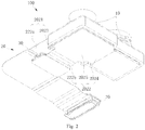
- Fig. 2 is a schematic isometric view of the imaging module of Fig. 1 from another viewing direction.
- Fig. 3 is an exploded isometric view of the imaging module of Fig. 1 .
- each of the two cameras 10 includes a printed circuit board 12, an image sensor (not shown), and a lens assembly 13.
- the image sensor is disposed on the printed circuit board 12.
- the lens assembly 13 is located above the image sensor.
- the two printed circuit boards 12 are spaced apart.
- the flexible printed circuit board 20 is coupled to the printed circuit boards 12.
- the two printed circuit boards 12 are spaced apart such that the two cameras 10 are spaced apart, which is beneficial for adjusting the optical axes of the two cameras 10 in parallel.
- one of the cameras 10 can be firstly held by a robot, then the position of the other camera 10 is adjusted by another robot until the optical axes of the two cameras 10 are parallel to each other and the two cameras 10 are identically oriented, and finally the two cameras 10 are secured by means of welding or dispensing.
- the image sensor is, for example, a complementary metal oxide semiconductor (CMOS) image sensor or a charge-coupled device (CCD) image sensor.
- CMOS complementary metal oxide semiconductor
- CCD charge-coupled device
- the image sensor can capture an image of the object, covert it into electrical signals, and transmit the signals to an external module via the printed circuit board 12 and the flexible printed circuit board 20. It should be noted that, the sensing surfaces of the two image sensors are identically oriented.
- Each of the lens assemblies 13 may include a voice coil motor and a lens disposed in the voice coil motor.
- the voice coil motor can drive the lens to move along the optical axis direction of the lens, so as to adjust a distance between the lens and the image sensor and in turn achieve auto-focus of the imaging module 100, thereby enabling the imaging module 100 to shoot images of fine quality.
- the lenses of the lens assemblies 13 of the two cameras 10 are a wide-angle lens and a telephoto lens, respectively. It will be appreciated that the wide-angle lens has a large shooting angle, while the telephoto lens has a small depth of field.
- the imaging module 100 can achieve optical zoom function by combining the wide-angle lens and the telephoto lens, thereby enabling the electronic device having the imaging module 100 to shoot images of high quality.
- the flexible printed circuit board 20 includes two flexible printed circuit sub-boards 202, and accordingly, the projection portion 22 includes two projection sub-portions 222 included by the two flexible printed circuit sub-boards 202, respectively.
- the two flexible printed circuit sub-boards 202 are coupled to the printed circuit boards 12, respectively, and the two projection sub-portions 222 are arranged to be stacked.
- the two flexible printed circuit sub-boards 202 are connected to the two cameras 10, respectively, thereby facilitating controlling the shooting by each camera 10 and in turn enabling the imaging module 100 to shoot images of fine quality.
- the two flexible printed circuit sub-boards 202 are a first flexible printed circuit sub-board 2021 and a second flexible printed circuit sub-board 2022.
- the first flexible printed circuit sub-board 2021 includes a first connection portion 2023 coupled to the printed circuit board 12 of the one camera 10 and a first projection sub-portion 222a projecting from the first connection portion 2023 and beyond the side edge of the imaging unit 11.
- the second flexible printed circuit sub-board 2022 includes a second connection portion 2024 coupled to the printed circuit board 12 of the other camera 10, an extension portion 2025, and a second projection sub-portion 222b.
- the extension portion 2025 extends from the second connection portion 2024 towards the first connection portion 2023, and in turn covers the first connection portion 2023.
- the second projection sub-portion 222b projects from the extension portion 2025 and beyond the side edge of the imaging unit 11.
- the first projection sub-portion 222a and the second projection sub-portion 222b are arranged to be stacked.
- the first flexible printed circuit sub-board 2021 is connected to the camera 10 on the left, while the second flexible printed circuit sub-board 2022 is connected to the camera 10 on the right.
- the first flexible printed circuit sub-board 2021 may be connected to the camera 10 on the right, while the second flexible printed circuit sub-board 2022 may be connected to the camera 10 on the left.
- the first projection sub-portion 222a includes a first projection section 2221 and a second projection section 2223.
- the first projection section 2221 projects to the one camera 10
- the second projection section 2223 is connected to one end of the first projection section 2221 away from the one camera 10 and projects along the arranging direction of the two cameras 10.
- the second projection sub-portion 222b has a length smaller than the first projection section 2221.
- the second projection section 2223 may be removed, and in this case, the first projection sub-portion 222a may has a length less than or equal to the second projection sub-portion 222b.
- the imaging module 100 further includes two connectors 30.
- One connector 30 is provided on a first surface of the first projection sub-portion 222a, while the other connector 30 is provided on a second surface of the second projection sub-portion 222b. The second surface is opposite the first surface.
- the connectors 30 are configured for being connected to external circuits.
- the imaging module 100 can be quickly mounted in the electronic device by means of the connectors 30 disposed on the two opposite surfaces of the first projection sub-portion 222a and the second projection sub-portion 222b, thereby facilitating mounting the imaging module 100 onto two opposite sides of a circuit board.
- the imaging module 100 further includes a cuboid housing 40.
- the two cameras 10 are disposed in the housing 40 and undetachably connected to the housing 40.
- the housing 40 can improve the stability of the two cameras 10 and prevent the optical axes of the two cameras 10 from being misaligned to affect imaging quality of the imaging module 100 when the imaging module 100 is impacted.
- the housing 40 includes a frame 42 and a cover plate 44. As illustrated in Fig. 3 , the frame 42 surrounds the two cameras 10, and the cover plate 44 is connected to the top of the frame 42. The cover plate 44 is provided with a through hole 46 through which the two cameras 10 are exposed so as to be capable of shooting. The two cameras 10 may be undetachably connected to the housing 40 by means of welding or dispensing.
- the housing 40 is formed by stamping a stainless steel plate having a thickness greater than or equal to 0.5 mm.
- the thickness of the housing 40 is 0.6mm, 0.8mm, or the like.
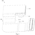
- FIG. 4 is a schematic isometric view of an imaging module according to another implementation of the present disclosure.
- an imaging module 200 is the same as the foregoing imaging module 100, except that two image sensors are disposed on a single continuous printed circuit board 212 and a single continuous flexible printed circuit board 220 is coupled to the printed circuit board 212.
- two cameras 210 share the printed circuit board 212, and the number of the flexible printed circuit board 220 is only one.
- the number of components of the imaging module 200 is reduced, thereby simplifying processes for manufacturing the imaging module 200 and improving efficiency of manufacturing the imaging module 200.
- the flexible printed circuit board 220 includes a projection portion 221 projecting from a side edge of the printed circuit board 212.
- the projection portion 221 includes a first elongation portion 2212 coupled to the printed circuit board 212 and a second elongation portion 2214. As illustrated in Fig. 4 , the second elongation 2214 elongates along the arranging direction of the two cameras 210 from one end of the first elongation portion 2212 away from the printed circuit board 212.
- the second elongation portion 2214 may be removed.
- the flexible printed circuit board 220 is a four-layered board. In other words, the flexible printed circuit board 220 has four layers, thereby meeting requirements of wires of the imaging assembly 200.
- the description of the imaging module 100 is also applicable to the imaging module 200. Aspects of the imaging module 200 not described may be identical or similar to those of the imaging module 100, and are not repeated herein.
- Fig. 5 is a schematic structural view of an electronic device according to an implementation of the present disclosure.
- Fig. 6 is a schematic plan view of the electronic device.
- an electronic device 1000 includes a main circuit board 310 and an imaging module 100(200) according to any one of the foregoing implementations.
- the electronic device 1000 is, for example, a mobile phone or a tablet computer.
- the main circuit board 310 is provided with an antenna area 314.
- the flexible printed circuit board 20(220) does not overlap the antenna area 314, and is coupled to the main circuit board 310. It will be appreciated that, an antenna 312 of the electronic device 1000 is located within the antenna area 314.
- the flexible printed circuit board 20(220) does not overlap the antenna area 314, i.e., the flexible printed circuit board 20(220) does not cover the antenna 312 in the antenna area 314, such that the antenna 312 can normally receive and transmit signals so as to enable the electronic device 1000 to normally communicate.
- the antenna 312 is interrupted at the position of the projection portion 22(221), such that the flexible printed circuit board 20(220) does not cover the antenna 312.
- the main circuit board 310 is located between the first projection sub-portion 222a and the second projection sub-portion 222b so as to render the structure of the electronic device 1000 more compact.
- the two cameras of the imaging module 100(200) are front cameras.
- the two cameras 10(210) have a shooting orientation identical to the displaying orientation of the display 1100 of the electronic device 1000, such that the two cameras 10(210) faces the user when the user uses the electronic device 1000 normally.
- the front two cameras 10(210) can improve the quality of the images when the user uses the electronic device 1000 to take a photograph of himself/herself, thereby improving user experience.
- the two cameras of the imaging module 100(200) may also be rear cameras.
- imaging module 200 may be identical or similar to those of the aforementioned imaging module 100 or 200, and are not repeated herein.
- the imaging module 100(200) and the electronic device 1000 of the present disclosure since the ratio of the width W of the projection portion 22 to the length L of the side edge ranges from 1/3 to 2/3, the area covered by the flexible printed circuit board 20 is small, thereby facilitating the arrangement of the electronic elements of the electronic device.
Landscapes
- Engineering & Computer Science (AREA)
- Signal Processing (AREA)
- Multimedia (AREA)
- Human Computer Interaction (AREA)
- Studio Devices (AREA)
- Camera Bodies And Camera Details Or Accessories (AREA)
- Telephone Set Structure (AREA)
- Cameras In General (AREA)
Abstract
Description
- The present application claims priority to Chinese Patent Application No.
201611121719.6 filed on December 8, 2016 - The present disclosure relates to electronic equipment, and more particularly, to an imaging module and an electronic device including the imaging module.
- A dual-camera module includes two cameras arranged side by side, and accordingly, two flexible printed circuit boards are also arranged side by side so as to transmit data, respectively. However, when the dual-camera module is arranged in an electronic device such as a mobile phone or a tablet computer, the two flexible printed circuit boards cover a large area and thus significantly affect electrical performance of electronic elements in the electronic device, which is not beneficial for arranging the electronic elements.
- The present disclosure is intended to provide an imaging module and an electronic device including the imaging module.
- In one aspect of the present disclosure, an imaging module is provided. The imaging module includes a flexible printed circuit board and an imaging unit including two cameras arranged side by side and connected to the flexible printed circuit board. The flexible printed circuit board includes a projection portion projecting to a side edge of the imaging unit. The side edge extends along an arranging direction of the two cameras, and a width of the projection portion in the arranging direction is less than a length of the side edge.
- According to the present disclosure, since the width of the projection portion in the arranging direction is less than the length of the side edge, the flexible printed circuit board covers a small area, which is beneficial for arranging electronic elements in the electronic device and ports configured for transmitting and receiving wireless signals can be exposed so as to enable transmission and reception of the wireless signals and ensure normal operation of the electronic device.
- In another aspect of the present disclosure, an electronic device is provided. The electronic device includes a main circuit board and an imaging module. The imaging module includes a flexible printed circuit board coupled to the main circuit board and an imaging unit including two cameras arranged side by side and connected to the flexible printed circuit board. The flexible printed circuit board includes a projection portion projecting to a side edge of the imaging unit. The side edge extends along an arranging direction of the two cameras, and a width of the projection portion in the arranging direction is less than a length of the side edge.
- According to the present disclosure, since the width of the projection portion in the arranging direction is less than the length of the side edge, the flexible printed circuit board covers a small area, which is beneficial for arranging electronic elements in the electronic device and ports configured for transmitting and receiving wireless signals can be exposed so as to enable transmission and reception of the wireless signals and ensure normal operation of the electronic device.
- The foregoing and/or additional aspects and advantages of the present disclosure will become apparent and better understood from the following description of the implementations taken in conjunction with the accompanying drawings.
-
Fig. 1 is a schematic isometric view of an imaging module according to an implementation of the present disclosure. -
Fig. 2 is a schematic isometric view of the imaging module ofFig. 1 from another viewing direction. -
Fig. 3 is an exploded isometric view of the imaging module ofFig. 1 . -
Fig. 4 is a schematic isometric view of an imaging module according to another implementation of the present disclosure. -
Fig. 5 is a schematic structural view of an electronic device according to an implementation of the present disclosure. -
Fig. 6 is a schematic plan view of an electronic device according to an implementation of the present disclosure. - Detailed implementations of the present disclosure are disclosed herein, and examples in the implementations are shown in the drawings in which identical or similar reference numbers and/or letters represent identical or similar parts or parts having identical or similar functions throughout. The implementations described with reference to the drawings below are merely exemplary for the purpose of explaining the present disclosure, and are not intended to limit the present disclosure.
- In the description of the present disclosure, it should be understood that orientational or positional relationships indicated by the terms "central", "longitudinal", "transverse", "length", "width", "thickness", "upper", "lower", "front", "back", "left", "right", "vertical", "horizontal", "top", "bottom", "inside", "outside", "clockwise", "counterclockwise", and the like are those as illustrated in the accompanying drawings, and are merely for facilitating and simplifying the description of the present disclosure, rather than indicating or implying that the mentioned devices or elements should have specific orientations and should be constructed and operated in specific orientations, and thus cannot be construed as a limit to the present disclosure.
- In addition, the terms "first", "second" are merely for illustrative purposes, and cannot be construed as indicating or implying relative importance or implicitly indicating the quantity of mentioned technical features. Therefore, explicitly or implicitly, features defined by "first", "second" may be one or more. In the description of the present disclosure, the term "plural" means two or more, unless specified otherwise.
- In the present disclosure, unless specified otherwise, the terms "mount", "connect", "couple", and the like should be broadly understood, and may include, for example, an undetachable connection, a detachable connection, an integral connection, a mechanical connection, an electrical connection, a direct connection, an indirect connection via an intermediate medium, a communication between two elements, and an interaction relationship between two elements. For persons skilled in the art, the specific meaning of the foregoing terms in the present disclosure should be understood in light of the specific circumstance.
- In the present disclosure, unless specified otherwise, the first feature being "on" or "beneath" the second feature may mean that the first feature may be in direct contact with the second feature, or the first feature may be in indirect contact with the second feature via an intermediate medium. Moreover, the first feature being "on", "over" or "above" the second feature may mean that the first feature is over or above the second feature, or merely mean that the first feature has a horizontal level higher than the second feature. The first feature being "beneath", "under" or "below" the second feature may mean that the first feature is under or below the second feature, or merely mean that the first feature has a horizontal level lower than the second feature.
- Many different implementations or examples for achieve different structures of the present disclosure are provided hereinafter. To simplify the present disclosure, the components and arrangements of specific examples are described below. These components and arrangements are merely exemplary, and are not to be construed as a limit to the present disclosure. In addition, the reference numbers and/or letters may be repeated in the different examples of the present disclosure. Such repetition is for the purpose of simplification and clarity, without indicating relationships between the discussed various implementations and/or arrangements. Moreover, the present disclosure provides examples of various specific processes and materials, but the application of other processes and/or other materials may also be appreciated by persons skilled in the art.
-
Fig. 1 is a schematic isometric view of an imaging module according to an implementation of the present disclosure. As illustrated inFig. 1 , animaging module 100 includes animaging unit 11 and a flexibleprinted circuit board 20. Theimaging unit 11 includes twocameras 10 which are arranged side by side and connected to the flexible printedcircuit board 20. The twocameras 10 can operate cooperatively or independently of each other. The flexible printedcircuit board 20 includes aprojection portion 22 projecting to a side edge of theimaging unit 11. The side edge extends along an arranging direction of the twocameras 10. In one implementation, as illustrated inFig. 1 , theprojection portion 22 projects along a direction perpendicular to the arranging direction. Theprojection portion 22 has a width W in the arranging direction which is less than a length L of the side edge in the arranging direction. The ratio of the width W of theprojection portion 22 to the length L of the side edge of theimaging unit 11 ranges from 1/3 to 2/3 (1/3<W/L<2/3). - In the
imaging module 100 according to the implementation of the present disclosure, since the ratio of the width W of theprojection portion 22 to the length L of the side edge ranges from 1/3 to 2/3, the flexible printedcircuit board 20 covers a small area, which is beneficial for arranging electronic elements in the electronic device. - The electronic elements may be, for example, ports which is located in the electronic device and configured for transmitting and receiving wireless signals. Since the width W of the
projection portion 22 of the flexible printedcircuit board 20 is small, the ports configured for transmitting and receiving wireless signals can be exposed so as to enable transmission and reception of the wireless signals and ensure normal operation of the electronic device. - In at least one implementation, the length of the side edge of the
imaging unit 11 is sufficiently large, and theprojection portion 22 projects to the side edge of theimaging unit 11 to be capable of ensuring that the flexible printedcircuit board 20 has a sufficient width, thereby meeting requirements of arranging wires on the flexible printedcircuit board 20 and in turn ensuring shooting function of theimaging module 100. - In one implementation, the ratio of the width W of the
projection portion 22 to the length L of the side edge of theimaging unit 11 ranges from 1/3 to 1/2. As a result, the area covered by theprojection portion 22 is smaller, and the electrical performance of the electronic elements near the flexible printedcircuit board 20 can be ensured. - In one implementation, the length L of the side edge of the
imaging unit 11 is 8 to 12 mm, and the width W of theprojection portion 22 is 4 to 6 mm. For example, the length L of the side edge of theimaging unit 11 is 10 mm, and the width W of theprojection portion 22 is 5 mm. In other words, the ratio of the width W of theprojection portion 22 to the length L of the side edge of theimaging unit 11 is 1/2 (W/L=1/2). - In one implementation, as illustrated in
Fig. 1 , theprojection portion 22 is merely located at one side of onecamera 10. In other words, the position of theprojection portion 22 corresponds to one of thecameras 10, and thus the flexible printedcircuit board 20 is not adjacent to theother camera 10, such that the electronic elements near theother camera 10 are not covered by the flexible printedcircuit board 20, thereby enabling the electronic elements functioning properly. In this case, the width of the projection portion may be no greater than a length of the onecamera 10 in the arranging direction of the twocameras 10. -
Fig. 2 is a schematic isometric view of the imaging module ofFig. 1 from another viewing direction.Fig. 3 is an exploded isometric view of the imaging module ofFig. 1 . As illustrated inFig. 2 andFig. 3 , in one implementation, each of the twocameras 10 includes a printedcircuit board 12, an image sensor (not shown), and alens assembly 13. The image sensor is disposed on the printedcircuit board 12. Thelens assembly 13 is located above the image sensor. The two printedcircuit boards 12 are spaced apart. The flexible printedcircuit board 20 is coupled to the printedcircuit boards 12. - The two printed
circuit boards 12 are spaced apart such that the twocameras 10 are spaced apart, which is beneficial for adjusting the optical axes of the twocameras 10 in parallel. In one implementation, when the twocameras 10 are assembled, one of thecameras 10 can be firstly held by a robot, then the position of theother camera 10 is adjusted by another robot until the optical axes of the twocameras 10 are parallel to each other and the twocameras 10 are identically oriented, and finally the twocameras 10 are secured by means of welding or dispensing. - The image sensor is, for example, a complementary metal oxide semiconductor (CMOS) image sensor or a charge-coupled device (CCD) image sensor. The image sensor can capture an image of the object, covert it into electrical signals, and transmit the signals to an external module via the printed
circuit board 12 and the flexible printedcircuit board 20. It should be noted that, the sensing surfaces of the two image sensors are identically oriented. - Each of the
lens assemblies 13 may include a voice coil motor and a lens disposed in the voice coil motor. The voice coil motor can drive the lens to move along the optical axis direction of the lens, so as to adjust a distance between the lens and the image sensor and in turn achieve auto-focus of theimaging module 100, thereby enabling theimaging module 100 to shoot images of fine quality. - In one implementation, the lenses of the
lens assemblies 13 of the twocameras 10 are a wide-angle lens and a telephoto lens, respectively. It will be appreciated that the wide-angle lens has a large shooting angle, while the telephoto lens has a small depth of field. Theimaging module 100 can achieve optical zoom function by combining the wide-angle lens and the telephoto lens, thereby enabling the electronic device having theimaging module 100 to shoot images of high quality. - As illustrated in
Fig. 2 andFig. 3 , in one implementation, the flexible printedcircuit board 20 includes two flexible printedcircuit sub-boards 202, and accordingly, theprojection portion 22 includes two projection sub-portions 222 included by the two flexible printedcircuit sub-boards 202, respectively. - The two flexible printed circuit sub-boards 202 are coupled to the printed
circuit boards 12, respectively, and the two projection sub-portions 222 are arranged to be stacked. - In this way, the two flexible printed circuit sub-boards 202 are connected to the two
cameras 10, respectively, thereby facilitating controlling the shooting by eachcamera 10 and in turn enabling theimaging module 100 to shoot images of fine quality. - In one implementation, the two flexible printed circuit sub-boards 202 are a first flexible printed
circuit sub-board 2021 and a second flexible printedcircuit sub-board 2022. As illustrated inFig. 2 , the first flexible printedcircuit sub-board 2021 includes afirst connection portion 2023 coupled to the printedcircuit board 12 of the onecamera 10 and afirst projection sub-portion 222a projecting from thefirst connection portion 2023 and beyond the side edge of theimaging unit 11. - The second flexible printed
circuit sub-board 2022 includes asecond connection portion 2024 coupled to the printedcircuit board 12 of theother camera 10, anextension portion 2025, and asecond projection sub-portion 222b. Theextension portion 2025 extends from thesecond connection portion 2024 towards thefirst connection portion 2023, and in turn covers thefirst connection portion 2023. Thesecond projection sub-portion 222b projects from theextension portion 2025 and beyond the side edge of theimaging unit 11. Thefirst projection sub-portion 222a and thesecond projection sub-portion 222b are arranged to be stacked. - As illustrated in
Fig. 2 , the first flexible printedcircuit sub-board 2021 is connected to thecamera 10 on the left, while the second flexible printedcircuit sub-board 2022 is connected to thecamera 10 on the right. Naturally, in other implementations, the first flexible printedcircuit sub-board 2021 may be connected to thecamera 10 on the right, while the second flexible printedcircuit sub-board 2022 may be connected to thecamera 10 on the left. - In one implementation, as illustrated in
Fig. 1 , thefirst projection sub-portion 222a includes afirst projection section 2221 and asecond projection section 2223. Thefirst projection section 2221 projects to the onecamera 10, and thesecond projection section 2223 is connected to one end of thefirst projection section 2221 away from the onecamera 10 and projects along the arranging direction of the twocameras 10. Thesecond projection sub-portion 222b has a length smaller than thefirst projection section 2221. - Naturally, in other implementations, the
second projection section 2223 may be removed, and in this case, thefirst projection sub-portion 222a may has a length less than or equal to thesecond projection sub-portion 222b. - In one implementation, as illustrated in
Fig. 2 , theimaging module 100 further includes twoconnectors 30. Oneconnector 30 is provided on a first surface of thefirst projection sub-portion 222a, while theother connector 30 is provided on a second surface of thesecond projection sub-portion 222b. The second surface is opposite the first surface. Theconnectors 30 are configured for being connected to external circuits. - As such, the
imaging module 100 can be quickly mounted in the electronic device by means of theconnectors 30 disposed on the two opposite surfaces of thefirst projection sub-portion 222a and thesecond projection sub-portion 222b, thereby facilitating mounting theimaging module 100 onto two opposite sides of a circuit board. - In one implementation, the
imaging module 100 further includes acuboid housing 40. The twocameras 10 are disposed in thehousing 40 and undetachably connected to thehousing 40. - The
housing 40 can improve the stability of the twocameras 10 and prevent the optical axes of the twocameras 10 from being misaligned to affect imaging quality of theimaging module 100 when theimaging module 100 is impacted. - In one implementation, the
housing 40 includes aframe 42 and acover plate 44. As illustrated inFig. 3 , theframe 42 surrounds the twocameras 10, and thecover plate 44 is connected to the top of theframe 42. Thecover plate 44 is provided with a throughhole 46 through which the twocameras 10 are exposed so as to be capable of shooting. The twocameras 10 may be undetachably connected to thehousing 40 by means of welding or dispensing. - In order to ensure the strength of the connection between the
housing 40 and the twocameras 10, thehousing 40 is formed by stamping a stainless steel plate having a thickness greater than or equal to 0.5 mm. For example, the thickness of thehousing 40 is 0.6mm, 0.8mm, or the like. -
Fig. 4 is a schematic isometric view of an imaging module according to another implementation of the present disclosure. As illustrated inFig. 4 , animaging module 200 is the same as the foregoingimaging module 100, except that two image sensors are disposed on a single continuous printedcircuit board 212 and a single continuous flexible printedcircuit board 220 is coupled to the printedcircuit board 212. In other words, twocameras 210 share the printedcircuit board 212, and the number of the flexible printedcircuit board 220 is only one. - In this way, the number of components of the
imaging module 200 is reduced, thereby simplifying processes for manufacturing theimaging module 200 and improving efficiency of manufacturing theimaging module 200. - In one implementation, the flexible printed
circuit board 220 includes aprojection portion 221 projecting from a side edge of the printedcircuit board 212. Theprojection portion 221 includes afirst elongation portion 2212 coupled to the printedcircuit board 212 and asecond elongation portion 2214. As illustrated inFig. 4 , thesecond elongation 2214 elongates along the arranging direction of the twocameras 210 from one end of thefirst elongation portion 2212 away from the printedcircuit board 212. - Naturally, in other implementations, the
second elongation portion 2214 may be removed. - In one implementation, the flexible printed
circuit board 220 is a four-layered board. In other words, the flexible printedcircuit board 220 has four layers, thereby meeting requirements of wires of theimaging assembly 200. - It is to be noted that, the description of the
imaging module 100 is also applicable to theimaging module 200. Aspects of theimaging module 200 not described may be identical or similar to those of theimaging module 100, and are not repeated herein. -
Fig. 5 is a schematic structural view of an electronic device according to an implementation of the present disclosure.Fig. 6 is a schematic plan view of the electronic device. As illustrated inFig. 5 , anelectronic device 1000 includes amain circuit board 310 and an imaging module 100(200) according to any one of the foregoing implementations. Theelectronic device 1000 is, for example, a mobile phone or a tablet computer. Themain circuit board 310 is provided with anantenna area 314. The flexible printed circuit board 20(220) does not overlap theantenna area 314, and is coupled to themain circuit board 310. It will be appreciated that, anantenna 312 of theelectronic device 1000 is located within theantenna area 314. - The flexible printed circuit board 20(220) does not overlap the
antenna area 314, i.e., the flexible printed circuit board 20(220) does not cover theantenna 312 in theantenna area 314, such that theantenna 312 can normally receive and transmit signals so as to enable theelectronic device 1000 to normally communicate. As illustrated inFig. 5 , theantenna 312 is interrupted at the position of the projection portion 22(221), such that the flexible printed circuit board 20(220) does not cover theantenna 312. - In one implementation, the
main circuit board 310 is located between thefirst projection sub-portion 222a and thesecond projection sub-portion 222b so as to render the structure of theelectronic device 1000 more compact. - In one implementation, the two cameras of the imaging module 100(200) are front cameras. In other words, the two cameras 10(210) have a shooting orientation identical to the displaying orientation of the
display 1100 of theelectronic device 1000, such that the two cameras 10(210) faces the user when the user uses theelectronic device 1000 normally. The front two cameras 10(210) can improve the quality of the images when the user uses theelectronic device 1000 to take a photograph of himself/herself, thereby improving user experience. - In other implementations, the two cameras of the imaging module 100(200) may also be rear cameras.
- It is to be noted that, aspects of the
imaging module 200 which are not described may be identical or similar to those of theaforementioned imaging module - As explained above, according to the imaging module 100(200) and the
electronic device 1000 of the present disclosure, since the ratio of the width W of theprojection portion 22 to the length L of the side edge ranges from 1/3 to 2/3, the area covered by the flexible printedcircuit board 20 is small, thereby facilitating the arrangement of the electronic elements of the electronic device. - In the present disclosure, the description of the terms "one implementation", "exemplary implementation", "example", "embodiment", "some examples", or the like are intended to mean that specific features, structures, materials, or characteristics described in conjunction with the implementations or examples are included in at least one implementation or example of the present disclosure. In the specification, the exemplary description of the foregoing terms does not necessarily refer to the same implementations or examples. Moreover, the described specific features, structures, materials, or characteristics may be combined in an appropriate way in any one or more implementations or examples.
- Although the implementations of the present disclosure have been illustrated and described, it should be understood by persons skilled in the art that various changes, modifications, substitutions, and variations could be made to these implementations without departing from the principles and spirits of the present disclosure. The scope of the present disclosure is defined by claims and equivalents thereof.
Claims (15)
- An imaging module, comprising:a flexible printed circuit board; andan imaging unit comprising two cameras arranged side by side and connected to the flexible printed circuit board;the flexible printed circuit board comprising a projection portion projecting to a side edge of the imaging unit, the side edge extending along an arranging direction of the two cameras, and a width of the projection portion in the arranging direction being less than a length of the side edge.
- The imaging module of claim 1, wherein a ratio of the width of the projection portion to the length of the side edge of the imaging unit ranges from 1/3 to 2/3.
- The imaging module of claim 1, wherein the projection portion is located at one side of one of the two cameras.
- The imaging module of claim 3, wherein the width of the projection portion is no greater than a length of the one of the two cameras in the arranging direction.
- The imaging module of any one of claims 1 to 4, wherein each of the two cameras comprises a printed circuit board, an image sensor disposed on the printed circuit board, and a lens assembly located above the image sensor, wherein the two printed circuit boards are spaced apart, and the flexible printed circuit board is coupled to the two printed circuit boards.
- The imaging module of claim 5, wherein the flexible printed circuit board further comprises:a first connection portion coupled to the printed circuit board of the one of the two cameras; anda second connection portion coupled to the printed circuit board of the other of the two cameras.
- The imaging module of claim 6, wherein the flexible printed circuit board further comprises an extension portion extending from the second connection portion towards the first connection portion and covering the first connection portion; and
the projection portion comprises a first projection sub-portion projecting from the first connection portion and beyond the side edge and a second projection sub-portion projecting from the extension portion and beyond the side edge, wherein the first projection sub-portion and the second projection sub-portion are arranged to be stacked. - The imaging module of any one of claims 1 to 4, wherein each of the two cameras comprises an image sensor and a lens assembly located above the image sensor, wherein the two image sensors are disposed on one printed circuit board, and the flexible printed circuit board is a single continuous flexible printed circuit board coupled to the printed circuit board.
- An electronic device, comprising:a main circuit board; andan imaging module comprising:a flexible printed circuit board coupled to the main circuit board; andan imaging unit comprising two cameras arranged side by side and connected to the flexible printed circuit board;the flexible printed circuit board comprising a projection portion projecting to a side edge of the imaging unit, the side edge extending along an arranging direction of the two cameras, and a width of the projection portion in the arranging direction being less than a length of the side edge.
- The electronic device of claim 9, wherein a ratio of the width of the projection portion to the length of the side edge of the imaging unit ranges from 1/3 to 2/3.
- The electronic device of claim 9, wherein the projection portion is located at one side of one of the two cameras.
- The electronic device of any one of claims 9 to 11, wherein each of the two cameras comprises a printed circuit board, an image sensor disposed on the printed circuit board, and a lens assembly located above the image sensor, wherein the two printed circuit boards are spaced apart, and the flexible printed circuit board is coupled to the two printed circuit boards.
- The electronic device of claim 12, wherein the flexible printed circuit board further comprises:a first connection portion coupled to the printed circuit board of the one of the two cameras; anda second connection portion coupled to the printed circuit board of the other of the two cameras.
- The electronic device of claim 13, wherein the flexible printed circuit board further comprises an extension portion extending from the second connection portion towards the first connection portion and covering the first connection portion; and
the projection portion comprises a first projection sub-portion projecting from the first connection portion and beyond the side edge and a second projection sub-portion projecting from the extension portion and beyond the side edge, wherein the first projection sub-portion and the second projection sub-portion are arranged to be stacked, and the main circuit board is located between the first projection sub-portion and the second projection sub-portion. - The electronic device of any one of claims 9 to 11, wherein each of the two cameras comprises an image sensor and a lens assembly located above the image sensor, wherein the two image sensors are disposed on one printed circuit board, and the flexible printed circuit board is a single continuous flexible printed circuit board coupled to the printed circuit board.
Applications Claiming Priority (1)
| Application Number | Priority Date | Filing Date | Title |
|---|---|---|---|
| CN201611121719.6A CN106790792B (en) | 2016-12-08 | 2016-12-08 | Imaging modules and mobile terminals |
Publications (2)
| Publication Number | Publication Date |
|---|---|
| EP3334146A1 true EP3334146A1 (en) | 2018-06-13 |
| EP3334146B1 EP3334146B1 (en) | 2019-06-19 |
Family
ID=58877278
Family Applications (1)
| Application Number | Title | Priority Date | Filing Date |
|---|---|---|---|
| EP17201256.9A Active EP3334146B1 (en) | 2016-12-08 | 2017-11-13 | Imaging module and electronic device |
Country Status (5)
| Country | Link |
|---|---|
| US (1) | US10270952B2 (en) |
| EP (1) | EP3334146B1 (en) |
| CN (1) | CN106790792B (en) |
| ES (1) | ES2740873T3 (en) |
| WO (1) | WO2018103523A1 (en) |
Cited By (1)
| Publication number | Priority date | Publication date | Assignee | Title |
|---|---|---|---|---|
| CN110706584A (en) * | 2019-09-09 | 2020-01-17 | 武汉华星光电技术有限公司 | Backlight module and display device |
Families Citing this family (27)
| Publication number | Priority date | Publication date | Assignee | Title |
|---|---|---|---|---|
| US20170244265A1 (en) * | 2014-11-11 | 2017-08-24 | Guangdong Oppo Mobile Telecommunications Corp., Ltd. | Communication method, power adaptor and terminal |
| CN106790792B (en) * | 2016-12-08 | 2019-02-05 | Oppo广东移动通信有限公司 | Imaging modules and mobile terminals |
| CN106713540B (en) * | 2016-12-20 | 2019-12-06 | Oppo广东移动通信有限公司 | Double-camera module and mobile terminal |
| CN106791330B (en) * | 2017-01-11 | 2019-08-13 | Oppo广东移动通信有限公司 | Camera module and terminal |
| CN107343122A (en) * | 2017-08-02 | 2017-11-10 | 深圳奥比中光科技有限公司 | 3D imaging devices |
| US10268234B2 (en) * | 2017-08-07 | 2019-04-23 | Apple Inc. | Bracket assembly for a multi-component vision system in an electronic device |
| CN107592381A (en) * | 2017-08-22 | 2018-01-16 | 广东欧珀移动通信有限公司 | Cover assembly, casing assembly, processing method of casing assembly, and mobile terminal |
| CN110233911B (en) * | 2018-03-06 | 2021-07-30 | Oppo广东移动通信有限公司 | Imaging modules, camera components and electronic devices |
| CN110233913B (en) * | 2018-03-06 | 2021-07-20 | Oppo广东移动通信有限公司 | Housing, camera assembly and electronic device |
| CN110233912B (en) * | 2018-03-06 | 2021-04-13 | Oppo广东移动通信有限公司 | Camera components and electronic devices |
| CN110233951B (en) * | 2018-03-06 | 2021-02-19 | Oppo广东移动通信有限公司 | Camera module, camera assembly and electronic device |
| CN110248054B (en) * | 2018-03-09 | 2021-05-04 | Oppo广东移动通信有限公司 | Shell, camera module, camera assembly and electronic device |
| CN108174080B (en) * | 2018-03-20 | 2020-01-31 | 维沃移动通信有限公司 | camera module and mobile terminal |
| US11350020B2 (en) | 2018-05-30 | 2022-05-31 | Ningbo Sunny Opotech Co., Ltd. | Camera module array and assembly method therefor |
| CN110557523B (en) * | 2018-05-30 | 2024-03-05 | 宁波舜宇光电信息有限公司 | Camera module array and assembling method thereof |
| CN108900660B (en) * | 2018-06-02 | 2021-03-12 | Oppo广东移动通信有限公司 | Electronic component and electronic equipment |
| CN111327731A (en) * | 2018-12-14 | 2020-06-23 | 北京小米移动软件有限公司 | foldable terminal |
| US20200236254A1 (en) * | 2019-01-23 | 2020-07-23 | Black Seasme International Holding Limited | Camera system with reduced alignment shift |
| KR102805299B1 (en) * | 2019-07-26 | 2025-05-12 | 삼성전자주식회사 | Electronic device including electronic component assembly |
| CN113726988A (en) * | 2020-05-26 | 2021-11-30 | 黑芝麻智能科技(重庆)有限公司 | Alignment offset reduction system |
| EP4163760B1 (en) | 2020-07-14 | 2025-03-26 | Samsung Electronics Co., Ltd. | Electronic device comprising flexible display |
| EP4167050B1 (en) | 2020-07-14 | 2025-04-16 | Samsung Electronics Co., Ltd. | Electronic apparatus comprising flexible display |
| WO2022015012A1 (en) * | 2020-07-14 | 2022-01-20 | 삼성전자 주식회사 | Electronic device comprising flexible display |
| CN111917956B (en) * | 2020-08-05 | 2025-05-06 | 河南皓泽电子股份有限公司昆山分公司 | Camera module and camera device having the same |
| US12581206B1 (en) * | 2021-09-23 | 2026-03-17 | Apple Inc. | Single flex circuit shared by multiple cameras of a multi-camera system |
| EP4637123A4 (en) * | 2023-01-26 | 2026-03-25 | Samsung Electronics Co Ltd | ELECTRONIC DEVICE WITH FLEXIBLE CIRCUIT BOARD |
| US12568293B1 (en) * | 2024-08-28 | 2026-03-03 | Inuitive Ltd. | Stable 3D optical sensing device |
Citations (3)
| Publication number | Priority date | Publication date | Assignee | Title |
|---|---|---|---|---|
| CN105187697A (en) * | 2015-08-04 | 2015-12-23 | 宁波舜宇光电信息有限公司 | Multi-lens camera module one-piece bracket, multi-lens camera module and application of multi-lens camera module |
| CN105681637A (en) * | 2016-03-15 | 2016-06-15 | 宁波舜宇光电信息有限公司 | Array camera module and photosensitive assembly thereof and manufacturing method |
| CN205545547U (en) * | 2016-03-03 | 2016-08-31 | 南昌欧菲光电技术有限公司 | Imaging module and electronic device |
Family Cites Families (17)
| Publication number | Priority date | Publication date | Assignee | Title |
|---|---|---|---|---|
| JP4252910B2 (en) | 2004-02-13 | 2009-04-08 | セイコーインスツル株式会社 | Charge / discharge control circuit and rechargeable power supply |
| KR100649770B1 (en) * | 2005-12-29 | 2006-11-27 | 삼성전기주식회사 | Dual camera module of wireless communication terminal |
| KR101378880B1 (en) * | 2007-07-13 | 2014-03-28 | 엘지전자 주식회사 | Portable terminal having camera |
| JP4766095B2 (en) | 2008-10-09 | 2011-09-07 | ソニー株式会社 | Charger |
| TWI537670B (en) * | 2011-12-13 | 2016-06-11 | 鴻海精密工業股份有限公司 | Dual lens camera |
| CN103973943A (en) * | 2013-01-31 | 2014-08-06 | 鸿富锦精密工业(深圳)有限公司 | Double-camera module |
| CN103762702B (en) | 2014-01-28 | 2015-12-16 | 广东欧珀移动通信有限公司 | Charging device of electronic appliances and power supply adaptor thereof |
| US9474154B2 (en) * | 2014-07-18 | 2016-10-18 | Starkey Laboratories, Inc. | Reflow solderable flexible circuit board — to — flexible circuit board connector reinforcement |
| KR102257809B1 (en) * | 2014-08-29 | 2021-05-28 | 삼성전자 주식회사 | Electronic device having a camera module protection structure |
| CN104993562B (en) | 2015-08-05 | 2017-12-05 | 青岛海信移动通信技术股份有限公司 | Can directly be charged source adapter |
| CN107040699B (en) * | 2016-02-03 | 2019-11-26 | 台湾东电化股份有限公司 | photography device |
| CN205545553U (en) * | 2016-03-03 | 2016-08-31 | 南昌欧菲光电技术有限公司 | Imaging module and electronic device |
| EP3429181B1 (en) * | 2016-03-12 | 2024-10-16 | Ningbo Sunny Opotech Co., Ltd. | Array camera module, moulded photosensitive assembly and manufacturing method therefor, and electronic device |
| CN105827915B (en) * | 2016-04-22 | 2019-09-03 | 上海青橙实业有限公司 | Cam device and mobile terminal |
| KR101785458B1 (en) * | 2016-06-07 | 2017-10-16 | 엘지전자 주식회사 | Camera module and mobile terminal having the same |
| CN106790792B (en) * | 2016-12-08 | 2019-02-05 | Oppo广东移动通信有限公司 | Imaging modules and mobile terminals |
| CN207010790U (en) * | 2017-04-17 | 2018-02-13 | 三赢科技(深圳)有限公司 | Imaging module |
-
2016
- 2016-12-08 CN CN201611121719.6A patent/CN106790792B/en not_active Expired - Fee Related
-
2017
- 2017-11-13 EP EP17201256.9A patent/EP3334146B1/en active Active
- 2017-11-13 ES ES17201256T patent/ES2740873T3/en active Active
- 2017-11-20 WO PCT/CN2017/111804 patent/WO2018103523A1/en not_active Ceased
- 2017-11-30 US US15/826,937 patent/US10270952B2/en active Active
Patent Citations (3)
| Publication number | Priority date | Publication date | Assignee | Title |
|---|---|---|---|---|
| CN105187697A (en) * | 2015-08-04 | 2015-12-23 | 宁波舜宇光电信息有限公司 | Multi-lens camera module one-piece bracket, multi-lens camera module and application of multi-lens camera module |
| CN205545547U (en) * | 2016-03-03 | 2016-08-31 | 南昌欧菲光电技术有限公司 | Imaging module and electronic device |
| CN105681637A (en) * | 2016-03-15 | 2016-06-15 | 宁波舜宇光电信息有限公司 | Array camera module and photosensitive assembly thereof and manufacturing method |
Cited By (1)
| Publication number | Priority date | Publication date | Assignee | Title |
|---|---|---|---|---|
| CN110706584A (en) * | 2019-09-09 | 2020-01-17 | 武汉华星光电技术有限公司 | Backlight module and display device |
Also Published As
| Publication number | Publication date |
|---|---|
| US20180167540A1 (en) | 2018-06-14 |
| EP3334146B1 (en) | 2019-06-19 |
| CN106790792B (en) | 2019-02-05 |
| ES2740873T3 (en) | 2020-02-06 |
| CN106790792A (en) | 2017-05-31 |
| US10270952B2 (en) | 2019-04-23 |
| WO2018103523A1 (en) | 2018-06-14 |
Similar Documents
| Publication | Publication Date | Title |
|---|---|---|
| US10270952B2 (en) | Imaging module with two cameras and electronic device | |
| JP4084367B2 (en) | Camera module shake correction device | |
| US8861946B2 (en) | Device for driving camera lens module in portable terminal | |
| EP3349064B1 (en) | Camera module applied to terminal and terminal including same | |
| US7295390B2 (en) | Lens actuating device, camera module and portable electronic equipment | |
| EP3573324B1 (en) | Camera assembly and electronic apparatus | |
| US20150256730A1 (en) | Image-capturing device configured for a handheld electronic device | |
| TWI611248B (en) | 360 degree panoramic camera module and apparatus | |
| US20180367720A1 (en) | Dual camera module and electronic apparatus using same | |
| CN108632412A (en) | A kind of photographic device and mobile terminal | |
| US8520136B2 (en) | Small industrial electronic imaging camera | |
| KR100645653B1 (en) | Mobile phone camera module and its control device | |
| CN221572982U (en) | Imaging lens module with changeable light hole module, camera module and electronic device | |
| KR101859380B1 (en) | Multi-camera device | |
| CN107241538B (en) | Imaging device, imaging device assembly, and electronic device | |
| CN107147835B (en) | electronic device | |
| CN105556388B (en) | Camera module | |
| CN108418919A (en) | Electronic device and control method thereof | |
| CN116261036A (en) | Periscope camera module and electronic device | |
| CN220307288U (en) | Movable circuit element, movable electronic photosensitive module, camera module and electronic device | |
| CN107155046A (en) | Imaging Modules and Electronic Devices | |
| TW201508699A (en) | Recorder for vehicle | |
| CN107155024A (en) | Imaging module and electronic device | |
| KR20090004349U (en) | Camera module | |
| JP2016015661A (en) | Imaging device with wireless communication function |
Legal Events
| Date | Code | Title | Description |
|---|---|---|---|
| PUAI | Public reference made under article 153(3) epc to a published international application that has entered the european phase |
Free format text: ORIGINAL CODE: 0009012 |
|
| STAA | Information on the status of an ep patent application or granted ep patent |
Free format text: STATUS: REQUEST FOR EXAMINATION WAS MADE |
|
| 17P | Request for examination filed |
Effective date: 20171113 |
|
| AK | Designated contracting states |
Kind code of ref document: A1 Designated state(s): AL AT BE BG CH CY CZ DE DK EE ES FI FR GB GR HR HU IE IS IT LI LT LU LV MC MK MT NL NO PL PT RO RS SE SI SK SM TR |
|
| AX | Request for extension of the european patent |
Extension state: BA ME |
|
| STAA | Information on the status of an ep patent application or granted ep patent |
Free format text: STATUS: EXAMINATION IS IN PROGRESS |
|
| 17Q | First examination report despatched |
Effective date: 20181123 |
|
| REG | Reference to a national code |
Ref country code: DE Ref legal event code: R079 Ref document number: 602017004663 Country of ref document: DE Free format text: PREVIOUS MAIN CLASS: H04N0005225000 Ipc: H04M0001020000 |
|
| GRAP | Despatch of communication of intention to grant a patent |
Free format text: ORIGINAL CODE: EPIDOSNIGR1 |
|
| STAA | Information on the status of an ep patent application or granted ep patent |
Free format text: STATUS: GRANT OF PATENT IS INTENDED |
|
| RIC1 | Information provided on ipc code assigned before grant |
Ipc: H04N 5/225 20060101ALI20190205BHEP Ipc: H04M 1/02 20060101AFI20190205BHEP |
|
| INTG | Intention to grant announced |
Effective date: 20190304 |
|
| RAP1 | Party data changed (applicant data changed or rights of an application transferred) |
Owner name: GUANGDONG OPPO MOBILE TELECOMMUNICATIONS CORP., LT |
|
| GRAS | Grant fee paid |
Free format text: ORIGINAL CODE: EPIDOSNIGR3 |
|
| GRAA | (expected) grant |
Free format text: ORIGINAL CODE: 0009210 |
|
| STAA | Information on the status of an ep patent application or granted ep patent |
Free format text: STATUS: THE PATENT HAS BEEN GRANTED |
|
| AK | Designated contracting states |
Kind code of ref document: B1 Designated state(s): AL AT BE BG CH CY CZ DE DK EE ES FI FR GB GR HR HU IE IS IT LI LT LU LV MC MK MT NL NO PL PT RO RS SE SI SK SM TR |
|
| REG | Reference to a national code |
Ref country code: GB Ref legal event code: FG4D |
|
| REG | Reference to a national code |
Ref country code: CH Ref legal event code: EP |
|
| REG | Reference to a national code |
Ref country code: IE Ref legal event code: FG4D |
|
| REG | Reference to a national code |
Ref country code: DE Ref legal event code: R096 Ref document number: 602017004663 Country of ref document: DE |
|
| REG | Reference to a national code |
Ref country code: AT Ref legal event code: REF Ref document number: 1146967 Country of ref document: AT Kind code of ref document: T Effective date: 20190715 |
|
| REG | Reference to a national code |
Ref country code: NL Ref legal event code: FP |
|
| PG25 | Lapsed in a contracting state [announced via postgrant information from national office to epo] |
Ref country code: LT Free format text: LAPSE BECAUSE OF FAILURE TO SUBMIT A TRANSLATION OF THE DESCRIPTION OR TO PAY THE FEE WITHIN THE PRESCRIBED TIME-LIMIT Effective date: 20190619 Ref country code: HR Free format text: LAPSE BECAUSE OF FAILURE TO SUBMIT A TRANSLATION OF THE DESCRIPTION OR TO PAY THE FEE WITHIN THE PRESCRIBED TIME-LIMIT Effective date: 20190619 Ref country code: SE Free format text: LAPSE BECAUSE OF FAILURE TO SUBMIT A TRANSLATION OF THE DESCRIPTION OR TO PAY THE FEE WITHIN THE PRESCRIBED TIME-LIMIT Effective date: 20190619 Ref country code: NO Free format text: LAPSE BECAUSE OF FAILURE TO SUBMIT A TRANSLATION OF THE DESCRIPTION OR TO PAY THE FEE WITHIN THE PRESCRIBED TIME-LIMIT Effective date: 20190919 Ref country code: AL Free format text: LAPSE BECAUSE OF FAILURE TO SUBMIT A TRANSLATION OF THE DESCRIPTION OR TO PAY THE FEE WITHIN THE PRESCRIBED TIME-LIMIT Effective date: 20190619 Ref country code: FI Free format text: LAPSE BECAUSE OF FAILURE TO SUBMIT A TRANSLATION OF THE DESCRIPTION OR TO PAY THE FEE WITHIN THE PRESCRIBED TIME-LIMIT Effective date: 20190619 |
|
| REG | Reference to a national code |
Ref country code: LT Ref legal event code: MG4D |
|
| PG25 | Lapsed in a contracting state [announced via postgrant information from national office to epo] |
Ref country code: BG Free format text: LAPSE BECAUSE OF FAILURE TO SUBMIT A TRANSLATION OF THE DESCRIPTION OR TO PAY THE FEE WITHIN THE PRESCRIBED TIME-LIMIT Effective date: 20190919 Ref country code: LV Free format text: LAPSE BECAUSE OF FAILURE TO SUBMIT A TRANSLATION OF THE DESCRIPTION OR TO PAY THE FEE WITHIN THE PRESCRIBED TIME-LIMIT Effective date: 20190619 Ref country code: RS Free format text: LAPSE BECAUSE OF FAILURE TO SUBMIT A TRANSLATION OF THE DESCRIPTION OR TO PAY THE FEE WITHIN THE PRESCRIBED TIME-LIMIT Effective date: 20190619 Ref country code: GR Free format text: LAPSE BECAUSE OF FAILURE TO SUBMIT A TRANSLATION OF THE DESCRIPTION OR TO PAY THE FEE WITHIN THE PRESCRIBED TIME-LIMIT Effective date: 20190920 |
|
| RAP2 | Party data changed (patent owner data changed or rights of a patent transferred) |
Owner name: GUANGDONG OPPO MOBILE TELECOMMUNICATIONS CORP., LT |
|
| REG | Reference to a national code |
Ref country code: AT Ref legal event code: MK05 Ref document number: 1146967 Country of ref document: AT Kind code of ref document: T Effective date: 20190619 |
|
| PG25 | Lapsed in a contracting state [announced via postgrant information from national office to epo] |
Ref country code: PT Free format text: LAPSE BECAUSE OF FAILURE TO SUBMIT A TRANSLATION OF THE DESCRIPTION OR TO PAY THE FEE WITHIN THE PRESCRIBED TIME-LIMIT Effective date: 20191021 Ref country code: SK Free format text: LAPSE BECAUSE OF FAILURE TO SUBMIT A TRANSLATION OF THE DESCRIPTION OR TO PAY THE FEE WITHIN THE PRESCRIBED TIME-LIMIT Effective date: 20190619 Ref country code: CZ Free format text: LAPSE BECAUSE OF FAILURE TO SUBMIT A TRANSLATION OF THE DESCRIPTION OR TO PAY THE FEE WITHIN THE PRESCRIBED TIME-LIMIT Effective date: 20190619 Ref country code: RO Free format text: LAPSE BECAUSE OF FAILURE TO SUBMIT A TRANSLATION OF THE DESCRIPTION OR TO PAY THE FEE WITHIN THE PRESCRIBED TIME-LIMIT Effective date: 20190619 Ref country code: EE Free format text: LAPSE BECAUSE OF FAILURE TO SUBMIT A TRANSLATION OF THE DESCRIPTION OR TO PAY THE FEE WITHIN THE PRESCRIBED TIME-LIMIT Effective date: 20190619 Ref country code: AT Free format text: LAPSE BECAUSE OF FAILURE TO SUBMIT A TRANSLATION OF THE DESCRIPTION OR TO PAY THE FEE WITHIN THE PRESCRIBED TIME-LIMIT Effective date: 20190619 |
|
| REG | Reference to a national code |
Ref country code: ES Ref legal event code: FG2A Ref document number: 2740873 Country of ref document: ES Kind code of ref document: T3 Effective date: 20200206 |
|
| PG25 | Lapsed in a contracting state [announced via postgrant information from national office to epo] |
Ref country code: SM Free format text: LAPSE BECAUSE OF FAILURE TO SUBMIT A TRANSLATION OF THE DESCRIPTION OR TO PAY THE FEE WITHIN THE PRESCRIBED TIME-LIMIT Effective date: 20190619 Ref country code: IS Free format text: LAPSE BECAUSE OF FAILURE TO SUBMIT A TRANSLATION OF THE DESCRIPTION OR TO PAY THE FEE WITHIN THE PRESCRIBED TIME-LIMIT Effective date: 20191019 |
|
| PG25 | Lapsed in a contracting state [announced via postgrant information from national office to epo] |
Ref country code: TR Free format text: LAPSE BECAUSE OF FAILURE TO SUBMIT A TRANSLATION OF THE DESCRIPTION OR TO PAY THE FEE WITHIN THE PRESCRIBED TIME-LIMIT Effective date: 20190619 |
|
| PG25 | Lapsed in a contracting state [announced via postgrant information from national office to epo] |
Ref country code: DK Free format text: LAPSE BECAUSE OF FAILURE TO SUBMIT A TRANSLATION OF THE DESCRIPTION OR TO PAY THE FEE WITHIN THE PRESCRIBED TIME-LIMIT Effective date: 20190619 Ref country code: PL Free format text: LAPSE BECAUSE OF FAILURE TO SUBMIT A TRANSLATION OF THE DESCRIPTION OR TO PAY THE FEE WITHIN THE PRESCRIBED TIME-LIMIT Effective date: 20190619 |
|
| PG25 | Lapsed in a contracting state [announced via postgrant information from national office to epo] |
Ref country code: IS Free format text: LAPSE BECAUSE OF FAILURE TO SUBMIT A TRANSLATION OF THE DESCRIPTION OR TO PAY THE FEE WITHIN THE PRESCRIBED TIME-LIMIT Effective date: 20200224 |
|
| REG | Reference to a national code |
Ref country code: DE Ref legal event code: R097 Ref document number: 602017004663 Country of ref document: DE |
|
| PLBE | No opposition filed within time limit |
Free format text: ORIGINAL CODE: 0009261 |
|
| STAA | Information on the status of an ep patent application or granted ep patent |
Free format text: STATUS: NO OPPOSITION FILED WITHIN TIME LIMIT |
|
| PG2D | Information on lapse in contracting state deleted |
Ref country code: IS |
|
| PG25 | Lapsed in a contracting state [announced via postgrant information from national office to epo] |
Ref country code: MC Free format text: LAPSE BECAUSE OF FAILURE TO SUBMIT A TRANSLATION OF THE DESCRIPTION OR TO PAY THE FEE WITHIN THE PRESCRIBED TIME-LIMIT Effective date: 20190619 Ref country code: LU Free format text: LAPSE BECAUSE OF NON-PAYMENT OF DUE FEES Effective date: 20191113 |
|
| 26N | No opposition filed |
Effective date: 20200603 |
|
| REG | Reference to a national code |
Ref country code: BE Ref legal event code: MM Effective date: 20191130 |
|
| PG25 | Lapsed in a contracting state [announced via postgrant information from national office to epo] |
Ref country code: SI Free format text: LAPSE BECAUSE OF FAILURE TO SUBMIT A TRANSLATION OF THE DESCRIPTION OR TO PAY THE FEE WITHIN THE PRESCRIBED TIME-LIMIT Effective date: 20190619 |
|
| PG25 | Lapsed in a contracting state [announced via postgrant information from national office to epo] |
Ref country code: IE Free format text: LAPSE BECAUSE OF NON-PAYMENT OF DUE FEES Effective date: 20191113 |
|
| PG25 | Lapsed in a contracting state [announced via postgrant information from national office to epo] |
Ref country code: BE Free format text: LAPSE BECAUSE OF NON-PAYMENT OF DUE FEES Effective date: 20191130 |
|
| PG25 | Lapsed in a contracting state [announced via postgrant information from national office to epo] |
Ref country code: CY Free format text: LAPSE BECAUSE OF FAILURE TO SUBMIT A TRANSLATION OF THE DESCRIPTION OR TO PAY THE FEE WITHIN THE PRESCRIBED TIME-LIMIT Effective date: 20190619 |
|
| REG | Reference to a national code |
Ref country code: CH Ref legal event code: PL |
|
| PG25 | Lapsed in a contracting state [announced via postgrant information from national office to epo] |
Ref country code: HU Free format text: LAPSE BECAUSE OF FAILURE TO SUBMIT A TRANSLATION OF THE DESCRIPTION OR TO PAY THE FEE WITHIN THE PRESCRIBED TIME-LIMIT; INVALID AB INITIO Effective date: 20171113 Ref country code: MT Free format text: LAPSE BECAUSE OF FAILURE TO SUBMIT A TRANSLATION OF THE DESCRIPTION OR TO PAY THE FEE WITHIN THE PRESCRIBED TIME-LIMIT Effective date: 20190619 |
|
| PG25 | Lapsed in a contracting state [announced via postgrant information from national office to epo] |
Ref country code: CH Free format text: LAPSE BECAUSE OF NON-PAYMENT OF DUE FEES Effective date: 20201130 Ref country code: LI Free format text: LAPSE BECAUSE OF NON-PAYMENT OF DUE FEES Effective date: 20201130 |
|
| PG25 | Lapsed in a contracting state [announced via postgrant information from national office to epo] |
Ref country code: MK Free format text: LAPSE BECAUSE OF FAILURE TO SUBMIT A TRANSLATION OF THE DESCRIPTION OR TO PAY THE FEE WITHIN THE PRESCRIBED TIME-LIMIT Effective date: 20190619 |
|
| P01 | Opt-out of the competence of the unified patent court (upc) registered |
Effective date: 20230412 |
|
| PGFP | Annual fee paid to national office [announced via postgrant information from national office to epo] |
Ref country code: ES Payment date: 20231218 Year of fee payment: 7 |
|
| PGFP | Annual fee paid to national office [announced via postgrant information from national office to epo] |
Ref country code: IT Payment date: 20231110 Year of fee payment: 7 Ref country code: FR Payment date: 20231124 Year of fee payment: 7 |
|
| PG25 | Lapsed in a contracting state [announced via postgrant information from national office to epo] |
Ref country code: IT Free format text: LAPSE BECAUSE OF NON-PAYMENT OF DUE FEES Effective date: 20241113 |
|
| PG25 | Lapsed in a contracting state [announced via postgrant information from national office to epo] |
Ref country code: FR Free format text: LAPSE BECAUSE OF NON-PAYMENT OF DUE FEES Effective date: 20241130 |
|
| PGFP | Annual fee paid to national office [announced via postgrant information from national office to epo] |
Ref country code: NL Payment date: 20251127 Year of fee payment: 9 |
|
| REG | Reference to a national code |
Ref country code: ES Ref legal event code: FD2A Effective date: 20260105 |
|
| PGFP | Annual fee paid to national office [announced via postgrant information from national office to epo] |
Ref country code: DE Payment date: 20251124 Year of fee payment: 9 |
|
| PGFP | Annual fee paid to national office [announced via postgrant information from national office to epo] |
Ref country code: GB Payment date: 20251126 Year of fee payment: 9 |
|
| PG25 | Lapsed in a contracting state [announced via postgrant information from national office to epo] |
Ref country code: ES Free format text: LAPSE BECAUSE OF NON-PAYMENT OF DUE FEES Effective date: 20241114 |