EP3333861A1 - Power reception device and power transmission device - Google Patents
Power reception device and power transmission device Download PDFInfo
- Publication number
- EP3333861A1 EP3333861A1 EP17205559.2A EP17205559A EP3333861A1 EP 3333861 A1 EP3333861 A1 EP 3333861A1 EP 17205559 A EP17205559 A EP 17205559A EP 3333861 A1 EP3333861 A1 EP 3333861A1
- Authority
- EP
- European Patent Office
- Prior art keywords
- coil
- side wall
- power
- disposed
- power reception
- Prior art date
- Legal status (The legal status is an assumption and is not a legal conclusion. Google has not performed a legal analysis and makes no representation as to the accuracy of the status listed.)
- Granted
Links
Images





Classifications
-
- H—ELECTRICITY
- H02—GENERATION; CONVERSION OR DISTRIBUTION OF ELECTRIC POWER
- H02J—ELECTRIC POWER NETWORKS; CIRCUIT ARRANGEMENTS OR SYSTEMS FOR SUPPLYING OR DISTRIBUTING ELECTRIC POWER; SYSTEMS FOR STORING ELECTRIC ENERGY
- H02J50/00—Circuit arrangements or systems for wireless supply or distribution of electric power
- H02J50/005—Mechanical details of housing or structure aiming to accommodate the power transfer means, e.g. mechanical integration of coils, antennas or transducers into emitting or receiving devices
-
- B—PERFORMING OPERATIONS; TRANSPORTING
- B60—VEHICLES IN GENERAL
- B60L—PROPULSION OF ELECTRICALLY-PROPELLED VEHICLES; SUPPLYING ELECTRIC POWER FOR AUXILIARY EQUIPMENT OF ELECTRICALLY-PROPELLED VEHICLES; ELECTRODYNAMIC BRAKE SYSTEMS FOR VEHICLES IN GENERAL; MAGNETIC SUSPENSION OR LEVITATION FOR VEHICLES; MONITORING OPERATING VARIABLES OF ELECTRICALLY-PROPELLED VEHICLES; ELECTRIC SAFETY DEVICES FOR ELECTRICALLY-PROPELLED VEHICLES
- B60L53/00—Methods of charging batteries, specially adapted for electric vehicles; Charging stations or on-board charging equipment therefor; Exchange of energy storage elements in electric vehicles
- B60L53/10—Methods of charging batteries, specially adapted for electric vehicles; Charging stations or on-board charging equipment therefor; Exchange of energy storage elements in electric vehicles characterised by the energy transfer between the charging station and the vehicle
- B60L53/12—Inductive energy transfer
- B60L53/122—Circuits or methods for driving the primary coil, e.g. supplying electric power to the coil
-
- H—ELECTRICITY
- H01—ELECTRIC ELEMENTS
- H01F—MAGNETS; INDUCTANCES; TRANSFORMERS; SELECTION OF MATERIALS FOR THEIR MAGNETIC PROPERTIES
- H01F27/00—Details of transformers or inductances, in general
- H01F27/02—Casings
-
- H—ELECTRICITY
- H01—ELECTRIC ELEMENTS
- H01F—MAGNETS; INDUCTANCES; TRANSFORMERS; SELECTION OF MATERIALS FOR THEIR MAGNETIC PROPERTIES
- H01F27/00—Details of transformers or inductances, in general
- H01F27/34—Special means for preventing or reducing unwanted electric or magnetic effects, e.g. no-load losses, reactive currents, harmonics, oscillations, leakage fields
- H01F27/36—Electric or magnetic shields or screens
-
- H—ELECTRICITY
- H01—ELECTRIC ELEMENTS
- H01F—MAGNETS; INDUCTANCES; TRANSFORMERS; SELECTION OF MATERIALS FOR THEIR MAGNETIC PROPERTIES
- H01F27/00—Details of transformers or inductances, in general
- H01F27/34—Special means for preventing or reducing unwanted electric or magnetic effects, e.g. no-load losses, reactive currents, harmonics, oscillations, leakage fields
- H01F27/36—Electric or magnetic shields or screens
- H01F27/363—Electric or magnetic shields or screens made of electrically conductive material
-
- H—ELECTRICITY
- H01—ELECTRIC ELEMENTS
- H01F—MAGNETS; INDUCTANCES; TRANSFORMERS; SELECTION OF MATERIALS FOR THEIR MAGNETIC PROPERTIES
- H01F27/00—Details of transformers or inductances, in general
- H01F27/40—Structural association with built-in electric component, e.g. fuse
-
- H—ELECTRICITY
- H01—ELECTRIC ELEMENTS
- H01F—MAGNETS; INDUCTANCES; TRANSFORMERS; SELECTION OF MATERIALS FOR THEIR MAGNETIC PROPERTIES
- H01F38/00—Adaptations of transformers or inductances for specific applications or functions
- H01F38/14—Inductive couplings
-
- H—ELECTRICITY
- H02—GENERATION; CONVERSION OR DISTRIBUTION OF ELECTRIC POWER
- H02J—ELECTRIC POWER NETWORKS; CIRCUIT ARRANGEMENTS OR SYSTEMS FOR SUPPLYING OR DISTRIBUTING ELECTRIC POWER; SYSTEMS FOR STORING ELECTRIC ENERGY
- H02J50/00—Circuit arrangements or systems for wireless supply or distribution of electric power
- H02J50/10—Circuit arrangements or systems for wireless supply or distribution of electric power using inductive coupling
- H02J50/12—Circuit arrangements or systems for wireless supply or distribution of electric power using inductive coupling of the resonant type
-
- H—ELECTRICITY
- H02—GENERATION; CONVERSION OR DISTRIBUTION OF ELECTRIC POWER
- H02J—ELECTRIC POWER NETWORKS; CIRCUIT ARRANGEMENTS OR SYSTEMS FOR SUPPLYING OR DISTRIBUTING ELECTRIC POWER; SYSTEMS FOR STORING ELECTRIC ENERGY
- H02J50/00—Circuit arrangements or systems for wireless supply or distribution of electric power
- H02J50/70—Circuit arrangements or systems for wireless supply or distribution of electric power involving the reduction of electric, magnetic or electromagnetic leakage fields
-
- H—ELECTRICITY
- H02—GENERATION; CONVERSION OR DISTRIBUTION OF ELECTRIC POWER
- H02M—APPARATUS FOR CONVERSION BETWEEN AC AND AC, BETWEEN AC AND DC, OR BETWEEN DC AND DC, AND FOR USE WITH MAINS OR SIMILAR POWER SUPPLY SYSTEMS; CONVERSION OF DC OR AC INPUT POWER INTO SURGE OUTPUT POWER; CONTROL OR REGULATION THEREOF
- H02M1/00—Details of apparatus for conversion
- H02M1/44—Circuits or arrangements for compensating for electromagnetic interference in converters or inverters
-
- H—ELECTRICITY
- H02—GENERATION; CONVERSION OR DISTRIBUTION OF ELECTRIC POWER
- H02J—ELECTRIC POWER NETWORKS; CIRCUIT ARRANGEMENTS OR SYSTEMS FOR SUPPLYING OR DISTRIBUTING ELECTRIC POWER; SYSTEMS FOR STORING ELECTRIC ENERGY
- H02J2105/00—Networks for supplying or distributing electric power characterised by their spatial reach or by the load
- H02J2105/30—Networks for supplying or distributing electric power characterised by their spatial reach or by the load the load networks being external to vehicles, i.e. exchanging power with vehicles
- H02J2105/33—Networks for supplying or distributing electric power characterised by their spatial reach or by the load the load networks being external to vehicles, i.e. exchanging power with vehicles exchanging power with road vehicles
- H02J2105/37—Networks for supplying or distributing electric power characterised by their spatial reach or by the load the load networks being external to vehicles, i.e. exchanging power with vehicles exchanging power with road vehicles exchanging power with electric vehicles [EV] or with hybrid electric vehicles [HEV]
-
- H—ELECTRICITY
- H02—GENERATION; CONVERSION OR DISTRIBUTION OF ELECTRIC POWER
- H02J—ELECTRIC POWER NETWORKS; CIRCUIT ARRANGEMENTS OR SYSTEMS FOR SUPPLYING OR DISTRIBUTING ELECTRIC POWER; SYSTEMS FOR STORING ELECTRIC ENERGY
- H02J7/00—Circuit arrangements for charging or discharging batteries or for supplying loads from batteries
- H02J7/60—Circuit arrangements for charging or discharging batteries or for supplying loads from batteries including safety or protection arrangements
-
- H—ELECTRICITY
- H02—GENERATION; CONVERSION OR DISTRIBUTION OF ELECTRIC POWER
- H02M—APPARATUS FOR CONVERSION BETWEEN AC AND AC, BETWEEN AC AND DC, OR BETWEEN DC AND DC, AND FOR USE WITH MAINS OR SIMILAR POWER SUPPLY SYSTEMS; CONVERSION OF DC OR AC INPUT POWER INTO SURGE OUTPUT POWER; CONTROL OR REGULATION THEREOF
- H02M3/00—Conversion of DC power input into DC power output
- H02M3/01—Resonant DC/DC converters
-
- H—ELECTRICITY
- H02—GENERATION; CONVERSION OR DISTRIBUTION OF ELECTRIC POWER
- H02M—APPARATUS FOR CONVERSION BETWEEN AC AND AC, BETWEEN AC AND DC, OR BETWEEN DC AND DC, AND FOR USE WITH MAINS OR SIMILAR POWER SUPPLY SYSTEMS; CONVERSION OF DC OR AC INPUT POWER INTO SURGE OUTPUT POWER; CONTROL OR REGULATION THEREOF
- H02M3/00—Conversion of DC power input into DC power output
- H02M3/22—Conversion of DC power input into DC power output with intermediate conversion into AC
- H02M3/24—Conversion of DC power input into DC power output with intermediate conversion into AC by static converters
- H02M3/28—Conversion of DC power input into DC power output with intermediate conversion into AC by static converters using discharge tubes with control electrode or semiconductor devices with control electrode to produce the intermediate AC
- H02M3/325—Conversion of DC power input into DC power output with intermediate conversion into AC by static converters using discharge tubes with control electrode or semiconductor devices with control electrode to produce the intermediate AC using devices of a triode or a transistor type requiring continuous application of a control signal
- H02M3/335—Conversion of DC power input into DC power output with intermediate conversion into AC by static converters using discharge tubes with control electrode or semiconductor devices with control electrode to produce the intermediate AC using devices of a triode or a transistor type requiring continuous application of a control signal using semiconductor devices only
- H02M3/33569—Conversion of DC power input into DC power output with intermediate conversion into AC by static converters using discharge tubes with control electrode or semiconductor devices with control electrode to produce the intermediate AC using devices of a triode or a transistor type requiring continuous application of a control signal using semiconductor devices only having several active switching elements
- H02M3/33573—Full-bridge at primary side of an isolation transformer
-
- Y—GENERAL TAGGING OF NEW TECHNOLOGICAL DEVELOPMENTS; GENERAL TAGGING OF CROSS-SECTIONAL TECHNOLOGIES SPANNING OVER SEVERAL SECTIONS OF THE IPC; TECHNICAL SUBJECTS COVERED BY FORMER USPC CROSS-REFERENCE ART COLLECTIONS [XRACs] AND DIGESTS
- Y02—TECHNOLOGIES OR APPLICATIONS FOR MITIGATION OR ADAPTATION AGAINST CLIMATE CHANGE
- Y02T—CLIMATE CHANGE MITIGATION TECHNOLOGIES RELATED TO TRANSPORTATION
- Y02T10/00—Road transport of goods or passengers
- Y02T10/60—Other road transportation technologies with climate change mitigation effect
- Y02T10/70—Energy storage systems for electromobility, e.g. batteries
-
- Y—GENERAL TAGGING OF NEW TECHNOLOGICAL DEVELOPMENTS; GENERAL TAGGING OF CROSS-SECTIONAL TECHNOLOGIES SPANNING OVER SEVERAL SECTIONS OF THE IPC; TECHNICAL SUBJECTS COVERED BY FORMER USPC CROSS-REFERENCE ART COLLECTIONS [XRACs] AND DIGESTS
- Y02—TECHNOLOGIES OR APPLICATIONS FOR MITIGATION OR ADAPTATION AGAINST CLIMATE CHANGE
- Y02T—CLIMATE CHANGE MITIGATION TECHNOLOGIES RELATED TO TRANSPORTATION
- Y02T10/00—Road transport of goods or passengers
- Y02T10/60—Other road transportation technologies with climate change mitigation effect
- Y02T10/7072—Electromobility specific charging systems or methods for batteries, ultracapacitors, supercapacitors or double-layer capacitors
-
- Y—GENERAL TAGGING OF NEW TECHNOLOGICAL DEVELOPMENTS; GENERAL TAGGING OF CROSS-SECTIONAL TECHNOLOGIES SPANNING OVER SEVERAL SECTIONS OF THE IPC; TECHNICAL SUBJECTS COVERED BY FORMER USPC CROSS-REFERENCE ART COLLECTIONS [XRACs] AND DIGESTS
- Y02—TECHNOLOGIES OR APPLICATIONS FOR MITIGATION OR ADAPTATION AGAINST CLIMATE CHANGE
- Y02T—CLIMATE CHANGE MITIGATION TECHNOLOGIES RELATED TO TRANSPORTATION
- Y02T90/00—Enabling technologies or technologies with a potential or indirect contribution to GHG emissions mitigation
- Y02T90/10—Technologies relating to charging of electric vehicles
- Y02T90/14—Plug-in electric vehicles
Definitions
- the disclosure relates to a power reception device and a power transmission device.
- a power reception device described in Japanese Unexamined Patent Application Publication No. 2016-129164 includes a spiral power reception coil, a ferrite plate of which the power reception coil is disposed on the upper surface, an electrical element connected to the power reception coil, and an accommodation case.
- the accommodation case includes a metal mounting plate, a metal side wall, and a resin lid member.
- the power reception coil, the ferrite plate, and the electrical element are accommodated in the accommodation case.
- the electrical element is disposed on a side of the power reception coil and the ferrite plate in a width direction.
- a power transmission device includes a spiral power transmission coil, a ferrite plate on which the power transmission coil is disposed, an electrical element, and an accommodation case.
- the electrical element is disposed on a side of the power transmission coil and the ferrite plate in a width direction.
- the lid member of the accommodation case is made of resin, noise emitted from the electrical element may be emitted to the outside through the lid member.
- a power reception coil and a ferrite plate are accommodated in a coil accommodation case, and an electrical element is accommodated in a metal case adjacent to the coil accommodation case so that the leakage of noise from the electrical element to the outside is suppressed.
- the disclosure provides a power reception device which can suppress the influence of the electromagnetic field formed in the vicinity of the power reception coil on the active element of the electrical element provided in the power reception device, during the power reception.
- the disclosure provides a power transmission device which can suppress the influence of the electromagnetic field formed in the vicinity of the power transmission coil on the active element of the electrical element provided in the power transmission device, during the power transmission.
- a power reception device includes a coil; an electric unit; and a metal case.
- the electric unit is electrically connected to the coil.
- the metal case is disposed to be adjacent to the coil, and accommodates the electric unit.
- the electric unit includes at least one active element.
- the metal case includes an inner-side wall adjacent to the coil, and an outer-side wall that is positioned on the opposite side of the coil from the inner-side wall.
- the at least one active element is provided at a position closer to the outer-side wall than to the inner-side wall.
- an electromagnetic field is formed in the vicinity of the power reception coil. Even when the electromagnetic field enters the metal case, since the at least one active element is provided to be closer to the outer-side wall than to the inner-side wall, it is possible to suppress the exposure of the corresponding active element to the electromagnetic field having high strength.
- a power reception device includes a coil; a ferrite plate; an electric unit; and a metal case.
- the coil is formed by winding a coil wire, and is formed in a hollow shape.
- the coil is disposed on the ferrite plate.
- the electric unit is electrically connected to the coil.
- the metal case is disposed to be adjacent to the coil, and accommodates the electric unit.
- the electric unit includes at least one active element.
- the ferrite plate includes a coil mounting surface on which the coil is disposed.
- a notch is formed in an outer peripheral edge portion of the ferrite plate. The width of the notch is formed to be increased from an inner peripheral edge portion side of the coil to an outer peripheral edge portion side of the coil.
- the at least one active element is disposed in an adjacent area that is adjacent to the notch, in the metal case.
- the flux passing through the notch is small. Therefore, it is possible to suppress the exposure of the active element disposed in the adjacent area that is adjacent to the notch to the electromagnetic field having high strength.
- the power reception device it is possible to suppress the influence of the electromagnetic field formed in the vicinity of the power reception coil on the active element of the electrical element provided in the power reception device, during the power reception.
- the power transmission device it is possible to suppress the influence of the electromagnetic field formed in the vicinity of the power transmission coil on the active element of the electrical element provided in the power transmission device, during the power transmission.
- Embodiments 1 and 2 will be described by using FIGS. 1 to 12 .
- the same reference numeral is assigned to the same or substantially the same configuration, and the description thereof will not be repeated.
- “F” indicates a front direction of a vehicle
- “B” indicates a back direction of a vehicle
- "U” indicates an upward direction of a vertical direction
- “D” indicates a downward direction of a vertical direction
- "L” indicates a left direction of a vehicle
- R indicates a right direction of a vehicle.
- FIG. 1 is a schematic view schematically illustrating a vehicle 2 including a power reception device 1, and a power transmission device 3. As illustrated in FIG. 1 , the vehicle 2 includes the power reception device 1, a floor panel 11, a battery pack 12, a cushioning member 13, a cushioning member 14, and an accessory battery 15.
- the floor panel 11 is a metallic plate-shaped member that forms a bottom surface 10 of the vehicle 2.
- the battery pack 12 includes a battery case 16, and a charging device 17 accommodated in the battery case 16.
- the battery case 16 is formed of a metal such as aluminum.
- the charging device 17 is a secondary battery or a capacitor which can be charged and discharged.
- the accessory battery 15 is accommodated in an engine compartment of the vehicle 2.
- a lead storage battery or the like can be adopted.
- the power reception device 1 is disposed on a lower surface of the battery case 16.
- the power reception device 1 receives electric power from the power transmission device 3 in a non-contact manner, and supplies the electric power to the charging device 17 or the accessory battery 15.
- the cushioning member 13 and the cushioning member 14 are provided on the lower surface of the battery case 16.
- the cushioning member 13 is disposed in front of the power reception device 1, and the cushioning member 14 is disposed behind the power reception device 1.
- the cushioning members 13, 14 protect the power reception device 1 from a falling object or the like on a road surface.
- the power transmission device 3 is disposed on the ground.
- a power supply 19 is connected to the power transmission device 3.
- the power transmission device 3 supplies electric power supplied from the power supply 19 to the power reception device 1 in a non-contact manner.
- FIG. 2 is a circuit diagram schematically illustrating a circuit configuration of the power reception device 1 and the power transmission device 3.
- the power transmission device 3 includes a power transmission unit 24 including a power transmission coil 28, a power-transmission-side electric unit 5 that is electrically connected to the power transmission coil 28, and a power transmission electronic control unit (ECU) 25.
- ECU power transmission electronic control unit
- the power-transmission-side electric unit 5 includes a rectifier 20, a chopper circuit 21, an inverter 22, and a filter 23.
- the power-transmission-side electric unit 5 includes at least one active element.
- the power-transmission-side electric unit 5 includes a switching element 26 provided in the chopper circuit 21, and a plurality of switching elements 27a to 27d provided in the inverter 22.
- the power-transmission-side electric unit 5 is not limited to the above-described electrical elements, and for example, may include a filter in a case where the filter is provided between the rectifier 20 and the chopper circuit 21.
- the rectifier 20 is a diode bridge, and includes a plurality of diodes as passive elements.
- the rectifier 20 performs full-wave rectification on commercial electric power supplied from the power supply 19, and outputs the rectified electric power to the chopper circuit 21.
- the electric power output from the rectifier 20 is a monopolar pulsating current in which the sinusoidal wave of the commercial electric power is folded at the zero cross point.
- the chopper circuit 21 is a boosting chopper circuit, and includes a coil, the switching element 26, a diode, and a capacitor.
- the switching element 26 is an active element, and is a metal-oxide-semiconductor field-effect transistor (MOSFET), for example. A switching operation of the switching element 26 is controlled according to a command from the power transmission ECU 25.
- MOSFET metal-oxide-semiconductor field-effect transistor
- the chopper circuit 21 functions as a power factor correction (PFC) circuit. Specifically, the switching element 26 of the chopper circuit 21 performs switching based on the zero cross point of the full-wave rectified electric power with a frequency sufficiently higher than a frequency of the full-wave rectified electric power supplied from the rectifier 20. Accordingly, the conduction interval of a current of the full-wave rectified electric power is widened, and thus the power factor is corrected.
- the chopper circuit 21 supplies direct current electric power to the inverter 22.
- the inverter 22 includes the switching elements 27a to 27d, and diodes which are respectively connected to the switching elements 27a to 27d in parallel.
- the switching elements 27a to 27d are active elements, and are MOSFETs or Insulated Gate Bipolar Transistors (IGBTs), for example.
- the inverter 22 switches the switching elements 27a to 27d based on an inverter driving signal from the power transmission ECU 25, and supplies alternating current electric power to the filter 23.
- the filter 23 includes a capacitor 23a, and filter coils 23b, 23c, and the filter 23 is formed of passive elements.
- the filter 23 removes noise from the alternating current electric power supplied from the inverter 22, and supplies the power to the power transmission unit 24. Accordingly, it is possible to suppress the emission of electromagnetic interference (EMI) from the power transmission unit 24.
- EMI electromagnetic interference
- the power transmission unit 24 includes the power transmission coil 28 and a capacitor 29, and the power transmission unit 24 is formed of passive elements.
- the power transmission coil 28 and the capacitor 29 are connected in series.
- the power transmission coil 28 and the capacitor 29 form a serial LC resonator, and the Q factor of the power transmission unit 24 is equal to or greater than 100.
- Alternating current electric power is supplied to the power transmission unit 24 from the filter 23. Since the alternating current flows in the power transmission unit 24, an electromagnetic field is formed in the vicinity of the power transmission unit 24.
- the power reception device 1 includes a power reception unit 30 including a power reception coil 40, a power-reception-side electric unit 6 that is electrically connected to the power reception coil 40, and a charging ECU 37.
- the power-reception-side electric unit 6 includes a filter 31, a short-circuit protection circuit 32, a rectifier 33, a smoothing circuit 34, a filter 35, a sub DC-DC converter 36, and an electric power line 42 and an electric power line 43 that connect the filter 31 and the rectifier 33.
- the charging ECU 37 includes a converter controller 38 and a protection controller 39.
- the converter controller 38 controls the driving of the sub DC-DC converter 36
- the protection controller 39 controls the driving of the short-circuit protection circuit 32.
- the power reception unit 30 includes the power reception coil 40 and a capacitor 41, and the power reception unit 30 is formed of passive elements.
- the power reception coil 40 and the capacitor 41 form a serial LC resonator, and the Q factor of the power reception unit 30 is equal to or greater than 100.
- the resonance frequency of the power transmission unit 24 is equal to or substantially equal to the resonance frequency of the power reception unit 30.
- the power reception unit 30 receives electric power through the electromagnetic field formed in the vicinity of the power transmission unit 24, and the power reception unit 30 receives electric power from the power transmission unit 24 in a non-contact manner.
- the alternating current electric power received by the power reception unit 30 is supplied to the filter 31.
- the filter 31 includes a plurality of filter coils 31a, 31b, and capacitors 31c, 31d, and the filter 31 is formed of passive elements.
- the filter 31 removes noise from the alternating current electric power supplied from the power reception unit 30, and supplies the power to the short-circuit protection circuit 32.
- the short-circuit protection circuit 32 includes a switching element 44 connected to the electric power line 42 and the electric power line 43 that connect the filter 31 and the rectifier 33.
- the switching element 44 is driven according to a control signal from the protection controller 39.
- the switching element 44 of the short-circuit protection circuit 32 is in an OFF state, and the electric power line 42 and the electric power line 43 are in an electrically connected state.
- the switching element 44 is turned ON according to the control signal from the protection controller 39, and electrically connects the electric power line 42 and the electric power line 43.
- the electric power line 42 and the electric power line 43 are electrically connected to form a short circuit, and thus it is possible to prevent the electric power received by the power reception unit 30 from flowing into the rectifier 33. Accordingly, electric power can be prevented from being supplied to the rectifier 33 in which abnormality occurs, and it is possible to protect the rectifier 33.
- the rectifier 33 includes a plurality of diodes 33a to 33d, and the rectifier 33 is formed of passive elements.
- the rectifier 33 converts the alternating current electric power that is supplied through the short-circuit protection circuit 32, into direct current electric power, and supplies the direct current electric power to the smoothing circuit 34.
- the smoothing circuit 34 is formed of a capacitor, and the smoothing circuit 34 is formed of passive elements.
- the smoothing circuit 34 smooths the direct current electric power supplied from the rectifier 33 and supplies the power to the filter 35.
- the filter 35 includes a plurality of capacitors 35a, 35b and a plurality of filter coils 35c, 35d, and the filter 35 is formed of passive elements.
- the filter 35 removes noise from the direct current electric power supplied from the smoothing circuit 34, and supplies the power to the charging device 17 and the sub DC-DC converter 36.
- the sub DC-DC converter 36 includes an inverter 45, a transformer 46 that is electrically connected to the inverter 45, and a rectifier 47 that is electrically connected to the transformer 46.
- the inverter 45 includes a plurality of switching elements 48, and a plurality of diodes.
- the switching elements 48 are active elements, and are MOSFETs or IGBTs, for example.
- the inverter 45 switches the switching elements 48 ON and OFF based on the driving control signal from the converter controller 38.
- the inverter 45 converts the direct current electric power supplied from the filter 35 to alternating current electric power.
- the transformer 46 includes two coils, and the transformer 46 is formed of passive elements.
- the transformer 46 converts (for example, lowers) the voltage of the alternating current electric power supplied from the inverter 45, and supplies the power to the rectifier 47.
- the rectifier 47 includes a plurality of diodes, and the rectifier 47 is formed of passive elements.
- the rectifier 47 converts the alternating current electric power supplied from the transformer 46 into direct current electric power, and supplies the power to the accessory battery 15.
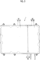
- FIG. 3 is a plan view schematically illustrating the power reception device 1.
- the power reception device 1 includes an accommodation case 50 that accommodates a power reception coil or various elements therein.
- the accommodation case 50 includes a coil accommodation case 51 and a metal case 52.
- the accommodation case 50 includes a case main body 53, a resin lid 54, and a metal lid 55.
- the case main body 53 and the metal lid 55 are formed of a metal such as aluminum, and the resin lid 54 is formed of resin or the like.
- the coil accommodation case 51 is formed of the case main body 53 and the resin lid 54.
- the metal case 52 is formed of the case main body 53 and the metal lid 55.
- FIG. 4 is an exploded perspective view schematically illustrating the power reception device 1. As illustrated in FIG. 4 , an opening portion 53a and an opening portion 53b that open downward are formed in the case main body 53. The opening portion 53a and the opening portion 53b are formed to be arranged in a width direction of the vehicle 2, and the opening portion 53b is formed on the left side of the opening portion 53a.
- the case main body 53 includes a top plate 60, a peripheral wall 61, and an inner-side wall 66.
- the top plate 60 is disposed on the lower surface of the battery case 16.
- the peripheral wall 61 is formed to protrude downward from an outer peripheral edge portion of the top plate 60, and is formed in an annular shape along the outer peripheral edge portion of the top plate 60.
- the peripheral wall 61 includes a front-side wall 62, a rear-side wall 63, a right-outer-side wall 64, and a left-outer-side wall 65.
- the front-side wall 62 is disposed on the front side of the vehicle 2.
- the rear-side wall 63 is disposed on the rear side of the vehicle 2.
- the right-outer-side wall 64 is disposed on the right side of the vehicle 2.
- the left-outer-side wall 65 is disposed on the left side of the vehicle 2.
- the inner-side wall 66 is provided in the annular peripheral wall 61, and is formed to connect the front-side wall 62 and the rear-side wall 63.
- the opening portion 53a is formed by a part of the front-side wall 62, the right-outer-side wall 64, a part of the rear-side wall 63, and the inner-side wall 66.
- the opening portion 53b is formed by a part of the front-side wall 62, the left-outer-side wall 65, a part of the rear-side wall 63, and the inner-side wall 66.
- the resin lid 54 is provided to cover the opening portion 53a. Since the resin lid 54 covers the opening portion 53b, the coil accommodation case 51 that accommodates the power reception coil 40 or the like therein is formed.
- the coil accommodation case 51 is formed by a part of the top plate 60, a part of the front-side wall 62, the inner-side wall 66, a part of the rear-side wall 63, the right-outer-side wall 64, and the resin lid 54.
- the metal lid 55 is provided to cover the opening portion 53b. Since the metal lid 55 covers the opening portion 53b, the metal case 52 that accommodates the power-reception-side electric unit 6 therein is formed.
- the metal case 52 is formed by a part of the top plate 60, a part of the front-side wall 62, the left-outer-side wall 65, a part of the rear-side wall 63, the inner-side wall 66, and the metal lid 55.
- the power reception device 1 includes a metal plate 70 that is formed in a plate shape, and a ferrite plate 71 disposed on a lower surface of the metal plate 70.
- the power reception coil 40 is disposed on a lower surface of the ferrite plate 71, and the power reception coil 40 and the ferrite plate 71 form a coil unit 72.
- the capacitor 41 is disposed on the upper surface side of the metal plate 70.
- the capacitor 41 includes a base plate, and a plurality of ceramic capacitors provided on the base plate.
- the metal plate 70 is disposed between the capacitor 41 and the coil unit 72, and thus the electromagnetic field formed in the vicinity of the power reception coil 40 is prevented from reaching the capacitor 41.
- the power reception coil 40 is a spiral coil.
- the power reception coil 40 is formed by winding a coil wire 40a such that the coil wire 40a surrounds a winding axis O1 extending in an up-down direction.
- the ferrite plate 71 is formed in a plate shape, and the lower surface of the ferrite plate 71 is a coil mounting surface.
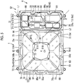
- FIG. 5 is a plan view illustrating the power reception device 1.
- the lower surface (coil mounting surface) of the ferrite plate 71 is viewed in a plan view, in the power reception device 1 from which the resin lid 54 and the metal lid 55 are removed.
- the coil unit 72 is accommodated in the coil accommodation case 51, and the power-reception-side electric unit 6 is accommodated in the metal case 52.
- the metal case 52 is provided to be adjacent to the coil unit 72 and the power reception coil 40.
- the metal case 52 is provided to be adjacent to the coil unit 72 and the power reception coil 40, on the left side (in the width direction) of the vehicle 2.
- the power reception coil 40 is a spiral coil, and the power reception coil 40 is formed in a polygonal shape of which the corners are curved. In an example illustrated in FIG. 5 , the power reception coil 40 is formed in a quadrangle shape.
- the power reception coil 40 includes a plurality of bent sections 73, and straight sections 74, each of which connects the adjacent bent sections 73.
- a hole 77 is formed in the center of the power reception coil 40.
- the ferrite plate 71 includes a plurality of angulated ferrite plates 75a to 75d, and the angulated ferrite plates 75a to 75d are provided to surround the winding axis O1.
- the angulated ferrite plates 75a to 75d are disposed in an annular shape with intervals, and a hole 76 is formed in the center of the ferrite plate 71.
- the angulated ferrite plates 75a, 75b are disposed to be adjacent to the right-outer-side wall 64, and the angulated ferrite plate 75a and the angulated ferrite plate 75c are disposed to be adjacent to the front-side wall 62. Similarly, the angulated ferrite plate 75c and the angulated ferrite plate 75d are disposed to be adjacent to the inner-side wall 66, and the angulated ferrite plate 75b and the angulated ferrite plate 75d are disposed to be adjacent to the rear-side wall 63.
- each of the angulated ferrite plates 75a to 75d is disposed on the upper surface side of the bent sections 73 of the power reception coil 40.
- the angulated ferrite plates 75a to 75d are disposed to radially extend with the winding axis O1 as the center.
- An inner end portion, on the winding axis O1 side, of each of the angulated ferrite plates 75a to 75d is exposed from the hole 77 of the power reception coil 40.
- An outer end portion of each of the angulated ferrite plates 75a to 75d protrudes outward in relation to each bent section 73.
- each of the angulated ferrite plates 75a to 75d includes two split ferrite plates 78.
- the split ferrite plates 78 are disposed with an interval, and a gap 79 is formed between the split ferrite plates 78.
- the gap 79 radially extends with the winding axis O1 as the center.
- a plurality of notches 80a to 80d is formed on the ferrite plate 71.
- the notches 80a to 80d are formed to respectively overlap the straight sections 74 of the power reception coil 40.
- the notches 80a to 80d are formed by the adjacent angulated ferrite plates 75a to 75d.
- the notch 80a is formed between the angulated ferrite plate 75a and the angulated ferrite plate 75b, and the notch 80a is formed at a position adjacent to the right-outer-side wall 64.
- the notch 80b is formed between the angulated ferrite plate 75a and the angulated ferrite plate 75c, and the notch 80b is formed at a position adjacent to the front-side wall 62.
- the notch 80c is formed between the angulated ferrite plate 75c and the angulated ferrite plate 75d, and the notch 80c is formed at a position adjacent to the inner-side wall 66.
- the notch 80d is formed between the angulated ferrite plate 75d and the angulated ferrite plate 75b, and the notch 80d is formed at a position adjacent to the rear-side wall 63.
- each of the notches 80a to 80d in a direction in which the coil wire 40a extends is formed to be increased from an inner peripheral edge portion side to an outer peripheral edge portion side of the power reception coil 40.
- the width of the notch 80c is formed to be increased the more the notch 80c is toward the inner-side wall 66.
- the filter 31 is disposed on the front-side wall 62 in the metal case 52. Specifically, the filter coils 31a, 31b are disposed on the top plate 60, and the capacitors 31c, 31d are disposed below the filter coils 31a, 31b.
- the filter coil 31a and the filter coil 31b are disposed to be arranged in the width direction of the vehicle 2.
- the short-circuit protection circuit 32 and the rectifier 33 are disposed behind the filter 31 in the vehicle 2.
- the short-circuit protection circuit 32 is disposed to be closer to the inner-side wall 66 than the rectifier 33.
- the switching element 44 of the short-circuit protection circuit 32 is provided at a position closer to the inner-side wall 66 than to the left-outer-side wall 65.
- the filter 35 and the sub DC-DC converter 36 are disposed behind the short-circuit protection circuit 32 and the rectifier 33 in the vehicle 2.
- the filter 35 is provided at a position closer to the inner-side wall 66 than the sub DC-DC converter 36. Therefore, the sub DC-DC converter 36 is provided at a position farther from the power reception coil 40 than the filter 35.
- the filter coils 35c, 35d are disposed on the top plate 60, and the capacitors 35a, 35b are disposed below the filter coils 35c, 35d.
- the inner peripheral edge portion of the notch 80c includes a side 81A and a side 81B.
- the side 81A is a side of the angulated ferrite plate 75c
- the side 81B is a side of the angulated ferrite plate 75d.
- a "virtual straight line L1" is an extension line of the side 81A
- a “virtual straight line L2” is an extension line of the side 81B
- An adjacent area R1 is an area interposed between the virtual straight line L1 and the virtual straight line L2.
- the switching element 44 of the short-circuit protection circuit 32 and the switching elements 48 of the sub DC-DC converter 36 are disposed in the adjacent area R1 adjacent to the notch 80c, in the metal case 52. Therefore, it is possible to suppress the exposure of the switching element 44 and the switching elements 48 to an electromagnetic field having high strength, during the power reception.
- the power reception device 1 configured as described above receives electric power from the power transmission device 3 in a non-contact manner, a flux emitted from the power transmission device 3 is linked with the power reception coil 40. Accordingly, an alternating current flows in the power reception coil 40.
- an alternating current flows in the power reception coil 40, an electromagnetic field is formed in the vicinity of the power reception coil 40, and a flux is emitted from the power reception coil 40.
- the flux emitted from the power reception coil 40 is linked with the power transmission coil 28 and returns to the power reception coil 40.
- the power reception coil 40 receives electric power by the flux passing through the power reception coil 40 and the power transmission coil 28.
- a magnetic path MF1 is a path passing through an inner end of the angulated ferrite plate 75c, a portion below the power reception coil 40, an outer peripheral end side of the power reception coil 40, and a portion in the notch 80c.
- a magnetic path MF2 is a path passing through an inner end of the angulated ferrite plate 75c, a portion below the power reception coil 40, an outer end of the angulated ferrite plate 75c, and a portion in the angulated ferrite plate 75c.
- the path length of the magnetic path MF1 passing through the air is longer than the path length of the magnetic path MF2 passing through the air.
- the magnetic resistance of the air is much higher than the magnetic resistance of the ferrite, the magnetic resistance of the magnetic path MF1 is higher than the magnetic resistance of the magnetic path MF2. As a result, the amount of the flux passing through the magnetic path MF1 is smaller than the amount of the flux passing through the magnetic path MF2, and the amount of the flux passing through the magnetic path MF2 is large.
- the distance of the magnetic path MF2 passing through the portion below the power reception coil 40 is longer than that of the magnetic path MF1 passing through the portion below the power reception coil 40, when the flux passing through the magnetic path MF1 is increased, the flux passing through a portion greatly distant from the power reception coil 40 downward is likely to be increased. As a result, the flux linked with the power transmission coil 28 that is positioned below the power reception coil 40 is increased. In this manner, since the notches 80a to 80d are formed on the ferrite plate 71, it is possible to increase the flux linked with the power reception coil 40 and the power transmission coil 28, and thus the coupling coefficient is improved.
- the flux linked with both the power reception coil 40 and the power transmission coil 28 mainly passes through the inner ends of the angulated ferrite plates 75a to 75d, the power transmission coil 28, the outer ends of the angulated ferrite plates 75a to 75d, and portions in the angulated ferrite plates 75a to 75d.
- the power reception coil 40 receives electric power, the amount of the flux passing through the portions in the notches 80a to 80d and a region adjacent to the notches 80a to 80d is small.
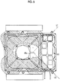
- FIG. 6 is a plan view schematically illustrating a strength distribution of the magnetic field in the vicinity of the power reception coil 40 during the power reception.
- a region indicated by diagonal lines indicates a region in which the strength of the electromagnetic field is high.
- the strength of the electromagnetic field is relatively low in the area interposed between the virtual straight line L1 and the virtual straight line L2 (the adjacent area R1 adjacent to the notch 80c) in the metal case 52.
- all the switching element 44 and the switching elements 48 which are active elements and are provided in the power-reception-side electric unit 6 are disposed in the adjacent area R1 adjacent to the notch 80c.
- at least one of the switching element 44 and the switching elements 48 may be disposed in the adjacent area R1 adjacent to the notch 80c.
- the switching elements 48 of the inverter 45 are disposed at positions closer to the left-outer-side wall 65 than to the inner-side wall 66.
- the strength of the electromagnetic field formed in the vicinity of the power reception coil 40 becomes weak as the distance from the power reception coil 40 is increased. Therefore, even in the adjacent area R1, the strength of the electromagnetic field becomes low as the distance from the power reception coil 40 is increased, and thus it is possible to suppress the exposure of the switching elements 48 to the electromagnetic field having high strength.
- the protection controller 39 and the converter controller 38 are disposed in the adjacent area R1 in the coil accommodation case 51. Therefore, it is possible to suppress the exposure of the protection controller 39 and the converter controller 38 to the electromagnetic field having high strength, during the power reception.
- a current flows in the filter coils 31a, 31b of the filter 31, and a current also flows in the filter coils 35c, 35d.
- the electromagnetic field is formed in the vicinity of the filter coils 31a, 31b and the vicinity of the filter coils 35c, 35d.
- a distance L4 between the converter controller 38 and the filter 31 is longer than a distance L3 between the protection controller 39 and the filter 31. Therefore, the strength of the electromagnetic field to which the converter controller 38 is exposed due to the electromagnetic field formed in the vicinity of the filter 31 is lower than the strength of the electromagnetic field to which the protection controller 39 is exposed.
- a distance L6 between the converter controller 38 and the filter 35 is longer than a distance L5 between the protection controller 39 and the filter 35. Therefore, the strength of the electromagnetic field to which the converter controller 38 is exposed due to the electromagnetic field formed in the vicinity of the filter 35 is lower than the strength of the electromagnetic field to which the protection controller 39 is exposed.
- the strength of the electromagnetic field to which the converter controller 38 is exposed is lower than the strength of the electromagnetic field to which the protection controller 39 is exposed.
- the converter controller 38 is almost usually driven.
- the protection controller 39 is driven when abnormality occurs in the rectifier 33, during the power reception.
- the converter controller 38 has more opportunities of being driven than the protection controller 39. Therefore, in the embodiment, the electromagnetic field to which the converter controller 38 is exposed is reduced, and thereby the protection for the converter controller 38 is achieved.
- FIG. 7 is a plan view illustrating the power transmission device 3.
- the power transmission device 3 includes an accommodation case 100 in which the power transmission unit 24 and the power-transmission-side electric unit 5 are accommodated.
- the accommodation case 100 includes a coil accommodation case 101, and a metal case 102.
- the coil accommodation case 101 includes a case main body 110, and a resin lid 111.
- the metal case 102 includes the case main body 110, and a metal lid 112.
- FIG. 8 is an exploded perspective view illustrating the power transmission device 3.
- the power transmission device 3 includes a ferrite plate 120 on which the power transmission coil 28 is disposed, and a metal plate 122 that is disposed on a lower surface side of the ferrite plate 120.
- the power transmission coil 28 is disposed on an upper surface of the ferrite plate 120, and the upper surface of the ferrite plate 120 is a mounting surface of the power transmission coil 28.
- the power transmission coil 28 and the ferrite plate 120 form a coil unit 121.
- the capacitor 29 is disposed on a lower surface side of the metal plate 122.
- the coil unit 121, the metal plate 122, and the capacitor 29 are accommodated in the coil accommodation case 51.
- the case main body 110 includes a bottom plate 113, a peripheral wall 114, and an inner wall 115.
- the peripheral wall 114 is formed to protrude upward from an outer peripheral edge of the bottom plate 113.
- the peripheral wall 114 includes an outer-side wall 116 that is positioned on the right side of the vehicle, an outer-side wall 117 that is positioned on the left side of the vehicle, an outer-side wall 118 that is positioned on the front side of the vehicle, and an outer-side wall 119 that is positioned on the rear side of the vehicle.
- the inner wall 115 is formed to connect the outer-side wall 116 and the outer-side wall 117.
- An opening portion 123 is formed by a part of the outer-side wall 116, the outer-side wall 118, a part of the outer-side wall 117, and the inner wall 115.
- an opening portion 124 is formed by a part of the outer-side wall 116, the outer-side wall 119, a part of the outer-side wall 117, and the inner wall 115.
- the resin lid 111 covers the opening portion 123, and thereby the coil accommodation case 51 is formed.
- the metal lid 112 covers the opening portion 124, and thereby the metal case 52 is formed.
- FIG. 9 is a plan view illustrating the power transmission device 3.
- FIG. 9 is a plan view in a state where the resin lid 111 and the metal lid 112 are removed from the power transmission device 3.
- the metal case 52 is disposed at a position adjacent to the coil unit 121.
- the power transmission coil 28 includes a plurality of bent sections 125, a pair of long side sections 126, and a pair of short side sections 127.
- the power transmission coil 28 is formed in a hollow shape, and a hole 128 is formed in the center of the power transmission coil 28.
- the power transmission coil 28 is a spiral coil.
- the power transmission coil 28 is formed by winding a coil wire 28a such that the coil wire 28a surrounds a winding axis 02 extending in the up-down direction.
- the ferrite plate 120 includes a plurality of angulated ferrites 130a to 130d, and a plurality of side ferrites 131a, 131b.
- Each of the angulated ferrites 130a to 130d is formed of three split ferrites, and each of the side ferrites 131a, 131b is formed of three split ferrites.
- the angulated ferrites 130a to 130d are disposed below the bent sections 125.
- the side ferrites 131a, 131b are disposed below the long side sections 126.
- An inner end portion of each of the angulated ferrites 130a to 130d and an inner end portion of each of the side ferrites 131a, 131b are positioned inward in relation to the inner peripheral edge portion of the power transmission coil 28.
- An outer end portion of each of the angulated ferrites 130a to 130d and an outer end portion of each of the side ferrites 131a, 131b protrude outward in relation to the outer peripheral edge portion of the power transmission coil 28.
- the angulated ferrites 130a to 130d and the side ferrites 131a, 131b are radially disposed.
- a plurality of notches 132a to 132f is formed on the outer peripheral edge portion of the ferrite plate 120.
- the notches 132a to 132f are formed to respectively overlap the long side sections 126 or the short side sections 127.
- the notches 132a to 132f are formed such that a length of each of the notches 132a to 132f in a direction in which the coil wire 28a extends is increased the more the notches 132a to 132f are toward the outer peripheral edge from the inner peripheral edge of the power transmission coil 28.
- the notch portions 132e, 132f are formed at positions adjacent to the inner wall 115.
- the notch portion 132e is formed between the angulated ferrite 130c and the side ferrite 131b.
- the inner peripheral edge portion of the notch portion 132e includes a side 140 of the angulated ferrite 130c, and a side 141 of the side ferrite 131b.
- the inner peripheral edge portion of the notch portion 132f is formed by a side 142 of the side ferrite 131b, and a side 143 of the angulated ferrite 130d.
- a virtual straight line L10 is an extension line of the side 140
- a virtual straight line L11 is an extension line of the side 141
- a virtual straight line L12 is an extension line of the side 142
- a virtual straight line L13 is an extension line of the side 143.
- An adjacent area R2 adjacent to the notch portion 132e in the metal case 52 is an area interposed between the virtual straight line L10 and the virtual straight line L11 in the metal case 52.
- An adjacent area R3 adjacent to the notch portion 132f in the metal case 52 is an area interposed between the virtual straight line L12 and the virtual straight line L13 in the metal case 52.
- the filter 23 is disposed at a position adjacent to the outer-side wall 116.
- the inverter 22 is disposed to be closer to the outer-side wall 117 than the filter 23.
- the capacitor of the chopper circuit 21 is disposed to be closer to the outer-side wall 117 than the inverter 22.
- the coil of the chopper circuit 21 is disposed to be closer to the outer-side wall 117 than the capacitor.
- the switching element 26 of the chopper circuit 21 is disposed to be closer to the outer-side wall 117 than the coil of the chopper circuit 21, and the switching element 26 is disposed at a position closer to the outer-side wall 119 than to the inner wall 115.
- the rectifier 20 is disposed to be closer to the outer-side wall 117 than the switching element 26 of the chopper circuit 21.
- the switching elements 27a to 27d of the inverter 22 are disposed in the adjacent area R2, and the switching element 26 of the chopper circuit 21 is disposed in the adjacent area R3.
- the power transmission ECU 25 is disposed in the adjacent area R3.
- the power transmission device 3 when the power transmission device 3 transmits power, a current flows in the power transmission coil 28, and an electromagnetic field is formed in the vicinity of the power transmission coil 28.
- the flux linked with both the power transmission coil 28 and the power reception coil 40 mainly passes through the inner end portions of the angulated ferrites 130a to 130d and the side ferrites 131a, 131b, the power reception coil 40, and the outer end portions of the angulated ferrites 130a to 130d and the side ferrites 131a, 131b. That is, the amount of the flux passing through each of the notches 132a to 132f is small, and the strength of the electromagnetic field distributed in each of the notches 132a to 132f is low during the power transmission.
- the switching elements 27a to 27d and the switching element 26 which are active elements of the power-transmission-side electric unit 5 are disposed in the adjacent area R2 or the adjacent area R3.
- the power transmission ECU 25 is also disposed in the adjacent area R3, and thus the exposure of the power transmission ECU 25 to the electromagnetic field having high strength is suppressed.
- the switching element 26 and the power transmission ECU 25 are disposed at positions closer to the outer-side wall 119 than to the inner wall 115, and the distance between the switching element 26 and the power transmission coil 28 is long. Therefore, the strength of the electromagnetic field to which the switching element 26 and the power transmission ECU 25 are exposed is suppressed to be low.
- Embodiment 1 the power reception device and the power transmission device in which the notches are formed in the ferrite plate are described.
- the notches are not essential configurations.
- FIG. 10 is a plan view illustrating a power reception device 1A according to Embodiment 2.
- FIG. 10 illustrates a state in which the resin lid and the metal lid are removed from the power reception device.
- the power reception device 1A includes a ferrite plate 71A, and the ferrite plate 71A is formed in a quadrangle shape.
- the switching elements 48 of the inverter 45 and the converter controller 38 are disposed at positions closer to the left-outer-side wall 65 than to the inner-side wall 66.
- Embodiment 2 since the notch portions are not formed in the ferrite plate 71A, the electromagnetic field is distributed along the outer periphery of the power reception coil 40, and the strength of the electromagnetic field becomes low as the distance from the power reception coil 40 is increased.
- the switching elements 48 of the sub DC-DC converter 36 are disposed at positions closer to the left-outer-side wall 65 than to the inner-side wall 66, and thus the exposure of the switching elements 48 to the electromagnetic field having high strength during the power reception is suppressed.
- the switching element 44 of the short-circuit protection circuit 32 is disposed at a position closer to the inner-side wall 66 than to the left-outer-side wall 65.
- the switching element 44 may be disposed at a position closer to the left-outer-side wall 65 than to the inner-side wall 66.
- At least one of a plurality of active elements provided in the power-reception-side electric unit 6 is disposed at a position closer to the left-outer-side wall 65 than to the inner-side wall 66, and thereby the exposure of the corresponding active element to the electromagnetic field having high strength is suppressed.
- the distance between the converter controller 38 and the filter 31 is longer than the distance between the protection controller 39 and the filter 31, and the exposure of the converter controller 38 to the electromagnetic field having high strength due to the electromagnetic field formed in the vicinity of the filter 31 is suppressed.
- the distance between the converter controller 38 and the filter 35 is longer than the distance between the protection controller 39 and the filter 35, and the exposure of the converter controller 38 to the electromagnetic field having high strength due to the electromagnetic field formed in the vicinity of the filter 35 can be suppressed.
- FIG. 11 is a plan view illustrating the power transmission device 3A according to Embodiment 2.
- the power transmission device 3A includes a ferrite plate 120A that is formed in a plate shape, and the power transmission coil 28 is disposed on an upper surface of the ferrite plate 120A.
- the ferrite plate 120A is formed in a quadrangle shape, and a notch is not formed in an outer peripheral edge of the ferrite plate 120A.
- the switching element 26 of the chopper circuit 21 and the power transmission ECU 25 are disposed at positions closer to the outer-side wall 119 than to the inner wall 115.
- the power transmission device 3A In the power transmission device 3A according to Embodiment 2, during the power transmission, a current flows in the power transmission coil 28, and an electromagnetic field is formed in the vicinity of the power transmission coil 28. Since a notch is not formed in the ferrite plate 120A, the strength of the electromagnetic field formed in the vicinity of the power transmission coil 28 becomes low as the distance from the power transmission coil 28 is increased.
- the switching element 26 and the power transmission ECU 25 are disposed at positions closer to the outer-side wall 119 than to the inner wall 115, it is possible to suppress the exposure of the switching element 26 and the power transmission ECU 25 to the electromagnetic field having high strength due to the electromagnetic field formed in the vicinity of the power transmission coil 28.
- At least one of a plurality of active elements provided in the power-transmission-side electric unit 5 is disposed at a position closer to the outer-side wall 119 than to the inner wall 115, and thereby it is possible to suppress the exposure of the corresponding active element to the electromagnetic field having high strength.
- Embodiments 1 and 2 the power reception devices 1, 1A and the power transmission devices 3, 3A in which a spiral coil is adopted are described. However, various coil types can be adopted.
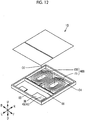
- FIG. 12 is a perspective view illustrating a power reception device 1B in which a DD coil is adopted.
- the power reception device 1B includes a power reception coil 40B.
- the power reception coil 40B includes a unit coil 150, and a unit coil 151 connected to the unit coil 150.
- the unit coil 150 and the unit coil 151 are disposed to be arranged in a front-rear direction of the vehicle.
- the unit coil 150 is formed such that the unit coil 150 surrounds a winding axis 03 extending in the up-down direction from one end of the unit coil 150 to the other end of the unit coil 150.
- the other end of the unit coil 150 is connected to one end of the unit coil 151.
- the unit coil 151 is formed such that the unit coil 151 surrounds a winding axis 04 from the one end to the other end of the unit coil 151.
- the direction of winding the unit coil 150 from the one end to the other end of the unit coil 150 is opposite to the direction of winding the unit coil 151 from the one end to the other end of the unit coil 151.
- the switching elements 48 of the sub DC-DC converter 36 are disposed at positions closer to the left-outer-side wall 65 than to the inner-side wall 66.
- the electromagnetic field formed in the vicinity of the power reception coil 40B is widely distributed in a direction orthogonal to a direction in which the unit coil 150 and the unit coil 151 are arranged.
- the electromagnetic field formed in the vicinity of the power reception coil 40B is widely distributed in the width direction (right-left direction) of the vehicle, and is distributed such that the strength of the electromagnetic field becomes low as the distance from the power reception coil 40B is increased.
- the switching elements 48 of the sub DC-DC converter 36 are disposed at a position close to the left-outer-side wall 65, and the exposure of the switching elements 48 to the electromagnetic field having high strength is suppressed.
- the disclosure can be applied to a power reception device and a power transmission device in which various coils and various ferrite plates are provided.
Landscapes
- Engineering & Computer Science (AREA)
- Power Engineering (AREA)
- Computer Networks & Wireless Communication (AREA)
- Physics & Mathematics (AREA)
- Electromagnetism (AREA)
- Transportation (AREA)
- Mechanical Engineering (AREA)
- Electric Propulsion And Braking For Vehicles (AREA)
- Current-Collector Devices For Electrically Propelled Vehicles (AREA)
- Charge And Discharge Circuits For Batteries Or The Like (AREA)
- Arrangement Or Mounting Of Propulsion Units For Vehicles (AREA)
Abstract
Description
- The disclosure relates to a power reception device and a power transmission device.
- In the related art, various non-contact charging systems in which electric power is transmitted from a power transmission device to a power reception device in a non-contact manner have been proposed (Japanese Unexamined Patent Application Publication No.
2013-154815 JP 2013-154815 A 2013-146154 JP 2013-146154 A 2013-146148 JP 2013-146148 A 2013-110822 JP 2013-110822 A 2013-126327 JP 2013-126327 A - For example, a power reception device described in Japanese Unexamined Patent Application Publication No.
2016-129164 JP 2016-129164 A - A power transmission device includes a spiral power transmission coil, a ferrite plate on which the power transmission coil is disposed, an electrical element, and an accommodation case. In the accommodation case, the electrical element is disposed on a side of the power transmission coil and the ferrite plate in a width direction.
- During electric power transmission, currents flow in the electrical element of the power reception device and the electrical element of power transmission device. When a current flows in each electrical element, noise is emitted from each electrical element.
- In the power reception device and the power transmission device described in
JP 2016-129164 A - Therefore, it has been known that, in a power reception device, a power reception coil and a ferrite plate are accommodated in a coil accommodation case, and an electrical element is accommodated in a metal case adjacent to the coil accommodation case so that the leakage of noise from the electrical element to the outside is suppressed.
- However, in the power reception device in which the electrical element is accommodated in the metal case as described above, during the power reception, an electromagnetic field formed in the vicinity of the power reception coil also enters the metal case, and thus affects an active element of the electrical element. A similar problem arises in the power transmission device.
- The disclosure provides a power reception device which can suppress the influence of the electromagnetic field formed in the vicinity of the power reception coil on the active element of the electrical element provided in the power reception device, during the power reception. In addition, the disclosure provides a power transmission device which can suppress the influence of the electromagnetic field formed in the vicinity of the power transmission coil on the active element of the electrical element provided in the power transmission device, during the power transmission.
- A power reception device according to the disclosure includes a coil; an electric unit; and a metal case. The electric unit is electrically connected to the coil. The metal case is disposed to be adjacent to the coil, and accommodates the electric unit. The electric unit includes at least one active element. The metal case includes an inner-side wall adjacent to the coil, and an outer-side wall that is positioned on the opposite side of the coil from the inner-side wall. The at least one active element is provided at a position closer to the outer-side wall than to the inner-side wall.
- In the power reception device, during the power reception, an electromagnetic field is formed in the vicinity of the power reception coil. Even when the electromagnetic field enters the metal case, since the at least one active element is provided to be closer to the outer-side wall than to the inner-side wall, it is possible to suppress the exposure of the corresponding active element to the electromagnetic field having high strength.
- A power reception device according to the disclosure includes a coil; a ferrite plate; an electric unit; and a metal case. The coil is formed by winding a coil wire, and is formed in a hollow shape. The coil is disposed on the ferrite plate. The electric unit is electrically connected to the coil. The metal case is disposed to be adjacent to the coil, and accommodates the electric unit. The electric unit includes at least one active element. The ferrite plate includes a coil mounting surface on which the coil is disposed. A notch is formed in an outer peripheral edge portion of the ferrite plate. The width of the notch is formed to be increased from an inner peripheral edge portion side of the coil to an outer peripheral edge portion side of the coil. The at least one active element is disposed in an adjacent area that is adjacent to the notch, in the metal case.
- With the power reception device, during the power reception, the flux passing through the notch is small. Therefore, it is possible to suppress the exposure of the active element disposed in the adjacent area that is adjacent to the notch to the electromagnetic field having high strength.
- With the power reception device according to the disclosure, it is possible to suppress the influence of the electromagnetic field formed in the vicinity of the power reception coil on the active element of the electrical element provided in the power reception device, during the power reception. With the power transmission device according to the disclosure and as set forth in claims 4 to 6, it is possible to suppress the influence of the electromagnetic field formed in the vicinity of the power transmission coil on the active element of the electrical element provided in the power transmission device, during the power transmission.
- Features, advantages, and technical and industrial significance of exemplary embodiments of the invention will be described below with reference to the accompanying drawings, in which like numerals denote like elements, and wherein:
-
FIG. 1 is a schematic view schematically illustrating a vehicle including a power reception device, and a power transmission device; -
FIG. 2 is a circuit diagram schematically illustrating a circuit configuration of the power reception device and the power transmission device; -
FIG. 3 is a plan view schematically illustrating the power reception device; -
FIG. 4 is an exploded perspective view schematically illustrating the power reception device; -
FIG. 5 is a plan view illustrating the power reception device and the like; -
FIG. 6 is a plan view schematically illustrating a strength distribution of the magnetic field in the vicinity of a power reception coil during power reception; -
FIG. 7 is a plan view illustrating the power transmission device; -
FIG. 8 is an exploded perspective view illustrating the power transmission device; -
FIG. 9 is a plan view illustrating the power transmission device; -
FIG. 10 is a plan view illustrating a power reception device according toEmbodiment 2; -
FIG. 11 is a plan view illustrating a power transmission device according toEmbodiment 2; and -
FIG. 12 is a perspective view illustrating a power reception device in which a DD coil is adopted. -
Embodiments FIGS. 1 to 12 . In the configurations illustrated inFIGS. 1 to 12 , the same reference numeral is assigned to the same or substantially the same configuration, and the description thereof will not be repeated. InFIGS. 1 to 12 , "F" indicates a front direction of a vehicle; "B" indicates a back direction of a vehicle; "U" indicates an upward direction of a vertical direction; "D" indicates a downward direction of a vertical direction; "L" indicates a left direction of a vehicle; and "R" indicates a right direction of a vehicle. -
FIG. 1 is a schematic view schematically illustrating avehicle 2 including apower reception device 1, and apower transmission device 3. As illustrated inFIG. 1 , thevehicle 2 includes thepower reception device 1, afloor panel 11, abattery pack 12, acushioning member 13, acushioning member 14, and anaccessory battery 15. - The
floor panel 11 is a metallic plate-shaped member that forms abottom surface 10 of thevehicle 2. Thebattery pack 12 includes abattery case 16, and a chargingdevice 17 accommodated in thebattery case 16. For example, thebattery case 16 is formed of a metal such as aluminum. For example, the chargingdevice 17 is a secondary battery or a capacitor which can be charged and discharged. - The
accessory battery 15 is accommodated in an engine compartment of thevehicle 2. As theaccessory battery 15, a lead storage battery or the like can be adopted. - The
power reception device 1 is disposed on a lower surface of thebattery case 16. Thepower reception device 1 receives electric power from thepower transmission device 3 in a non-contact manner, and supplies the electric power to the chargingdevice 17 or theaccessory battery 15. - The cushioning
member 13 and the cushioningmember 14 are provided on the lower surface of thebattery case 16. The cushioningmember 13 is disposed in front of thepower reception device 1, and the cushioningmember 14 is disposed behind thepower reception device 1. Thecushioning members power reception device 1 from a falling object or the like on a road surface. - The
power transmission device 3 is disposed on the ground. Apower supply 19 is connected to thepower transmission device 3. Thepower transmission device 3 supplies electric power supplied from thepower supply 19 to thepower reception device 1 in a non-contact manner. -
FIG. 2 is a circuit diagram schematically illustrating a circuit configuration of thepower reception device 1 and thepower transmission device 3. As illustrated inFIG. 2 , thepower transmission device 3 includes apower transmission unit 24 including apower transmission coil 28, a power-transmission-sideelectric unit 5 that is electrically connected to thepower transmission coil 28, and a power transmission electronic control unit (ECU) 25. - In an example illustrated in
FIG. 2 , the power-transmission-sideelectric unit 5 includes arectifier 20, achopper circuit 21, aninverter 22, and afilter 23. The power-transmission-sideelectric unit 5 includes at least one active element. Specifically, the power-transmission-sideelectric unit 5 includes a switchingelement 26 provided in thechopper circuit 21, and a plurality of switchingelements 27a to 27d provided in theinverter 22. The power-transmission-sideelectric unit 5 is not limited to the above-described electrical elements, and for example, may include a filter in a case where the filter is provided between therectifier 20 and thechopper circuit 21. - The
rectifier 20 is a diode bridge, and includes a plurality of diodes as passive elements. Therectifier 20 performs full-wave rectification on commercial electric power supplied from thepower supply 19, and outputs the rectified electric power to thechopper circuit 21. The electric power output from therectifier 20 is a monopolar pulsating current in which the sinusoidal wave of the commercial electric power is folded at the zero cross point. - The
chopper circuit 21 is a boosting chopper circuit, and includes a coil, the switchingelement 26, a diode, and a capacitor. The switchingelement 26 is an active element, and is a metal-oxide-semiconductor field-effect transistor (MOSFET), for example. A switching operation of the switchingelement 26 is controlled according to a command from thepower transmission ECU 25. - The
chopper circuit 21 functions as a power factor correction (PFC) circuit. Specifically, the switchingelement 26 of thechopper circuit 21 performs switching based on the zero cross point of the full-wave rectified electric power with a frequency sufficiently higher than a frequency of the full-wave rectified electric power supplied from therectifier 20. Accordingly, the conduction interval of a current of the full-wave rectified electric power is widened, and thus the power factor is corrected. Thechopper circuit 21 supplies direct current electric power to theinverter 22. - The
inverter 22 includes theswitching elements 27a to 27d, and diodes which are respectively connected to theswitching elements 27a to 27d in parallel. - The
switching elements 27a to 27d are active elements, and are MOSFETs or Insulated Gate Bipolar Transistors (IGBTs), for example. Theinverter 22 switches theswitching elements 27a to 27d based on an inverter driving signal from thepower transmission ECU 25, and supplies alternating current electric power to thefilter 23. - The
filter 23 includes acapacitor 23a, and filtercoils filter 23 is formed of passive elements. - The
filter 23 removes noise from the alternating current electric power supplied from theinverter 22, and supplies the power to thepower transmission unit 24. Accordingly, it is possible to suppress the emission of electromagnetic interference (EMI) from thepower transmission unit 24. - The
power transmission unit 24 includes thepower transmission coil 28 and acapacitor 29, and thepower transmission unit 24 is formed of passive elements. Thepower transmission coil 28 and thecapacitor 29 are connected in series. Thepower transmission coil 28 and thecapacitor 29 form a serial LC resonator, and the Q factor of thepower transmission unit 24 is equal to or greater than 100. - Alternating current electric power is supplied to the
power transmission unit 24 from thefilter 23. Since the alternating current flows in thepower transmission unit 24, an electromagnetic field is formed in the vicinity of thepower transmission unit 24. - The
power reception device 1 includes apower reception unit 30 including apower reception coil 40, a power-reception-side electric unit 6 that is electrically connected to thepower reception coil 40, and a chargingECU 37. - The power-reception-side electric unit 6 includes a
filter 31, a short-circuit protection circuit 32, arectifier 33, a smoothingcircuit 34, afilter 35, a sub DC-DC converter 36, and anelectric power line 42 and anelectric power line 43 that connect thefilter 31 and therectifier 33. - The charging
ECU 37 includes aconverter controller 38 and aprotection controller 39. Theconverter controller 38 controls the driving of the sub DC-DC converter 36, and theprotection controller 39 controls the driving of the short-circuit protection circuit 32. - The
power reception unit 30 includes thepower reception coil 40 and acapacitor 41, and thepower reception unit 30 is formed of passive elements. Thepower reception coil 40 and thecapacitor 41 form a serial LC resonator, and the Q factor of thepower reception unit 30 is equal to or greater than 100. The resonance frequency of thepower transmission unit 24 is equal to or substantially equal to the resonance frequency of thepower reception unit 30. - The
power reception unit 30 receives electric power through the electromagnetic field formed in the vicinity of thepower transmission unit 24, and thepower reception unit 30 receives electric power from thepower transmission unit 24 in a non-contact manner. The alternating current electric power received by thepower reception unit 30 is supplied to thefilter 31. - The
filter 31 includes a plurality offilter coils capacitors filter 31 is formed of passive elements. - The
filter 31 removes noise from the alternating current electric power supplied from thepower reception unit 30, and supplies the power to the short-circuit protection circuit 32. - The short-
circuit protection circuit 32 includes a switchingelement 44 connected to theelectric power line 42 and theelectric power line 43 that connect thefilter 31 and therectifier 33. The switchingelement 44 is driven according to a control signal from theprotection controller 39. - For example, in a case where the
rectifier 33 or the like is normal, the switchingelement 44 of the short-circuit protection circuit 32 is in an OFF state, and theelectric power line 42 and theelectric power line 43 are in an electrically connected state. - In a case where abnormality is detected in the
rectifier 33 or the like, the switchingelement 44 is turned ON according to the control signal from theprotection controller 39, and electrically connects theelectric power line 42 and theelectric power line 43. Theelectric power line 42 and theelectric power line 43 are electrically connected to form a short circuit, and thus it is possible to prevent the electric power received by thepower reception unit 30 from flowing into therectifier 33. Accordingly, electric power can be prevented from being supplied to therectifier 33 in which abnormality occurs, and it is possible to protect therectifier 33. - The
rectifier 33 includes a plurality ofdiodes 33a to 33d, and therectifier 33 is formed of passive elements. - The
rectifier 33 converts the alternating current electric power that is supplied through the short-circuit protection circuit 32, into direct current electric power, and supplies the direct current electric power to the smoothingcircuit 34. - The smoothing
circuit 34 is formed of a capacitor, and the smoothingcircuit 34 is formed of passive elements. The smoothingcircuit 34 smooths the direct current electric power supplied from therectifier 33 and supplies the power to thefilter 35. - The
filter 35 includes a plurality ofcapacitors 35a, 35b and a plurality offilter coils 35c, 35d, and thefilter 35 is formed of passive elements. Thefilter 35 removes noise from the direct current electric power supplied from the smoothingcircuit 34, and supplies the power to the chargingdevice 17 and the sub DC-DC converter 36. - The sub DC-
DC converter 36 includes aninverter 45, atransformer 46 that is electrically connected to theinverter 45, and arectifier 47 that is electrically connected to thetransformer 46. - The
inverter 45 includes a plurality of switchingelements 48, and a plurality of diodes. The switchingelements 48 are active elements, and are MOSFETs or IGBTs, for example. Theinverter 45 switches the switchingelements 48 ON and OFF based on the driving control signal from theconverter controller 38. Theinverter 45 converts the direct current electric power supplied from thefilter 35 to alternating current electric power. - The
transformer 46 includes two coils, and thetransformer 46 is formed of passive elements. Thetransformer 46 converts (for example, lowers) the voltage of the alternating current electric power supplied from theinverter 45, and supplies the power to therectifier 47. - The
rectifier 47 includes a plurality of diodes, and therectifier 47 is formed of passive elements. Therectifier 47 converts the alternating current electric power supplied from thetransformer 46 into direct current electric power, and supplies the power to theaccessory battery 15. - Next, a configuration of the
power reception device 1 will be described by usingFIG. 3 and the like.FIG. 3 is a plan view schematically illustrating thepower reception device 1. As illustrated inFIG. 3 , thepower reception device 1 includes anaccommodation case 50 that accommodates a power reception coil or various elements therein. - The
accommodation case 50 includes acoil accommodation case 51 and ametal case 52. Theaccommodation case 50 includes a casemain body 53, aresin lid 54, and ametal lid 55. The casemain body 53 and themetal lid 55 are formed of a metal such as aluminum, and theresin lid 54 is formed of resin or the like. - The
coil accommodation case 51 is formed of the casemain body 53 and theresin lid 54. Themetal case 52 is formed of the casemain body 53 and themetal lid 55. -
FIG. 4 is an exploded perspective view schematically illustrating thepower reception device 1. As illustrated inFIG. 4 , anopening portion 53a and anopening portion 53b that open downward are formed in the casemain body 53. Theopening portion 53a and theopening portion 53b are formed to be arranged in a width direction of thevehicle 2, and theopening portion 53b is formed on the left side of theopening portion 53a. - The case
main body 53 includes atop plate 60, aperipheral wall 61, and an inner-side wall 66. Thetop plate 60 is disposed on the lower surface of thebattery case 16. Theperipheral wall 61 is formed to protrude downward from an outer peripheral edge portion of thetop plate 60, and is formed in an annular shape along the outer peripheral edge portion of thetop plate 60. - The
peripheral wall 61 includes a front-side wall 62, a rear-side wall 63, a right-outer-side wall 64, and a left-outer-side wall 65. The front-side wall 62 is disposed on the front side of thevehicle 2. The rear-side wall 63 is disposed on the rear side of thevehicle 2. The right-outer-side wall 64 is disposed on the right side of thevehicle 2. The left-outer-side wall 65 is disposed on the left side of thevehicle 2. - The inner-
side wall 66 is provided in the annularperipheral wall 61, and is formed to connect the front-side wall 62 and the rear-side wall 63. - The
opening portion 53a is formed by a part of the front-side wall 62, the right-outer-side wall 64, a part of the rear-side wall 63, and the inner-side wall 66. Similarly, theopening portion 53b is formed by a part of the front-side wall 62, the left-outer-side wall 65, a part of the rear-side wall 63, and the inner-side wall 66. - The
resin lid 54 is provided to cover theopening portion 53a. Since theresin lid 54 covers theopening portion 53b, thecoil accommodation case 51 that accommodates thepower reception coil 40 or the like therein is formed. - In this manner, the
coil accommodation case 51 is formed by a part of thetop plate 60, a part of the front-side wall 62, the inner-side wall 66, a part of the rear-side wall 63, the right-outer-side wall 64, and theresin lid 54. - The
metal lid 55 is provided to cover theopening portion 53b. Since themetal lid 55 covers theopening portion 53b, themetal case 52 that accommodates the power-reception-side electric unit 6 therein is formed. - In this manner, the
metal case 52 is formed by a part of thetop plate 60, a part of the front-side wall 62, the left-outer-side wall 65, a part of the rear-side wall 63, the inner-side wall 66, and themetal lid 55. - As illustrated in
FIG. 4 , thepower reception device 1 includes ametal plate 70 that is formed in a plate shape, and aferrite plate 71 disposed on a lower surface of themetal plate 70. Thepower reception coil 40 is disposed on a lower surface of theferrite plate 71, and thepower reception coil 40 and theferrite plate 71 form acoil unit 72. Thecapacitor 41 is disposed on the upper surface side of themetal plate 70. - The
capacitor 41 includes a base plate, and a plurality of ceramic capacitors provided on the base plate. Themetal plate 70 is disposed between thecapacitor 41 and thecoil unit 72, and thus the electromagnetic field formed in the vicinity of thepower reception coil 40 is prevented from reaching thecapacitor 41. - The
power reception coil 40 is a spiral coil. Thepower reception coil 40 is formed by winding acoil wire 40a such that thecoil wire 40a surrounds a winding axis O1 extending in an up-down direction. - The
ferrite plate 71 is formed in a plate shape, and the lower surface of theferrite plate 71 is a coil mounting surface. -
FIG. 5 is a plan view illustrating thepower reception device 1. InFIG. 5 , the lower surface (coil mounting surface) of theferrite plate 71 is viewed in a plan view, in thepower reception device 1 from which theresin lid 54 and themetal lid 55 are removed. - As illustrated in
FIG. 5 , thecoil unit 72 is accommodated in thecoil accommodation case 51, and the power-reception-side electric unit 6 is accommodated in themetal case 52. - The
metal case 52 is provided to be adjacent to thecoil unit 72 and thepower reception coil 40. In an example illustrated inFIG. 5 , themetal case 52 is provided to be adjacent to thecoil unit 72 and thepower reception coil 40, on the left side (in the width direction) of thevehicle 2. - Next, a configuration of the
power reception coil 40 and theferrite plate 71 accommodated in thecoil accommodation case 51 will be described. - The
power reception coil 40 is a spiral coil, and thepower reception coil 40 is formed in a polygonal shape of which the corners are curved. In an example illustrated inFIG. 5 , thepower reception coil 40 is formed in a quadrangle shape. - The
power reception coil 40 includes a plurality ofbent sections 73, andstraight sections 74, each of which connects the adjacentbent sections 73. Ahole 77 is formed in the center of thepower reception coil 40. - The
ferrite plate 71 includes a plurality of angulated ferrite plates 75a to 75d, and the angulated ferrite plates 75a to 75d are provided to surround the winding axis O1. The angulated ferrite plates 75a to 75d are disposed in an annular shape with intervals, and ahole 76 is formed in the center of theferrite plate 71. - The angulated
ferrite plates 75a, 75b are disposed to be adjacent to the right-outer-side wall 64, and the angulated ferrite plate 75a and the angulatedferrite plate 75c are disposed to be adjacent to the front-side wall 62. Similarly, the angulatedferrite plate 75c and the angulatedferrite plate 75d are disposed to be adjacent to the inner-side wall 66, and the angulatedferrite plate 75b and the angulatedferrite plate 75d are disposed to be adjacent to the rear-side wall 63. - When the lower surface (coil mounting surface) of the
ferrite plate 71 is seen in a plan view, each of the angulated ferrite plates 75a to 75d is disposed on the upper surface side of thebent sections 73 of thepower reception coil 40. The angulated ferrite plates 75a to 75d are disposed to radially extend with the winding axis O1 as the center. An inner end portion, on the winding axis O1 side, of each of the angulated ferrite plates 75a to 75d is exposed from thehole 77 of thepower reception coil 40. An outer end portion of each of the angulated ferrite plates 75a to 75d protrudes outward in relation to eachbent section 73. - In the example illustrated in
FIG. 5 , each of the angulated ferrite plates 75a to 75d includes two splitferrite plates 78. Thesplit ferrite plates 78 are disposed with an interval, and agap 79 is formed between thesplit ferrite plates 78. Thegap 79 radially extends with the winding axis O1 as the center. - A plurality of
notches 80a to 80d is formed on theferrite plate 71. When thecoil unit 72 is seen in a direction in which the lower surface (coil mounting surface) of theferrite plate 71 is seen in a plan view, thenotches 80a to 80d are formed to respectively overlap thestraight sections 74 of thepower reception coil 40. Thenotches 80a to 80d are formed by the adjacent angulated ferrite plates 75a to 75d. - Specifically, the
notch 80a is formed between the angulated ferrite plate 75a and the angulatedferrite plate 75b, and thenotch 80a is formed at a position adjacent to the right-outer-side wall 64. Thenotch 80b is formed between the angulated ferrite plate 75a and the angulatedferrite plate 75c, and thenotch 80b is formed at a position adjacent to the front-side wall 62. - The
notch 80c is formed between the angulatedferrite plate 75c and the angulatedferrite plate 75d, and thenotch 80c is formed at a position adjacent to the inner-side wall 66. Thenotch 80d is formed between the angulatedferrite plate 75d and the angulatedferrite plate 75b, and thenotch 80d is formed at a position adjacent to the rear-side wall 63. - The width of each of the
notches 80a to 80d in a direction in which thecoil wire 40a extends, is formed to be increased from an inner peripheral edge portion side to an outer peripheral edge portion side of thepower reception coil 40. For example, the width of thenotch 80c is formed to be increased the more thenotch 80c is toward the inner-side wall 66. - Next, mounting positions of the power-reception-side electric unit 6, the
converter controller 38, and theprotection controller 39 that are accommodated in themetal case 52 will be described. - The
filter 31 is disposed on the front-side wall 62 in themetal case 52. Specifically, thefilter coils top plate 60, and thecapacitors filter coils - The
filter coil 31a and thefilter coil 31b are disposed to be arranged in the width direction of thevehicle 2. - The short-
circuit protection circuit 32 and therectifier 33 are disposed behind thefilter 31 in thevehicle 2. The short-circuit protection circuit 32 is disposed to be closer to the inner-side wall 66 than therectifier 33. The switchingelement 44 of the short-circuit protection circuit 32 is provided at a position closer to the inner-side wall 66 than to the left-outer-side wall 65. - The
filter 35 and the sub DC-DC converter 36 are disposed behind the short-circuit protection circuit 32 and therectifier 33 in thevehicle 2. Thefilter 35 is provided at a position closer to the inner-side wall 66 than the sub DC-DC converter 36. Therefore, the sub DC-DC converter 36 is provided at a position farther from thepower reception coil 40 than thefilter 35. - In the
filter 35, the filter coils 35c, 35d are disposed on thetop plate 60, and thecapacitors 35a, 35b are disposed below the filter coils 35c, 35d. - Here, the inner peripheral edge portion of the
notch 80c includes aside 81A and a side 81B. Theside 81A is a side of the angulatedferrite plate 75c, and the side 81B is a side of the angulatedferrite plate 75d. - Here, in
FIG. 5 , a "virtual straight line L1" is an extension line of theside 81A, a "virtual straight line L2" is an extension line of the side 81B. An adjacent area R1 is an area interposed between the virtual straight line L1 and the virtual straight line L2. - Although the details will be described below, in the area that is interposed between the virtual straight line L1 and the virtual straight line L2, and is in the metal case 52 (the adjacent area R1 that is adjacent to the
notch 80c and is in the metal case 52), an electromagnetic field which has relatively low strength is distributed during the power reception. - The switching
element 44 of the short-circuit protection circuit 32 and theswitching elements 48 of the sub DC-DC converter 36 are disposed in the adjacent area R1 adjacent to thenotch 80c, in themetal case 52. Therefore, it is possible to suppress the exposure of the switchingelement 44 and theswitching elements 48 to an electromagnetic field having high strength, during the power reception. - When the
power reception device 1 configured as described above receives electric power from thepower transmission device 3 in a non-contact manner, a flux emitted from thepower transmission device 3 is linked with thepower reception coil 40. Accordingly, an alternating current flows in thepower reception coil 40. When an alternating current flows in thepower reception coil 40, an electromagnetic field is formed in the vicinity of thepower reception coil 40, and a flux is emitted from thepower reception coil 40. The flux emitted from thepower reception coil 40 is linked with thepower transmission coil 28 and returns to thepower reception coil 40. - In this manner, the
power reception coil 40 receives electric power by the flux passing through thepower reception coil 40 and thepower transmission coil 28. - In
FIG. 5 , a magnetic path MF1 is a path passing through an inner end of the angulatedferrite plate 75c, a portion below thepower reception coil 40, an outer peripheral end side of thepower reception coil 40, and a portion in thenotch 80c. - A magnetic path MF2 is a path passing through an inner end of the angulated
ferrite plate 75c, a portion below thepower reception coil 40, an outer end of the angulatedferrite plate 75c, and a portion in the angulatedferrite plate 75c. - Since the magnetic path MF1 passes through a portion in the
notch 80c, the path length of the magnetic path MF1 passing through the air is longer than the path length of the magnetic path MF2 passing through the air. - Since the magnetic resistance of the air is much higher than the magnetic resistance of the ferrite, the magnetic resistance of the magnetic path MF1 is higher than the magnetic resistance of the magnetic path MF2. As a result, the amount of the flux passing through the magnetic path MF1 is smaller than the amount of the flux passing through the magnetic path MF2, and the amount of the flux passing through the magnetic path MF2 is large.
- Since the distance of the magnetic path MF2 passing through the portion below the
power reception coil 40 is longer than that of the magnetic path MF1 passing through the portion below thepower reception coil 40, when the flux passing through the magnetic path MF1 is increased, the flux passing through a portion greatly distant from thepower reception coil 40 downward is likely to be increased. As a result, the flux linked with thepower transmission coil 28 that is positioned below thepower reception coil 40 is increased. In this manner, since thenotches 80a to 80d are formed on theferrite plate 71, it is possible to increase the flux linked with thepower reception coil 40 and thepower transmission coil 28, and thus the coupling coefficient is improved. - The flux linked with both the
power reception coil 40 and thepower transmission coil 28 mainly passes through the inner ends of the angulated ferrite plates 75a to 75d, thepower transmission coil 28, the outer ends of the angulated ferrite plates 75a to 75d, and portions in the angulated ferrite plates 75a to 75d. - Meanwhile, when the
power reception coil 40 receives electric power, the amount of the flux passing through the portions in thenotches 80a to 80d and a region adjacent to thenotches 80a to 80d is small. -
FIG. 6 is a plan view schematically illustrating a strength distribution of the magnetic field in the vicinity of thepower reception coil 40 during the power reception. InFIG. 6 , a region indicated by diagonal lines indicates a region in which the strength of the electromagnetic field is high. As illustrated inFIG. 6 , it can be known that the strength of the electromagnetic field is relatively low in the area interposed between the virtual straight line L1 and the virtual straight line L2 (the adjacent area R1 adjacent to thenotch 80c) in themetal case 52. - In
FIG. 5 , since the switchingelement 44 and theswitching elements 48 are disposed in the adjacent area R1 adjacent to thenotch 80c, it is possible to suppress the exposure of the switchingelements - In the embodiment, all the switching
element 44 and theswitching elements 48 which are active elements and are provided in the power-reception-side electric unit 6 are disposed in the adjacent area R1 adjacent to thenotch 80c. However, at least one of the switchingelement 44 and theswitching elements 48 may be disposed in the adjacent area R1 adjacent to thenotch 80c. - The switching
elements 48 of theinverter 45 are disposed at positions closer to the left-outer-side wall 65 than to the inner-side wall 66. During the power reception, the strength of the electromagnetic field formed in the vicinity of thepower reception coil 40 becomes weak as the distance from thepower reception coil 40 is increased. Therefore, even in the adjacent area R1, the strength of the electromagnetic field becomes low as the distance from thepower reception coil 40 is increased, and thus it is possible to suppress the exposure of the switchingelements 48 to the electromagnetic field having high strength. - The
protection controller 39 and theconverter controller 38 are disposed in the adjacent area R1 in thecoil accommodation case 51. Therefore, it is possible to suppress the exposure of theprotection controller 39 and theconverter controller 38 to the electromagnetic field having high strength, during the power reception. - During the power reception, a current flows in the
filter coils filter 31, and a current also flows in the filter coils 35c, 35d. Thus, the electromagnetic field is formed in the vicinity of thefilter coils - A distance L4 between the
converter controller 38 and thefilter 31 is longer than a distance L3 between theprotection controller 39 and thefilter 31. Therefore, the strength of the electromagnetic field to which theconverter controller 38 is exposed due to the electromagnetic field formed in the vicinity of thefilter 31 is lower than the strength of the electromagnetic field to which theprotection controller 39 is exposed. - A distance L6 between the
converter controller 38 and thefilter 35 is longer than a distance L5 between theprotection controller 39 and thefilter 35. Therefore, the strength of the electromagnetic field to which theconverter controller 38 is exposed due to the electromagnetic field formed in the vicinity of thefilter 35 is lower than the strength of the electromagnetic field to which theprotection controller 39 is exposed. - The strength of the electromagnetic field to which the
converter controller 38 is exposed is lower than the strength of the electromagnetic field to which theprotection controller 39 is exposed. During the power reception, theconverter controller 38 is almost usually driven. Meanwhile, theprotection controller 39 is driven when abnormality occurs in therectifier 33, during the power reception. - In this manner, during the power reception, the
converter controller 38 has more opportunities of being driven than theprotection controller 39. Therefore, in the embodiment, the electromagnetic field to which theconverter controller 38 is exposed is reduced, and thereby the protection for theconverter controller 38 is achieved. - A configuration of the
power transmission device 3 or the like will be described.FIG. 7 is a plan view illustrating thepower transmission device 3. As illustrated inFIG. 7 , thepower transmission device 3 includes anaccommodation case 100 in which thepower transmission unit 24 and the power-transmission-sideelectric unit 5 are accommodated. - The
accommodation case 100 includes acoil accommodation case 101, and ametal case 102. Thecoil accommodation case 101 includes a casemain body 110, and aresin lid 111. Themetal case 102 includes the casemain body 110, and ametal lid 112. -
FIG. 8 is an exploded perspective view illustrating thepower transmission device 3. As illustrated inFIG. 8 , thepower transmission device 3 includes aferrite plate 120 on which thepower transmission coil 28 is disposed, and ametal plate 122 that is disposed on a lower surface side of theferrite plate 120. - The
power transmission coil 28 is disposed on an upper surface of theferrite plate 120, and the upper surface of theferrite plate 120 is a mounting surface of thepower transmission coil 28. Thepower transmission coil 28 and theferrite plate 120 form acoil unit 121. Thecapacitor 29 is disposed on a lower surface side of themetal plate 122. Thecoil unit 121, themetal plate 122, and thecapacitor 29 are accommodated in thecoil accommodation case 51. - The case
main body 110 includes abottom plate 113, aperipheral wall 114, and aninner wall 115. Theperipheral wall 114 is formed to protrude upward from an outer peripheral edge of thebottom plate 113. - The
peripheral wall 114 includes an outer-side wall 116 that is positioned on the right side of the vehicle, an outer-side wall 117 that is positioned on the left side of the vehicle, an outer-side wall 118 that is positioned on the front side of the vehicle, and an outer-side wall 119 that is positioned on the rear side of the vehicle. Theinner wall 115 is formed to connect the outer-side wall 116 and the outer-side wall 117. - An
opening portion 123 is formed by a part of the outer-side wall 116, the outer-side wall 118, a part of the outer-side wall 117, and theinner wall 115. Similarly, anopening portion 124 is formed by a part of the outer-side wall 116, the outer-side wall 119, a part of the outer-side wall 117, and theinner wall 115. - The
resin lid 111 covers theopening portion 123, and thereby thecoil accommodation case 51 is formed. Themetal lid 112 covers theopening portion 124, and thereby themetal case 52 is formed. -
FIG. 9 is a plan view illustrating thepower transmission device 3.FIG. 9 is a plan view in a state where theresin lid 111 and themetal lid 112 are removed from thepower transmission device 3. As illustrated inFIG. 9 , themetal case 52 is disposed at a position adjacent to thecoil unit 121. - The
power transmission coil 28 includes a plurality ofbent sections 125, a pair oflong side sections 126, and a pair ofshort side sections 127. Thepower transmission coil 28 is formed in a hollow shape, and ahole 128 is formed in the center of thepower transmission coil 28. Thepower transmission coil 28 is a spiral coil. Thepower transmission coil 28 is formed by winding acoil wire 28a such that thecoil wire 28a surrounds a windingaxis 02 extending in the up-down direction. - The
ferrite plate 120 includes a plurality of angulatedferrites 130a to 130d, and a plurality ofside ferrites ferrites 130a to 130d is formed of three split ferrites, and each of theside ferrites - When the
ferrite plate 120 and thepower transmission coil 28 are seen in a direction in which the upper surface of theferrite plate 120 is seen in a plan view, the angulatedferrites 130a to 130d are disposed below thebent sections 125. Theside ferrites long side sections 126. - An inner end portion of each of the angulated
ferrites 130a to 130d and an inner end portion of each of theside ferrites power transmission coil 28. An outer end portion of each of the angulatedferrites 130a to 130d and an outer end portion of each of theside ferrites power transmission coil 28. - The angulated
ferrites 130a to 130d and theside ferrites notches 132a to 132f is formed on the outer peripheral edge portion of theferrite plate 120. - When the
ferrite plate 120 and thepower transmission coil 28 are seen in a plan view in a direction in which the upper surface of theferrite plate 120 is seen in a plan view, thenotches 132a to 132f are formed to respectively overlap thelong side sections 126 or theshort side sections 127. - The
notches 132a to 132f are formed such that a length of each of thenotches 132a to 132f in a direction in which thecoil wire 28a extends is increased the more thenotches 132a to 132f are toward the outer peripheral edge from the inner peripheral edge of thepower transmission coil 28. Thenotch portions inner wall 115. - Specifically, the
notch portion 132e is formed between theangulated ferrite 130c and theside ferrite 131b. - The inner peripheral edge portion of the
notch portion 132e includes aside 140 of the angulatedferrite 130c, and aside 141 of theside ferrite 131b. - The inner peripheral edge portion of the
notch portion 132f is formed by aside 142 of theside ferrite 131b, and a side 143 of the angulatedferrite 130d. - In
FIG. 9 , a virtual straight line L10 is an extension line of theside 140, and a virtual straight line L11 is an extension line of theside 141. In addition, a virtual straight line L12 is an extension line of theside 142, and a virtual straight line L13 is an extension line of the side 143. - An adjacent area R2 adjacent to the
notch portion 132e in themetal case 52 is an area interposed between the virtual straight line L10 and the virtual straight line L11 in themetal case 52. An adjacent area R3 adjacent to thenotch portion 132f in themetal case 52 is an area interposed between the virtual straight line L12 and the virtual straight line L13 in themetal case 52. - In the
metal case 52, thefilter 23 is disposed at a position adjacent to the outer-side wall 116. - The
inverter 22 is disposed to be closer to the outer-side wall 117 than thefilter 23. The capacitor of thechopper circuit 21 is disposed to be closer to the outer-side wall 117 than theinverter 22. The coil of thechopper circuit 21 is disposed to be closer to the outer-side wall 117 than the capacitor. The switchingelement 26 of thechopper circuit 21 is disposed to be closer to the outer-side wall 117 than the coil of thechopper circuit 21, and the switchingelement 26 is disposed at a position closer to the outer-side wall 119 than to theinner wall 115. - The
rectifier 20 is disposed to be closer to the outer-side wall 117 than the switchingelement 26 of thechopper circuit 21. - The
switching elements 27a to 27d of theinverter 22 are disposed in the adjacent area R2, and the switchingelement 26 of thechopper circuit 21 is disposed in the adjacent area R3. Thepower transmission ECU 25 is disposed in the adjacent area R3. - In the
power transmission device 3 configured as described above, when thepower transmission device 3 transmits power, a current flows in thepower transmission coil 28, and an electromagnetic field is formed in the vicinity of thepower transmission coil 28. - The flux linked with both the
power transmission coil 28 and thepower reception coil 40 mainly passes through the inner end portions of the angulatedferrites 130a to 130d and theside ferrites power reception coil 40, and the outer end portions of the angulatedferrites 130a to 130d and theside ferrites notches 132a to 132f is small, and the strength of the electromagnetic field distributed in each of thenotches 132a to 132f is low during the power transmission. - In the embodiment, the
switching elements 27a to 27d and the switchingelement 26 which are active elements of the power-transmission-sideelectric unit 5 are disposed in the adjacent area R2 or the adjacent area R3. - Therefore, it is possible to suppress the exposure of the
switching elements 27a to 27d and the switchingelement 26 of the power-transmission-sideelectric unit 5 to the electromagnetic field having high strength, during the power transmission. - The
power transmission ECU 25 is also disposed in the adjacent area R3, and thus the exposure of thepower transmission ECU 25 to the electromagnetic field having high strength is suppressed. - Furthermore, the switching
element 26 and thepower transmission ECU 25 are disposed at positions closer to the outer-side wall 119 than to theinner wall 115, and the distance between the switchingelement 26 and thepower transmission coil 28 is long. Therefore, the strength of the electromagnetic field to which theswitching element 26 and thepower transmission ECU 25 are exposed is suppressed to be low. - In
Embodiment 1, the power reception device and the power transmission device in which the notches are formed in the ferrite plate are described. However, the notches are not essential configurations. -
FIG. 10 is a plan view illustrating a power reception device 1A according toEmbodiment 2.FIG. 10 illustrates a state in which the resin lid and the metal lid are removed from the power reception device. - As illustrated in
FIG. 10 , the power reception device 1A includes aferrite plate 71A, and theferrite plate 71A is formed in a quadrangle shape. - In the embodiment, the switching
elements 48 of theinverter 45 and theconverter controller 38 are disposed at positions closer to the left-outer-side wall 65 than to the inner-side wall 66. - In the power reception device 1A configured as described above, when a reception current flows in the
power reception coil 40 during the power reception, an electromagnetic field is formed in the vicinity of thepower reception coil 40. - In
Embodiment 2, since the notch portions are not formed in theferrite plate 71A, the electromagnetic field is distributed along the outer periphery of thepower reception coil 40, and the strength of the electromagnetic field becomes low as the distance from thepower reception coil 40 is increased. - Meanwhile, the switching
elements 48 of the sub DC-DC converter 36 are disposed at positions closer to the left-outer-side wall 65 than to the inner-side wall 66, and thus the exposure of the switchingelements 48 to the electromagnetic field having high strength during the power reception is suppressed. - In
Embodiment 2, the switchingelement 44 of the short-circuit protection circuit 32 is disposed at a position closer to the inner-side wall 66 than to the left-outer-side wall 65. However, the switchingelement 44 may be disposed at a position closer to the left-outer-side wall 65 than to the inner-side wall 66. - In this manner, in the power reception device 1A according to
Embodiment 2, at least one of a plurality of active elements provided in the power-reception-side electric unit 6 is disposed at a position closer to the left-outer-side wall 65 than to the inner-side wall 66, and thereby the exposure of the corresponding active element to the electromagnetic field having high strength is suppressed. - Similar to
Embodiment 1, also inEmbodiment 2, the distance between theconverter controller 38 and thefilter 31 is longer than the distance between theprotection controller 39 and thefilter 31, and the exposure of theconverter controller 38 to the electromagnetic field having high strength due to the electromagnetic field formed in the vicinity of thefilter 31 is suppressed. In addition, the distance between theconverter controller 38 and thefilter 35 is longer than the distance between theprotection controller 39 and thefilter 35, and the exposure of theconverter controller 38 to the electromagnetic field having high strength due to the electromagnetic field formed in the vicinity of thefilter 35 can be suppressed. - Next, a
power transmission device 3A according toEmbodiment 2 will be described.FIG. 11 is a plan view illustrating thepower transmission device 3A according toEmbodiment 2. As illustrated inFIG. 11 , thepower transmission device 3A includes aferrite plate 120A that is formed in a plate shape, and thepower transmission coil 28 is disposed on an upper surface of theferrite plate 120A. - The
ferrite plate 120A is formed in a quadrangle shape, and a notch is not formed in an outer peripheral edge of theferrite plate 120A. - Various elements of the power-transmission-side
electric unit 5 are accommodated in themetal case 102. The switchingelement 26 of thechopper circuit 21 and thepower transmission ECU 25 are disposed at positions closer to the outer-side wall 119 than to theinner wall 115. - In the
power transmission device 3A according toEmbodiment 2, during the power transmission, a current flows in thepower transmission coil 28, and an electromagnetic field is formed in the vicinity of thepower transmission coil 28. Since a notch is not formed in theferrite plate 120A, the strength of the electromagnetic field formed in the vicinity of thepower transmission coil 28 becomes low as the distance from thepower transmission coil 28 is increased. - In the
power transmission device 3A according toEmbodiment 2, since the switchingelement 26 and thepower transmission ECU 25 are disposed at positions closer to the outer-side wall 119 than to theinner wall 115, it is possible to suppress the exposure of the switchingelement 26 and thepower transmission ECU 25 to the electromagnetic field having high strength due to the electromagnetic field formed in the vicinity of thepower transmission coil 28. - In this manner, in the
power transmission device 3A according toEmbodiment 2, at least one of a plurality of active elements provided in the power-transmission-sideelectric unit 5 is disposed at a position closer to the outer-side wall 119 than to theinner wall 115, and thereby it is possible to suppress the exposure of the corresponding active element to the electromagnetic field having high strength. - In
Embodiments power reception devices 1, 1A and thepower transmission devices -
FIG. 12 is a perspective view illustrating apower reception device 1B in which a DD coil is adopted. As illustrated inFIG. 12 , thepower reception device 1B includes apower reception coil 40B. Thepower reception coil 40B includes aunit coil 150, and aunit coil 151 connected to theunit coil 150. - The
unit coil 150 and theunit coil 151 are disposed to be arranged in a front-rear direction of the vehicle. - Here, the
unit coil 150 is formed such that theunit coil 150 surrounds a windingaxis 03 extending in the up-down direction from one end of theunit coil 150 to the other end of theunit coil 150. - The other end of the
unit coil 150 is connected to one end of theunit coil 151. Theunit coil 151 is formed such that theunit coil 151 surrounds a windingaxis 04 from the one end to the other end of theunit coil 151. - The direction of winding the
unit coil 150 from the one end to the other end of theunit coil 150 is opposite to the direction of winding theunit coil 151 from the one end to the other end of theunit coil 151. - The switching
elements 48 of the sub DC-DC converter 36 are disposed at positions closer to the left-outer-side wall 65 than to the inner-side wall 66. - In the
power reception device 1B, when a current flows in thepower reception coil 40B, the electromagnetic field formed in the vicinity of thepower reception coil 40B is widely distributed in a direction orthogonal to a direction in which theunit coil 150 and theunit coil 151 are arranged. - The electromagnetic field formed in the vicinity of the
power reception coil 40B is widely distributed in the width direction (right-left direction) of the vehicle, and is distributed such that the strength of the electromagnetic field becomes low as the distance from thepower reception coil 40B is increased. - Meanwhile, the switching
elements 48 of the sub DC-DC converter 36 are disposed at a position close to the left-outer-side wall 65, and the exposure of the switchingelements 48 to the electromagnetic field having high strength is suppressed. In this manner, the disclosure can be applied to a power reception device and a power transmission device in which various coils and various ferrite plates are provided. - It should be noted that the embodiments disclosed here are merely examples in all respects, and are not restrictive. The scope of the disclosure is represented by claims not by the above description, and is intended to include the meanings equivalent to the claims and all changes within the scope.
Claims (6)
- A power reception device (1, 1A, 1B) comprising:a coil (40);an electric unit (6) electrically connected to the coil (40); anda metal case (52) disposed to be adjacent to the coil (40), the metal case (52) being configured to accommodate the electric unit (6), whereinthe electric unit (6) includes at least one active element (44, 48),the metal case (52) includes an inner-side wall (66) and an outer-side wall (65),the inner-side wall (66) is adjacent to the coil (40),the outer-side wall (65) is positioned such that the inner-side wall (66) is positioned between the coil (40) and the outer-side wall (65), andthe at least one active element (44, 48) is provided at a position closer to the outer-side wall (65) than to the inner-side wall (66).
- A power reception device (1) comprising:a coil (40) configured by winding a coil wire (40a) in a hollow shape;a ferrite plate (71) on which the coil (40) is disposed;an electric unit (6) electrically connected to the coil (40); anda metal case (52) disposed to be adjacent to the coil (40), the metal case (52) being configured to accommodate the electric unit (6), whereinthe electric unit (6) includes at least one active element (44, 48),the ferrite plate (71) includes a coil mounting surface on which the coil (40) is disposed,a notch (80a, 80b, 80c, 80d) is provided in an outer peripheral edge portion of the ferrite plate (71),a width of the notch (80a, 80b, 80c, 80d) in a direction in which the coil wire (40a) extends increases from an inner peripheral edge portion side of the coil (40) to an outer peripheral edge portion side of the coil, andthe at least one active element (44, 48) is disposed in an adjacent area (R1) that is adjacent to the notch (80c), in the metal case (52).
- The power reception device (1, 1A) according to claim 1 or 2, whereinthe electric unit (6) includesa filter (31) including a filter coil (31a, 31b) connected to the coil (40),a rectifier (33) electrically connected to the filter (31) by a first electric power line (42) and a second electric power line (43),a protection circuit (32) electrically connected to the first electric power line (42) and the second electric power line (43), anda converter (36) electrically connected to the rectifier (33),the protection circuit (32) includesa protection controller (39) configured to control driving of the protection circuit (32) by switching between a state in which the first electric power line (42) and the second electric power line (43) are electrically connected, and a state in which the electric connection between the first electric power line (42) and the second electric power line (43) is cut, anda converter controller (38) configured to control driving of the converter (36), anda distance between the converter controller (38) and the filter coil (31a, 31b) is longer than a distance between the protection controller (39) and the filter coil (31a, 31b).
- A power transmission device (3, 3A) comprising:a coil (28);an electric unit (5) electrically connected to the coil (28); anda metal case (102) disposed to be adjacent to the coil (28), the metal case (102) being configured to accommodate the electric unit (5), whereinthe electric unit (5) includes at least one active element (26, 27a, 27b, 27c, 27d),the metal case includes an inner-side wall (115), and an outer-side wall (119);the inner-side wall (115) is adjacent to the coil (28),the outer-side wall (119) is positioned such that the inner-side wall (115) is positioned between the coil (28) and the outer-side wall (119), andthe at least one active element is provided at a position closer to the outer-side (119) wall than to the inner-side wall (115).
- A power transmission device (3) comprising:a coil (28) configured by winding a coil wire (28a) in a hollow shape;a ferrite plate (120) on which the coil (28) is disposed;an electric unit (5) electrically connected to the coil (28); anda metal case (102) disposed to be adjacent to the coil (28), the metal case (102) being configured to accommodate the electric unit (5), whereinthe electric unit (5) includes at least one active element (26, 27a, 27b, 27c, 27d),the ferrite plate (120) includes a coil mounting surface on which the coil (28) is disposed,a notch (132a-132f) is provided in an outer peripheral edge portion of the ferrite plate (120),a width of the notch (132a-132f) in a direction in which the coil wire (28a) extends increases from an inner peripheral edge portion side of the coil (28) to an outer peripheral edge portion side of the coil (28), andthe at least one active element (26, 27a, 27b, 27c, 27d) is disposed in an adjacent area (R2, R3) that is adjacent to the notch (132e, 132f), in the metal case (102).
- The power transmission device (3, 3A) according to claim 4 or 5, whereinthe electric unit (5) includesa filter (23) including a filter coil (23b, 23c) connected to the coil (28),a rectifier (20) electrically connected to the filter (23) by a first electric power line and a second electric power line,a protection circuit electrically connected to the first electric power line and the second electric power line, anda converter electrically connected to the rectifier (20),the protection circuit includesa protection controller configured to control driving of the protection circuit by switching between a state in which the first electric power line and the second electric power line are electrically connected, and a state in which the electric connection between the first electric power line and the second electric power line is cut, anda converter controller configured to control driving of the converter, anda distance between the converter controller and the filter coil is longer than a distance between the protection controller and the filter coil.
Applications Claiming Priority (1)
| Application Number | Priority Date | Filing Date | Title |
|---|---|---|---|
| JP2016237559A JP6544347B2 (en) | 2016-12-07 | 2016-12-07 | Power receiving device and power transmitting device |
Publications (2)
| Publication Number | Publication Date |
|---|---|
| EP3333861A1 true EP3333861A1 (en) | 2018-06-13 |
| EP3333861B1 EP3333861B1 (en) | 2019-09-25 |
Family
ID=60627450
Family Applications (1)
| Application Number | Title | Priority Date | Filing Date |
|---|---|---|---|
| EP17205559.2A Active EP3333861B1 (en) | 2016-12-07 | 2017-12-05 | Power reception device and power transmission device |
Country Status (4)
| Country | Link |
|---|---|
| US (1) | US10410786B2 (en) |
| EP (1) | EP3333861B1 (en) |
| JP (1) | JP6544347B2 (en) |
| CN (1) | CN108173352B (en) |
Families Citing this family (9)
| Publication number | Priority date | Publication date | Assignee | Title |
|---|---|---|---|---|
| JP6669102B2 (en) * | 2017-03-01 | 2020-03-18 | トヨタ自動車株式会社 | Coil unit |
| DE102017008343B4 (en) * | 2017-09-05 | 2022-07-14 | Patrick Kempka | System for inductive charging of an electric vehicle |
| JP2020080340A (en) * | 2018-11-12 | 2020-05-28 | トヨタ自動車株式会社 | Coil unit |
| CN110182072A (en) * | 2019-05-17 | 2019-08-30 | 嘉兴佰恩智智能科技有限公司 | A kind of wireless charging receiver board |
| JP7356900B2 (en) * | 2019-12-27 | 2023-10-05 | オムロン株式会社 | Resonant oscillation circuit and contactless power supply system |
| DE102020212391A1 (en) * | 2020-09-30 | 2022-03-31 | Mahle International Gmbh | Roadway ceiling panel for an inductive assembly |
| DE112022000573T5 (en) | 2021-04-13 | 2023-10-26 | Ihi Corporation | Coil device |
| JP7853134B2 (en) * | 2022-03-25 | 2026-04-28 | 豊田合成株式会社 | Power transmission equipment |
| US12227093B2 (en) * | 2022-09-01 | 2025-02-18 | Arnold Chase | Conformal charging system |
Citations (8)
| Publication number | Priority date | Publication date | Assignee | Title |
|---|---|---|---|---|
| JP2013110822A (en) | 2011-11-18 | 2013-06-06 | Toyota Motor Corp | Power transmission system, vehicle, and power supply facility |
| JP2013126327A (en) | 2011-12-15 | 2013-06-24 | Toyota Motor Corp | Power receiving apparatus, vehicle including the same, power transmission apparatus, and power transmission system |
| JP2013146154A (en) | 2012-01-16 | 2013-07-25 | Toyota Motor Corp | Power receiving device, power transmitting device, and power transmission system |
| JP2013146148A (en) | 2012-01-16 | 2013-07-25 | Toyota Motor Corp | Vehicle |
| JP2013154815A (en) | 2012-01-31 | 2013-08-15 | Toyota Motor Corp | Vehicle and power transmission system |
| WO2016027570A1 (en) * | 2014-08-20 | 2016-02-25 | トヨタ自動車株式会社 | Power transmission device and method for producing same, and power reception device and method for producing same |
| JP2016129164A (en) | 2015-01-09 | 2016-07-14 | トヨタ自動車株式会社 | Power receiving device and power transmitting device |
| EP3065152A1 (en) * | 2015-03-06 | 2016-09-07 | Brusa Elektronik AG | Primary section of an inductive charger |
Family Cites Families (5)
| Publication number | Priority date | Publication date | Assignee | Title |
|---|---|---|---|---|
| JP4011875B2 (en) * | 2001-09-04 | 2007-11-21 | 富士フイルム株式会社 | Mobile device with built-in image sensor |
| JP2010041906A (en) * | 2008-07-10 | 2010-02-18 | Nec Tokin Corp | Contactless power transmission apparatus, soft magnetic sheet, and module using the same |
| US9653206B2 (en) * | 2012-03-20 | 2017-05-16 | Qualcomm Incorporated | Wireless power charging pad and method of construction |
| JP6232779B2 (en) * | 2013-06-27 | 2017-11-22 | Tdk株式会社 | Coil unit |
| WO2015064473A1 (en) * | 2013-10-28 | 2015-05-07 | 京セラ株式会社 | Control device |
-
2016
- 2016-12-07 JP JP2016237559A patent/JP6544347B2/en active Active
-
2017
- 2017-11-28 CN CN201711210688.6A patent/CN108173352B/en active Active
- 2017-11-29 US US15/826,173 patent/US10410786B2/en active Active
- 2017-12-05 EP EP17205559.2A patent/EP3333861B1/en active Active
Patent Citations (9)
| Publication number | Priority date | Publication date | Assignee | Title |
|---|---|---|---|---|
| JP2013110822A (en) | 2011-11-18 | 2013-06-06 | Toyota Motor Corp | Power transmission system, vehicle, and power supply facility |
| JP2013126327A (en) | 2011-12-15 | 2013-06-24 | Toyota Motor Corp | Power receiving apparatus, vehicle including the same, power transmission apparatus, and power transmission system |
| JP2013146154A (en) | 2012-01-16 | 2013-07-25 | Toyota Motor Corp | Power receiving device, power transmitting device, and power transmission system |
| JP2013146148A (en) | 2012-01-16 | 2013-07-25 | Toyota Motor Corp | Vehicle |
| JP2013154815A (en) | 2012-01-31 | 2013-08-15 | Toyota Motor Corp | Vehicle and power transmission system |
| WO2016027570A1 (en) * | 2014-08-20 | 2016-02-25 | トヨタ自動車株式会社 | Power transmission device and method for producing same, and power reception device and method for producing same |
| EP3185395A1 (en) * | 2014-08-20 | 2017-06-28 | Toyota Jidosha Kabushiki Kaisha | Power transmission device and method for producing same, and power reception device and method for producing same |
| JP2016129164A (en) | 2015-01-09 | 2016-07-14 | トヨタ自動車株式会社 | Power receiving device and power transmitting device |
| EP3065152A1 (en) * | 2015-03-06 | 2016-09-07 | Brusa Elektronik AG | Primary section of an inductive charger |
Also Published As
| Publication number | Publication date |
|---|---|
| US20180158599A1 (en) | 2018-06-07 |
| EP3333861B1 (en) | 2019-09-25 |
| JP6544347B2 (en) | 2019-07-17 |
| US10410786B2 (en) | 2019-09-10 |
| CN108173352A (en) | 2018-06-15 |
| JP2018093690A (en) | 2018-06-14 |
| CN108173352B (en) | 2021-01-12 |
Similar Documents
| Publication | Publication Date | Title |
|---|---|---|
| EP3333861B1 (en) | Power reception device and power transmission device | |
| EP2960910B1 (en) | Power transmission device and power receiving device | |
| KR101717393B1 (en) | Contactless power supply device | |
| CN107925356B (en) | DCDC converter integrated charger | |
| EP3330981A1 (en) | Dual-mode choke coil and high-frequency filter using same, and on-board motor integrated electric power steering and on-board charging device | |
| KR101934018B1 (en) | Power reception apparatus and power transmission apparatus | |
| US9776514B2 (en) | DC-DC converter | |
| US9610847B2 (en) | Power conversion device | |
| US20130021771A1 (en) | Power converter | |
| EP3061643A1 (en) | Vehicle mounting structure of contactless electricity reception device | |
| JP6218150B2 (en) | Power converter | |
| KR20150003894A (en) | Power reception device, power transmission device, and vehicle | |
| KR20150125991A (en) | Contactless power-supply device | |
| JP5715991B2 (en) | Power converter | |
| US10763700B2 (en) | Power transmission device and power reception device | |
| US12151570B2 (en) | Contactless power supply system and coil unit thereof | |
| JP2017079547A (en) | Power converter | |
| KR102180384B1 (en) | Power conversion device | |
| JP6528385B2 (en) | Power converter | |
| US20170170736A1 (en) | Power converter | |
| JP4131352B2 (en) | Step-down DC-DC converter device | |
| JP7003449B2 (en) | In-vehicle device | |
| US10737579B2 (en) | Coil unit | |
| US10622826B2 (en) | Wireless charging unit for an electric vehicle | |
| JP6485318B2 (en) | Power converter and method for manufacturing power converter |
Legal Events
| Date | Code | Title | Description |
|---|---|---|---|
| PUAI | Public reference made under article 153(3) epc to a published international application that has entered the european phase |
Free format text: ORIGINAL CODE: 0009012 |
|
| STAA | Information on the status of an ep patent application or granted ep patent |
Free format text: STATUS: REQUEST FOR EXAMINATION WAS MADE |
|
| 17P | Request for examination filed |
Effective date: 20171205 |
|
| AK | Designated contracting states |
Kind code of ref document: A1 Designated state(s): AL AT BE BG CH CY CZ DE DK EE ES FI FR GB GR HR HU IE IS IT LI LT LU LV MC MK MT NL NO PL PT RO RS SE SI SK SM TR |
|
| AX | Request for extension of the european patent |
Extension state: BA ME |
|
| RIC1 | Information provided on ipc code assigned before grant |
Ipc: H02J 50/70 20160101ALI20190228BHEP Ipc: H01F 27/36 20060101ALI20190228BHEP Ipc: H01F 38/14 20060101ALI20190228BHEP Ipc: H01F 27/40 20060101ALI20190228BHEP Ipc: H01F 27/02 20060101AFI20190228BHEP |
|
| GRAP | Despatch of communication of intention to grant a patent |
Free format text: ORIGINAL CODE: EPIDOSNIGR1 |
|
| STAA | Information on the status of an ep patent application or granted ep patent |
Free format text: STATUS: GRANT OF PATENT IS INTENDED |
|
| INTG | Intention to grant announced |
Effective date: 20190429 |
|
| GRAS | Grant fee paid |
Free format text: ORIGINAL CODE: EPIDOSNIGR3 |
|
| GRAA | (expected) grant |
Free format text: ORIGINAL CODE: 0009210 |
|
| STAA | Information on the status of an ep patent application or granted ep patent |
Free format text: STATUS: THE PATENT HAS BEEN GRANTED |
|
| AK | Designated contracting states |
Kind code of ref document: B1 Designated state(s): AL AT BE BG CH CY CZ DE DK EE ES FI FR GB GR HR HU IE IS IT LI LT LU LV MC MK MT NL NO PL PT RO RS SE SI SK SM TR |
|
| REG | Reference to a national code |
Ref country code: GB Ref legal event code: FG4D |
|
| REG | Reference to a national code |
Ref country code: CH Ref legal event code: EP |
|
| REG | Reference to a national code |
Ref country code: DE Ref legal event code: R096 Ref document number: 602017007303 Country of ref document: DE |
|
| REG | Reference to a national code |
Ref country code: AT Ref legal event code: REF Ref document number: 1184649 Country of ref document: AT Kind code of ref document: T Effective date: 20191015 |
|
| REG | Reference to a national code |
Ref country code: IE Ref legal event code: FG4D |
|
| REG | Reference to a national code |
Ref country code: NL Ref legal event code: MP Effective date: 20190925 |
|
| PG25 | Lapsed in a contracting state [announced via postgrant information from national office to epo] |
Ref country code: SE Free format text: LAPSE BECAUSE OF FAILURE TO SUBMIT A TRANSLATION OF THE DESCRIPTION OR TO PAY THE FEE WITHIN THE PRESCRIBED TIME-LIMIT Effective date: 20190925 Ref country code: BG Free format text: LAPSE BECAUSE OF FAILURE TO SUBMIT A TRANSLATION OF THE DESCRIPTION OR TO PAY THE FEE WITHIN THE PRESCRIBED TIME-LIMIT Effective date: 20191225 Ref country code: HR Free format text: LAPSE BECAUSE OF FAILURE TO SUBMIT A TRANSLATION OF THE DESCRIPTION OR TO PAY THE FEE WITHIN THE PRESCRIBED TIME-LIMIT Effective date: 20190925 Ref country code: FI Free format text: LAPSE BECAUSE OF FAILURE TO SUBMIT A TRANSLATION OF THE DESCRIPTION OR TO PAY THE FEE WITHIN THE PRESCRIBED TIME-LIMIT Effective date: 20190925 Ref country code: NO Free format text: LAPSE BECAUSE OF FAILURE TO SUBMIT A TRANSLATION OF THE DESCRIPTION OR TO PAY THE FEE WITHIN THE PRESCRIBED TIME-LIMIT Effective date: 20191225 Ref country code: LT Free format text: LAPSE BECAUSE OF FAILURE TO SUBMIT A TRANSLATION OF THE DESCRIPTION OR TO PAY THE FEE WITHIN THE PRESCRIBED TIME-LIMIT Effective date: 20190925 |
|
| REG | Reference to a national code |
Ref country code: LT Ref legal event code: MG4D |
|
| PG25 | Lapsed in a contracting state [announced via postgrant information from national office to epo] |
Ref country code: LV Free format text: LAPSE BECAUSE OF FAILURE TO SUBMIT A TRANSLATION OF THE DESCRIPTION OR TO PAY THE FEE WITHIN THE PRESCRIBED TIME-LIMIT Effective date: 20190925 Ref country code: GR Free format text: LAPSE BECAUSE OF FAILURE TO SUBMIT A TRANSLATION OF THE DESCRIPTION OR TO PAY THE FEE WITHIN THE PRESCRIBED TIME-LIMIT Effective date: 20191226 Ref country code: RS Free format text: LAPSE BECAUSE OF FAILURE TO SUBMIT A TRANSLATION OF THE DESCRIPTION OR TO PAY THE FEE WITHIN THE PRESCRIBED TIME-LIMIT Effective date: 20190925 |
|
| REG | Reference to a national code |
Ref country code: DE Ref legal event code: R084 Ref document number: 602017007303 Country of ref document: DE |
|
| REG | Reference to a national code |
Ref country code: AT Ref legal event code: MK05 Ref document number: 1184649 Country of ref document: AT Kind code of ref document: T Effective date: 20190925 |
|
| PG25 | Lapsed in a contracting state [announced via postgrant information from national office to epo] |
Ref country code: ES Free format text: LAPSE BECAUSE OF FAILURE TO SUBMIT A TRANSLATION OF THE DESCRIPTION OR TO PAY THE FEE WITHIN THE PRESCRIBED TIME-LIMIT Effective date: 20190925 Ref country code: AL Free format text: LAPSE BECAUSE OF FAILURE TO SUBMIT A TRANSLATION OF THE DESCRIPTION OR TO PAY THE FEE WITHIN THE PRESCRIBED TIME-LIMIT Effective date: 20190925 Ref country code: PT Free format text: LAPSE BECAUSE OF FAILURE TO SUBMIT A TRANSLATION OF THE DESCRIPTION OR TO PAY THE FEE WITHIN THE PRESCRIBED TIME-LIMIT Effective date: 20200127 Ref country code: PL Free format text: LAPSE BECAUSE OF FAILURE TO SUBMIT A TRANSLATION OF THE DESCRIPTION OR TO PAY THE FEE WITHIN THE PRESCRIBED TIME-LIMIT Effective date: 20190925 Ref country code: NL Free format text: LAPSE BECAUSE OF FAILURE TO SUBMIT A TRANSLATION OF THE DESCRIPTION OR TO PAY THE FEE WITHIN THE PRESCRIBED TIME-LIMIT Effective date: 20190925 Ref country code: IT Free format text: LAPSE BECAUSE OF FAILURE TO SUBMIT A TRANSLATION OF THE DESCRIPTION OR TO PAY THE FEE WITHIN THE PRESCRIBED TIME-LIMIT Effective date: 20190925 Ref country code: RO Free format text: LAPSE BECAUSE OF FAILURE TO SUBMIT A TRANSLATION OF THE DESCRIPTION OR TO PAY THE FEE WITHIN THE PRESCRIBED TIME-LIMIT Effective date: 20190925 Ref country code: EE Free format text: LAPSE BECAUSE OF FAILURE TO SUBMIT A TRANSLATION OF THE DESCRIPTION OR TO PAY THE FEE WITHIN THE PRESCRIBED TIME-LIMIT Effective date: 20190925 Ref country code: AT Free format text: LAPSE BECAUSE OF FAILURE TO SUBMIT A TRANSLATION OF THE DESCRIPTION OR TO PAY THE FEE WITHIN THE PRESCRIBED TIME-LIMIT Effective date: 20190925 |
|
| PG25 | Lapsed in a contracting state [announced via postgrant information from national office to epo] |
Ref country code: SM Free format text: LAPSE BECAUSE OF FAILURE TO SUBMIT A TRANSLATION OF THE DESCRIPTION OR TO PAY THE FEE WITHIN THE PRESCRIBED TIME-LIMIT Effective date: 20190925 Ref country code: CZ Free format text: LAPSE BECAUSE OF FAILURE TO SUBMIT A TRANSLATION OF THE DESCRIPTION OR TO PAY THE FEE WITHIN THE PRESCRIBED TIME-LIMIT Effective date: 20190925 Ref country code: IS Free format text: LAPSE BECAUSE OF FAILURE TO SUBMIT A TRANSLATION OF THE DESCRIPTION OR TO PAY THE FEE WITHIN THE PRESCRIBED TIME-LIMIT Effective date: 20200224 Ref country code: SK Free format text: LAPSE BECAUSE OF FAILURE TO SUBMIT A TRANSLATION OF THE DESCRIPTION OR TO PAY THE FEE WITHIN THE PRESCRIBED TIME-LIMIT Effective date: 20190925 |
|
| REG | Reference to a national code |
Ref country code: DE Ref legal event code: R097 Ref document number: 602017007303 Country of ref document: DE |
|
| PG2D | Information on lapse in contracting state deleted |
Ref country code: IS |
|
| PG25 | Lapsed in a contracting state [announced via postgrant information from national office to epo] |
Ref country code: DK Free format text: LAPSE BECAUSE OF FAILURE TO SUBMIT A TRANSLATION OF THE DESCRIPTION OR TO PAY THE FEE WITHIN THE PRESCRIBED TIME-LIMIT Effective date: 20190925 Ref country code: IS Free format text: LAPSE BECAUSE OF FAILURE TO SUBMIT A TRANSLATION OF THE DESCRIPTION OR TO PAY THE FEE WITHIN THE PRESCRIBED TIME-LIMIT Effective date: 20200126 |
|
| PLBE | No opposition filed within time limit |
Free format text: ORIGINAL CODE: 0009261 |
|
| STAA | Information on the status of an ep patent application or granted ep patent |
Free format text: STATUS: NO OPPOSITION FILED WITHIN TIME LIMIT |
|
| REG | Reference to a national code |
Ref country code: BE Ref legal event code: MM Effective date: 20191231 |
|
| PG25 | Lapsed in a contracting state [announced via postgrant information from national office to epo] |
Ref country code: MC Free format text: LAPSE BECAUSE OF FAILURE TO SUBMIT A TRANSLATION OF THE DESCRIPTION OR TO PAY THE FEE WITHIN THE PRESCRIBED TIME-LIMIT Effective date: 20190925 |
|
| 26N | No opposition filed |
Effective date: 20200626 |
|
| PG25 | Lapsed in a contracting state [announced via postgrant information from national office to epo] |
Ref country code: IE Free format text: LAPSE BECAUSE OF NON-PAYMENT OF DUE FEES Effective date: 20191205 Ref country code: FR Free format text: LAPSE BECAUSE OF NON-PAYMENT OF DUE FEES Effective date: 20191231 Ref country code: LU Free format text: LAPSE BECAUSE OF NON-PAYMENT OF DUE FEES Effective date: 20191205 |
|
| PG25 | Lapsed in a contracting state [announced via postgrant information from national office to epo] |
Ref country code: SI Free format text: LAPSE BECAUSE OF FAILURE TO SUBMIT A TRANSLATION OF THE DESCRIPTION OR TO PAY THE FEE WITHIN THE PRESCRIBED TIME-LIMIT Effective date: 20190925 Ref country code: BE Free format text: LAPSE BECAUSE OF NON-PAYMENT OF DUE FEES Effective date: 20191231 |
|
| PG25 | Lapsed in a contracting state [announced via postgrant information from national office to epo] |
Ref country code: CY Free format text: LAPSE BECAUSE OF FAILURE TO SUBMIT A TRANSLATION OF THE DESCRIPTION OR TO PAY THE FEE WITHIN THE PRESCRIBED TIME-LIMIT Effective date: 20190925 |
|
| PG25 | Lapsed in a contracting state [announced via postgrant information from national office to epo] |
Ref country code: MT Free format text: LAPSE BECAUSE OF FAILURE TO SUBMIT A TRANSLATION OF THE DESCRIPTION OR TO PAY THE FEE WITHIN THE PRESCRIBED TIME-LIMIT Effective date: 20190925 Ref country code: HU Free format text: LAPSE BECAUSE OF FAILURE TO SUBMIT A TRANSLATION OF THE DESCRIPTION OR TO PAY THE FEE WITHIN THE PRESCRIBED TIME-LIMIT; INVALID AB INITIO Effective date: 20171205 |
|
| REG | Reference to a national code |
Ref country code: CH Ref legal event code: PL |
|
| PG25 | Lapsed in a contracting state [announced via postgrant information from national office to epo] |
Ref country code: CH Free format text: LAPSE BECAUSE OF NON-PAYMENT OF DUE FEES Effective date: 20201231 Ref country code: LI Free format text: LAPSE BECAUSE OF NON-PAYMENT OF DUE FEES Effective date: 20201231 |
|
| PG25 | Lapsed in a contracting state [announced via postgrant information from national office to epo] |
Ref country code: TR Free format text: LAPSE BECAUSE OF FAILURE TO SUBMIT A TRANSLATION OF THE DESCRIPTION OR TO PAY THE FEE WITHIN THE PRESCRIBED TIME-LIMIT Effective date: 20190925 |
|
| PG25 | Lapsed in a contracting state [announced via postgrant information from national office to epo] |
Ref country code: MK Free format text: LAPSE BECAUSE OF FAILURE TO SUBMIT A TRANSLATION OF THE DESCRIPTION OR TO PAY THE FEE WITHIN THE PRESCRIBED TIME-LIMIT Effective date: 20190925 |
|
| GBPC | Gb: european patent ceased through non-payment of renewal fee |
Effective date: 20211205 |
|
| PG25 | Lapsed in a contracting state [announced via postgrant information from national office to epo] |
Ref country code: GB Free format text: LAPSE BECAUSE OF NON-PAYMENT OF DUE FEES Effective date: 20211205 |
|
| P01 | Opt-out of the competence of the unified patent court (upc) registered |
Effective date: 20230427 |
|
| PGFP | Annual fee paid to national office [announced via postgrant information from national office to epo] |
Ref country code: DE Payment date: 20251028 Year of fee payment: 9 |