EP3333837A1 - Pixel circuit and drive method therefor, and display panel - Google Patents
Pixel circuit and drive method therefor, and display panel Download PDFInfo
- Publication number
- EP3333837A1 EP3333837A1 EP15900652.7A EP15900652A EP3333837A1 EP 3333837 A1 EP3333837 A1 EP 3333837A1 EP 15900652 A EP15900652 A EP 15900652A EP 3333837 A1 EP3333837 A1 EP 3333837A1
- Authority
- EP
- European Patent Office
- Prior art keywords
- transistor
- driving
- pixel circuit
- voltage
- light
- Prior art date
- Legal status (The legal status is an assumption and is not a legal conclusion. Google has not performed a legal analysis and makes no representation as to the accuracy of the status listed.)
- Granted
Links
Images



Classifications
-
- G—PHYSICS
- G09—EDUCATION; CRYPTOGRAPHY; DISPLAY; ADVERTISING; SEALS
- G09G—ARRANGEMENTS OR CIRCUITS FOR CONTROL OF INDICATING DEVICES USING STATIC MEANS TO PRESENT VARIABLE INFORMATION
- G09G3/00—Control arrangements or circuits, of interest only in connection with visual indicators other than cathode-ray tubes
- G09G3/20—Control arrangements or circuits, of interest only in connection with visual indicators other than cathode-ray tubes for presentation of an assembly of a number of characters, e.g. a page, by composing the assembly by combination of individual elements arranged in a matrix no fixed position being assigned to or needed to be assigned to the individual characters or partial characters
- G09G3/22—Control arrangements or circuits, of interest only in connection with visual indicators other than cathode-ray tubes for presentation of an assembly of a number of characters, e.g. a page, by composing the assembly by combination of individual elements arranged in a matrix no fixed position being assigned to or needed to be assigned to the individual characters or partial characters using controlled light sources
- G09G3/30—Control arrangements or circuits, of interest only in connection with visual indicators other than cathode-ray tubes for presentation of an assembly of a number of characters, e.g. a page, by composing the assembly by combination of individual elements arranged in a matrix no fixed position being assigned to or needed to be assigned to the individual characters or partial characters using controlled light sources using electroluminescent panels
- G09G3/32—Control arrangements or circuits, of interest only in connection with visual indicators other than cathode-ray tubes for presentation of an assembly of a number of characters, e.g. a page, by composing the assembly by combination of individual elements arranged in a matrix no fixed position being assigned to or needed to be assigned to the individual characters or partial characters using controlled light sources using electroluminescent panels semiconductive, e.g. using light-emitting diodes [LED]
- G09G3/3208—Control arrangements or circuits, of interest only in connection with visual indicators other than cathode-ray tubes for presentation of an assembly of a number of characters, e.g. a page, by composing the assembly by combination of individual elements arranged in a matrix no fixed position being assigned to or needed to be assigned to the individual characters or partial characters using controlled light sources using electroluminescent panels semiconductive, e.g. using light-emitting diodes [LED] organic, e.g. using organic light-emitting diodes [OLED]
- G09G3/3225—Control arrangements or circuits, of interest only in connection with visual indicators other than cathode-ray tubes for presentation of an assembly of a number of characters, e.g. a page, by composing the assembly by combination of individual elements arranged in a matrix no fixed position being assigned to or needed to be assigned to the individual characters or partial characters using controlled light sources using electroluminescent panels semiconductive, e.g. using light-emitting diodes [LED] organic, e.g. using organic light-emitting diodes [OLED] using an active matrix
-
- G—PHYSICS
- G09—EDUCATION; CRYPTOGRAPHY; DISPLAY; ADVERTISING; SEALS
- G09G—ARRANGEMENTS OR CIRCUITS FOR CONTROL OF INDICATING DEVICES USING STATIC MEANS TO PRESENT VARIABLE INFORMATION
- G09G3/00—Control arrangements or circuits, of interest only in connection with visual indicators other than cathode-ray tubes
- G09G3/20—Control arrangements or circuits, of interest only in connection with visual indicators other than cathode-ray tubes for presentation of an assembly of a number of characters, e.g. a page, by composing the assembly by combination of individual elements arranged in a matrix no fixed position being assigned to or needed to be assigned to the individual characters or partial characters
- G09G3/22—Control arrangements or circuits, of interest only in connection with visual indicators other than cathode-ray tubes for presentation of an assembly of a number of characters, e.g. a page, by composing the assembly by combination of individual elements arranged in a matrix no fixed position being assigned to or needed to be assigned to the individual characters or partial characters using controlled light sources
- G09G3/30—Control arrangements or circuits, of interest only in connection with visual indicators other than cathode-ray tubes for presentation of an assembly of a number of characters, e.g. a page, by composing the assembly by combination of individual elements arranged in a matrix no fixed position being assigned to or needed to be assigned to the individual characters or partial characters using controlled light sources using electroluminescent panels
- G09G3/32—Control arrangements or circuits, of interest only in connection with visual indicators other than cathode-ray tubes for presentation of an assembly of a number of characters, e.g. a page, by composing the assembly by combination of individual elements arranged in a matrix no fixed position being assigned to or needed to be assigned to the individual characters or partial characters using controlled light sources using electroluminescent panels semiconductive, e.g. using light-emitting diodes [LED]
- G09G3/3208—Control arrangements or circuits, of interest only in connection with visual indicators other than cathode-ray tubes for presentation of an assembly of a number of characters, e.g. a page, by composing the assembly by combination of individual elements arranged in a matrix no fixed position being assigned to or needed to be assigned to the individual characters or partial characters using controlled light sources using electroluminescent panels semiconductive, e.g. using light-emitting diodes [LED] organic, e.g. using organic light-emitting diodes [OLED]
- G09G3/3225—Control arrangements or circuits, of interest only in connection with visual indicators other than cathode-ray tubes for presentation of an assembly of a number of characters, e.g. a page, by composing the assembly by combination of individual elements arranged in a matrix no fixed position being assigned to or needed to be assigned to the individual characters or partial characters using controlled light sources using electroluminescent panels semiconductive, e.g. using light-emitting diodes [LED] organic, e.g. using organic light-emitting diodes [OLED] using an active matrix
- G09G3/3233—Control arrangements or circuits, of interest only in connection with visual indicators other than cathode-ray tubes for presentation of an assembly of a number of characters, e.g. a page, by composing the assembly by combination of individual elements arranged in a matrix no fixed position being assigned to or needed to be assigned to the individual characters or partial characters using controlled light sources using electroluminescent panels semiconductive, e.g. using light-emitting diodes [LED] organic, e.g. using organic light-emitting diodes [OLED] using an active matrix with pixel circuitry controlling the current through the light-emitting element
-
- G—PHYSICS
- G09—EDUCATION; CRYPTOGRAPHY; DISPLAY; ADVERTISING; SEALS
- G09G—ARRANGEMENTS OR CIRCUITS FOR CONTROL OF INDICATING DEVICES USING STATIC MEANS TO PRESENT VARIABLE INFORMATION
- G09G2230/00—Details of flat display driving waveforms
-
- G—PHYSICS
- G09—EDUCATION; CRYPTOGRAPHY; DISPLAY; ADVERTISING; SEALS
- G09G—ARRANGEMENTS OR CIRCUITS FOR CONTROL OF INDICATING DEVICES USING STATIC MEANS TO PRESENT VARIABLE INFORMATION
- G09G2300/00—Aspects of the constitution of display devices
- G09G2300/08—Active matrix structure, i.e. with use of active elements, inclusive of non-linear two terminal elements, in the pixels together with light emitting or modulating elements
- G09G2300/0809—Several active elements per pixel in active matrix panels
- G09G2300/0819—Several active elements per pixel in active matrix panels used for counteracting undesired variations, e.g. feedback or autozeroing
-
- G—PHYSICS
- G09—EDUCATION; CRYPTOGRAPHY; DISPLAY; ADVERTISING; SEALS
- G09G—ARRANGEMENTS OR CIRCUITS FOR CONTROL OF INDICATING DEVICES USING STATIC MEANS TO PRESENT VARIABLE INFORMATION
- G09G2300/00—Aspects of the constitution of display devices
- G09G2300/08—Active matrix structure, i.e. with use of active elements, inclusive of non-linear two terminal elements, in the pixels together with light emitting or modulating elements
- G09G2300/0809—Several active elements per pixel in active matrix panels
- G09G2300/0842—Several active elements per pixel in active matrix panels forming a memory circuit, e.g. a dynamic memory with one capacitor
-
- G—PHYSICS
- G09—EDUCATION; CRYPTOGRAPHY; DISPLAY; ADVERTISING; SEALS
- G09G—ARRANGEMENTS OR CIRCUITS FOR CONTROL OF INDICATING DEVICES USING STATIC MEANS TO PRESENT VARIABLE INFORMATION
- G09G2300/00—Aspects of the constitution of display devices
- G09G2300/08—Active matrix structure, i.e. with use of active elements, inclusive of non-linear two terminal elements, in the pixels together with light emitting or modulating elements
- G09G2300/0809—Several active elements per pixel in active matrix panels
- G09G2300/0842—Several active elements per pixel in active matrix panels forming a memory circuit, e.g. a dynamic memory with one capacitor
- G09G2300/0861—Several active elements per pixel in active matrix panels forming a memory circuit, e.g. a dynamic memory with one capacitor with additional control of the display period without amending the charge stored in a pixel memory, e.g. by means of additional select electrodes
-
- G—PHYSICS
- G09—EDUCATION; CRYPTOGRAPHY; DISPLAY; ADVERTISING; SEALS
- G09G—ARRANGEMENTS OR CIRCUITS FOR CONTROL OF INDICATING DEVICES USING STATIC MEANS TO PRESENT VARIABLE INFORMATION
- G09G2300/00—Aspects of the constitution of display devices
- G09G2300/08—Active matrix structure, i.e. with use of active elements, inclusive of non-linear two terminal elements, in the pixels together with light emitting or modulating elements
- G09G2300/0876—Supplementary capacities in pixels having special driving circuits and electrodes instead of being connected to common electrode or ground; Use of additional capacitively coupled compensation electrodes
-
- G—PHYSICS
- G09—EDUCATION; CRYPTOGRAPHY; DISPLAY; ADVERTISING; SEALS
- G09G—ARRANGEMENTS OR CIRCUITS FOR CONTROL OF INDICATING DEVICES USING STATIC MEANS TO PRESENT VARIABLE INFORMATION
- G09G2320/00—Control of display operating conditions
- G09G2320/02—Improving the quality of display appearance
- G09G2320/0233—Improving the luminance or brightness uniformity across the screen
Definitions
- the present disclosure relates to the field of light emitting display panel, and more particularly, to a pixel circuit capable of compensating a threshold voltage change, a method for driving the pixel circuit and a display panel having the pixel circuit.
- the OLED display panel pixel circuit in the related art includes a driving transistor MD, a transistor M1 functioning as a switch, a capacitor C ST and an organic light-emitting device, i.e., 2T1C.
- the organic light-emitting device includes an organic light-emitting diode D OLED and an inductance capacitor C OLED of the organic light-emitting diode D OLED .
- the transistor M1 is connected to a data signal V DATA and is controlled by a scanning signal V SCAN .
- the driving transistor MD is connected to a pixel power supply V DD and is also connected to the data signal V DATA via the transistor M1.
- Two terminals of the capacitor C ST are connected respectively to the pixel power supply V DD and a node A between the transistor M1 and the driving transistor MD.
- the organic light-emitting diode D OLED and the inductance capacitor C OLED are connected in parallel between the transistor MD and an external power supply V SS .
- the voltage of the external power supply V SS is lower than the voltage of the pixel power supply V DD , for example, the voltage of the external power supply V SS can be the ground voltage.
- I OLED is the current flowing through the organic light-emitting device.
- V GS is a voltage applied between the gate electrode and the source electrode of the driving transistor MD, and V GS is determined by a voltage across the C ST .
- V TH is a threshold voltage of the driving transistor MD.
- ⁇ is a gain factor of the driving transistor MD, which is determined by a size of the device and a carrier mobility of a semi-conductor. It can be seen from formula, the current flowing through the organic light-emitting device may be affected by the threshold voltage of the driving transistor MD. Since the threshold voltage of each transistor in the organic light-emitting display panel may be different from each other in a production process, as well as an electron mobility of each transistor. On this basis, the current I OLED generated in the circuit is variable even given the same V GS , thereby resulting non-uniformity of brightness.
- embodiments of the present disclosure provide a pixel circuit, in which the influence of a change of a threshold voltage on brightness may be reduced.
- a pixel circuit including a light-emitting diode; a driving transistor; a first transistor connected between a data line and the driving transistor, a gate electrode of the first transistor being connected to a first scanning line; a second transistor connected between a first power line and the driving transistor, and a gate electrode of the second transistor being connected to a second scanning line; a third transistor connected between a gate electrode of the driving transistor and the second transistor, a gate electrode of the third transistor being connected to a third scanning line; and a driving capacitor connected between the gate electrode of the driving transistor and the first power line; in which, the driving transistor is further connected to a second power line via the light-emitting diode.
- a display panel including a plurality of pixel circuits described above arranged in an array; a scan driving unit, configured to provide scanning signals to the first scanning line, the second scanning line and the third scanning line respectively; a data driving unit, configured to provide a data signal to a data line; a first power supply, configured to provide a first voltage to the first power line; and a second power supply, configured to provide a second voltage to the second power line.
- a method for driving a pixel circuit is provided, the method is applied in a pixel circuit as described above, and the driving transistor has a threshold voltage.
- the method includes: conducting the first transistor, the second transistor, the third transistor and the driving transistor, such that potentials at both ends of the driving capacitor are the first voltage provided by the first power line; conducting the first transistor, the third transistor and the driving transistor, and cutting off the second transistor, such that a data voltage is output by the data line to the driving transistor via the first transistor, the driving capacitor discharges electricity to the data line via the third transistor, the driving transistor and the first transistor in turn until a potential of an end of the driving capacitor connected to the driving transistor being the sum of the data voltage and the threshold voltage; and conducting the second transistor, and cutting off the first transistor and the third transistor, such that the driving transistor is driven to be conducted by the driving capacitor, and a light-emitting element is driven to emit light by the first voltage provided by the first power line.
- the current flowing through the light-emitting element is only related to the data signal provided by the data line, such that the influence of the change of the threshold voltage on the current flowing through the light-emitting element is reduced.
- a display panel 8 includes a scan driving unit 10, a data driving unit 20, a transmitting control driving unit 30, a display unit 40, a first power supply 50 and a second power supply 60.
- the display unit 40 includes a plurality of pixel circuits 70 arranged in a matrix.
- the scan driving unit 10, the data driving unit 20 and the transmitting control driving unit 30 are configured to provide a scanning signal V SCAN (including a first scanning signal V SCAN1 , a second scanning signal V SCAN2 and a third scanning signal V SCAN3 ), a data signal V DATA and an emitting control signal V EM to each pixel circuit 70, respectively.
- the first power supply 50, the second power supply 60 are configured to provide a first voltage V DD and a second voltage V SS to each pixel circuit 70, respectively.
- the pixel 70 has a first scanning line configured to transmit a first scanning signal V SCAN1 , a second scanning line configured to transmit a second scanning signal V SCAN2 , a third scanning line configured to transmit a third scanning signal V SCAN3 , a first power supply configured to provide a first voltage V DD , a second power supply configured to provide a second voltage V SS , a data line configured to transmit a data signal V DATA , and an emission line configured to transmit the emitting control signal V EM .
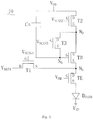
- the pixel circuit 70 includes: a driving transistor TD; a light-emitting diode D OLED , an electrode of the light-emitting diode D OLED being connected to the second power line; a first transistor T1, a control electrode of the first transistor T1 being connected to the first scanning line, and two controlled electrodes of the first transistor T1 being connected to the data line and a first controlled electrode of the driving transistor TD respectively; a second transistor T2, a control electrode of the second transistor T2 being connected to the second scanning line, and two controlled electrodes of the second transistor T2 being connected to the first power line and a second controlled electrode of the driving transistor TD respectively; a third transistor T3, a control electrode of the third transistor T3 being connected to the third scanning line, and two controlled electrodes of the third transistor T3 being connected to a control electrode and the second controlled electrode of the driving transistor TD respectively; an emitting transistor TE, a control electrode of the emitting transistor TE being connected to the emission line, and two controlled electrodes of the emitting transistor
- an organic light-emitting diode is an example of the light-emitting element.
- the present disclosure is not limited to such an example, the light-emitting element may also be an inorganic light-emitting diode.
- the driving transistor TD, the first transistor T1, the second transistor T2, the third transistor T3 and the emitting transistor TE are preferably thin-film field-effect transistors, and are specifically N-type thin-film field-effect transistors, but are not limited thereto, which may also be P-type thin-film field-effect transistors or other electronic devices capable of realizing switching functions, such as a triode.
- a voltage value of the second voltage V SS is lower than a voltage value of the first voltage V DD , such as a ground voltage.
- the driving transistor TD includes a control electrode and two controlled electrodes controlled to be conducted or non-conducted by the control electrode, in which, the control electrode is a gate electrode G of the driving transistor TD, and the two controlled electrodes are a drain electrode D and a source electrode S.
- the first transistor T1, the second transistor T2, the third transistor T3 and the emitting transistor TE are in the same way as the driving transistor TD.
- a drain electrode D and a source electrode S of the first transistor T1 are connected to the data line and a source electrode S of the driving transistor TD respectively, and a gate electrode G of the first transistor T1 is connected to the first scanning line.
- a drain electrode D and a source electrode S of the second transistor T2 are connected to the first power line and the drain electrode D of the driving transistor TD respectively, and a gate electrode G of the second transistor is connected to the second scanning line.
- a drain electrode D and a source electrode S of the third transistor T3 are connected to the source electrode S of the second transistor T2 and gate electrode G of the driving transistor TD respectively, and the gate electrode G of the third transistor T3 is connected to the third scanning line.
- a drain electrode D of the emitting transistor TE is connected to the source electrode S of the driving transistor TD, and a source electrode S of the emitting transistor TE is connected to the second power line via the light-emitting diode D OLED .
- a cathode of the light-emitting diode D OLED is connected to the second power line, and a gate electrode G of the emitting transistor TE is connected to the emission line.
- a node that connecting the first transistor T1, the driving transistor TD and the emitting transistor TE is defined as N G
- the driving transistor TD and the third transistor T3 is defined as N D
- a node that connecting the driving capacitor C ST , the third transistor T3 and the driving transistor TD is defined as N G .
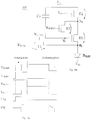
- the pixel circuit 70 in Fig. 3 is configured to be operating according to a timing diagram of an embodiment illustrated in Fig. 4a .
- each operating cycle of the pixel circuit 70 can be divided into four phases.
- a first phase i.e., a charging phase
- an operating condition of the pixel circuit 70 is illustrated in Fig. 4b .
- voltages of the node N D and the node N G are charged to be voltage of the first voltage V DD .
- the first scanning signal V SCAN1 and the emitting control signal V EM are low level signals
- the second scanning signal V SCAN2 and the third scanning signal V SCAN3 are high level signals.
- the first transistor T1 and the emitting transistor TE are turned off, and the second transistors T2 and the third transistor T3 are conducted.
- the first voltage V DD is transmitted to the node N G via the second transistor T2 and the third transistor T3, i.e., both the node N G and the node N D are charged to be the first voltage V DD .
- the driving transistor TD is also turned off under such a condition.
- the data signal V DATA may be a low level signal at this phase.
- the node N D and N G are charged to be the sum of voltages of the data signal V DATA and the threshold voltage V TH of the driving transistor TD, and the node N S is charged to be the voltage of the data signal V DATA .
- the second scanning signal V SCAN2 and the emitting control signal V EM are low level signals
- the first scanning signal V SCAN1 and the third scanning signal V SCAN3 are high level signals.
- a voltage difference between a voltage of the first scanning signal V SCAN1 and a voltage of the data signal V DATA is higher than a threshold voltage of the first transistor T1 and a voltage difference between a voltage of the first voltage V DD and a voltage of the data signal V DATA is higher than a threshold voltage of the driving transistor TD.
- V GS of the first transistor T1 is higher than V TH of the first transistor T1, and the first transistor T1 is conducted.
- the potential of the node N S is the voltage value of the data signal V DATA .
- the driving transistor TD is conducted, and the potential of the node N D is also the voltage value of the data signal V DATA .
- the third transistor T3 is conducted, an end of the driving capacitor C ST , being connected to the third transistor T3, discharges electricity to the data line through the third transistors T3, the driving transistor TD and the first transistor T1 in turn, and the potential of the driving capacitor is gradually reduced.
- the V GS of the driving transistor TD is equal to V TH of the driving transistor TD, and in this case, the driving transistor TD is turned off.
- voltages of the node N D and N G remain at (V DATA + V TH ), and the potential of node N S is equal to the voltage value of the data signal V DATA .
- a third phase i.e., an emitting phase
- the second transistor T2 the driving transistor TD and the emitting transistor TE are conducted, and the light-emitting diode D OLED emits light.
- an operating condition of the pixel circuit 70 at the emitting phase is illustrated in Fig. 6b .
- the second scanning signal V SCAN2 and the emitting control signal V EM are high level signals
- the third scanning signal V SCAN3 and the first scanning signal V SCAN1 are low level signals.
- the second transistor T2 and the emitting transistor TE are turned on, and the first transistor T1 and the third transistor T3 are cut off.
- the driving transistor TD is conducted by the power stored in the driving capacitor C ST , and a current generated by the first voltage V DD flows through the light-emitting diode D OLED to emit light.
- the driving capacitor C ST discharges electricity to the second power line.
- a fourth phase i.e., a discharging phase
- an operating condition of the pixel circuit 70 is illustrated in Fig. 7b .
- the emitting control signal V EM is a high level signal
- the first scanning signal V SCAN1 , the second scanning signal V SCAN2 and the third scanning signal V SCAN3 are low level signals.
- the emitting transistor TE is conducted, and since the potential of the node N G is still remained at (V DATA +V TH ), the driving transistor TD is also conducted and the first transistor T1, the second transistor T2 and the third transistor T3 are turned off.
- the light-emitting diode D OLED is conducted at original potential, so that potentials of the node N D and the node N S are gradually reduced along with the second voltage V SS . In this way, a case that the data voltage is written slowly or even unable to be written in a next compensating phase when the data voltage of the next cycle is too low (i.e., the data voltage is lower than the voltage of the node N S ) may be avoided. Therefore, a response speed is improved, as well as a display effect.
- a schematic diagram of another pixel circuit 70' is provided.
- the difference between the pixel circuit 70' and the pixel circuit 70 of the above embodiments lies in that the emitting transistor TE is omitted in the pixel circuit 70', and thus the driving transistor TD is directly connected to the light-emitting diode D OLED .
- a driving timing diagram of the pixel circuit 70' is illustrated in Fig. 10a .
- the voltage of the node N S is charged to the voltage of the data signal V DATA
- voltages of the node N D and the node N G are charged to the voltage of the first voltage V DD .
- the first scanning signal V SCAN1 , the second scanning signal V SCAN2 and the third scanning signal V SCAN3 are high level signals.
- the first transistor T1, the second transistor T2 and the third transistor T3 are conducted, and the driving transistor TD is conducted accordingly.
- the first voltage V DD is transmitted to the node N G through the second transistor T2 and the third transistor T3, i.e., both the node N G and the node N D are charged to be a voltage as the first voltage V DD .
- the first transistor T1 is conducted, and the potential of the node N S is the voltage of the data signal V DATA .
- the node N D and N G are charged to (V DATA + V TH ), and the node N S is charged to the voltage of data signal V DATA .
- a third phase i.e., an emitting phase, both the second transistor T2 and the driving transistor TD are conducted, and the light-emitting diode D OLED emits light.
- the operating principles and the operating processes are the same as those of the pixel circuit 70 in the above embodiments, which are not described in detail here.
- a discharging phase may also be included after the third phase in the timing diagram, the operating mode and principle are the same as those of described above, which are not described in detail here.
Landscapes
- Engineering & Computer Science (AREA)
- Physics & Mathematics (AREA)
- Computer Hardware Design (AREA)
- General Physics & Mathematics (AREA)
- Theoretical Computer Science (AREA)
- Control Of Indicators Other Than Cathode Ray Tubes (AREA)
- Control Of El Displays (AREA)
- Electroluminescent Light Sources (AREA)
Abstract
Description
- The present disclosure relates to the field of light emitting display panel, and more particularly, to a pixel circuit capable of compensating a threshold voltage change, a method for driving the pixel circuit and a display panel having the pixel circuit.
- As a current mode light-emitting device, an organic light-emitting diode (OLED for short) has been increasingly applied in high-performance organic light-emitting display panels. Referring to
Fig, 1 , the OLED display panel pixel circuit in the related art includes a driving transistor MD, a transistor M1 functioning as a switch, a capacitor CST and an organic light-emitting device, i.e., 2T1C. The organic light-emitting device includes an organic light-emitting diode DOLED and an inductance capacitor COLED of the organic light-emitting diode DOLED. The transistor M1 is connected to a data signal VDATA and is controlled by a scanning signal VSCAN. The driving transistor MD is connected to a pixel power supply VDD and is also connected to the data signal VDATA via the transistor M1. Two terminals of the capacitor CST are connected respectively to the pixel power supply VDD and a node A between the transistor M1 and the driving transistor MD. The organic light-emitting diode DOLED and the inductance capacitor COLED are connected in parallel between the transistor MD and an external power supply VSS. The voltage of the external power supply VSS is lower than the voltage of the pixel power supply VDD, for example, the voltage of the external power supply VSS can be the ground voltage. When a gate electrode of the transistor M1 responds to scanning signal VSCAN and conducts the transistor M1, the capacitor CST is charged based on the data signal VDATA, and then the voltage in the capacitor CST is applied on the gate electrode of the driving transistor MD, thereby conducting the driving transistor MD, so that the organic light-emitting device through which current flows emits light. - The current provided to the organic light-emitting device through the driving transistor MD can be calculated by following formula:

- IOLED is the current flowing through the organic light-emitting device. VGS is a voltage applied between the gate electrode and the source electrode of the driving transistor MD, and VGS is determined by a voltage across the CST. VTH is a threshold voltage of the driving transistor MD. β is a gain factor of the driving transistor MD, which is determined by a size of the device and a carrier mobility of a semi-conductor. It can be seen from formula, the current flowing through the organic light-emitting device may be affected by the threshold voltage of the driving transistor MD. Since the threshold voltage of each transistor in the organic light-emitting display panel may be different from each other in a production process, as well as an electron mobility of each transistor. On this basis, the current IOLED generated in the circuit is variable even given the same VGS, thereby resulting non-uniformity of brightness.
- Accordingly, embodiments of the present disclosure provide a pixel circuit, in which the influence of a change of a threshold voltage on brightness may be reduced.
- In embodiments of the present disclosure, a pixel circuit is provided, including a light-emitting diode; a driving transistor; a first transistor connected between a data line and the driving transistor, a gate electrode of the first transistor being connected to a first scanning line; a second transistor connected between a first power line and the driving transistor, and a gate electrode of the second transistor being connected to a second scanning line; a third transistor connected between a gate electrode of the driving transistor and the second transistor, a gate electrode of the third transistor being connected to a third scanning line; and a driving capacitor connected between the gate electrode of the driving transistor and the first power line; in which, the driving transistor is further connected to a second power line via the light-emitting diode.
- In embodiments of the present disclosure, a display panel is provided, including a plurality of pixel circuits described above arranged in an array; a scan driving unit, configured to provide scanning signals to the first scanning line, the second scanning line and the third scanning line respectively; a data driving unit, configured to provide a data signal to a data line; a first power supply, configured to provide a first voltage to the first power line; and a second power supply, configured to provide a second voltage to the second power line.
- In embodiments of the present disclosure, a method for driving a pixel circuit is provided, the method is applied in a pixel circuit as described above, and the driving transistor has a threshold voltage. The method includes: conducting the first transistor, the second transistor, the third transistor and the driving transistor, such that potentials at both ends of the driving capacitor are the first voltage provided by the first power line; conducting the first transistor, the third transistor and the driving transistor, and cutting off the second transistor, such that a data voltage is output by the data line to the driving transistor via the first transistor, the driving capacitor discharges electricity to the data line via the third transistor, the driving transistor and the first transistor in turn until a potential of an end of the driving capacitor connected to the driving transistor being the sum of the data voltage and the threshold voltage; and conducting the second transistor, and cutting off the first transistor and the third transistor, such that the driving transistor is driven to be conducted by the driving capacitor, and a light-emitting element is driven to emit light by the first voltage provided by the first power line.
- With the pixel circuit, the display panel and the method for driving the pixel circuit of the present disclosure, the current flowing through the light-emitting element is only related to the data signal provided by the data line, such that the influence of the change of the threshold voltage on the current flowing through the light-emitting element is reduced.
- The following drawings are intended to illustrate embodiments of the present disclosure in detail with reference to specific embodiments. It should be understood that, elements illustrated in drawings are not representative of actual size and ratio relationships and are merely illustrative, and should not to be construed as a limitation of the present disclosure.
-
Fig. 1 is a schematic diagram of a pixel circuit in the related art. -
Fig. 2 is a schematic diagram of a display panel according to an embodiment of the present disclosure. -
Fig. 3 is a schematic diagram of a pixel circuit of a display panel inFig. 2 according to an embodiment of the present disclosure. -
Fig. 4a is a timing diagram of a pixel circuit inFig. 3 , andFig. 4b is a schematic diagram of a pixel circuit inFig. 3 at a charging phase of the timing diagram. -
Fig. 5a is a timing diagram of a pixel circuit inFig. 3 , andFig. 5b is a schematic diagram of a pixel circuit inFig. 3 at a compensating phase of the timing diagram. -
Fig. 6a is a timing diagram of a pixel circuit inFig. 3 , andFig. 6b is a schematic diagram of a pixel circuit inFig. 3 at an emitting phase of the timing diagram. -
Fig. 7a is a timing diagram of a pixel circuit inFig. 3 , andFig. 7b is a schematic diagram of a pixel circuit inFig. 3 at a discharging phase of the timing diagram. -
Fig. 8 is a schematic diagram illustrating a relationship between a threshold voltage of the driving transistor of the pixel circuit inFig. 3 and a change of a current. -
Fig. 9 is a schematic diagram of a pixel circuit of a display panel inFig. 2 according to another embodiment of the present disclosure. -
Fig. 10a is a timing diagram of a pixel circuit inFig. 9 , andFig. 10b is a schematic diagram of a pixel circuit inFig. 9 at a charging phase of the timing diagram. - In order to make purposes, technical solutions and advantages of embodiments of the present disclosure more clear, reference will be made in detail to embodiments of the present disclosure with accompanying drawings. It should be understood that, the embodiments described herein according to drawings are explanatory and illustrative, and are not construed to limit the present disclosure.
- Referring to
Fig. 2 , a display panel 8 includes ascan driving unit 10, adata driving unit 20, a transmittingcontrol driving unit 30, adisplay unit 40, afirst power supply 50 and asecond power supply 60. Thedisplay unit 40 includes a plurality ofpixel circuits 70 arranged in a matrix. Thescan driving unit 10, thedata driving unit 20 and the transmittingcontrol driving unit 30 are configured to provide a scanning signal VSCAN (including a first scanning signal VSCAN1, a second scanning signal VSCAN2 and a third scanning signal VSCAN3), a data signal VDATA and an emitting control signal VEM to eachpixel circuit 70, respectively. Thefirst power supply 50, thesecond power supply 60 are configured to provide a first voltage VDD and a second voltage VSS to eachpixel circuit 70, respectively. - Referring to
Fig. 3 , in an embodiment of the present disclosure, thepixel 70 has a first scanning line configured to transmit a first scanning signal VSCAN1, a second scanning line configured to transmit a second scanning signal VSCAN2, a third scanning line configured to transmit a third scanning signal VSCAN3, a first power supply configured to provide a first voltage VDD, a second power supply configured to provide a second voltage VSS, a data line configured to transmit a data signal VDATA, and an emission line configured to transmit the emitting control signal VEM. - Further, the
pixel circuit 70 includes: a driving transistor TD; a light-emitting diode DOLED, an electrode of the light-emitting diode DOLED being connected to the second power line; a first transistor T1, a control electrode of the first transistor T1 being connected to the first scanning line, and two controlled electrodes of the first transistor T1 being connected to the data line and a first controlled electrode of the driving transistor TD respectively; a second transistor T2, a control electrode of the second transistor T2 being connected to the second scanning line, and two controlled electrodes of the second transistor T2 being connected to the first power line and a second controlled electrode of the driving transistor TD respectively; a third transistor T3, a control electrode of the third transistor T3 being connected to the third scanning line, and two controlled electrodes of the third transistor T3 being connected to a control electrode and the second controlled electrode of the driving transistor TD respectively; an emitting transistor TE, a control electrode of the emitting transistor TE being connected to the emission line, and two controlled electrodes of the emitting transistor TE being connected to the first controlled electrode of driving transistor TD and another electrode of the light-emitting diode DOLED respectively; and a driving capacitor CST, two ends of the driving capacitor CST being connected to the control electrode of the driving transistor TD and the first power line respectively. - In detail, in following embodiments, an organic light-emitting diode (OLDE for short) is an example of the light-emitting element. However, it should be understood that, the present disclosure is not limited to such an example, the light-emitting element may also be an inorganic light-emitting diode. In following embodiments, the driving transistor TD, the first transistor T1, the second transistor T2, the third transistor T3 and the emitting transistor TE are preferably thin-film field-effect transistors, and are specifically N-type thin-film field-effect transistors, but are not limited thereto, which may also be P-type thin-film field-effect transistors or other electronic devices capable of realizing switching functions, such as a triode. Those skilled in the art may know how transistors of other types operate according to descriptions of following embodiments, which will not be described in the present disclosure. In this case, a voltage value of the second voltage VSS is lower than a voltage value of the first voltage VDD, such as a ground voltage.
- The driving transistor TD includes a control electrode and two controlled electrodes controlled to be conducted or non-conducted by the control electrode, in which, the control electrode is a gate electrode G of the driving transistor TD, and the two controlled electrodes are a drain electrode D and a source electrode S. Similarly, the first transistor T1, the second transistor T2, the third transistor T3 and the emitting transistor TE are in the same way as the driving transistor TD. A drain electrode D and a source electrode S of the first transistor T1 are connected to the data line and a source electrode S of the driving transistor TD respectively, and a gate electrode G of the first transistor T1 is connected to the first scanning line. A drain electrode D and a source electrode S of the second transistor T2 are connected to the first power line and the drain electrode D of the driving transistor TD respectively, and a gate electrode G of the second transistor is connected to the second scanning line. A drain electrode D and a source electrode S of the third transistor T3 are connected to the source electrode S of the second transistor T2 and gate electrode G of the driving transistor TD respectively, and the gate electrode G of the third transistor T3 is connected to the third scanning line. A drain electrode D of the emitting transistor TE is connected to the source electrode S of the driving transistor TD, and a source electrode S of the emitting transistor TE is connected to the second power line via the light-emitting diode DOLED. A cathode of the light-emitting diode DOLED is connected to the second power line, and a gate electrode G of the emitting transistor TE is connected to the emission line. In this embodiment, a node that connecting the first transistor T1, the driving transistor TD and the emitting transistor TE is defined as NG, a node that connecting second transistor T2, the driving transistor TD and the third transistor T3 is defined as ND, and a node that connecting the driving capacitor CST, the third transistor T3 and the driving transistor TD is defined as NG.
- Referring to
Fig. 4a and Fig. 4b , thepixel circuit 70 inFig. 3 is configured to be operating according to a timing diagram of an embodiment illustrated inFig. 4a . In the timing diagram illustrated inFig. 4a , each operating cycle of thepixel circuit 70 can be divided into four phases. At a first phase (i.e., a charging phase), an operating condition of thepixel circuit 70 is illustrated inFig. 4b . At the charging phase, voltages of the node ND and the node NG are charged to be voltage of the first voltage VDD. In detail, the first scanning signal VSCAN1 and the emitting control signal VEM are low level signals, and the second scanning signal VSCAN2 and the third scanning signal VSCAN3 are high level signals. Moreover, the first transistor T1 and the emitting transistor TE are turned off, and the second transistors T2 and the third transistor T3 are conducted. In this case, the first voltage VDD is transmitted to the node NG via the second transistor T2 and the third transistor T3, i.e., both the node NG and the node ND are charged to be the first voltage VDD. The driving transistor TD is also turned off under such a condition. The data signal VDATA may be a low level signal at this phase. - Referring to
Fig. 5a and Fig. 5b , at a second phase (i.e., a compensating phase), the node ND and NG are charged to be the sum of voltages of the data signal VDATA and the threshold voltage VTH of the driving transistor TD, and the node NS is charged to be the voltage of the data signal VDATA. In detail, the second scanning signal VSCAN2 and the emitting control signal VEM are low level signals, and the first scanning signal VSCAN1 and the third scanning signal VSCAN3 are high level signals. Usually, a voltage difference between a voltage of the first scanning signal VSCAN1 and a voltage of the data signal VDATA is higher than a threshold voltage of the first transistor T1 and a voltage difference between a voltage of the first voltage VDD and a voltage of the data signal VDATA is higher than a threshold voltage of the driving transistor TD. On this basis, VGS of the first transistor T1 is higher than VTH of the first transistor T1, and the first transistor T1 is conducted. Moreover, the potential of the node NS is the voltage value of the data signal VDATA. Similarly, the driving transistor TD is conducted, and the potential of the node ND is also the voltage value of the data signal VDATA. Similarly, the third transistor T3 is conducted, an end of the driving capacitor CST, being connected to the third transistor T3, discharges electricity to the data line through the third transistors T3, the driving transistor TD and the first transistor T1 in turn, and the potential of the driving capacitor is gradually reduced. When the potentials of the node ND and NG are reduced to the sum (VDATA + VTH) of the voltage of the data signal VDATA and the threshold voltage VTH of the driving transistor TD, the VGS of the driving transistor TD is equal to VTH of the driving transistor TD, and in this case, the driving transistor TD is turned off. Thus, voltages of the node ND and NG remain at (VDATA + VTH), and the potential of node NS is equal to the voltage value of the data signal VDATA. - Referring to
Fig. 6a and Fig. 6b , at a third phase (i.e., an emitting phase), the second transistor T2, the driving transistor TD and the emitting transistor TE are conducted, and the light-emitting diode DOLED emits light. In detail, an operating condition of thepixel circuit 70 at the emitting phase is illustrated inFig. 6b . At the emitting phase, the second scanning signal VSCAN2 and the emitting control signal VEM are high level signals, the third scanning signal VSCAN3 and the first scanning signal VSCAN1 are low level signals. In this case, the second transistor T2 and the emitting transistor TE are turned on, and the first transistor T1 and the third transistor T3 are cut off. Since there is no circuit, the voltage of the driving capacitor CST remains unchanged, i.e., the potential of the node NG is maintained at (VDATA + VTH), the driving transistor TD is conducted by the power stored in the driving capacitor CST, and a current generated by the first voltage VDD flows through the light-emitting diode DOLED to emit light. According to theformula 1 mentioned in the background, the current flowing through the light-emitting element is:
- It can be seen from above formula that, in the emitting phase, the current flowing through the light-emitting element is only related to the data signal VDATA, so that the influence of the change of the threshold voltage on current flowing through the light-emitting element is reduced. As illustrated in
Fig. 8 , compared with the 2T1C structure in the related art, a current change of a 4T1C structure of the present disclosure is reduced significantly under a same change of the threshold voltage VTH, thereby improving uniformity of brightness of the display panel 8. - In an embodiment of the present disclosure, referring to
Fig. 7a and Fig. 7b , at a fourth phase (i.e., a discharging phase), the driving capacitor CST discharges electricity to the second power line. In detail, at the electricity discharging phase, an operating condition of thepixel circuit 70 is illustrated inFig. 7b . The emitting control signal VEM is a high level signal, and the first scanning signal VSCAN1, the second scanning signal VSCAN2 and the third scanning signal VSCAN3 are low level signals. In this case, the emitting transistor TE is conducted, and since the potential of the node NG is still remained at (VDATA+VTH), the driving transistor TD is also conducted and the first transistor T1, the second transistor T2 and the third transistor T3 are turned off. The light-emitting diode DOLED is conducted at original potential, so that potentials of the node ND and the node NS are gradually reduced along with the second voltage VSS. In this way, a case that the data voltage is written slowly or even unable to be written in a next compensating phase when the data voltage of the next cycle is too low (i.e., the data voltage is lower than the voltage of the node NS) may be avoided. Therefore, a response speed is improved, as well as a display effect. - In an embodiment of the present disclosure, referring to
Fig. 9 , a schematic diagram of another pixel circuit 70' is provided. The difference between the pixel circuit 70' and thepixel circuit 70 of the above embodiments lies in that the emitting transistor TE is omitted in the pixel circuit 70', and thus the driving transistor TD is directly connected to the light-emitting diode DOLED. A driving timing diagram of the pixel circuit 70' is illustrated inFig. 10a . At the charging phase, the voltage of the node NS is charged to the voltage of the data signal VDATA, and voltages of the node ND and the node NG are charged to the voltage of the first voltage VDD. In detail, the first scanning signal VSCAN1, the second scanning signal VSCAN2 and the third scanning signal VSCAN3 are high level signals. In this case, the first transistor T1, the second transistor T2 and the third transistor T3 are conducted, and the driving transistor TD is conducted accordingly. In this case, the first voltage VDD is transmitted to the node NG through the second transistor T2 and the third transistor T3, i.e., both the node NG and the node ND are charged to be a voltage as the first voltage VDD. Moreover, the first transistor T1 is conducted, and the potential of the node NS is the voltage of the data signal VDATA. At a second phase, i.e., the compensating phase, the node ND and NG are charged to (VDATA + VTH), and the node NS is charged to the voltage of data signal VDATA. At a third phase, i.e., an emitting phase, both the second transistor T2 and the driving transistor TD are conducted, and the light-emitting diode DOLED emits light. At the second and third phases, the operating principles and the operating processes are the same as those of thepixel circuit 70 in the above embodiments, which are not described in detail here. In an embodiment of the present disclosure, similar to the timing diagram of thepixel circuit 70 of the above embodiments, for the pixel circuit 70', a discharging phase may also be included after the third phase in the timing diagram, the operating mode and principle are the same as those of described above, which are not described in detail here. - The above descriptions are only preferred embodiment of the present disclosure, and cannot be construed to limit the present disclosure, and changes, alternatives, and modifications can be made in the embodiments without departing from spirit, principles and scope of the present disclosure.
Claims (14)
- A pixel circuit, comprising:a light-emitting diode;a driving transistor;a first transistor connected between a data line and the driving transistor, a gate electrode of the first transistor being connected to a first scanning line;a second transistor connected between a first power line and the driving transistor, a gate electrode of the second transistor being connected to a second scanning line;a third transistor connected between a gate electrode of the driving transistor and the second transistor, a gate electrode of the third transistor being connected to a third scanning line; anda driving capacitor connected between the gate electrode of the driving transistor and the first power line,wherein the driving transistor is further connected to a second power line via the light-emitting diode.
- The pixel circuit according to claim 1, wherein a drain electrode and a source electrode of the first transistor are connected to the data line and a source electrode of the driving transistor respectively.
- The pixel circuit according to claim 1, wherein a drain electrode and a source electrode of the first transistor are connected to the data line and a source electrode of the driving transistor respectively.
- The pixel circuit according to claim 1, wherein a drain electrode and a source electrode of the second transistor are connected to the first power line and a drain electrode of the driving transistor respectively.
- The pixel circuit according to claim 1, wherein a drain electrode and a source electrode of the third transistor are connected to a drain electrode and the gate electrode of the driving transistor respectively.
- The pixel circuit according to claim 1, wherein two ends of the driving capacitor are connected to the gate electrode of the driving transistor and the first power line respectively.
- The pixel circuit according to claim 1, further comprising:
an emitting transistor connected between the driving transistor and the light-emitting diode, a gate electrode of the emitting transistor being connected to an emission line. - The pixel circuit according to claim 7, wherein a drain electrode and a source electrode of the emitting transistor are connected to a source electrode of the driving transistor and an anode of the light-emitting diode respectively, a cathode of the light-emitting diode is connected to the second power line.
- A display panel, comprising:a plurality of pixel circuits according to any one of claims 1 to 6 arranged in an array;a scan driving unit, configured to provide scanning signals to the first scanning line, the second scanning line and the third scanning line respectively;a data driving unit, configured to provide a data signal to the data line;a first power supply, configured to provide a first voltage to the first power line; anda second power supply, configured to provide a second voltage to the second power line.
- The display panel according to claim 9, wherein
the pixel circuit further comprises an emitting transistor connected between the driving transistor and the light-emitting diode, and a gate electrode of the emitting transistor is connected to an emission line;
the display panel further comprises an emitting control driving unit configured to provide an emitting control signal to the emission line. - A method for driving a pixel circuit, applied in a pixel circuit according to any one of claims 1 to 6, the driving transistor having a threshold voltage, the method comprising:conducting the first transistor, the second transistor, the third transistor and the driving transistor, such that potentials at both ends of the driving capacitor are the first voltage provided by the first power line;conducting the first transistor, the third transistor and the driving transistor, and cutting off the second transistor, such that a data voltage is output by the data line to the driving transistor via the first transistor, the driving capacitor discharges electricity to the data line via the third transistor, the driving transistor and the first transistor in turn until a potential of an end of the driving capacitor connected to the driving transistor being the sum of the data voltage and the threshold voltage; andconducting the second transistor, and cutting off the first transistor and the third transistor, such that the driving transistor is driven to be conducted by the driving capacitor, and a light-emitting element is driven to emit light by the first voltage provided by the first power line.
- The method according to claim 11, after the light-emitting element emits light, further comprising:
cutting off the first transistor, the second transistor and the third transistor, such that the driving transistor is driven to be conducted by the driving capacitor, and a voltage of a connecting node between the driving transistor and the first transistor is decreased. - A method for driving a pixel circuit, applied in a pixel circuit according to claim 7, the driving transistor having a threshold voltage, the method comprising:conducting the second transistor and the third transistor, and cutting off the first transistor and the emitting transistor, such that potentials at both ends of the driving capacitor are the first voltage provided by the first power line;conducting the first transistor, the third transistor and the driving transistor, and cutting off the second transistor, such that a data voltage is output by the data line to the driving transistor via the first transistor, the driving capacitor discharges electricity to the data line via the third transistor, the driving transistor and the first transistor in turn until a potential of an end of the driving capacitor connected to the driving transistor being the sum of the data voltage and the threshold voltage; andconducting the second transistor, and cutting off the first transistor and the third transistor, such that the driving transistor is driven to be conducted by the driving capacitor, and a light-emitting element is driven to emit light by the first voltage provided by the first power line.
- The method according to claim 12, after the light-emitting element emits light, further comprising:
cutting off the first transistor, the second transistor and the third transistor, such that the driving transistor is driven to be conducted by the driving capacitor, and a voltage of a connecting node between the driving transistor and the first transistor is decreased.
Applications Claiming Priority (1)
| Application Number | Priority Date | Filing Date | Title |
|---|---|---|---|
| PCT/CN2015/086409 WO2017024454A1 (en) | 2015-08-07 | 2015-08-07 | Pixel circuit and drive method therefor, and display panel |
Publications (3)
| Publication Number | Publication Date |
|---|---|
| EP3333837A1 true EP3333837A1 (en) | 2018-06-13 |
| EP3333837A4 EP3333837A4 (en) | 2019-03-27 |
| EP3333837B1 EP3333837B1 (en) | 2020-11-04 |
Family
ID=57982939
Family Applications (1)
| Application Number | Title | Priority Date | Filing Date |
|---|---|---|---|
| EP15900652.7A Not-in-force EP3333837B1 (en) | 2015-08-07 | 2015-08-07 | Pixel circuit and drive method therefor, and display panel |
Country Status (6)
| Country | Link |
|---|---|
| US (1) | US10535298B2 (en) |
| EP (1) | EP3333837B1 (en) |
| JP (1) | JP2018523844A (en) |
| KR (1) | KR20180032560A (en) |
| CN (1) | CN106688030A (en) |
| WO (1) | WO2017024454A1 (en) |
Family Cites Families (16)
| Publication number | Priority date | Publication date | Assignee | Title |
|---|---|---|---|---|
| KR100671821B1 (en) * | 2003-04-01 | 2007-01-19 | 장 진 | Organic led display |
| TW200620207A (en) * | 2004-07-05 | 2006-06-16 | Sony Corp | Pixel circuit, display device, driving method of pixel circuit, and driving method of display device |
| US7675018B2 (en) * | 2004-09-15 | 2010-03-09 | Jin Jang | Circuit and method for driving organic light emitting diode |
| KR100698703B1 (en) * | 2006-03-28 | 2007-03-23 | 삼성에스디아이 주식회사 | Pixel and organic light emitting display device using same |
| KR100939849B1 (en) * | 2007-11-12 | 2010-01-29 | 네오뷰코오롱 주식회사 | Pixel circuit of organic light emitting device |
| US8648776B2 (en) * | 2008-05-20 | 2014-02-11 | Sharp Kabushiki Kaisha | Display device, pixel circuit, and method for driving same |
| KR101042956B1 (en) * | 2009-11-18 | 2011-06-20 | 삼성모바일디스플레이주식회사 | Pixel circuit and organic light emitting display device using the same |
| US9984617B2 (en) * | 2010-01-20 | 2018-05-29 | Semiconductor Energy Laboratory Co., Ltd. | Display device including light emitting element |
| CN102708790A (en) * | 2011-12-01 | 2012-10-03 | 京东方科技集团股份有限公司 | Pixel unit driving circuit and method, pixel unit and display device |
| CN103236237B (en) | 2013-04-26 | 2015-04-08 | 京东方科技集团股份有限公司 | Pixel unit circuit and compensating method of pixel unit circuit as well as display device |
| CN103258501B (en) * | 2013-05-21 | 2015-02-25 | 京东方科技集团股份有限公司 | Pixel circuit and driving method thereof |
| CN105096817B (en) * | 2014-05-27 | 2017-07-28 | 北京大学深圳研究生院 | Image element circuit and its driving method and a kind of display device |
| CN104282263A (en) * | 2014-09-25 | 2015-01-14 | 京东方科技集团股份有限公司 | Pixel circuit, drive method thereof, display panel and display device |
| CN204066686U (en) * | 2014-09-25 | 2014-12-31 | 京东方科技集团股份有限公司 | Image element circuit, display panel and display device |
| CN104658483B (en) * | 2015-03-16 | 2017-02-01 | 深圳市华星光电技术有限公司 | AMOLED (Active Matrix Organic Light Emitting Display) pixel driving circuit and method |
| CN107077818A (en) * | 2015-07-21 | 2017-08-18 | 深圳市柔宇科技有限公司 | Pixel circuit, driving method thereof, and display panel |
-
2015
- 2015-08-07 KR KR1020187001363A patent/KR20180032560A/en not_active Ceased
- 2015-08-07 US US15/738,440 patent/US10535298B2/en not_active Expired - Fee Related
- 2015-08-07 CN CN201580002977.XA patent/CN106688030A/en active Pending
- 2015-08-07 EP EP15900652.7A patent/EP3333837B1/en not_active Not-in-force
- 2015-08-07 WO PCT/CN2015/086409 patent/WO2017024454A1/en not_active Ceased
- 2015-08-07 JP JP2018500930A patent/JP2018523844A/en active Pending
Also Published As
| Publication number | Publication date |
|---|---|
| WO2017024454A1 (en) | 2017-02-16 |
| KR20180032560A (en) | 2018-03-30 |
| CN106688030A (en) | 2017-05-17 |
| EP3333837A4 (en) | 2019-03-27 |
| JP2018523844A (en) | 2018-08-23 |
| EP3333837B1 (en) | 2020-11-04 |
| US10535298B2 (en) | 2020-01-14 |
| US20180190189A1 (en) | 2018-07-05 |
Similar Documents
| Publication | Publication Date | Title |
|---|---|---|
| US10818239B2 (en) | Pixel driving circuit and method for driving the same, pixel unit and display panel | |
| US10490136B2 (en) | Pixel circuit and display device | |
| US9460655B2 (en) | Pixel circuit for AC driving, driving method and display apparatus | |
| CN103165080B (en) | Pixel circuit and driving method and display device thereof | |
| US10424246B2 (en) | Pixel circuit and method for driving pixel circuit | |
| US9595226B2 (en) | Pixel circuit for AC driving, driving method and display apparatus | |
| CN103310732B (en) | Pixel circuit, driving method thereof and display device | |
| US20140118328A1 (en) | Pixel driving circuit of an active-matrix organic light-emitting diode and a method of driving the same | |
| US10204558B2 (en) | Pixel circuit, driving method thereof, and display apparatus | |
| EP3242287B1 (en) | Pixel circuit and drive method therefor, and active matrix organic light-emitting display | |
| US8937489B2 (en) | Inverter and scan driver using the same | |
| US10235940B2 (en) | Pixel-driving circuit, the driving method thereof, and display device | |
| US20190012965A1 (en) | Pixel circuit and driving method thereof, display device | |
| CN103544917B (en) | Light-emitting diode pixel element circuit, its driving method and display panel | |
| US10304381B2 (en) | Pixel compensation circuits, driving devices, and display devices | |
| CN104465715A (en) | Pixel circuit, driving method, display panel and display device | |
| CN203311818U (en) | Light emitting diode pixel unit circuit and display panel | |
| CN106448564B (en) | OLED pixel circuit and driving method thereof, and display device | |
| US9384693B2 (en) | Pixel circuit and display apparatus using the same | |
| CN105575327A (en) | Pixel circuit and driving method thereof, and organic electroluminescent display panel | |
| CN104464589B (en) | Pixel structure capable of changing initialization potential and implementation method thereof | |
| US11170711B1 (en) | Pixel driving circuit and display panel | |
| CN110070830B (en) | Pixel driving circuit and display panel | |
| CN203134326U (en) | Pixel circuit and display device | |
| CN106205466A (en) | A kind of pixel-driving circuit |
Legal Events
| Date | Code | Title | Description |
|---|---|---|---|
| STAA | Information on the status of an ep patent application or granted ep patent |
Free format text: STATUS: THE INTERNATIONAL PUBLICATION HAS BEEN MADE |
|
| PUAI | Public reference made under article 153(3) epc to a published international application that has entered the european phase |
Free format text: ORIGINAL CODE: 0009012 |
|
| STAA | Information on the status of an ep patent application or granted ep patent |
Free format text: STATUS: REQUEST FOR EXAMINATION WAS MADE |
|
| 17P | Request for examination filed |
Effective date: 20171220 |
|
| AK | Designated contracting states |
Kind code of ref document: A1 Designated state(s): AL AT BE BG CH CY CZ DE DK EE ES FI FR GB GR HR HU IE IS IT LI LT LU LV MC MK MT NL NO PL PT RO RS SE SI SK SM TR |
|
| AX | Request for extension of the european patent |
Extension state: BA ME |
|
| DAV | Request for validation of the european patent (deleted) | ||
| DAX | Request for extension of the european patent (deleted) | ||
| A4 | Supplementary search report drawn up and despatched |
Effective date: 20190226 |
|
| RIC1 | Information provided on ipc code assigned before grant |
Ipc: G09G 3/3233 20160101ALI20190220BHEP Ipc: G09G 3/32 20160101AFI20190220BHEP |
|
| STAA | Information on the status of an ep patent application or granted ep patent |
Free format text: STATUS: EXAMINATION IS IN PROGRESS |
|
| 17Q | First examination report despatched |
Effective date: 20191022 |
|
| GRAP | Despatch of communication of intention to grant a patent |
Free format text: ORIGINAL CODE: EPIDOSNIGR1 |
|
| STAA | Information on the status of an ep patent application or granted ep patent |
Free format text: STATUS: GRANT OF PATENT IS INTENDED |
|
| INTG | Intention to grant announced |
Effective date: 20200309 |
|
| GRAS | Grant fee paid |
Free format text: ORIGINAL CODE: EPIDOSNIGR3 |
|
| GRAA | (expected) grant |
Free format text: ORIGINAL CODE: 0009210 |
|
| STAA | Information on the status of an ep patent application or granted ep patent |
Free format text: STATUS: THE PATENT HAS BEEN GRANTED |
|
| AK | Designated contracting states |
Kind code of ref document: B1 Designated state(s): AL AT BE BG CH CY CZ DE DK EE ES FI FR GB GR HR HU IE IS IT LI LT LU LV MC MK MT NL NO PL PT RO RS SE SI SK SM TR |
|
| REG | Reference to a national code |
Ref country code: GB Ref legal event code: FG4D |
|
| REG | Reference to a national code |
Ref country code: CH Ref legal event code: EP |
|
| REG | Reference to a national code |
Ref country code: AT Ref legal event code: REF Ref document number: 1331834 Country of ref document: AT Kind code of ref document: T Effective date: 20201115 |
|
| REG | Reference to a national code |
Ref country code: IE Ref legal event code: FG4D |
|
| REG | Reference to a national code |
Ref country code: DE Ref legal event code: R096 Ref document number: 602015061713 Country of ref document: DE |
|
| REG | Reference to a national code |
Ref country code: NL Ref legal event code: MP Effective date: 20201104 |
|
| REG | Reference to a national code |
Ref country code: AT Ref legal event code: MK05 Ref document number: 1331834 Country of ref document: AT Kind code of ref document: T Effective date: 20201104 |
|
| PG25 | Lapsed in a contracting state [announced via postgrant information from national office to epo] |
Ref country code: GR Free format text: LAPSE BECAUSE OF FAILURE TO SUBMIT A TRANSLATION OF THE DESCRIPTION OR TO PAY THE FEE WITHIN THE PRESCRIBED TIME-LIMIT Effective date: 20210205 Ref country code: NO Free format text: LAPSE BECAUSE OF FAILURE TO SUBMIT A TRANSLATION OF THE DESCRIPTION OR TO PAY THE FEE WITHIN THE PRESCRIBED TIME-LIMIT Effective date: 20210204 Ref country code: FI Free format text: LAPSE BECAUSE OF FAILURE TO SUBMIT A TRANSLATION OF THE DESCRIPTION OR TO PAY THE FEE WITHIN THE PRESCRIBED TIME-LIMIT Effective date: 20201104 Ref country code: RS Free format text: LAPSE BECAUSE OF FAILURE TO SUBMIT A TRANSLATION OF THE DESCRIPTION OR TO PAY THE FEE WITHIN THE PRESCRIBED TIME-LIMIT Effective date: 20201104 Ref country code: PT Free format text: LAPSE BECAUSE OF FAILURE TO SUBMIT A TRANSLATION OF THE DESCRIPTION OR TO PAY THE FEE WITHIN THE PRESCRIBED TIME-LIMIT Effective date: 20210304 |
|
| PG25 | Lapsed in a contracting state [announced via postgrant information from national office to epo] |
Ref country code: AT Free format text: LAPSE BECAUSE OF FAILURE TO SUBMIT A TRANSLATION OF THE DESCRIPTION OR TO PAY THE FEE WITHIN THE PRESCRIBED TIME-LIMIT Effective date: 20201104 Ref country code: ES Free format text: LAPSE BECAUSE OF FAILURE TO SUBMIT A TRANSLATION OF THE DESCRIPTION OR TO PAY THE FEE WITHIN THE PRESCRIBED TIME-LIMIT Effective date: 20201104 Ref country code: SE Free format text: LAPSE BECAUSE OF FAILURE TO SUBMIT A TRANSLATION OF THE DESCRIPTION OR TO PAY THE FEE WITHIN THE PRESCRIBED TIME-LIMIT Effective date: 20201104 Ref country code: LV Free format text: LAPSE BECAUSE OF FAILURE TO SUBMIT A TRANSLATION OF THE DESCRIPTION OR TO PAY THE FEE WITHIN THE PRESCRIBED TIME-LIMIT Effective date: 20201104 Ref country code: PL Free format text: LAPSE BECAUSE OF FAILURE TO SUBMIT A TRANSLATION OF THE DESCRIPTION OR TO PAY THE FEE WITHIN THE PRESCRIBED TIME-LIMIT Effective date: 20201104 Ref country code: IS Free format text: LAPSE BECAUSE OF FAILURE TO SUBMIT A TRANSLATION OF THE DESCRIPTION OR TO PAY THE FEE WITHIN THE PRESCRIBED TIME-LIMIT Effective date: 20210304 Ref country code: BG Free format text: LAPSE BECAUSE OF FAILURE TO SUBMIT A TRANSLATION OF THE DESCRIPTION OR TO PAY THE FEE WITHIN THE PRESCRIBED TIME-LIMIT Effective date: 20210204 |
|
| REG | Reference to a national code |
Ref country code: LT Ref legal event code: MG9D |
|
| PG25 | Lapsed in a contracting state [announced via postgrant information from national office to epo] |
Ref country code: HR Free format text: LAPSE BECAUSE OF FAILURE TO SUBMIT A TRANSLATION OF THE DESCRIPTION OR TO PAY THE FEE WITHIN THE PRESCRIBED TIME-LIMIT Effective date: 20201104 |
|
| PG25 | Lapsed in a contracting state [announced via postgrant information from national office to epo] |
Ref country code: LT Free format text: LAPSE BECAUSE OF FAILURE TO SUBMIT A TRANSLATION OF THE DESCRIPTION OR TO PAY THE FEE WITHIN THE PRESCRIBED TIME-LIMIT Effective date: 20201104 Ref country code: SM Free format text: LAPSE BECAUSE OF FAILURE TO SUBMIT A TRANSLATION OF THE DESCRIPTION OR TO PAY THE FEE WITHIN THE PRESCRIBED TIME-LIMIT Effective date: 20201104 Ref country code: CZ Free format text: LAPSE BECAUSE OF FAILURE TO SUBMIT A TRANSLATION OF THE DESCRIPTION OR TO PAY THE FEE WITHIN THE PRESCRIBED TIME-LIMIT Effective date: 20201104 Ref country code: EE Free format text: LAPSE BECAUSE OF FAILURE TO SUBMIT A TRANSLATION OF THE DESCRIPTION OR TO PAY THE FEE WITHIN THE PRESCRIBED TIME-LIMIT Effective date: 20201104 Ref country code: SK Free format text: LAPSE BECAUSE OF FAILURE TO SUBMIT A TRANSLATION OF THE DESCRIPTION OR TO PAY THE FEE WITHIN THE PRESCRIBED TIME-LIMIT Effective date: 20201104 Ref country code: RO Free format text: LAPSE BECAUSE OF FAILURE TO SUBMIT A TRANSLATION OF THE DESCRIPTION OR TO PAY THE FEE WITHIN THE PRESCRIBED TIME-LIMIT Effective date: 20201104 |
|
| REG | Reference to a national code |
Ref country code: DE Ref legal event code: R097 Ref document number: 602015061713 Country of ref document: DE |
|
| PG25 | Lapsed in a contracting state [announced via postgrant information from national office to epo] |
Ref country code: DK Free format text: LAPSE BECAUSE OF FAILURE TO SUBMIT A TRANSLATION OF THE DESCRIPTION OR TO PAY THE FEE WITHIN THE PRESCRIBED TIME-LIMIT Effective date: 20201104 |
|
| PLBE | No opposition filed within time limit |
Free format text: ORIGINAL CODE: 0009261 |
|
| STAA | Information on the status of an ep patent application or granted ep patent |
Free format text: STATUS: NO OPPOSITION FILED WITHIN TIME LIMIT |
|
| 26N | No opposition filed |
Effective date: 20210805 |
|
| PG25 | Lapsed in a contracting state [announced via postgrant information from national office to epo] |
Ref country code: NL Free format text: LAPSE BECAUSE OF FAILURE TO SUBMIT A TRANSLATION OF THE DESCRIPTION OR TO PAY THE FEE WITHIN THE PRESCRIBED TIME-LIMIT Effective date: 20201104 Ref country code: AL Free format text: LAPSE BECAUSE OF FAILURE TO SUBMIT A TRANSLATION OF THE DESCRIPTION OR TO PAY THE FEE WITHIN THE PRESCRIBED TIME-LIMIT Effective date: 20201104 Ref country code: IT Free format text: LAPSE BECAUSE OF FAILURE TO SUBMIT A TRANSLATION OF THE DESCRIPTION OR TO PAY THE FEE WITHIN THE PRESCRIBED TIME-LIMIT Effective date: 20201104 |
|
| PG25 | Lapsed in a contracting state [announced via postgrant information from national office to epo] |
Ref country code: SI Free format text: LAPSE BECAUSE OF FAILURE TO SUBMIT A TRANSLATION OF THE DESCRIPTION OR TO PAY THE FEE WITHIN THE PRESCRIBED TIME-LIMIT Effective date: 20201104 |
|
| PGFP | Annual fee paid to national office [announced via postgrant information from national office to epo] |
Ref country code: GB Payment date: 20210819 Year of fee payment: 7 |
|
| REG | Reference to a national code |
Ref country code: DE Ref legal event code: R119 Ref document number: 602015061713 Country of ref document: DE |
|
| REG | Reference to a national code |
Ref country code: CH Ref legal event code: PL |
|
| PG25 | Lapsed in a contracting state [announced via postgrant information from national office to epo] |
Ref country code: MC Free format text: LAPSE BECAUSE OF FAILURE TO SUBMIT A TRANSLATION OF THE DESCRIPTION OR TO PAY THE FEE WITHIN THE PRESCRIBED TIME-LIMIT Effective date: 20201104 |
|
| REG | Reference to a national code |
Ref country code: BE Ref legal event code: MM Effective date: 20210831 |
|
| PG25 | Lapsed in a contracting state [announced via postgrant information from national office to epo] |
Ref country code: LI Free format text: LAPSE BECAUSE OF NON-PAYMENT OF DUE FEES Effective date: 20210831 Ref country code: CH Free format text: LAPSE BECAUSE OF NON-PAYMENT OF DUE FEES Effective date: 20210831 |
|
| PG25 | Lapsed in a contracting state [announced via postgrant information from national office to epo] |
Ref country code: IS Free format text: LAPSE BECAUSE OF FAILURE TO SUBMIT A TRANSLATION OF THE DESCRIPTION OR TO PAY THE FEE WITHIN THE PRESCRIBED TIME-LIMIT Effective date: 20210304 Ref country code: LU Free format text: LAPSE BECAUSE OF NON-PAYMENT OF DUE FEES Effective date: 20210807 |
|
| PG25 | Lapsed in a contracting state [announced via postgrant information from national office to epo] |
Ref country code: IE Free format text: LAPSE BECAUSE OF NON-PAYMENT OF DUE FEES Effective date: 20210807 Ref country code: FR Free format text: LAPSE BECAUSE OF NON-PAYMENT OF DUE FEES Effective date: 20210831 Ref country code: DE Free format text: LAPSE BECAUSE OF NON-PAYMENT OF DUE FEES Effective date: 20220301 Ref country code: BE Free format text: LAPSE BECAUSE OF NON-PAYMENT OF DUE FEES Effective date: 20210831 |
|
| GBPC | Gb: european patent ceased through non-payment of renewal fee |
Effective date: 20220807 |
|
| PG25 | Lapsed in a contracting state [announced via postgrant information from national office to epo] |
Ref country code: HU Free format text: LAPSE BECAUSE OF FAILURE TO SUBMIT A TRANSLATION OF THE DESCRIPTION OR TO PAY THE FEE WITHIN THE PRESCRIBED TIME-LIMIT; INVALID AB INITIO Effective date: 20150807 |
|
| PG25 | Lapsed in a contracting state [announced via postgrant information from national office to epo] |
Ref country code: CY Free format text: LAPSE BECAUSE OF FAILURE TO SUBMIT A TRANSLATION OF THE DESCRIPTION OR TO PAY THE FEE WITHIN THE PRESCRIBED TIME-LIMIT Effective date: 20201104 |
|
| PG25 | Lapsed in a contracting state [announced via postgrant information from national office to epo] |
Ref country code: GB Free format text: LAPSE BECAUSE OF NON-PAYMENT OF DUE FEES Effective date: 20220807 |
|
| PG25 | Lapsed in a contracting state [announced via postgrant information from national office to epo] |
Ref country code: MK Free format text: LAPSE BECAUSE OF FAILURE TO SUBMIT A TRANSLATION OF THE DESCRIPTION OR TO PAY THE FEE WITHIN THE PRESCRIBED TIME-LIMIT Effective date: 20201104 |
|
| PG25 | Lapsed in a contracting state [announced via postgrant information from national office to epo] |
Ref country code: MT Free format text: LAPSE BECAUSE OF FAILURE TO SUBMIT A TRANSLATION OF THE DESCRIPTION OR TO PAY THE FEE WITHIN THE PRESCRIBED TIME-LIMIT Effective date: 20201104 |
|
| PG25 | Lapsed in a contracting state [announced via postgrant information from national office to epo] |
Ref country code: TR Free format text: LAPSE BECAUSE OF FAILURE TO SUBMIT A TRANSLATION OF THE DESCRIPTION OR TO PAY THE FEE WITHIN THE PRESCRIBED TIME-LIMIT Effective date: 20201104 |