EP3333760A1 - Fingerprint capture device - Google Patents
Fingerprint capture device Download PDFInfo
- Publication number
- EP3333760A1 EP3333760A1 EP16898151.2A EP16898151A EP3333760A1 EP 3333760 A1 EP3333760 A1 EP 3333760A1 EP 16898151 A EP16898151 A EP 16898151A EP 3333760 A1 EP3333760 A1 EP 3333760A1
- Authority
- EP
- European Patent Office
- Prior art keywords
- fingerprint
- capturing device
- reflective
- sensing module
- image
- Prior art date
- Legal status (The legal status is an assumption and is not a legal conclusion. Google has not performed a legal analysis and makes no representation as to the accuracy of the status listed.)
- Withdrawn
Links
Images

Classifications
-
- G—PHYSICS
- G06—COMPUTING OR CALCULATING; COUNTING
- G06V—IMAGE OR VIDEO RECOGNITION OR UNDERSTANDING
- G06V40/00—Recognition of biometric, human-related or animal-related patterns in image or video data
- G06V40/10—Human or animal bodies, e.g. vehicle occupants or pedestrians; Body parts, e.g. hands
- G06V40/12—Fingerprints or palmprints
- G06V40/13—Sensors therefor
- G06V40/1306—Sensors therefor non-optical, e.g. ultrasonic or capacitive sensing
-
- G—PHYSICS
- G06—COMPUTING OR CALCULATING; COUNTING
- G06V—IMAGE OR VIDEO RECOGNITION OR UNDERSTANDING
- G06V40/00—Recognition of biometric, human-related or animal-related patterns in image or video data
- G06V40/10—Human or animal bodies, e.g. vehicle occupants or pedestrians; Body parts, e.g. hands
- G06V40/12—Fingerprints or palmprints
- G06V40/13—Sensors therefor
- G06V40/1318—Sensors therefor using electro-optical elements or layers, e.g. electroluminescent sensing
-
- G—PHYSICS
- G06—COMPUTING OR CALCULATING; COUNTING
- G06V—IMAGE OR VIDEO RECOGNITION OR UNDERSTANDING
- G06V40/00—Recognition of biometric, human-related or animal-related patterns in image or video data
- G06V40/10—Human or animal bodies, e.g. vehicle occupants or pedestrians; Body parts, e.g. hands
- G06V40/12—Fingerprints or palmprints
- G06V40/13—Sensors therefor
- G06V40/1324—Sensors therefor by using geometrical optics, e.g. using prisms
Definitions
- the present invention relates to a fingerprint capturing device, and more particularly, to a fingerprint capturing device of capacitor/optic hybrid.
- the present invention provides a fingerprint capturing device characterized by comprising a capacitor sensing module, for receiving a finger press to generate a reference signal according to the finger press, wherein the capacitor sensing module comprises a capturing platform and a sensing electrode; an image sensing module, connected to the capacitor sensing module, for activating a lighting component to emit a light beam after the capacitor sensing module generates the reference signal, so as to generate a fingerprint image of the finger.
- the reference signal is generated when the sensing electrode receives the finger press and generates a capacitance variation.
- the fingerprint capturing device further comprises a reflective module, for directing the light beam from the lighting component to the image sensing module, to generate the fingerprint image.
- the reflective module comprises a prism and a condenser component.
- the reflective module comprises a plurality of reflective mirrors.
- the reflective module consists of the prism and the condenser component
- the light beam passes through the prism and is reflected by the condenser component to generate the fingerprint image on the image sensing module.
- a first reflective mirror of the plurality of reflective mirrors respectively exists an angle smaller than 90 degrees with the capturing platform and the sensing electrode, such that the light beam passes through the first reflective mirror and a second reflective mirror of the plurality of reflective mirrors to generate the fingerprint image on the image sensing module.
- the capturing platform is a glass.
- the sensing electrode is one of a transparent conductive film, a double-sided flexible printed circuit board, or a printed circuit board.
- FIG. 1 is a schematic diagram of a fingerprint capturing device 10 according to an embodiment of the present invention.
- the fingerprint capturing device 10 includes a capacitor sensing module 102, an image sensing module 104, a lighting component 106 and a reflective module 108.
- the capacitor sensing module 102 is utilized for capturing a fingerprint and generating a reference signal S, which includes a capturing platform 110 and a sensing electrode 112.
- the capturing platform 110 is a place to receive a finger press, the sensing electrode 112 generates the reference signal S when a capacitance variation is satisfied according to the finger press; for example, when an user's finger presses the capturing platform 110 (e.g.
- the sensing electrode 112 e.g. Indium Tin Oxide (ITO) or other transparent conductive film and so on, generates the reference signal S, when a capacitance variation is satisfied according to the finger press.
- the image sensing module 104 connects to the sensing electrode 112 of the capacitor sensing module 102. After the image sensing module 104 receives the reference signal S from the sensing electrode 112, the image sensing module 104 activates the lighting component 106 to emit a light beam and generates fingerprint image of the finger. And the reflective module 108 directs the light beam from the lighting component 106 to the image sensing module 104, such that the fingerprint image is generated on the image sensing module 104 . Therefore, the fingerprint capturing device of the present invention does not need to activate the lighting component all the time, while utilizing the capacitor sensing module to activate the lighting component, to effectively reduce power consumption and provide more comfortable scenarios for the user.
- ITO Indium Tin Oxide
- the reflective module 108 of the fingerprint capturing device 10 includes a prism 114 and a condenser component 116, wherein the prism 114 is utilized for passing the light beam from the lighting component 106, and reflecting finger ridges and finger valleys of the finger, which presses on the capturing platform 110, and by the condenser component 116, e.g. a convex lens, the fingerprint image is generated on the image sensing module 104. More specifically, when the finger presses on the capturing platform 110 (e.g. the glass surface or the acrylic sheet), such that the sensing electrode 112 (e.g. the transparent conductive film) satisfies the capacitance variation, the sensing electrode 112 generates the reference signal S.
- the capturing platform 110 e.g. the glass surface or the acrylic sheet
- the image sensing module 104 when the image sensing module 104 receives the reference signal S, which satisfies the capacitance variation, the image sensing module 104 activates the light beam of the lighting component 106 to pass through the prism 114 and the condenser component 116 to reflect and focus, such that the image sensing module 104 generates the fingerprint image. Therefore, by the finger pressing the capacitor sensing module to activate the lighting component, the lighting component does not need to keep glowing all the time or intermittently emit lights, which saves the power consumption of the fingerprint capturing device and improves usage conveniences of the user.
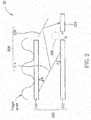
- FIG. 2 is a schematic diagram of another fingerprint capturing device 20 according to an embodiment of the present invention.
- the fingerprint capturing device 20 is derived from the fingerprint capturing device 10 of FIG. 1 , and the fingerprint capturing device 20 includes a capacitor sensing module 202, an image sensing module 204, a lighting component 206 and a reflective module 208, wherein the capacitor sensing module 202 includes a capturing platform 210 and a sensing electrode 212.
- the capturing platform 210 is utilized for receiving a finger press.
- the sensing electrode 212 generates a reference signal S when a capacitance variation is satisfied according to the finger press, which may be, for example, Flexible Print Circuit (FPC), Printed Circuit Board (PCB) or other non-transparent conductive film and so on.
- FPC Flexible Print Circuit
- PCB Printed Circuit Board
- the difference between the fingerprint capturing device 20 and the fingerprint capturing device 10 is that the reflective module 208 consists of the reflective mirrors 214 and 216, and in this example, the reflective mirror 214 respectively exists an angle A smaller than 90 with the capturing platform 210 and the sensing electrode 212, and position where the reflective mirror 216 locates is approximately parallel to the reflective mirror 214. However, positions, where the reflective mirrors 214 and 216 locate, change with position of the image sensing module 204, but not limited herein.
- the reference signal S is generated.
- the image sensing module 204 activates the light beam of the lighting component 206 to be reflected by the reflective mirror 214 and the reflective mirror 216, so as to generate the fingerprint ridges and fingerprint valleys of the fingerprint image on the image sensing module 204.
- the fingerprint capturing device 20 does not need to reflect the image of the fingerprint by the prism on the image sensing module 204, which can substantially reduce the volume of the device and be applied to mobile handy devices.
- the lighting component does not need to keep glowing all the time or intermittently emit lights, which saves the power consumption of the fingerprint capturing device and improves usage conveniences of the user.
- the embodiments stated in the above are utilized for illustrating the concept of the present invention.
- Those skilled in the art may make modifications and alterations accordingly, and not limited herein.
- the positions and ways for placing the reflective mirrors may be varied according to different usage scenarios, and the capacitance variation of the sensing electrode caused by the finger press to generate the reference signal can be changed according to statistics of experimental data, computational random or artificial settings, which are not limited herein, and all belong to the scope of the present invention.
- the present invention provides a capacitor/optic hybrid fingerprint detection device, such that the fingerprint capturing device does not need to keep the lighting component glowing all the time or intermittently emitting lights, and only needs to keep the lighting component on when necessary to capture the fingerprint, to achieve the advantages of low power consumption and improve comfort of the users.
Landscapes
- Engineering & Computer Science (AREA)
- Physics & Mathematics (AREA)
- Human Computer Interaction (AREA)
- General Physics & Mathematics (AREA)
- Multimedia (AREA)
- Theoretical Computer Science (AREA)
- Optics & Photonics (AREA)
- Image Input (AREA)
- Measurement Of The Respiration, Hearing Ability, Form, And Blood Characteristics Of Living Organisms (AREA)
Abstract
Description
- The present application is a continuation of international application No.
PCT/CN2016/101420, filed on October 1, 2016 - The present invention relates to a fingerprint capturing device, and more particularly, to a fingerprint capturing device of capacitor/optic hybrid.
- With the development of technology, mobile phones, digital cameras, tablet PCs, notebook computers and other portable electronic devices have become essential equipments for human life. To effectively avoid internal data of the personal portable electronic devices being stolen, all kinds of protection methods are provided. For example, password verification, voiceprint recognition or fingerprint recognition and so on, wherein optic fingerprint recognition is widely used. However, since a light source of a current optic fingerprint sensor has to stay on, in order to generate fingerprint images on an image sensing module, high power consumption occurs for long-time use. In addition, continuously or intermittently lighting of the light source affects sensation of users.
- It is therefore a primary objective of the present invention to provide a fingerprint capturing device of capacitor/optic hybrid and low power consumption.
- To solve the above mentioned technical problems, the present invention provides a fingerprint capturing device characterized by comprising a capacitor sensing module, for receiving a finger press to generate a reference signal according to the finger press, wherein the capacitor sensing module comprises a capturing platform and a sensing electrode; an image sensing module, connected to the capacitor sensing module, for activating a lighting component to emit a light beam after the capacitor sensing module generates the reference signal, so as to generate a fingerprint image of the finger.
- Preferably, the reference signal is generated when the sensing electrode receives the finger press and generates a capacitance variation.
- Preferably, the fingerprint capturing device further comprises a reflective module, for directing the light beam from the lighting component to the image sensing module, to generate the fingerprint image.
- Preferably, the reflective module comprises a prism and a condenser component.
- Preferably, the reflective module comprises a plurality of reflective mirrors.
- Preferably, when the reflective module consists of the prism and the condenser component, the light beam passes through the prism and is reflected by the condenser component to generate the fingerprint image on the image sensing module.
- Preferably, when the reflective module consists of the plurality of reflective mirrors, a first reflective mirror of the plurality of reflective mirrors respectively exists an angle smaller than 90 degrees with the capturing platform and the sensing electrode, such that the light beam passes through the first reflective mirror and a second reflective mirror of the plurality of reflective mirrors to generate the fingerprint image on the image sensing module.
- Preferably, the capturing platform is a glass.
- Preferably, the sensing electrode is one of a transparent conductive film, a double-sided flexible printed circuit board, or a printed circuit board.
- These and other objectives of the present invention will no doubt become obvious to those of ordinary skill in the art after reading the following detailed description of the preferred embodiment that is illustrated in the various figures and drawings.
-
-
FIG. 1 is a schematic diagram of a fingerprint capturing device according to an embodiment of the present invention. -
FIG. 2 is a schematic diagram of another fingerprint capturing device according to an embodiment of the present invention. - In order to make the objects, technical solutions and advantages of the present invention become more apparent, the following relies on the accompanying drawings and embodiments to describe the present invention in further detail. It should be understood that the specific embodiments described herein are only for explaining the present invention and are not intended to limit the present invention.
- Please refer to
FIG. 1. FIG. 1 is a schematic diagram of a fingerprint capturingdevice 10 according to an embodiment of the present invention. The fingerprint capturingdevice 10 includes acapacitor sensing module 102, animage sensing module 104, alighting component 106 and areflective module 108. Thecapacitor sensing module 102 is utilized for capturing a fingerprint and generating a reference signal S, which includes a capturingplatform 110 and a sensing electrode 112. The capturingplatform 110 is a place to receive a finger press, the sensing electrode 112 generates the reference signal S when a capacitance variation is satisfied according to the finger press; for example, when an user's finger presses the capturing platform 110 (e.g. a glass surface or an acrylic sheet), the sensing electrode 112, e.g. Indium Tin Oxide (ITO) or other transparent conductive film and so on, generates the reference signal S, when a capacitance variation is satisfied according to the finger press. Theimage sensing module 104 connects to the sensing electrode 112 of thecapacitor sensing module 102. After theimage sensing module 104 receives the reference signal S from the sensing electrode 112, theimage sensing module 104 activates thelighting component 106 to emit a light beam and generates fingerprint image of the finger. And thereflective module 108 directs the light beam from thelighting component 106 to theimage sensing module 104, such that the fingerprint image is generated on theimage sensing module 104 . Therefore, the fingerprint capturing device of the present invention does not need to activate the lighting component all the time, while utilizing the capacitor sensing module to activate the lighting component, to effectively reduce power consumption and provide more comfortable scenarios for the user. - In detail, in an embodiment, the
reflective module 108 of the fingerprint capturingdevice 10 includes aprism 114 and acondenser component 116, wherein theprism 114 is utilized for passing the light beam from thelighting component 106, and reflecting finger ridges and finger valleys of the finger, which presses on the capturingplatform 110, and by thecondenser component 116, e.g. a convex lens, the fingerprint image is generated on theimage sensing module 104. More specifically, when the finger presses on the capturing platform 110 (e.g. the glass surface or the acrylic sheet), such that the sensing electrode 112 (e.g. the transparent conductive film) satisfies the capacitance variation, the sensing electrode 112 generates the reference signal S. Then, when theimage sensing module 104 receives the reference signal S, which satisfies the capacitance variation, theimage sensing module 104 activates the light beam of thelighting component 106 to pass through theprism 114 and thecondenser component 116 to reflect and focus, such that theimage sensing module 104 generates the fingerprint image. Therefore, by the finger pressing the capacitor sensing module to activate the lighting component, the lighting component does not need to keep glowing all the time or intermittently emit lights, which saves the power consumption of the fingerprint capturing device and improves usage conveniences of the user. - In another embodiment, please refer to
FIG. 2. FIG. 2 is a schematic diagram of another fingerprint capturingdevice 20 according to an embodiment of the present invention. The fingerprint capturingdevice 20 is derived from the fingerprint capturingdevice 10 ofFIG. 1 , and thefingerprint capturing device 20 includes acapacitor sensing module 202, animage sensing module 204, alighting component 206 and areflective module 208, wherein thecapacitor sensing module 202 includes acapturing platform 210 and asensing electrode 212. The capturingplatform 210 is utilized for receiving a finger press. Thesensing electrode 212 generates a reference signal S when a capacitance variation is satisfied according to the finger press, which may be, for example, Flexible Print Circuit (FPC), Printed Circuit Board (PCB) or other non-transparent conductive film and so on. The difference between the fingerprint capturingdevice 20 and the fingerprint capturingdevice 10 is that thereflective module 208 consists of thereflective mirrors reflective mirror 214 respectively exists an angle A smaller than 90 with the capturingplatform 210 and thesensing electrode 212, and position where thereflective mirror 216 locates is approximately parallel to thereflective mirror 214. However, positions, where thereflective mirrors image sensing module 204, but not limited herein. That is, as long as the image of the fingerprint is generated on theimage sensing module 20 after being reflected by thereflective mirrors image sensing module 204 receives the reference signal S, which satisfies the capacitance variation, theimage sensing module 204 activates the light beam of thelighting component 206 to be reflected by thereflective mirror 214 and thereflective mirror 216, so as to generate the fingerprint ridges and fingerprint valleys of the fingerprint image on theimage sensing module 204. In addition, compared to the fingerprint capturingdevice 10, the fingerprint capturingdevice 20 does not need to reflect the image of the fingerprint by the prism on theimage sensing module 204, which can substantially reduce the volume of the device and be applied to mobile handy devices. Therefore, using the capacitance variation of the sensing electrode caused by the finger press to activate the lighting component, the lighting component does not need to keep glowing all the time or intermittently emit lights, which saves the power consumption of the fingerprint capturing device and improves usage conveniences of the user. - Notably, the embodiments stated in the above are utilized for illustrating the concept of the present invention. Those skilled in the art may make modifications and alterations accordingly, and not limited herein. For example, the positions and ways for placing the reflective mirrors may be varied according to different usage scenarios, and the capacitance variation of the sensing electrode caused by the finger press to generate the reference signal can be changed according to statistics of experimental data, computational random or artificial settings, which are not limited herein, and all belong to the scope of the present invention.
- In summary, the present invention provides a capacitor/optic hybrid fingerprint detection device, such that the fingerprint capturing device does not need to keep the lighting component glowing all the time or intermittently emitting lights, and only needs to keep the lighting component on when necessary to capture the fingerprint, to achieve the advantages of low power consumption and improve comfort of the users.
- Those skilled in the art will readily observe that numerous modifications and alterations of the device and method may be made while retaining the teachings of the invention. Accordingly, the above disclosure should be construed as limited only by the metes and bounds of the appended claims.
Claims (9)
- A fingerprint capturing device, characterized by comprising:a capacitor sensing module, comprising:a capturing platform, for receiving a finger press; anda sensing electrode, for generating a reference signal according to the finger press; andan image sensing module, connected to the sensing electrode, for activating a lighting component to emit a light beam after the sensing electrode generates the reference signal, so as to generate a fingerprint image of the finger.
- The fingerprint capturing device of claim 1, characterized in that, the reference signal is generated when the sensing electrode receives the finger press and generates a capacitance variation.
- The fingerprint capturing device of claims 1 or 2, characterized by further comprising:
a reflective module, for directing the light beam from the lighting component to the image sensing module, to generate the fingerprint image. - The fingerprint capturing device of claim 3, characterized in that, the reflective module comprises a prism and a condenser component.
- The fingerprint capturing device of claim 3, characterized in that, the reflective module comprises a plurality of reflective mirrors.
- The fingerprint capturing device of claim 4, characterized in that, when the reflective module consists of the prism and the condenser component, the light beam passes through the prism and is reflected by the condenser component to generate the fingerprint image on the image sensing module.
- The fingerprint capturing device of claim 5, characterized in that, when the reflective module consists of the plurality of reflective mirrors, a first reflective mirror of the plurality of reflective mirrors respectively exists an angle smaller than 90 degrees with the capturing platform and the sensing electrode, such that the light beam passes through the first reflective mirror and a second reflective mirror of the plurality of reflective mirrors to generate the fingerprint image on the image sensing module.
- The fingerprint capturing device of any of claims 1-7, characterized in that, the capturing platform is a glass.
- The fingerprint capturing device of any of claims 1-7, characterized in that, the sensing electrode is one of a transparent conductive film, a double-sided flexible printed circuit board, or a printed circuit board.
Applications Claiming Priority (1)
| Application Number | Priority Date | Filing Date | Title |
|---|---|---|---|
| PCT/CN2016/101420 WO2018058694A1 (en) | 2016-10-01 | 2016-10-01 | Fingerprint capture device |
Publications (2)
| Publication Number | Publication Date |
|---|---|
| EP3333760A1 true EP3333760A1 (en) | 2018-06-13 |
| EP3333760A4 EP3333760A4 (en) | 2018-09-05 |
Family
ID=58215988
Family Applications (1)
| Application Number | Title | Priority Date | Filing Date |
|---|---|---|---|
| EP16898151.2A Withdrawn EP3333760A4 (en) | 2016-10-01 | 2016-10-01 | Fingerprint capture device |
Country Status (5)
| Country | Link |
|---|---|
| US (1) | US10621403B2 (en) |
| EP (1) | EP3333760A4 (en) |
| KR (1) | KR20180050600A (en) |
| CN (1) | CN106462759A (en) |
| WO (1) | WO2018058694A1 (en) |
Families Citing this family (4)
| Publication number | Priority date | Publication date | Assignee | Title |
|---|---|---|---|---|
| CN106960194A (en) * | 2017-03-24 | 2017-07-18 | 徐晨 | A kind of vein identification device |
| JPWO2019107459A1 (en) * | 2017-11-29 | 2020-12-10 | 日本板硝子株式会社 | Decorative material |
| CN109074492B (en) | 2018-08-06 | 2022-08-26 | 深圳市汇顶科技股份有限公司 | Optical fingerprint identification device under screen and electronic equipment |
| CN111126305A (en) * | 2019-03-25 | 2020-05-08 | 神盾股份有限公司 | Fingerprint Sensing Device |
Family Cites Families (17)
| Publication number | Priority date | Publication date | Assignee | Title |
|---|---|---|---|---|
| US5629764A (en) * | 1995-07-07 | 1997-05-13 | Advanced Precision Technology, Inc. | Prism fingerprint sensor using a holographic optical element |
| US5650842A (en) * | 1995-10-27 | 1997-07-22 | Identix Incorporated | Device and method for obtaining a plain image of multiple fingerprints |
| GB9725571D0 (en) * | 1997-12-04 | 1998-02-04 | Philips Electronics Nv | Electronic apparatus comprising fingerprint sensing devices |
| US6582088B2 (en) * | 2000-08-10 | 2003-06-24 | Benq Corporation | Optical path folding apparatus |
| US6980286B1 (en) * | 2001-10-25 | 2005-12-27 | Ic Media Corporation | Ultra-thin optical fingerprint sensor with anamorphic optics |
| US6750955B1 (en) * | 2002-03-14 | 2004-06-15 | Ic Media Corporation | Compact optical fingerprint sensor and method |
| JP4658443B2 (en) * | 2002-12-19 | 2011-03-23 | カシオ計算機株式会社 | Image input device |
| JP2007167471A (en) * | 2005-12-26 | 2007-07-05 | Sharp Corp | Biological information processing apparatus and biological information processing method |
| CN101046845A (en) * | 2006-03-28 | 2007-10-03 | 敦南科技股份有限公司 | Optical fingerprint capture device with finger contact detection function and method thereof |
| US20080239285A1 (en) * | 2007-03-30 | 2008-10-02 | Chuan Liang Industrial Co., Ltd. | Fingerprint identification system |
| KR100967655B1 (en) | 2008-06-03 | 2010-07-07 | 씨큐트로닉스 (주) | Optical fingerprint input device and fingerprint recognition method using same |
| CN201465142U (en) * | 2009-06-11 | 2010-05-12 | 成都方程式电子有限公司 | Induction type optical fingerprint collecting device |
| CN102750520A (en) * | 2012-06-05 | 2012-10-24 | 东莞市中控电子技术有限公司 | Capacitive fingerprint detection device |
| CN202677425U (en) * | 2012-07-12 | 2013-01-16 | 邓国强 | Capacitive type sensing device and optical fingerprint gatherer |
| US9002586B2 (en) * | 2012-12-03 | 2015-04-07 | Honda Motor Co., Ltd. | Integrated biometric switch |
| RU2597465C2 (en) * | 2015-01-23 | 2016-09-10 | Антон Сергеевич Прытков | Compact papillary picture recording system |
| US10102411B2 (en) * | 2017-01-25 | 2018-10-16 | Synaptics Incorporated | Hybrid optical and capacitive sensor |
-
2016
- 2016-10-01 EP EP16898151.2A patent/EP3333760A4/en not_active Withdrawn
- 2016-10-01 KR KR1020177031884A patent/KR20180050600A/en not_active Ceased
- 2016-10-01 CN CN201680001056.6A patent/CN106462759A/en active Pending
- 2016-10-01 WO PCT/CN2016/101420 patent/WO2018058694A1/en not_active Ceased
-
2017
- 2017-10-16 US US15/784,201 patent/US10621403B2/en active Active
Also Published As
| Publication number | Publication date |
|---|---|
| WO2018058694A1 (en) | 2018-04-05 |
| EP3333760A4 (en) | 2018-09-05 |
| US10621403B2 (en) | 2020-04-14 |
| CN106462759A (en) | 2017-02-22 |
| KR20180050600A (en) | 2018-05-15 |
| US20180096184A1 (en) | 2018-04-05 |
Similar Documents
| Publication | Publication Date | Title |
|---|---|---|
| US11294152B2 (en) | Optical device for fingerprint collection | |
| US10621403B2 (en) | Fingerprint capturing device | |
| US9134866B2 (en) | Dry/wet touch screen | |
| TWI470507B (en) | Interactive surface computer with switchable diffuser | |
| EP3644222A1 (en) | Backlight module, below-screen fingerprint recognition method and apparatus, and electronic device | |
| CN109284742A (en) | Under-screen fingerprint module, electronic device and fingerprint image processing method | |
| WO2020077505A1 (en) | Under-display fingerprint recognition apparatus and electronic device | |
| CN106973212B (en) | Camera device and mobile terminal | |
| CN103988142B (en) | portable device | |
| WO2018137165A1 (en) | Electronic device | |
| KR20150032028A (en) | Three dimensional space-touch screen apparatus and method using the same | |
| KR20190013339A (en) | Electronic device and method for controlling thereof | |
| US8350828B2 (en) | Touch screen apparatus with reflector | |
| US20180130442A1 (en) | Anti-spy electric device and adjustable focus glasses and anti-spy method for electric device | |
| CN110244848B (en) | Reading control method and related equipment | |
| CN110381188A (en) | Mobile terminal and its application method | |
| CN106990859B (en) | Optical touch system, optical touch device and touch detection method thereof | |
| WO2021238553A1 (en) | Under-screen recognition assembly and electronic device | |
| CN101576787B (en) | Electric equipment, notebook computer and method for realizing touch control | |
| CN111339815A (en) | An optical detection device and electronic equipment | |
| WO2020056547A1 (en) | Biometric imaging device | |
| CN101685350B (en) | Computer input device, bispectral data input processing method and sensor thereof | |
| US20200151483A1 (en) | Optical device for fingerprint collection | |
| CN108762487A (en) | electronic device | |
| CN114267055A (en) | Optical fingerprint module and electronic equipment |
Legal Events
| Date | Code | Title | Description |
|---|---|---|---|
| STAA | Information on the status of an ep patent application or granted ep patent |
Free format text: STATUS: UNKNOWN |
|
| STAA | Information on the status of an ep patent application or granted ep patent |
Free format text: STATUS: THE INTERNATIONAL PUBLICATION HAS BEEN MADE |
|
| PUAI | Public reference made under article 153(3) epc to a published international application that has entered the european phase |
Free format text: ORIGINAL CODE: 0009012 |
|
| STAA | Information on the status of an ep patent application or granted ep patent |
Free format text: STATUS: REQUEST FOR EXAMINATION WAS MADE |
|
| 17P | Request for examination filed |
Effective date: 20171018 |
|
| AK | Designated contracting states |
Kind code of ref document: A1 Designated state(s): AL AT BE BG CH CY CZ DE DK EE ES FI FR GB GR HR HU IE IS IT LI LT LU LV MC MK MT NL NO PL PT RO RS SE SI SK SM TR |
|
| AX | Request for extension of the european patent |
Extension state: BA ME |
|
| RIC1 | Information provided on ipc code assigned before grant |
Ipc: G06K 9/00 20060101AFI20180713BHEP |
|
| A4 | Supplementary search report drawn up and despatched |
Effective date: 20180806 |
|
| DAV | Request for validation of the european patent (deleted) | ||
| DAX | Request for extension of the european patent (deleted) | ||
| STAA | Information on the status of an ep patent application or granted ep patent |
Free format text: STATUS: EXAMINATION IS IN PROGRESS |
|
| 17Q | First examination report despatched |
Effective date: 20200415 |
|
| STAA | Information on the status of an ep patent application or granted ep patent |
Free format text: STATUS: THE APPLICATION IS DEEMED TO BE WITHDRAWN |
|
| 18D | Application deemed to be withdrawn |
Effective date: 20230503 |