EP3333600A1 - Tunable optical devices and their methods of manufacturing - Google Patents
Tunable optical devices and their methods of manufacturing Download PDFInfo
- Publication number
- EP3333600A1 EP3333600A1 EP16202392.3A EP16202392A EP3333600A1 EP 3333600 A1 EP3333600 A1 EP 3333600A1 EP 16202392 A EP16202392 A EP 16202392A EP 3333600 A1 EP3333600 A1 EP 3333600A1
- Authority
- EP
- European Patent Office
- Prior art keywords
- layer
- holes
- filter
- optical device
- optical
- Prior art date
- Legal status (The legal status is an assumption and is not a legal conclusion. Google has not performed a legal analysis and makes no representation as to the accuracy of the status listed.)
- Withdrawn
Links
Images


Classifications
-
- G—PHYSICS
- G02—OPTICS
- G02B—OPTICAL ELEMENTS, SYSTEMS OR APPARATUS
- G02B5/00—Optical elements other than lenses
- G02B5/008—Surface plasmon devices
-
- G—PHYSICS
- G02—OPTICS
- G02B—OPTICAL ELEMENTS, SYSTEMS OR APPARATUS
- G02B5/00—Optical elements other than lenses
- G02B5/20—Filters
- G02B5/204—Filters in which spectral selection is performed by means of a conductive grid or array, e.g. frequency selective surfaces
-
- G—PHYSICS
- G02—OPTICS
- G02B—OPTICAL ELEMENTS, SYSTEMS OR APPARATUS
- G02B5/00—Optical elements other than lenses
- G02B5/20—Filters
- G02B5/28—Interference filters
- G02B5/281—Interference filters designed for the infrared light
-
- G—PHYSICS
- G02—OPTICS
- G02B—OPTICAL ELEMENTS, SYSTEMS OR APPARATUS
- G02B5/00—Optical elements other than lenses
- G02B5/20—Filters
- G02B5/28—Interference filters
- G02B5/284—Interference filters of etalon type comprising a resonant cavity other than a thin solid film, e.g. gas, air, solid plates
-
- G—PHYSICS
- G02—OPTICS
- G02B—OPTICAL ELEMENTS, SYSTEMS OR APPARATUS
- G02B5/00—Optical elements other than lenses
- G02B5/20—Filters
- G02B5/28—Interference filters
- G02B5/285—Interference filters comprising deposited thin solid films
- G02B5/288—Interference filters comprising deposited thin solid films comprising at least one thin film resonant cavity, e.g. in bandpass filters
Definitions
- the present invention relates to the field of optical devices. More particularly, the present invention relates to micro-machined narrow-band optical devices, in particular optical filters comprising an electrically conducting membrane comprising an array of apertures.
- Optical filters are important optical elements that are commonly used in a variety of optical systems and optical components.
- a great variety of optical systems and devices require the use and incorporation of narrow-band optical filters for applications such as chip scale spectrometers, color image sensors, hyperspectral image sensors, color flat panel displays.
- a well-known narrow-band filter is a multilayer dielectric filter comprising a stack of dielectric layers such as TiO 2 and SiO 2 layers.
- Multilayer dielectric filters are limited to the available materials that are transparent in the visible and infrared part of the electromagnetic spectrum. Also, making dielectric filter stacks can be difficult and expensive to make especially in the infrared as the filter stack thickness is proportional to the operating wavelength.
- the simplest narrowband optical filter that can be fabricated consist in two metal layers that are separated by a spacer. These filters, known as Fabry-Perot filters, are quite simple to fabricate and cheap. On the other hand they have two major drawbacks.
- the first drawback is that the maximum optical transmission is limited by the intrinsic absorption in the metal layers. In the visible spectrum, this limits the transmission and the linewidth of the transmitted optical beam by the filter.
- a narrow linewidth filter has a poor transmission and vice versa - a filter with good transmission has a broad linewidth.
- the optical characteristics of the filter cannot be changed once the filter is fabricated. More precisely, the central wavelength of the transmitted beam cannot be modified as it is fixed by the materials and geometry of the Fabry-Perot filter.
- Plasmonic filters are described for example in: E. Shaner et al., Plasmonic Filters, Sandia Report SAND2009-5990, sep. 2009 .
- a Fabry-Perot filter comprises two metal films, separated by a spacer, and in which at least one of the metal layers comprises a periodic subwavelength hole structure or a periodic array of metallic islands separated by subwavelength sized openings.
- the device in in PCT/US2007/026071 has an embedded plasmonic metal filter comprising an array of periodic subwavelength apertures.
- the plasmonic device array patterns are configured such that when light is incident on the array structures, at least one plasmon mode is resonant with the incident light to produce a transmission spectral window with the desired spectral profile, bandwidth and beam shape.
- the transmission spectral window functions as an embedded passband filter for the Fabry-Perot filter.
- the plasmonic filter in the device disclosed in PCT/US2007/026071 has a high reflectivity but has a high absorption loss. Also, because of the periodic structure of the array of holes the plasmonic device of PCT/US2007/026071 , diffraction effects are important and the device is also prone to scattering losses which limits the filter performance. The high absorption losses, the diffraction and scattering prohibit achieving a high intensity of the transmitted optical beam.
- the invention is also achieved by a method to fabricate the optical device and a method to fabricate the Fabry-Perot filter.
- an optical device comprising an electrically conductive membrane defining a plane and comprising a two dimensional array of through-holes, extending through a thickness of the electrically conductive membrane between opposite surfaces being parallel to said plane, the electrically conductive membrane being arranged to reflect and transmit at least a portion of an incident light beam on the optical filter.
- the through-holes form apertures in said opposite surface and have a circumference, defined in any cross section parallel to said plane, of less than the wavelength of said incident light beam.
- said electrically conducting membrane is made of a material having a dielectric constant comprising a real part and an imaginary part, said real part being smaller than -2 and an absolute value of the ratio of the imaginary part to the real part of the dielectric constant being less than 0.1.
- At least a dielectric layer is arranged to at least one side of said electrically conductive membrane.
- said dielectric layer comprises pores.
- said pores comprise at least a portion of through-holes extending from one side of the dielectric layer to an opposite side of the dielectric layer.
- said electrically conducting membrane is a metallic membrane.
- said electrically conducting membrane comprises at least two different arrays of holes.
- a tunable Fabry-Perot filter comprising an optical device as described before and which is arranged on a first surface of a gap layer and which further comprising a reflective layer arranged on a second surface of the gap layer opposite and parallel to said first surface.
- Said reflective layer comprises an array of through-holes.
- the reflective layer is a second electrical conducting membrane.
- the second electrical conducting membrane is a second optical filter as described above.
- the reflective layer is a stack of dielectric layers.
- the gap layer comprises pores.
- said pores are channels extending through a thickness of said gap layer between said first surface and the second surface thereof, said channels connecting the through holes of the first optical device and the reflecting layer.
- the gap layer is an air layer.
- the gap layer comprises at least a dielectric layer.
- the invention is also achieved by a method of fabrication of the optical filter and comprising the steps of:
- step e) comprises the etching through said dielectric layer, so as to form an array of through-holes of which through- holes extend from said front dielectric surface to said device layer back surface.
- the invention is also achieved by a method to tune the optical characteristics of the tunable Fabry-Perot filter as described before.
- This tuning method comprises the following steps:
- the etching is performed so as that that the central transmitted wavelength of a transmitted light beam by said Fabry-Perot filter is changed.
- the etching is performed so that the spectral width of a transmitted light beam by said Fabry-Perot filter is changed.
- Fig.1a and Fig.1b illustrate two preferred embodiments of the optical device 1.
- the optical device 1 of the invention comprises an electrically conductive membrane 10, also defined as first reflecting layer, having a front surface 14 and a back surface 16 and defining a plane in between said front and back surface 16, and comprises a two dimensional non-periodic array 13 of through-holes 12, extending through a thickness of the electrically conductive membrane 10 between said opposite surfaces 14, 16.
- the electrically conductive membrane 10 is arranged to reflect and transmit at least a portion of an incident light beam on the optical device 1. Therefore the optical device 1 is also defined as an optical reflector or a mirror that is semi-transparent.
- the optical device 1 may also be defined as an optical filter.
- the optical device 1 may be a single electrically conductive layer 10 as illustrated in Fig. 1a .
- the optical device 1 may comprise the electrically conductive layer 10 arranged to a holder or frame or support as illustrated in Fig. 1b .
- the electrically conductive layer 10 and its supporting frame may be realized, as explained further in the method of fabrication, in structured silicon on insulator wafer, hereafter defined as an SOI wafer.
- Said supporting frame may comprise several layers 1 a, 1 b, and 1 c such as shown in Fig. 1 a.
- Said through-holes 12 forming apertures 12a, 12b respectively in said opposite surfaces 14,16, and define a structural factor S(k), being the Fourier transform of the positional arrangement of the through-holes in the plane 11 of the electrically conducting membrane 10:
- the through holes have a circumference, defined in any cross section parallel to said plane, that is smaller than the wavelength of the incident light for which the optical device is designed.
- the through holes may have any shape. It is understood that preferably the holes 12 are perpendicular to said plane 11 and have preferably a cylindrical shape. But in variants the holes 12, each defining a hole axis 12a, may have a slight angle relative to the perpendicular axis to said plane 11.
- the holes may also have non-uniform cross sections, defined in any plane perpendicular to said hole axis 12a. In particular said aperture 12a may have a different size and shape as the aperture 12b.
- any object used in as part of a filter should have low loss in order to have a high potential transmissivity.
- loss is only due to absorption in the layer.
- the former lead to scattering and diffraction losses while the latter may excite surface plasmons (both localized and propagating).
- power is lost from the principle direction of the impinging light.
- the integral of the structural factor should be small, in this embodiment the other losses are less than 0.05 or preferably zero.
- said electrically conducting membrane 10 is made of a material having a dielectric constant at the wavelength of operation comprising a real part and an imaginary part, said real part being smaller than -2 and an absolute value of the ratio of the imaginary part to the real part of the dielectric constant being less than 0.1.
- a conducting membrane with these properties will have a bulk (unstructured, infinitely thick film) reflectivity of greater than 80%.
- the essence of the invention is related to the fact that the invented electrically conducting membrane 10 , comprising a array of holes 13 with subwavelength holes 12 that are distributed a-periodically, also defined as random, has a very low absorption compared to structures of prior art as described in PCT/US2007/026071 , which comprises a plasmonic filter having periodic holes.
- the loss is a generalized loss term and could be due to diffraction or scattering as well as material loss.
- the potential transmission of the system is just the product of the potential transmission of the individual layers or sets of layers.
- the utility of a layer is limited by the potential transmission. If one wants to make filters with high transmission then the potential transmission should be high. If we want to make for example Fabry-Perot filters with a narrow finesse, then the reflectivity of the layers on each side of the FP cavity should have high reflectivity. Thus the utility of a layer in such a filter depends on having both a high potential transmission and simultaneously a high reflectivity, R.
- Standard metal mirrors can either have high reflectivity and low potential transmissivity or vice versa. Despite the fact that metals in the infrared have higher reflectivity than in the visible, their potential transmissivity is considerably lower. Metal mirrors are not useful for making Fabry Perot filters in the infra-red. There are additional technical issues such as having very thin continuous metal layers which also make metal mirrors unfavourable for Fabry-Perot filters.
- Figure 8 shows the potential transmission of a silver layer on glass as a function of reflectivity at 650 nm.
- the graph shows the comparison between a conventional Fabry-Perot optical filter without holes and a Fabry-Perot optical filter 50 of the invention comprising a reflecting layer comprising an array of holes 13.
- the width of the spacer layer in the Fabry-Perot is half the wavelength.
- the ratio or area of the holes to the area of the metal area is a factor of 1/4.
- the linewidth of the FP and the transmission depend both on the thickness of the metal layer, which is varied parametrically in this graph.
- the graph shows the comparative transmissions for the case of a Fabry-Perot designed for visible and infrared central wavelengths, respectively 0.65 ⁇ m and 6.5 ⁇ m respectively. Note that, for example, for 50% transmission the linewidth at 6.5 ⁇ m improves by an order of magnitude when array of holes are used compared to the traditional FP filters without holes.
- the potential transmissivity can be increased by more than an order of magnitude while keeping the same reflectivity.
- the pores in the metal layer must be arranged so that they produce low loss, i.e. no or little scattering, no or little diffusion - any arrangement that has properties of so-called stealth hyper-uniformity are excellent candidates, there should also be little loss due to the coupling of surface plasmons, i.e., any periodicities n the structure should be at periods of at most half the operating wavelength. It should be noted that these arrangements leading to plasmonic filters while they have high potential transmission, they have low reflectivity.
- the holes in the porous metal layer should be small enough that there are no propagating modes within those holes - otherwise the light will pass through the porous metal layer relatively unhindered and high reflectivity cannot be achieved.
- the general condition for this is that the circumference of the holes is less than the wavelength of light.
- Another advantage of the invention is that it allows realizingoptical filter arrays that may be realized on a single membrane, each filter array may have a different optical characteristic.
- the optical device 1 comprises a plurality of arrays 13 comprising at least two different arrays of holes 13, each array of holes having different optical characteristics.
- the at least two different array of holes 13 may have different holes dimensions and/or different hole positions and/or cross shapes of the holes.
- a first section of the optical device 1 comprises a first array of holes 13a in the optical filter 1 may be arranged to transmit a visible light beam and a second section comprises a second array 13b that may be arranged to transmit near-infra-red light.
- a visible light beam having a wavelength ⁇ 1 may be transmitted by a first section comprising a first array 13a of through holes and a second light beam having a wavelength ⁇ 2 may be transmitted by a second section of the optical device comprising a second array 13b of through holes.
- a plurality of different array of holes 13 are arranged as a linear array.
- a plurality of different array of holes 13 are arranged in the optical device 1 as a two dimensional array, for example a rectangular or circular shaped array.
- the plurality of array of holes may be adjacent array of holes or may be separated by areas of the optical device 1 that do not comprise holes.
- optical device1 of the invention concern UV, visible or infrared light but the optical device1 might be used for far-UV and X-ray applications
- a dielectric layer 150 may be arranged to at least one side of said electrically conductive membrane 10.
- This dielectric layer 150 may be a continuous layer or may comprise through-holes aligned with the through-holes 12 of the electrically conducting membrane 10.
- said dielectric layer 150 may be a porous layer, i.e. comprising pores. Said pores may be voids or apertures extending from one side of said dielectric layer 150. The pores may also be random shaped and distributed channels in said dielectric layer.
- one may deposit a metallic or dielectric reflecting layer on said dielectric layer 150 to form a tunable Fabry-Perot filter 50.
- the pores in the dielectric layer improve the etching efficiency of the dielectric layer 150 in such a tunable Fabry-Perot filter.
- the cross-section of the pores in the dielectric layer in a plane parallel to the surface should be less than twice the operating wavelength.
- the electrically conducting layer may be a composite layer comprising layers made of different conducting materials, such as the combination of a metallic layer and a conducting polymer
- the invention is also achieved by a tunable Fabry-Perot filter 50, also defined as Fabry-Perot filter 50, which comprises at least one optical device 1 as described above.
- Said tunable Fabry-Perot filter 50 shown in Fig. 2a comprises a gap layer 40 defining a first surface 44 and a second surface 46 parallel and opposite to said first surface 44.
- the tunable Fabry-Perot filter 50 comprises at least a second reflecting layer 20, also defined as reflecting membrane, arranged to said second surface 46.
- Said second reflecting layer 20 may be an electrically conducting layer, preferably a metal layer.
- the second reflecting layer may be a stack of dielectric layers.
- a metallic layer may be arranged to at least one of the sides of said stack.
- the gap layer 40 is preferably a dielectric layer or may be a layer of air.
- the gap layer 40 may be a stack of dielectric layers.
- the gap layer may also be made of amorphous or crystalline and/or doped silicon.
- the gap 40 may comprise at least two layers made in a material chosen from: a metal, a dielectric or a semiconductor material.
- said gap layer 40 and said second reflecting layer 20 have no through holes.
- said gap layer 40 is a porous gap layer, comprising pores as defined above in an embodiment of the optical device 1.
- the gap layer 40 is porous it may comprise pores, voids and through holes.
- the gap layer 40 only comprises through holes which may not be aligned with the through holes 12 of the optical device 1.
- said gap layer 40 has through-holes 42 extending from said first surface 44 to said second surface 46 and the through holes 42 are aligned with the through-holes 12 of said electrically conducting layer 10 but may be slightly misaligned by some nm.
- said reflecting layer 20 comprises an array of through-holes 22 that may be slightly misaligned with the through holes 12 of said first electrically conducting layer 10 and/or the through holes 42 of the gap layer 40.
- the through-holes 22 in said reflecting layer20 are distributed a-periodically, but may be distributed periodically.
- the through-holes 22 in said reflecting layer 20 comprise a portion of holes 22 that have a periodic distribution.
- the tunable Fabry-Perot filter 50 comprises a porous dielectric gap layer 40 and a dielectric reflecting stack 20 as illustrated in Fig.2b .
- the reflecting layer 20 is a second electrical conducting membrane.
- the reflecting layer 20 is a second optical filter 1' that is identical to said first optical filter 1.
- the dielectric gap layer 40 is a gap layer made in SiO 2 comprising gap channels 42 extending through the thickness of the gap 40, said channels 42 extending between said first surface 44 and said second surface 46 thereof. Said channels 42 connect the through-holes 12, 22 of respectively the first 10 and the reflecting layer 20. Even in the case that said second reflecting layer 20 is identical to the first electrically conducting membrane 10 is identical the second reflecting layer 20 may have a slight offset relative to the electrically conducting membrane 10. This offset may of some nm defined in a plane parallel to said plane 11 of the first electrical conducting membrane 10.
- the gap layer 40 is made of silicon (Si).This may be amorphous silicon or crystalline silicon.
- the silicon layer may be a doped silicon layer.
- the gap layer 40 is an air layer.
- the advantage of having an air layer 40 in the tunable Fabry-Perot filter 50 is that at least one of said first electrically conducting membrane and said reflecting layer may be displaced in the direction perpendicular to said plane 11.
- an actuator may be adapted to the tunable Fabry-Perot filter 50. Actuators to move a membrane perpendicular to its plane are well known to the skilled person and will not be further described here.
- the method to fabricate a Fabry-Perot filter 50 comprising an air layer 40 is further described in the paragraphs of this document related to the method of fabrication.
- the inventors have discovered that the alignment between the holes 12, 22 in the layers 110,120,130, 140 of the tunable Fabry-Perot filter 50 is not crucial for functioning of the filter if the critical dimension of the holes is much smaller than the operating wavelength and if the periodocity of the through holes 12 is smaller than the wavelength in both the surrounding medium, which is preferably air, and the material of the gap layer 40.
- the filter 50 may be tuned by a postprocessing process as described further.
- the postprocessing is performed by etching the gap layer 40 through the through-holes.
- the uniform postprocess etching of the gap layer 40 allows to tune the optical characteristics of the Fabry-Perot filter 50.
- the tuning may consist of changing the central wavelength and/or the bandwidth of the Fabry-Perot filter 50.
- the tunable Fabry-Perot filter 50 comprises portions that have different sections of the gap layer 40 that have different thickness, defined perpendicular to said plane 11. This may be achieved by etching away a portion of the gap layer 40 as further described. By etching away a portion of the gap layer the central wavelength and/or spectral width of the transmitted light by the Fabry-Perot filer may be tuned. This postprocessing of a tunable Fabry-Perot filter 50 allows realizing a tunable Fabry-Perot filter 50 that comprises an array of tunable Fabry-Perot filters realized in a single filter.
- the postprocessing may be made more efficient by using a porous dielectric gap layer 40, as the etching gases or chemicals may penetrate more easily in the gap layer 40 and as such enhancing the removal of material of the gap layer and as such changing considerably the local volume and refractive index of the gap layer.
- the invention is further achieved by method of fabrication of the optical device1, illustrated in Figs.3a-c comprising the steps of:
- step e) comprises the etching through said dielectric layer 150, so as to form an array of through-holes13 of which through- holes 12 extend from said front dielectric surface 152 to said device layer back surface 134.
- the invention is also achieved by a method of fabrication of method a tunable Fabry-Perot filter 50 as described above. This method comprises the main steps of:
- Said spacing layer 240 may have different geometries such as an array of cantilevers or may be a shoulder structure as further described.
- steps a)-d) are illustrated in Fig.3a
- step f) is illustrated in Fig.3a
- step g) is illustrated in Fig.3a .
- step c) is realized by (Fig.4a):
- the two optical filters 1,1' are fixed to the spacing structure 202, i.e. the structured second SOI wafer 200, by a gluing technique as illustrated in Fig 4b : different variants of the fixing or attachment technique the two optical devices 1, 1' to the spacing structure 202 may be used such as welding or bonding techniques and the fixing may be performed between different parts of the tow optical device 1, 1' to the spacing structure 202.
- the alternatives of the fixing techniques well known and will not be further described here.
- said shoulder 200c may have different shapes, such as a plurality of beams, or a ring shaped shoulder. It is also understood that said shoulder 200c and/or the first or second optical device 1,1' may comprise at least one adhesion layers allowing to fix at least one of said optical device 1,1' to said shoulder structure 200c. It is understood that this adhesion layer may be any adhesion layer such as a layer allowing to solder or to realize an attachment by any kind of fusion technique, including fusion by laser or heating techniques
- the invention is also achieved by a method to fabricate a tunable Fabry-Perot filter 50 of the invention and uses thermocompresion techniques, illustrated in Figs 6a, 6b and comprises the steps of:
- a Fabry-Perot filter 50 comprising a dielectric layer 40 between two electrically conduction layers is realized according to process steps illustrated in Fig.7 .
- the main process steps are the following.
- Fig.7a illustrates the steps of:
- Fig. 7b illustrates the steps of:
- Fig. 7c illustrates the steps of:
- Fig. 7d illustrates the steps of etching the buried oxide layer 120
- any remaining oxide layer may be removed, such as the device layer portions 130 as illustrated in Fig.7d .
- the invention is also achieved by a method to tune the optical characteristics of the tunable Fabry-Perot filter 50 as described before.
- This tuning method comprises the following steps:
- the etching is performed so as that that the central transmitted wavelength of a transmitted light beam by said Fabry-Perot filter 50 is changed.
- Fabry-Perot filters of the invention have been realized and characterised.
- a Fabry-Perot filter designed for infrared applications between 9-18 ⁇ m has the following technical features:
- the diameters of the holes 12 are 2 ⁇ m and arranged in a hexagonal lattice with a period of 3.6 ⁇ m.
- the measured Fabry-Perot 50 has a central silicon spacer of 5 ⁇ m.
- a 50nm thick Au layer is deposited on both sides 44, 46 of the silicon layer 40.
- the holes 12 extend through the entire sandwich structure, i.e. the stack of layers Au-Si-Au.
- This Fabry-Perot filter 50 was measured in transmission using a liquid nitrogen cooled Mercury Cadmium Telluride detector in a Fourier transform infrared spectrometer microscope (Bruker-Hyperion).
- Figure 9 shows the transmission measurements.
- the two Fabry-Perot peaks have approximately 10% transmission and a 1.5% linewidth. It can be calculated from the free spectral range and the linewidth of the given filter that the finesse is around 43.5. Consequently, the effective reflectivity of the porous mirrors is around 93%.
- a conventional metal / silicon / metal Fabry-Perot having the same geometrical configuration but without comprising an array of holes, having a similar linewidth, would have a transmission of only 0.2%.
- the Fabry-Perot filter of the invention has a transmission that is 50 times higher than a conventional Fabry-Perot filter.
Landscapes
- Physics & Mathematics (AREA)
- General Physics & Mathematics (AREA)
- Optics & Photonics (AREA)
- Spectroscopy & Molecular Physics (AREA)
- Mechanical Light Control Or Optical Switches (AREA)
- Optical Filters (AREA)
Abstract

Description
- The present invention relates to the field of optical devices. More particularly, the present invention relates to micro-machined narrow-band optical devices, in particular optical filters comprising an electrically conducting membrane comprising an array of apertures.
- Optical filters are important optical elements that are commonly used in a variety of optical systems and optical components. In particular, a great variety of optical systems and devices require the use and incorporation of narrow-band optical filters for applications such as chip scale spectrometers, color image sensors, hyperspectral image sensors, color flat panel displays.
- A well-known narrow-band filter is a multilayer dielectric filter comprising a stack of dielectric layers such as TiO2 and SiO2 layers. Multilayer dielectric filters are limited to the available materials that are transparent in the visible and infrared part of the electromagnetic spectrum. Also, making dielectric filter stacks can be difficult and expensive to make especially in the infrared as the filter stack thickness is proportional to the operating wavelength.
- The simplest narrowband optical filter that can be fabricated consist in two metal layers that are separated by a spacer. These filters, known as Fabry-Perot filters, are quite simple to fabricate and cheap. On the other hand they have two major drawbacks. The first drawback is that the maximum optical transmission is limited by the intrinsic absorption in the metal layers. In the visible spectrum, this limits the transmission and the linewidth of the transmitted optical beam by the filter. A narrow linewidth filter has a poor transmission and vice versa - a filter with good transmission has a broad linewidth. Secondly, the optical characteristics of the filter cannot be changed once the filter is fabricated. More precisely, the central wavelength of the transmitted beam cannot be modified as it is fixed by the materials and geometry of the Fabry-Perot filter. Furthermore it would be extremely difficult to realize a matrix of Fabry-Perot filters having each different central transmitted wavelength, as the thickness of the spacer layer would have to be different across the wafer on which the filter layers are deposited. Taking into account that making Fabry-Perot filter requires a stringent control of the thicknesses and the fact that the process requires multiple processing steps, making matrices would be a difficult task.
- In order to avoid the use that stack of dielectric layers and also to cope with the limitations of Fabry-Perot filter based on continuous metal layers some developments have been made based on plasmonic filters. Plasmonic filters are described for example in: E. Shaner et al., Plasmonic Filters, Sandia Report SAND2009-5990, sep. 2009.
- In a realization disclosed in
PCT/US2007/026071 , a Fabry-Perot filter is proposed that comprises two metal films, separated by a spacer, and in which at least one of the metal layers comprises a periodic subwavelength hole structure or a periodic array of metallic islands separated by subwavelength sized openings. The device in inPCT/US2007/026071 has an embedded plasmonic metal filter comprising an array of periodic subwavelength apertures. The plasmonic device array patterns are configured such that when light is incident on the array structures, at least one plasmon mode is resonant with the incident light to produce a transmission spectral window with the desired spectral profile, bandwidth and beam shape. The transmission spectral window functions as an embedded passband filter for the Fabry-Perot filter. - The plasmonic filter in the device disclosed in
PCT/US2007/026071 has a high reflectivity but has a high absorption loss. Also, because of the periodic structure of the array of holes the plasmonic device ofPCT/US2007/026071 , diffraction effects are important and the device is also prone to scattering losses which limits the filter performance. The high absorption losses, the diffraction and scattering prohibit achieving a high intensity of the transmitted optical beam. - It is the aim of this invention to provide an optical device and a Fabry-Perot filter having improved optical performances relative to the filters and Fabry-Perot filters of prior art.
- The invention is also achieved by a method to fabricate the optical device and a method to fabricate the Fabry-Perot filter.
- More precisely the invention is achieved by providing an optical device comprising an electrically conductive membrane defining a plane and comprising a two dimensional array of through-holes, extending through a thickness of the electrically conductive membrane between opposite surfaces being parallel to said plane, the electrically conductive membrane being arranged to reflect and transmit at least a portion of an incident light beam on the optical filter.
- The through-holes form apertures in said opposite surface and have a circumference, defined in any cross section parallel to said plane, of less than the wavelength of said incident light beam. The through-holes define furthermore a structural factor S(k), being the Fourier transform of the positional arrangement of the through-holes in the membrane:


r j defines the position of the center of each aperture and

- Lmax being defined as the largest dimension of the optical filter defined in said plane and
- k being defined between kmin and K.
- In an embodiment

- In an embodiment

- In an embodiment said electrically conducting membrane is made of a material having a dielectric constant comprising a real part and an imaginary part, said real part being smaller than -2 and an absolute value of the ratio of the imaginary part to the real part of the dielectric constant being less than 0.1.
- In an embodiment at least a dielectric layer is arranged to at least one side of said electrically conductive membrane.
- In an embodiment said dielectric layer comprises pores.
- In an embodiment said pores comprise at least a portion of through-holes extending from one side of the dielectric layer to an opposite side of the dielectric layer.
- In an embodiment said electrically conducting membrane is a metallic membrane.
- In an embodiment said electrically conducting membrane comprises at least two different arrays of holes.
- The invention is also achieved by a tunable Fabry-Perot filter comprising an optical device as described before and which is arranged on a first surface of a gap layer and which further comprising a reflective layer arranged on a second surface of the gap layer opposite and parallel to said first surface. Said reflective layer comprises an array of through-holes.
- In an embodiment the reflective layer is a second electrical conducting membrane.
- In an embodiment the second electrical conducting membrane is a second optical filter as described above.
- In an embodiment the reflective layer is a stack of dielectric layers.
- In an embodiment the gap layer comprises pores.
- In an embodiment said pores are channels extending through a thickness of said gap layer between said first surface and the second surface thereof, said channels connecting the through holes of the first optical device and the reflecting layer.
- In an embodiment the gap layer is an air layer.
- In an embodiment the gap layer comprises at least a dielectric layer.
- The invention is also achieved by a method of fabrication of the optical filter and comprising the steps of:
- a) providing an SOI Silicon on Insulator (SOI) wafer comprising a handle layer, an insulating layer and a device layer,
- said device layer having a device front surface and a device back surface in contact with said insulating layer,
- said insulating layer having an insulating front surface to the side of said device layer and an insulating back surface opposite to said insulating front surface,
- said handle layer having a handle layer back surface away from said insulating layer and a handle layer front surface in contact with said insulating layer;
- b) depositing an electrically conductive layer on said device front surface , said electrically conductive layer having a front surface away from said device layer;
- c) realizing a mask comprising apertures having the distribution of the array of holes as defined in before;
- d) realizing an array of holes in said device layer having the distribution of the array of through-holes as described before and by using said mask and by using UV illumination and plasma etching or chemical etching techniques;
- e) etching the electrically conducting layer and the device layer in a single etching operation so as to realize the array of through-holes extending from said front surface to said device back surface ;
- f) realizing by photolithographic and DRIE etching techniques a back opening in the handle wafer, said back opening extending from said handle layer back surface to said insulating back surface ;
- g) etching away the thickness of at least a portion of said insulating layer facing said back opening, so as to form an array of through-holes of which through- holes extend from said front surface to said back opening.
- In an embodiment of the method of fabrication of the optical filter, between step b) and set c) a dielectric layer is formed, on said electrically conducting layer, said dielectric layer having a front dielectric surface to the side away from said device layer. In this embodiment step e) comprises the etching through said dielectric layer, so as to form an array of through-holes of which through- holes extend from said front dielectric surface to said device layer back surface.
- An embodiment of the method of fabrication of a Fabry-Perot filter comprises the steps of:
- a) providing a first optical filter realized according the method described above;
- b) providing a second SOI wafer comprising a second device layer , a second insulation layer and a second handle layer , said second insulation layer being in between and in contact with said second device layer and said second handle layer;
- c) structuring, by etching techniques, said second SOI wafer so as to provide a spacing structure comprising a spacer layer;
- d) providing a second optical filter realized according the method described before;
- e) arranging said spacing layer between said first and second optical filter;
- f) fixing by bonding, soldering or gluing techniques said first and second optical filter to said second SOI wafer so as to form a Fabry-Perot filter comprising said spacer layer arranged between said first and second optical filter.
- In an embodiment of the method of fabrication of a Fabry-Perot filter step c) is realized by:
- etching a central depression in the device layer of said second SOI wafer, said depression having a lateral width larger than the width of said electrically conducting layer of said first optical filter;
- etching at least two suspended beams in said device layer being connected to the isolation layer of said second SOI wafer;
- positioning said first optical filter so that its electrically conducting layer is facing and is parallel to said depression of the structured second SOI wafer.
- applying a liquid between the electrically conducting layer of said first optical filter and said suspended beams and press said first optical filter and said second SOI wafer until a portion of said device layer front surface is in contact with said at least two suspended beams ;
- removing said first optical filter from said second SOI wafer so that at least a portion of said at least two suspended beams are attached, by capillary forces, to the device layer of said first optical filter, so as to form at least two spacers fixed to the device layer of said first optical filter ;
- aligning said two optical filters so that said their electrically conducting layers are facing and are parallel, and so that said at least two suspended beams are in contact with at least a portion of the device layer of said second optical filter;
- In an embodiment of the method to fabricate a Fabry-Perot filter step c) is realized by:
- - - etching said second SOI wafer so as to realize a first aperture larger than the width of said first and said second optical filter;
- - etching in said second SOI wafer a second aperture larger than the width of said first and said second optical filter and having a diameter smaller than said first aperture , said second and said first aperture forming a through aperture and a shoulder in said second SOI wafer;
- orienting said first and said second optical filter so that each optical filter has its electrically conducting layer facing opposite sides of said shoulder;
- An embodiment the method to fabricate a Fabry-Perot filter comprises the steps of:
- providing two optical filters realized according to the steps described above;
- realizing at least three metal bumps on at least on of said optical filters ;
- aligning said two optical filters so that their electrically conducting layers are facing;
- realizing the attachment of said first and second optical filter by thermocompression.
- The invention is also achieved by a method to tune the optical characteristics of the tunable Fabry-Perot filter as described before. This tuning method comprises the following steps:
- a) providing a tunable Fabry-Perot filter;
- b) etching a portion of said gap layer by etching through said through-holes.
- In an embodiment of the method to tune the tunable Fabry-Perot filter, the etching is performed so as that that the central transmitted wavelength of a transmitted light beam by said Fabry-Perot filter is changed.
- In an embodiment of the method to tune the Fabry-Perot to tune the optical characteristics of the tunable Fabry-Perot filter the etching is performed so that the spectral width of a transmitted light beam by said Fabry-Perot filter is changed.
- Further details of the invention will appear more clearly upon reading the following description in reference to the appended figures:
-
Fig. 1 a andFig. 1b show two optical devices of the invention; -
Fig. 1c shows an optical device of the invention comprising a porous dielectric layer; -
Fig.2a shows a tunable Fabry-Perot filter comprising a dielectric layer between two optical devices of the invention; -
Fig.2b shows a tunable Fabry-Perot filter comprising a porous dielectric layer; -
Figs.3 a-c shows the steps of a manufacturing process of an optical device of the invention; -
Figs.4 a-c shows the steps of a manufacturing process of a tunable Fabry-Perot filter comprising a spacer realized with a structured SOI wafer; -
Figs.5 a-b show the steps of another manufacturing process of a tunable Fabry-Perot filter comprising a spacer realized with a structured SOI wafer; -
Fig.6 a-b shows the steps of a manufacturing process of a tunable Fabry-Perot filter comprising a metallic spacer; -
Fig.7 a-d shows the steps of a manufacturing process of a tunable Fabry-Perot filter comprising a dielectric gap layer; -
Fig.8 shows simulation results obtained with a conventional Fabry-Perot filter and a tunable Fabry-Perot filter of the invention made of two metal layers and a glass gap layer; -
Fig. 9 shows the transmission of a realized Fabry-Perot filter of the invention in function of the wavelength of the incident light on the Fabry-Perot filter. -
Fig.1a and Fig.1b illustrate two preferred embodiments of theoptical device 1. - The
optical device 1 of the invention comprises an electricallyconductive membrane 10, also defined as first reflecting layer, having afront surface 14 and aback surface 16 and defining a plane in between said front and backsurface 16, and comprises a two dimensionalnon-periodic array 13 of through-holes 12, extending through a thickness of the electricallyconductive membrane 10 between saidopposite surfaces conductive membrane 10 is arranged to reflect and transmit at least a portion of an incident light beam on theoptical device 1. Therefore theoptical device 1 is also defined as an optical reflector or a mirror that is semi-transparent. Theoptical device 1 may also be defined as an optical filter. - It is understood that the
optical device 1 may be a single electricallyconductive layer 10 as illustrated inFig. 1a . In variants theoptical device 1 may comprise the electricallyconductive layer 10 arranged to a holder or frame or support as illustrated inFig. 1b . The electricallyconductive layer 10 and its supporting frame may be realized, as explained further in the method of fabrication, in structured silicon on insulator wafer, hereafter defined as an SOI wafer. Said supporting frame may compriseseveral layers Fig. 1 a. - Said through-
holes 12 formingapertures opposite surfaces plane 11 of the electrically conducting membrane 10:

r j defines the position of the center of eachaperture 12a and
said structural factor S(k) defining a value K so that
- Lmax being defined as the largest dimension of the optical filter defined in said plane (11),
- k being defined between kmin and K.
- In an embodiment

- In an embodiment

- The through holes have a circumference, defined in any cross section parallel to said plane, that is smaller than the wavelength of the incident light for which the optical device is designed. The through holes may have any shape. It is understood that preferably the
holes 12 are perpendicular to saidplane 11 and have preferably a cylindrical shape. But in variants theholes 12, each defining ahole axis 12a, may have a slight angle relative to the perpendicular axis to saidplane 11. The holes may also have non-uniform cross sections, defined in any plane perpendicular to saidhole axis 12a. In particular saidaperture 12a may have a different size and shape as theaperture 12b. - The distribution of the through-
holes 12 as defined by the formulas above allow to pass a light beam through the optical device1 without perturbing an incident and transmitted light beam by the optical filter so that no significant diffraction and/or scattering effects occur. - Any object used in as part of a filter should have low loss in order to have a high potential transmissivity. In a planar structure without any structuration, loss is only due to absorption in the layer. With an array of through holes, light can be scattered by the said holes into real and evanescent waves. The former lead to scattering and diffraction losses while the latter may excite surface plasmons (both localized and propagating). In all cases, power is lost from the principle direction of the impinging light. In order to keep these losses low enough the integral of the structural factor should be small, in this embodiment the other losses are less than 0.05 or preferably zero.
- In a preferred embodiment said electrically conducting
membrane 10 is made of a material having a dielectric constant at the wavelength of operation comprising a real part and an imaginary part, said real part being smaller than -2 and an absolute value of the ratio of the imaginary part to the real part of the dielectric constant being less than 0.1. A conducting membrane with these properties will have a bulk (unstructured, infinitely thick film) reflectivity of greater than 80%. - The essence of the invention is related to the fact that the invented electrically conducting
membrane 10 , comprising a array ofholes 13 withsubwavelength holes 12 that are distributed a-periodically, also defined as random, has a very low absorption compared to structures of prior art as described inPCT/US2007/026071 , which comprises a plasmonic filter having periodic holes. - Combining an electrically
conductive layer 10 having an array of a periodic subwavelength aperture results in that theoptical device 1 has simultaneously a high reflectivity and a low absorption, so a good ratio between the transmission and the absorption of theoptical filter 1. The potential transmission of a layer (or stack of layers) is defined as ΨT= T / (1-R). This represents the maximum possible transmission that can be achieved. In the absence of loss, the potential transmission is unity. In the presence of loss A where T+R+A=1, then ΨT= T / (T+A) which is clearly always less then unity. The loss is a generalized loss term and could be due to diffraction or scattering as well as material loss. In a multilayered system, the potential transmission of the system is just the product of the potential transmission of the individual layers or sets of layers. The utility of a layer is limited by the potential transmission. If one wants to make filters with high transmission then the potential transmission should be high. If we want to make for example Fabry-Perot filters with a narrow finesse, then the reflectivity of the layers on each side of the FP cavity should have high reflectivity. Thus the utility of a layer in such a filter depends on having both a high potential transmission and simultaneously a high reflectivity, R. - Standard metal mirrors can either have high reflectivity and low potential transmissivity or vice versa. Despite the fact that metals in the infrared have higher reflectivity than in the visible, their potential transmissivity is considerably lower. Metal mirrors are not useful for making Fabry Perot filters in the infra-red. There are additional technical issues such as having very thin continuous metal layers which also make metal mirrors unfavourable for Fabry-Perot filters.
-
Figure 8 shows the potential transmission of a silver layer on glass as a function of reflectivity at 650 nm. The graph shows the comparison between a conventional Fabry-Perot optical filter without holes and a Fabry-Perotoptical filter 50 of the invention comprising a reflecting layer comprising an array ofholes 13. The width of the spacer layer in the Fabry-Perot is half the wavelength. In the case of the array of holes, the ratio or area of the holes to the area of the metal area is a factor of 1/4. For all cases the linewidth of the FP and the transmission depend both on the thickness of the metal layer, which is varied parametrically in this graph. The graph shows the comparative transmissions for the case of a Fabry-Perot designed for visible and infrared central wavelengths, respectively 0.65 µm and 6.5 µm respectively. Note that, for example, for 50% transmission the linewidth at 6.5µm improves by an order of magnitude when array of holes are used compared to the traditional FP filters without holes. - Therefore, by making the metal porous, the potential transmissivity can be increased by more than an order of magnitude while keeping the same reflectivity. The pores in the metal layer must be arranged so that they produce low loss, i.e. no or little scattering, no or little diffusion - any arrangement that has properties of so-called stealth hyper-uniformity are excellent candidates, there should also be little loss due to the coupling of surface plasmons, i.e., any periodicities n the structure should be at periods of at most half the operating wavelength. It should be noted that these arrangements leading to plasmonic filters while they have high potential transmission, they have low reflectivity. Finally the holes in the porous metal layer should be small enough that there are no propagating modes within those holes - otherwise the light will pass through the porous metal layer relatively unhindered and high reflectivity cannot be achieved. The general condition for this is that the circumference of the holes is less than the wavelength of light.
- Another advantage of the invention is that it allows realizingoptical filter arrays that may be realized on a single membrane, each filter array may have a different optical characteristic.
- In an embodiment the
optical device 1 comprises a plurality ofarrays 13 comprising at least two different arrays ofholes 13, each array of holes having different optical characteristics. The at least two different array ofholes 13 may have different holes dimensions and/or different hole positions and/or cross shapes of the holes. For example, a first section of theoptical device 1 comprises a first array of holes 13a in theoptical filter 1 may be arranged to transmit a visible light beam and a second section comprises a second array 13b that may be arranged to transmit near-infra-red light. In another example a visible light beam having a wavelength λ1 may be transmitted by a first section comprising a first array 13a of through holes and a second light beam having a wavelength λ2 may be transmitted by a second section of the optical device comprising a second array 13b of through holes. In a variant a plurality of different array ofholes 13 are arranged as a linear array. In a variant a plurality of different array ofholes 13 are arranged in theoptical device 1 as a two dimensional array, for example a rectangular or circular shaped array. In a variant the plurality of array of holes may be adjacent array of holes or may be separated by areas of theoptical device 1 that do not comprise holes. - The main applications of the optical device1 of the invention concern UV, visible or infrared light but the optical device1 might be used for far-UV and X-ray applications
- The advantage of the invented electrically conducting
membrane 10 is also outlined by the reported experimental results that are explained further. - In an embodiment a
dielectric layer 150 may be arranged to at least one side of said electricallyconductive membrane 10. Thisdielectric layer 150 may be a continuous layer or may comprise through-holes aligned with the through-holes 12 of theelectrically conducting membrane 10. In an embodiment saiddielectric layer 150 may be a porous layer, i.e. comprising pores. Said pores may be voids or apertures extending from one side of saiddielectric layer 150. The pores may also be random shaped and distributed channels in said dielectric layer. As further described, one may deposit a metallic or dielectric reflecting layer on saiddielectric layer 150 to form a tunable Fabry-Perot filter 50. By subsequently etching away a portion of said dielectric layer one may tune the optical characteristics of the so formed tunable Fabry-Perot filter. The pores in the dielectric layer improve the etching efficiency of thedielectric layer 150 in such a tunable Fabry-Perot filter. The cross-section of the pores in the dielectric layer in a plane parallel to the surface should be less than twice the operating wavelength. - In a variant, the electrically conducting layer may be a composite layer comprising layers made of different conducting materials, such as the combination of a metallic layer and a conducting polymer
- The invention is also achieved by a tunable Fabry-
Perot filter 50, also defined as Fabry-Perot filter 50, which comprises at least oneoptical device 1 as described above. Said tunable Fabry-Perot filter 50, shown inFig. 2a comprises agap layer 40 defining a first surface 44 and a second surface 46 parallel and opposite to said first surface 44. The tunable Fabry-Perot filter 50 comprises at least a second reflectinglayer 20, also defined as reflecting membrane, arranged to said second surface 46. - Said second reflecting
layer 20 may be an electrically conducting layer, preferably a metal layer. The second reflecting layer may be a stack of dielectric layers. In a variant a metallic layer may be arranged to at least one of the sides of said stack. - The
gap layer 40 is preferably a dielectric layer or may be a layer of air. Thegap layer 40 may be a stack of dielectric layers. The gap layer may also be made of amorphous or crystalline and/or doped silicon. In a variant thegap 40 may comprise at least two layers made in a material chosen from: a metal, a dielectric or a semiconductor material. - In an embodiment said
gap layer 40 and said second reflectinglayer 20 have no through holes. - In a preferred embodiment said
gap layer 40 is a porous gap layer, comprising pores as defined above in an embodiment of theoptical device 1. In the case wherein thegap layer 40 is porous it may comprise pores, voids and through holes. - In an embodiment the
gap layer 40 only comprises through holes which may not be aligned with the throughholes 12 of theoptical device 1. - In an embodiment said
gap layer 40 has through-holes 42 extending from said first surface 44 to said second surface 46 and the throughholes 42 are aligned with the through-holes 12 of said electrically conductinglayer 10 but may be slightly misaligned by some nm. - In an embodiment of the tunable Fabry-
Perot filter 50, said reflectinglayer 20 comprises an array of through-holes 22 that may be slightly misaligned with the throughholes 12 of said first electrically conductinglayer 10 and/or the throughholes 42 of thegap layer 40. Preferably the through-holes 22 in said reflecting layer20 are distributed a-periodically, but may be distributed periodically. In a variant the through-holes 22 in said reflectinglayer 20 comprise a portion ofholes 22 that have a periodic distribution. - In an embodiment the tunable Fabry-
Perot filter 50 comprises a porousdielectric gap layer 40 and adielectric reflecting stack 20 as illustrated inFig.2b . - In an embodiment of the tunable Fabry-
Perot filter 50, illustrated inFig.2 , the reflectinglayer 20 is a second electrical conducting membrane. In a preferred embodiment the reflectinglayer 20 is a second optical filter 1' that is identical to said firstoptical filter 1. - In an embodiment the
dielectric gap layer 40 is a gap layer made in SiO2 comprisinggap channels 42 extending through the thickness of thegap 40, saidchannels 42 extending between said first surface 44 and said second surface 46 thereof. Saidchannels 42 connect the through-holes layer 20. Even in the case that said second reflectinglayer 20 is identical to the first electrically conductingmembrane 10 is identical the second reflectinglayer 20 may have a slight offset relative to theelectrically conducting membrane 10. This offset may of some nm defined in a plane parallel to saidplane 11 of the first electrical conductingmembrane 10. - In a preferred embodiment the
gap layer 40 is made of silicon (Si).This may be amorphous silicon or crystalline silicon. The silicon layer may be a doped silicon layer. - In an embodiment the
gap layer 40 is an air layer. The advantage of having anair layer 40 in the tunable Fabry-Perot filter 50 is that at least one of said first electrically conducting membrane and said reflecting layer may be displaced in the direction perpendicular to saidplane 11. In order to achieve this, an actuator may be adapted to the tunable Fabry-Perot filter 50. Actuators to move a membrane perpendicular to its plane are well known to the skilled person and will not be further described here. The method to fabricate a Fabry-Perot filter 50 comprising anair layer 40 is further described in the paragraphs of this document related to the method of fabrication. - The inventors have discovered that the alignment between the
holes Perot filter 50 is not crucial for functioning of the filter if the critical dimension of the holes is much smaller than the operating wavelength and if the periodocity of the throughholes 12 is smaller than the wavelength in both the surrounding medium, which is preferably air, and the material of thegap layer 40. - One of the main advantages of the tunable Fabry-
Perot filter 50 of the invention is that thefilter 50 may be tuned by a postprocessing process as described further. In a preferred embodiment the postprocessing is performed by etching thegap layer 40 through the through-holes. In an embodiment the uniform postprocess etching of thegap layer 40 allows to tune the optical characteristics of the Fabry-Perot filter 50. The tuning may consist of changing the central wavelength and/or the bandwidth of the Fabry-Perot filter 50. - In an embodiment the tunable Fabry-
Perot filter 50 comprises portions that have different sections of thegap layer 40 that have different thickness, defined perpendicular to saidplane 11. This may be achieved by etching away a portion of thegap layer 40 as further described. By etching away a portion of the gap layer the central wavelength and/or spectral width of the transmitted light by the Fabry-Perot filer may be tuned. This postprocessing of a tunable Fabry-Perot filter 50 allows realizing a tunable Fabry-Perot filter 50 that comprises an array of tunable Fabry-Perot filters realized in a single filter. The postprocessing may be made more efficient by using a porousdielectric gap layer 40, as the etching gases or chemicals may penetrate more easily in thegap layer 40 and as such enhancing the removal of material of the gap layer and as such changing considerably the local volume and refractive index of the gap layer. - The invention is further achieved by method of fabrication of the optical device1, illustrated in
Figs.3a-c comprising the steps of: - a) providing a Silicon on Insulator (SOI)
wafer 100 comprising ahandle layer 110, an insulatinglayer 120 and adevice layer 130,- said
device layer 130 having a devicefront surface 132 and a device backsurface 134 in contact with said insulatinglayer 120, - said insulating
layer 120 having an insulatingfront surface 122 to the side of saiddevice layer 130 and an insulatingback surface 124 opposite to said insulatingfront surface 122, - said
handle layer 110 having a handle layer backsurface 104 away from said insulatinglayer 120 and a handle layerfront surface 102 in contact with said insulatinglayer 120;
- said
- b) depositing an electrically
conductive layer 140 on said devicefront surface 132, said electricallyconductive layer 140 having afront surface 142 away from saiddevice layer 130; - c) realizing a mask comprising apertures having the distribution of the
array 13 ofholes 12 as defined in claim1; - d) realizing an
array 13 ofholes 12 in saiddevice layer 130 having the distribution of thearray 13 of through-holes 12 as described inclaim 1 and by using said mask and by using UV illumination and plasma etching or chemical etching techniques; - e) etching the
electrically conducting layer 140 and thedevice layer 130 in a single etching operation so as to realize through-holes 13 extending from said devicefront surface 132 to said device backsurface 134; - f) realize by photolithographic and DRIE etching techniques a
back opening 111 in thehandle wafer 110, said back opening 111 extending from said handle layer backsurface 124 to said insulatingback surface 124; - g) etching away the thickness of at least a portion of said insulating
layer 120 facing said back opening 111, so as to form an array of through-holes13 of which through-holes 12 extend from saidfront surface 142 to said back opening 111. - In an embodiment of the method of fabrication of the
optical device 1, illustrated inFig. 3d , between said step b) and set c) adielectric layer 150 is formed on said electrically conductinglayer 140, saiddielectric layer 150 having a front dielectric surface 152 to the side away from saiddevice layer 130. In this embodiment step e) comprises the etching through saiddielectric layer 150, so as to form an array of through-holes13 of which through-holes 12 extend from said front dielectric surface 152 to said device layer backsurface 134. - The invention is also achieved by a method of fabrication of method a tunable Fabry-
Perot filter 50 as described above. This method comprises the main steps of: - a) providing a first
optical device 1 realized according to the above described method of fabrication; - b) providing a
second SOI wafer 200 comprising asecond device layer 230, asecond insulation layer 220 and asecond handle layer 210, saidsecond insulation layer 220 is situated being in between and in contact with saidsecond device layer 230 and saidsecond handle layer 210; - c) structuring, by etching techniques, said
second SOI wafer 200 so as to provide aspacing structure 202, defined as the structured second SOI wafer, comprising aspacer layer 240; - d) providing a second optical device 1' realized according the above described method of fabrication;
- e) arranging said
spacing layer 240 between said first and secondoptical filter 1, 1'; - f) fixing by bonding, soldering or gluing techniques said first and second
optical filter 1,1' to the structuredsecond SOI wafer 200 so as to form a tunable Fabry-Perot filter 50 comprising saidspacer layer 240 arranged between said first and secondoptical filter 1,1'. - Said
spacing layer 240 may have different geometries such as an array of cantilevers or may be a shoulder structure as further described. - In an embodiment of the method of fabrication of a tunable Fabry-Perot filter, illustrated in
Figs. 3a-d , - - step c) is realized by:
- etching a
central depression 202 in thedevice layer 230 of saidsecond SOI wafer 200 , saiddepression 202 having a lateral width w2 larger than the width w1 of said electrically conductinglayer 10 of said firstoptical device 1; - etch at least two suspended structures, preferably beams 204, 205, in said
device layer 230 being connected to theisolation layer 220 of saidsecond SOI wafer 200;
- etching a
- - step e) is realized by:
- positioning said first
optical device 1 so that itselectrically conducting layer 10 is facing and is parallel to saiddepression 202 of the structuredsecond SOI wafer 200. - applying a liquid between the electrically conducting layer of said
first filter 1 and said suspendedbeams first filter 1 and saidsecond SOI wafer 200 until a portion of said device layerfront surface 132 is in contact with said at least two suspendedbeams - removing, said first
optical device 1 from saidsecond SOI wafer 200 so that at least a portion of said at least two suspendedbeams Fig 3b to thedevice layer 130 of said firstoptical device 1, so as to form at least two spacers 400, 402 fixed to the device layer of said firstoptical filter 1;
- positioning said first
- and step f) comprises:
- aligning said two
optical devices 1,1' so that said their electrically conducting layers 140, 140' are facing and are parallel, and so that said at least two suspendedbeams device layer 220 of said second optical filter 1'.
- aligning said two
- In this embodiment said steps a)-d) are illustrated in
Fig.3a , step f) is illustrated inFig.3a and step g) is illustrated inFig.3a . - In another embodiment of the method to fabricate a tunable Fabry-
Perot filter 50, illustrated inFigs 4a-b , -
- etching said
second SOI wafer 200 so as to realize afirst aperture 200a larger than the width w3 of the electrically conducting layers 10,20 of said first and said secondoptical device 1,1'; - etching in said
second SOI wafer 200 asecond aperture 200b larger than the width of said first and said secondoptical device 1,1' and having a diameter smaller than saidfirst aperture 200a, said second 200b and saidfirst aperture 200a forming a through aperture and ashoulder 200c in saidsecond SOI wafer 200, said shoulder being intended to be used as a spacer between said first and said secondoptical device 1, 1'; - orienting said first 1 and said second optical device 1' so that each
optical device 1,1' has itselectrically conducting layer 140, 140' facing opposite sides of saidshoulder 200c ; - In this embodiment the two
optical filters 1,1' are fixed to thespacing structure 202, i.e. the structuredsecond SOI wafer 200, by a gluing technique as illustrated inFig 4b : different variants of the fixing or attachment technique the twooptical devices 1, 1' to thespacing structure 202 may be used such as welding or bonding techniques and the fixing may be performed between different parts of the towoptical device 1, 1' to thespacing structure 202. The alternatives of the fixing techniques well known and will not be further described here. - It should be understood that said
shoulder 200c may have different shapes, such as a plurality of beams, or a ring shaped shoulder. It is also understood that saidshoulder 200c and/or the first or secondoptical device 1,1' may comprise at least one adhesion layers allowing to fix at least one of saidoptical device 1,1' to saidshoulder structure 200c. It is understood that this adhesion layer may be any adhesion layer such as a layer allowing to solder or to realize an attachment by any kind of fusion technique, including fusion by laser or heating techniques - The invention is also achieved by a method to fabricate a tunable Fabry-
Perot filter 50 of the invention and uses thermocompresion techniques, illustrated inFigs 6a, 6b and comprises the steps of: - providing two
optical devices 1, 1' realized according to process describes above; - realize at least three
metal bumps 300 on at least on of saidoptical filters 1,1'; - align said two
optical devices 1,1' so that their electrically conductinglayers 140, 140' are facing; - realize the attachment of said first to said second
optical device 1,1' by thermos-compression; - In an embodiment, a Fabry-
Perot filter 50 comprising adielectric layer 40 between two electrically conduction layers is realized according to process steps illustrated inFig.7 . In this embodiment the main process steps are the following. -
Fig.7a illustrates the steps of: - providing a
SOI wafer 110; - depositing a conductive layer 140';
- depositing a
dielectric layer 40; - depositing a second
conductive layer 140. -
Fig. 7b illustrates the steps of: - realizing front holes and beams by photolithography
- etching the
conductive layer 140; - etching the
dielectric layer 40; - etching the second conductive layer 140';
- etching by DRIE the device layer;
- stripping a photoresist layer 160
-
Fig. 7c illustrates the steps of: - opening a thick photoresist layer by photolithography technique;
- etching of the backside oxide;
- DRIE etching of the handle up to the buried oxide layer;
- Strip the remaining resist layer
-
Fig. 7d illustrates the steps of etching the buriedoxide layer 120 - It is also understood that by further process steps any remaining oxide layer may be removed, such as the
device layer portions 130 as illustrated inFig.7d . - The invention is also achieved by a method to tune the optical characteristics of the tunable Fabry-
Perot filter 50 as described before. This tuning method comprises the following steps: - a) providing a tunable Fabry-
Perot filter 50; - b) etching a portion of said
gap layer 40 by etching through said through-holes (12). - In an embodiment of the method to tune the Fabry-
Perot filter 50, the etching is performed so as that that the central transmitted wavelength of a transmitted light beam by said Fabry-Perot filter 50 is changed. - Several Fabry-Perot filters of the invention have been realized and characterised. In an example a Fabry-Perot filter designed for infrared applications between 9-18 µm has the following technical features: The diameters of the
holes 12 are 2µm and arranged in a hexagonal lattice with a period of 3.6µm. The measured Fabry-Perot 50 has a central silicon spacer of 5µm. A 50nm thick Au layer is deposited on both sides 44, 46 of thesilicon layer 40. Theholes 12 extend through the entire sandwich structure, i.e. the stack of layers Au-Si-Au. This Fabry-Perot filter 50 was measured in transmission using a liquid nitrogen cooled Mercury Cadmium Telluride detector in a Fourier transform infrared spectrometer microscope (Bruker-Hyperion).Figure 9 shows the transmission measurements. The two Fabry-Perot peaks have approximately 10% transmission and a 1.5% linewidth. It can be calculated from the free spectral range and the linewidth of the given filter that the finesse is around 43.5. Consequently, the effective reflectivity of the porous mirrors is around 93%. It has to be noticed that a conventional metal / silicon / metal Fabry-Perot having the same geometrical configuration but without comprising an array of holes, having a similar linewidth, would have a transmission of only 0.2%. The Fabry-Perot filter of the invention has a transmission that is 50 times higher than a conventional Fabry-Perot filter.
Claims (17)
- An optical device (1) comprising an electrically conductive membrane (10) defining a plane (11) and comprising a two dimensional array (13) of through-holes (12), extending through a thickness of the electrically conductive membrane (10) between opposite surfaces (14, 16) being parallel to said plane (11), the electrically conductive membrane (10) being arranged to reflect and transmit at least a portion of an incident light beam on the optical filter (1), wherein
said through-holes (12) forming apertures in said opposite surfaces (14,16), and having a circumference, defined in any cross section parallel to said plane (11), of less than the wavelength of said incident light beam, the through-holes defining a structural factor S(k), being the Fourier transform of the positional arrangement of the through-holes in the membrane: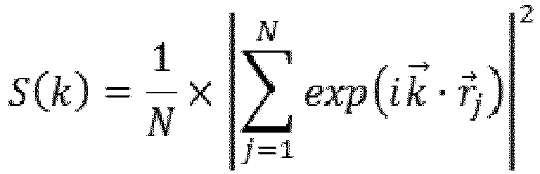
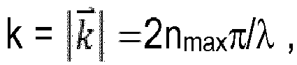
r j defines the position of the center of each aperture and
said structural factor S(k) defining a value K so that wherein kmin = 2nminπ/Lmax'Lmax being defined as the largest dimension of the optical filter defined in said plane (11),k being defined between kmin and K.
 - The optical device (1) according to claim 1 wherein

- The optical device (1) according to claim 1 or claim 2, wherein

- The optical device (1) according any one of claims 1 to 3, wherein said electrically conducting membrane (10) is made of a material having a dielectric constant comprising a real part and an imaginary part, said real part being smaller than -2 and an absolute value of the ratio of the imaginary part to the real part of the dielectric constant being less than 0.1.
- The optical device (1) according to any one of claims 1 to 4, wherein at least a dielectric layer is arranged to at least one side of said electrically conductive membrane (10).
- The optical device (1) according to claim 5, wherein said dielectric layer comprises pores.
- The optical device (1) according to claim 6, wherein said pores comprise at least a portion of through-holes extending from one side of the dielectric layer to an opposite side of the dielectric layer.
- The optical device (1) according to any one of the preceding claims, wherein said electrically conducting membrane (10) is a metallic membrane.
- The optical device (1) according to any one of the preceding claims, wherein said electrically conducting membrane (10) comprises at least two different arrays of holes (13a, 13b).
- A tunable Fabry-Perot filter (50), comprising an optical device (1) according to any one of claims 1 to 9 arranged on a first surface (44) of a gap layer (40) and further comprising a reflective layer (20) arranged on a second surface (46) of the gap layer (40) opposite and parallel to said first surface (44), said reflective layer (20) comprising an array of through-holes.
- The tunable Fabry-Perot filter (50) according to claim 10, wherein the reflective layer (20) is a second electrical conducting membrane, preferably a second optical device (1) according to any one of claims 1 to 9.
- The tunable Fabry-Perot filter (50) according to claim 10, wherein the reflective layer (20) is a stack of dielectric layers.
- The tunable Fabry-Perot filter (50) according to any one of claims 10-12, wherein the gap layer (40) comprises pores.
- The tunable Fabry-Perot filter (50) according to claim 13, wherein said pores are channels (42) extending through a thickness of said gap layer (40) between said first surface (44) and the second surface (46) thereof, said channels (42) connecting the through holes (12), (22) of the first optical filter (10) and the reflecting layer(20).
- The tunable Fabry-Perot filter (50) according to any one of claims 10 to 14, wherein the gap layer (40) is an air layer.
- The tunable Fabry-Perot filter (50) according to any one of claims 10 to 14, wherein the gap layer (40) comprises at least a dielectric layer.
- The tunable Fabry-Perot filter (50) according to one of claim 10 to 16, wherein the gap layer (40) comprises portions having different thicknesses.
Priority Applications (1)
| Application Number | Priority Date | Filing Date | Title |
|---|---|---|---|
| EP16202392.3A EP3333600A1 (en) | 2016-12-06 | 2016-12-06 | Tunable optical devices and their methods of manufacturing |
Applications Claiming Priority (1)
| Application Number | Priority Date | Filing Date | Title |
|---|---|---|---|
| EP16202392.3A EP3333600A1 (en) | 2016-12-06 | 2016-12-06 | Tunable optical devices and their methods of manufacturing |
Publications (1)
| Publication Number | Publication Date |
|---|---|
| EP3333600A1 true EP3333600A1 (en) | 2018-06-13 |
Family
ID=57539034
Family Applications (1)
| Application Number | Title | Priority Date | Filing Date |
|---|---|---|---|
| EP16202392.3A Withdrawn EP3333600A1 (en) | 2016-12-06 | 2016-12-06 | Tunable optical devices and their methods of manufacturing |
Country Status (1)
| Country | Link |
|---|---|
| EP (1) | EP3333600A1 (en) |
Cited By (2)
| Publication number | Priority date | Publication date | Assignee | Title |
|---|---|---|---|---|
| CN111721412A (en) * | 2019-03-22 | 2020-09-29 | 罗伯特·博世有限公司 | Interferometer device and method for manufacturing an interferometer device |
| WO2022023185A1 (en) * | 2020-07-30 | 2022-02-03 | Interdigital Ce Patent Holdings, Sas | Optical component and image sensor comprising an optical component |
Citations (3)
| Publication number | Priority date | Publication date | Assignee | Title |
|---|---|---|---|---|
| US20100044585A1 (en) * | 2006-10-31 | 2010-02-25 | Klunder Derk J W | Biosensor using wire-grids for increasing cavity energy |
| EP2317372A1 (en) * | 2009-10-29 | 2011-05-04 | LG Display Co., Ltd. | Liquid crystal display device and method of fabricating the same |
| GB2528682A (en) * | 2014-07-28 | 2016-02-03 | Isis Innovation | Plasmonic filter |
-
2016
- 2016-12-06 EP EP16202392.3A patent/EP3333600A1/en not_active Withdrawn
Patent Citations (3)
| Publication number | Priority date | Publication date | Assignee | Title |
|---|---|---|---|---|
| US20100044585A1 (en) * | 2006-10-31 | 2010-02-25 | Klunder Derk J W | Biosensor using wire-grids for increasing cavity energy |
| EP2317372A1 (en) * | 2009-10-29 | 2011-05-04 | LG Display Co., Ltd. | Liquid crystal display device and method of fabricating the same |
| GB2528682A (en) * | 2014-07-28 | 2016-02-03 | Isis Innovation | Plasmonic filter |
Non-Patent Citations (2)
| Title |
|---|
| E. SHANER ET AL., PLASMONIC FILTERS, SANDIA REPORT SAND2009-5990, September 2009 (2009-09-01) |
| YIJUN TANG ET AL: "Surface Plasmon Resonance: An Introduction to a Surface Spectroscopy Technique", JOURNAL OF CHEMICAL EDUCATION, vol. 87, no. 7, 1 July 2010 (2010-07-01), US, pages 742 - 746, XP055659282, ISSN: 0021-9584, DOI: 10.1021/ed100186y * |
Cited By (4)
| Publication number | Priority date | Publication date | Assignee | Title |
|---|---|---|---|---|
| CN111721412A (en) * | 2019-03-22 | 2020-09-29 | 罗伯特·博世有限公司 | Interferometer device and method for manufacturing an interferometer device |
| WO2022023185A1 (en) * | 2020-07-30 | 2022-02-03 | Interdigital Ce Patent Holdings, Sas | Optical component and image sensor comprising an optical component |
| CN116075938A (en) * | 2020-07-30 | 2023-05-05 | 交互数字Ce专利控股有限公司 | Optical component and image sensor including optical component |
| US12575203B2 (en) | 2020-07-30 | 2026-03-10 | Interdigital Ce Patent Holdings, Sas | Optical component and image sensor comprising an optical component |
Similar Documents
| Publication | Publication Date | Title |
|---|---|---|
| EP3617757B1 (en) | Optical filter, optical filter system, spectrometer and method of fabrication thereof | |
| EP1411377B1 (en) | Wire grid polarizer | |
| US6754006B2 (en) | Hybrid metallic-dielectric grating | |
| US7139459B2 (en) | Spectral filter for green and longer wavelengths | |
| Mateus et al. | Broad-band mirror (1.12-1.62 μm) using a subwavelength grating | |
| JP5490116B2 (en) | Hybrid guided-mode resonant filter and method using distributed Bragg reflection | |
| US20210080631A1 (en) | System and method for optical filtering | |
| JP4800437B2 (en) | Broadband wire grid polarizer for the visible spectrum | |
| US6274293B1 (en) | Method of manufacturing flexible metallic photonic band gap structures, and structures resulting therefrom | |
| US7158302B2 (en) | Wire grid polarizer with double metal layers | |
| US9052454B2 (en) | Spectral band-pass filter having high selectivity and controlled polarization | |
| CN103197365B (en) | Based on the plasmon spectral absorption device of periodic chirp structure | |
| Zhao et al. | 2-D terahertz metallic photonic crystals in parallel-plate waveguides | |
| US20110085232A1 (en) | Multi-spectral filters, mirrors and anti-reflective coatings with subwavelength periodic features for optical devices | |
| KR102296101B1 (en) | Spectral filter with controllable spectral bandwidth and resolution | |
| US6014251A (en) | Optical filters based on uniform arrays of metallic waveguides | |
| US20100091369A1 (en) | Double-layer grating | |
| CN103064141A (en) | Terahertz band-pass filter | |
| US20190018188A1 (en) | Optical filter and optical device using the same | |
| US8829633B2 (en) | Self-aligned semiconductor ridges in metallic slits as a platform for planar tunable nanoscale resonant photodetectors | |
| US12320997B2 (en) | Optical filtering device | |
| US6825982B1 (en) | Strongly-refractive one-dimensional photonic crystal prisms | |
| US11543571B2 (en) | Angle- and polarization-insensitive narrow-band optical filters using resonant cavities | |
| US6813080B2 (en) | Metal-free gratings for wavelength-multiplexed optical communications | |
| Joshi et al. | Multiband, continuously tunable filter in 100–300 GHz range using a two-layer cavity of perforated, all-dielectric metasurfaces |
Legal Events
| Date | Code | Title | Description |
|---|---|---|---|
| PUAI | Public reference made under article 153(3) epc to a published international application that has entered the european phase |
Free format text: ORIGINAL CODE: 0009012 |
|
| STAA | Information on the status of an ep patent application or granted ep patent |
Free format text: STATUS: THE APPLICATION HAS BEEN PUBLISHED |
|
| AK | Designated contracting states |
Kind code of ref document: A1 Designated state(s): AL AT BE BG CH CY CZ DE DK EE ES FI FR GB GR HR HU IE IS IT LI LT LU LV MC MK MT NL NO PL PT RO RS SE SI SK SM TR |
|
| AX | Request for extension of the european patent |
Extension state: BA ME |
|
| STAA | Information on the status of an ep patent application or granted ep patent |
Free format text: STATUS: REQUEST FOR EXAMINATION WAS MADE |
|
| 17P | Request for examination filed |
Effective date: 20181206 |
|
| RBV | Designated contracting states (corrected) |
Designated state(s): AL AT BE BG CH CY CZ DE DK EE ES FI FR GB GR HR HU IE IS IT LI LT LU LV MC MK MT NL NO PL PT RO RS SE SI SK SM TR |
|
| STAA | Information on the status of an ep patent application or granted ep patent |
Free format text: STATUS: EXAMINATION IS IN PROGRESS |
|
| 17Q | First examination report despatched |
Effective date: 20200124 |
|
| STAA | Information on the status of an ep patent application or granted ep patent |
Free format text: STATUS: THE APPLICATION IS DEEMED TO BE WITHDRAWN |
|
| 18D | Application deemed to be withdrawn |
Effective date: 20210701 |