EP3333126A1 - A method for releasing a graphene layer from a template substrate - Google Patents
A method for releasing a graphene layer from a template substrate Download PDFInfo
- Publication number
- EP3333126A1 EP3333126A1 EP17206508.8A EP17206508A EP3333126A1 EP 3333126 A1 EP3333126 A1 EP 3333126A1 EP 17206508 A EP17206508 A EP 17206508A EP 3333126 A1 EP3333126 A1 EP 3333126A1
- Authority
- EP
- European Patent Office
- Prior art keywords
- graphene layer
- template substrate
- substrate
- layer
- template
- Prior art date
- Legal status (The legal status is an assumption and is not a legal conclusion. Google has not performed a legal analysis and makes no representation as to the accuracy of the status listed.)
- Withdrawn
Links
Images


Classifications
-
- B—PERFORMING OPERATIONS; TRANSPORTING
- B32—LAYERED PRODUCTS
- B32B—LAYERED PRODUCTS, i.e. PRODUCTS BUILT-UP OF STRATA OF FLAT OR NON-FLAT, e.g. CELLULAR OR HONEYCOMB, FORM
- B32B43/00—Operations specially adapted for layered products and not otherwise provided for, e.g. repairing; Apparatus therefor
- B32B43/006—Delaminating
-
- C—CHEMISTRY; METALLURGY
- C01—INORGANIC CHEMISTRY
- C01B—NON-METALLIC ELEMENTS; COMPOUNDS THEREOF; METALLOIDS OR COMPOUNDS THEREOF NOT COVERED BY SUBCLASS C01C
- C01B32/00—Carbon; Compounds thereof
- C01B32/15—Nano-sized carbon materials
- C01B32/182—Graphene
- C01B32/194—After-treatment
-
- B—PERFORMING OPERATIONS; TRANSPORTING
- B32—LAYERED PRODUCTS
- B32B—LAYERED PRODUCTS, i.e. PRODUCTS BUILT-UP OF STRATA OF FLAT OR NON-FLAT, e.g. CELLULAR OR HONEYCOMB, FORM
- B32B15/00—Layered products comprising a layer of metal
- B32B15/04—Layered products comprising a layer of metal comprising metal as the main or only constituent of a layer, which is next to another layer of the same or of a different material
-
- B—PERFORMING OPERATIONS; TRANSPORTING
- B32—LAYERED PRODUCTS
- B32B—LAYERED PRODUCTS, i.e. PRODUCTS BUILT-UP OF STRATA OF FLAT OR NON-FLAT, e.g. CELLULAR OR HONEYCOMB, FORM
- B32B37/00—Methods or apparatus for laminating, e.g. by curing or by ultrasonic bonding
- B32B37/02—Methods or apparatus for laminating, e.g. by curing or by ultrasonic bonding characterised by a sequence of laminating steps, e.g. by adding new layers at consecutive laminating stations
- B32B37/025—Transfer laminating
-
- B—PERFORMING OPERATIONS; TRANSPORTING
- B32—LAYERED PRODUCTS
- B32B—LAYERED PRODUCTS, i.e. PRODUCTS BUILT-UP OF STRATA OF FLAT OR NON-FLAT, e.g. CELLULAR OR HONEYCOMB, FORM
- B32B9/00—Layered products comprising a layer of a particular substance not covered by groups B32B11/00 - B32B29/00
- B32B9/005—Layered products comprising a layer of a particular substance not covered by groups B32B11/00 - B32B29/00 comprising one layer of ceramic material, e.g. porcelain, ceramic tile
- B32B9/007—Layered products comprising a layer of a particular substance not covered by groups B32B11/00 - B32B29/00 comprising one layer of ceramic material, e.g. porcelain, ceramic tile comprising carbon, e.g. graphite, composite carbon
-
- C—CHEMISTRY; METALLURGY
- C01—INORGANIC CHEMISTRY
- C01B—NON-METALLIC ELEMENTS; COMPOUNDS THEREOF; METALLOIDS OR COMPOUNDS THEREOF NOT COVERED BY SUBCLASS C01C
- C01B32/00—Carbon; Compounds thereof
- C01B32/15—Nano-sized carbon materials
- C01B32/182—Graphene
- C01B32/184—Preparation
-
- C—CHEMISTRY; METALLURGY
- C07—ORGANIC CHEMISTRY
- C07F—ACYCLIC, CARBOCYCLIC OR HETEROCYCLIC COMPOUNDS CONTAINING ELEMENTS OTHER THAN CARBON, HYDROGEN, HALOGEN, OXYGEN, NITROGEN, SULFUR, SELENIUM OR TELLURIUM
- C07F7/00—Compounds containing elements of Groups 4 or 14 of the Periodic Table
- C07F7/02—Silicon compounds
- C07F7/08—Compounds having one or more C—Si linkages
- C07F7/0803—Compounds with Si-C or Si-Si linkages
- C07F7/081—Compounds with Si-C or Si-Si linkages comprising at least one atom selected from the elements N, O, halogen, S, Se or Te
-
- C—CHEMISTRY; METALLURGY
- C07—ORGANIC CHEMISTRY
- C07F—ACYCLIC, CARBOCYCLIC OR HETEROCYCLIC COMPOUNDS CONTAINING ELEMENTS OTHER THAN CARBON, HYDROGEN, HALOGEN, OXYGEN, NITROGEN, SULFUR, SELENIUM OR TELLURIUM
- C07F7/00—Compounds containing elements of Groups 4 or 14 of the Periodic Table
- C07F7/02—Silicon compounds
- C07F7/08—Compounds having one or more C—Si linkages
- C07F7/10—Compounds having one or more C—Si linkages containing nitrogen having a Si-N linkage
-
- C—CHEMISTRY; METALLURGY
- C25—ELECTROLYTIC OR ELECTROPHORETIC PROCESSES; APPARATUS THEREFOR
- C25F—PROCESSES FOR THE ELECTROLYTIC REMOVAL OF MATERIALS FROM OBJECTS; APPARATUS THEREFOR
- C25F5/00—Electrolytic stripping of metallic layers or coatings
-
- H—ELECTRICITY
- H10—SEMICONDUCTOR DEVICES; ELECTRIC SOLID-STATE DEVICES NOT OTHERWISE PROVIDED FOR
- H10P—GENERIC PROCESSES OR APPARATUS FOR THE MANUFACTURE OR TREATMENT OF DEVICES COVERED BY CLASS H10
- H10P90/00—Preparation of wafers not covered by a single main group of this subclass, e.g. wafer reinforcement
- H10P90/19—Preparing inhomogeneous wafers
- H10P90/1904—Preparing vertically inhomogeneous wafers
-
- H—ELECTRICITY
- H10—SEMICONDUCTOR DEVICES; ELECTRIC SOLID-STATE DEVICES NOT OTHERWISE PROVIDED FOR
- H10P—GENERIC PROCESSES OR APPARATUS FOR THE MANUFACTURE OR TREATMENT OF DEVICES COVERED BY CLASS H10
- H10P90/00—Preparation of wafers not covered by a single main group of this subclass, e.g. wafer reinforcement
- H10P90/21—Preparation of wafers not covered by a single main group of this subclass, e.g. wafer reinforcement by transferring two-dimensional materials
- H10P90/212—Preparation of wafers not covered by a single main group of this subclass, e.g. wafer reinforcement by transferring two-dimensional materials by transferring of graphene
-
- B—PERFORMING OPERATIONS; TRANSPORTING
- B32—LAYERED PRODUCTS
- B32B—LAYERED PRODUCTS, i.e. PRODUCTS BUILT-UP OF STRATA OF FLAT OR NON-FLAT, e.g. CELLULAR OR HONEYCOMB, FORM
- B32B2311/00—Metals, their alloys or their compounds
- B32B2311/02—Noble metals
- B32B2311/06—Platinum
-
- B—PERFORMING OPERATIONS; TRANSPORTING
- B32—LAYERED PRODUCTS
- B32B—LAYERED PRODUCTS, i.e. PRODUCTS BUILT-UP OF STRATA OF FLAT OR NON-FLAT, e.g. CELLULAR OR HONEYCOMB, FORM
- B32B37/00—Methods or apparatus for laminating, e.g. by curing or by ultrasonic bonding
-
- B—PERFORMING OPERATIONS; TRANSPORTING
- B32—LAYERED PRODUCTS
- B32B—LAYERED PRODUCTS, i.e. PRODUCTS BUILT-UP OF STRATA OF FLAT OR NON-FLAT, e.g. CELLULAR OR HONEYCOMB, FORM
- B32B37/00—Methods or apparatus for laminating, e.g. by curing or by ultrasonic bonding
- B32B37/14—Methods or apparatus for laminating, e.g. by curing or by ultrasonic bonding characterised by the properties of the layers
- B32B37/16—Methods or apparatus for laminating, e.g. by curing or by ultrasonic bonding characterised by the properties of the layers with all layers existing as coherent layers before laminating
- B32B37/18—Methods or apparatus for laminating, e.g. by curing or by ultrasonic bonding characterised by the properties of the layers with all layers existing as coherent layers before laminating involving the assembly of discrete sheets or panels only
-
- B—PERFORMING OPERATIONS; TRANSPORTING
- B32—LAYERED PRODUCTS
- B32B—LAYERED PRODUCTS, i.e. PRODUCTS BUILT-UP OF STRATA OF FLAT OR NON-FLAT, e.g. CELLULAR OR HONEYCOMB, FORM
- B32B38/00—Ancillary operations in connection with laminating processes
- B32B38/10—Removing layers, or parts of layers, mechanically or chemically
-
- B—PERFORMING OPERATIONS; TRANSPORTING
- B81—MICROSTRUCTURAL TECHNOLOGY
- B81C—PROCESSES OR APPARATUS SPECIALLY ADAPTED FOR THE MANUFACTURE OR TREATMENT OF MICROSTRUCTURAL DEVICES OR SYSTEMS
- B81C1/00—Manufacture or treatment of devices or systems in or on a substrate
-
- C—CHEMISTRY; METALLURGY
- C01—INORGANIC CHEMISTRY
- C01B—NON-METALLIC ELEMENTS; COMPOUNDS THEREOF; METALLOIDS OR COMPOUNDS THEREOF NOT COVERED BY SUBCLASS C01C
- C01B2204/00—Structure or properties of graphene
- C01B2204/02—Single layer graphene
-
- Y—GENERAL TAGGING OF NEW TECHNOLOGICAL DEVELOPMENTS; GENERAL TAGGING OF CROSS-SECTIONAL TECHNOLOGIES SPANNING OVER SEVERAL SECTIONS OF THE IPC; TECHNICAL SUBJECTS COVERED BY FORMER USPC CROSS-REFERENCE ART COLLECTIONS [XRACs] AND DIGESTS
- Y02—TECHNOLOGIES OR APPLICATIONS FOR MITIGATION OR ADAPTATION AGAINST CLIMATE CHANGE
- Y02P—CLIMATE CHANGE MITIGATION TECHNOLOGIES IN THE PRODUCTION OR PROCESSING OF GOODS
- Y02P20/00—Technologies relating to chemical industry
- Y02P20/50—Improvements relating to the production of bulk chemicals
- Y02P20/582—Recycling of unreacted starting or intermediate materials
-
- Y—GENERAL TAGGING OF NEW TECHNOLOGICAL DEVELOPMENTS; GENERAL TAGGING OF CROSS-SECTIONAL TECHNOLOGIES SPANNING OVER SEVERAL SECTIONS OF THE IPC; TECHNICAL SUBJECTS COVERED BY FORMER USPC CROSS-REFERENCE ART COLLECTIONS [XRACs] AND DIGESTS
- Y10—TECHNICAL SUBJECTS COVERED BY FORMER USPC
- Y10T—TECHNICAL SUBJECTS COVERED BY FORMER US CLASSIFICATION
- Y10T156/00—Adhesive bonding and miscellaneous chemical manufacture
- Y10T156/11—Methods of delaminating, per se; i.e., separating at bonding face
-
- Y—GENERAL TAGGING OF NEW TECHNOLOGICAL DEVELOPMENTS; GENERAL TAGGING OF CROSS-SECTIONAL TECHNOLOGIES SPANNING OVER SEVERAL SECTIONS OF THE IPC; TECHNICAL SUBJECTS COVERED BY FORMER USPC CROSS-REFERENCE ART COLLECTIONS [XRACs] AND DIGESTS
- Y10—TECHNICAL SUBJECTS COVERED BY FORMER USPC
- Y10T—TECHNICAL SUBJECTS COVERED BY FORMER US CLASSIFICATION
- Y10T156/00—Adhesive bonding and miscellaneous chemical manufacture
- Y10T156/19—Delaminating means
Definitions
- the present inventive concept relates to methods for releasing a graphene layer from a template substrate.
- One or more graphene layers may be formed on a template substrate, for instance by chemical vapor deposition (CVD).
- CVD chemical vapor deposition
- the graphene layer(s) are then to be released or delaminated from the template substrate and transferred to a target substrate.
- EP 2 719 797 discloses a graphene transfer method wherein graphene is synthesized on an initial substrate. The graphene is released from the substrate using an electrolysis process. The released graphene is subsequently bonded to a target substrate.
- An objective of the present inventive concept is to provide an improved method for releasing a graphene layer from a template substrate, enabling more reliable separation of the graphene layer. Additional or alternative objectives may be understood from the following.
- a method for releasing a graphene layer from a template substrate on which the graphene layer is provided comprising:
- soaking the graphene layer and the template substrate in liquid phase water such that water is intercalated between the template substrate and the graphene layer enables a more reliable separation, i.e. delamination, of the graphene layer from the template substrate.
- the intercalated water between the template substrate and the graphene layer allows separation by applying a smaller separation force to the graphene layer and the template substrate during the delamination process compared to the prior art.
- the intercalated water also reduces risk of damaging graphene layer during the delamination process.
- delamination process is hereby meant a process adapted to drive a release of the graphene layer from the template substrate.
- the graphene layer may be bonded to the template substrate by adhesion.
- the graphene layer may be bonded to the template substrate by Van der Waal forces.
- the delamination process is in other words a process adapted to break the bonding between the graphene layer and the template substrate.
- the process may include supplying energy to the graphene layer and the template substrate in a form driving the release of the graphene layer from the template substrate.
- Advantageous delamination process will be further described below and may include supplying the energy by means of bubble formation in a liquid, electrolysis and/or ultrasound.
- intercalation of water between the template substrate and the graphene layer is hereby meant a process wherein the water (in which the graphene layer and the template substrate is submerged) enters between the graphene layer and the template substrate.
- the intercalated water may form one to a few (mono-)layers of water.
- the intercalated water may also be referred to as interfacial water (IFW).
- the soaking may be of a duration allowing intercalated water to form along at least a sufficient portion of the interface between the graphene layer and the template layer.
- a sufficient portion may here be understood as a portion which is sufficient for allowing separation of the graphene layer from the template substrate with no or a minimum risk of damaging the graphene layer.
- the soaking may be of a duration allowing intercalated water to form along a major portion of the interface between the graphene layer and the template layer. More preferably, the soaking may be of a duration allowing intercalated water to form along the entire interface between the graphene layer and the template layer. This may facilitate releasing the graphene layer from the template substrate.
- the graphene layer and the template substrate are subjected to the water treatment by soaking for a predetermined duration prior to initiating the delamination process.
- intercalated water may be formed between the graphene layer and the template layer prior to subjecting the graphene layer and the template layer to the conditions of the delamination process. This may improve the overall efficiency of the separation method and reduce the risk of damaging the graphene layer.
- the graphene layer and the template layer may be subjected to the delamination process at a reduced power (e.g. a lower rate of bubble formation, a lower bias driving the electrolysis, reduced power of the ultrasound).
- a reduced power e.g. a lower rate of bubble formation, a lower bias driving the electrolysis, reduced power of the ultrasound.
- the graphene layer and the template substrate may be subjected to the water treatment by soaking for a predetermined duration of at least 1 hour.
- An extended duration of the soaking enables intercalation of water along a greater portion of the interface between the graphene layer and the template substrate.
- an extended duration enables intercalation of water along the entire interface between the graphene layer and the template layer also for graphene layers of increased lateral/in-plane dimensions.
- the water may be heated to a temperature of at least 30 °C, at least 50 °C, or at least 80 °C. Heating the liquid phase water provides thermal energy which may accelerate the intercalation process. An overall time efficiency of the separation method may thereby be improved.
- the water is preferably heated to a temperature below the boiling point. Bubble formation prior to a sufficient water intercalation has occurred may thereby be avoided.
- the water treatment may include soaking the graphene layer and the template substrate by submerging the graphene layer in the liquid phase water.
- the method may further include transferring and bonding of the graphene layer to a target substrate.
- the method further comprises:
- This method does not require any additional temporary handling wafer between the delamination process and the transfer and bonding. Obviating the need of a temporary additional handling wafer reduces the risk of contaminating the graphene layer during processing relating to bonding and release from such a temporary wafer.
- the method also enables reuse of the template substrate.
- the transfer may be performed prior to or subsequent to the water treatment.
- a bonding process for bonding the graphene layer to the target substrate may be performed prior to the water treatment.
- the bonding process may alternatively be performed subsequent to the water treatment.
- the bonding process may alternatively be performed with an overlap with respect to the water treatment. Accordingly, the bonding may be achieved during the water treatment.
- the transfer includes forming of a stack including the target substrate, the graphene layer and the template substrate.
- the graphene layer and the target substrate may be bonded by dry bonding. Hence no intermediate layers are needed between the graphene layer and the hydrophobic surface of the target substrate.
- the graphene layer may be bonded by applying a pressure to press the graphene layer against the target substrate.
- the graphene layer may be bonded to a hydrophobic surface of the target substrate. By virtue of the hydrophobic surface of the target substrate, water intercalation between the target substrate and the graphene layer may be counteracted.
- the hydrophobic surface may be formed by a self-assembled monolayer (SAM) on the target substrate.
- SAM self-assembled monolayer
- the SAM may include a hydrophobic terminal group or tail group.
- the head group of the SAM may be selected to allow bonding thereof to the target substrate.
- This embodiment allows a graphene layer to be transferred and bonded to a target substrate.
- the carrier layer allows protection of the second surface of the graphene layer during the delamination process.
- the carrier layer may further reduce the risk of cracking or folding of the graphene layer during the delamination.
- the carrier layer may also act as protection for the graphene layer and facilitate handling of the graphene layer after the delamination process, for instance during the transfer of the graphene layer to the target substrate.
- the forming of the carrier layer may be performed prior to or subsequent to said water treatment.
- the carrier layer may be removed from the second surface, wherein the graphene layer remains on the target substrate.
- the transfer includes forming of a stack including the target substrate and the graphene layer. Subsequent to forming the carrier layer, also the carrier layer forms part of the stack.
- the graphene layer and the target substrate may be bonded by dry bonding. Hence no intermediate layers are needed between the graphene layer and the target substrate.
- the graphene layer may be bonded by applying a pressure to press the graphene layer against the target substrate.
- the carrier layer may be a spin-coated organic layer.
- the carrier layer may be a spin-coated polymer-including layer. Spin-coating allows controlled forming of a carrier layer as a thin film with good coverage and a high degree of thickness control.
- the delamination process may include submerging the template substrate and the graphene layer in a liquid and forming bubbles at the interface between the template substrate and the graphene layer. Bubbles forming at the interface may drive the release of the graphene layer from the template substrate.
- the delamination process may include subjecting the template substrate and the graphene layer to electrolysis. Electrolysis allows convenient and accurate control of the resulting separation forces between the template substrate and the graphene layer by controlling the bias applied across the electrodes. By the electrolysis bubbles may form at the interface between the graphene layer and the template substrate.
- the template substrate and the graphene layer may be submerged in a liquid forming an electrolyte.
- a bias may be applied by a voltage source across a first electrode and a second electrode submerged in the liquid.
- the delamination process may include subjecting the template substrate and the graphene layer to ultrasound. By the resulting pressure waves bubbles may form at the interface between the graphene layer and the template substrate.
- the template substrate and the graphene layer may be submerged in a liquid. Ultrasonic signals may be induced in the liquid. The ultrasonic signals may be ultrasonic pulses.
- the liquid in which the graphene layer and the template substrate may be submerged during the delamination process may be formed by the water used in the water treatment.
- the water in which the graphene layer and the template substrate are soaked such that that water is intercalated between the template substrate and the graphene layer may be formed by the water used in the water treatment.
- the water treatment and the delamination process need not be performed at different and physically separate processing equipment but may be performed at a same location. For instance, the water treatment and the delamination process may be performed in a same water-including container or tank.
- the graphene layer may be grown on the template substrate.
- the template substrate may also be referred to as a growth substrate.
- Graphene layer may be epitaxially grown on the template substrate.
- the graphene layer may be grown by CVD.
- the surface of the template substrate on which the graphene layer is provided may be formed by a transition metal, an alloy of transition metals, a group III element or a group IV element. There exist growth processes enabling forming of high-quality graphene layers on such template substrates.
- the surface of the template substrate may be formed by Platinum (Pt).
- Pt is an advantageous material for CVD-based graphene growth and allows high quality growth of both monolayer graphene and millimeter-sized graphene islands.
- Pt has a comparably low tendency to oxidize during the water treatment. Oxidization may otherwise reduce the rate at which intercalation occurs during the water treatment.
- Pt also allows the template substrate to be used as an electrode during an electrolysis-based delamination process.
- the template substrate may include a growth layer on which the graphene layer is provided and a support layer on which the growth layer is arranged.
- the growth layer may be formed of any of the aforementioned materials and with a thickness on the order of nanometers to hundreds of nanometers.
- the growth layer may be formed by a foil any of the aforementioned materials.
- the support layer may support the growth layer.
- the support layer may be a sapphire layer.
- the support layer may be an MgO layer.
- the support layer may be a stack of a Si-layer and an MgO-layer.
- the support layer may be an Al 2 O 3 -layer.
- Such support layers enable template substrates with a surface (i.e. of the growth layer) of 111-, 100- and 110-orientation.
- intercalation between a graphene layer and a template substrate
- other liquids than water may enable a more reliable separation, i.e. delamination, of the graphene layer from the template substrate, compared to prior art approaches.
- a method for releasing a graphene layer from a template substrate on which the graphene layer is provided comprising:
- the liquid treatment may advantageously be a water treatment wherein the liquid may be liquid phase water.
- the liquid may more generally be a liquid of molecules with a dipole moment and having a molecular size comparable to that of water.
- the liquid may be (liquid phase) chloroform.
- the chloroform may intercalate between the template substrate and the graphene layer. This enables a more reliable separation, i.e. delamination, of the graphene layer from the template substrate.
- the graphene layer and the template substrate may be subjected to the liquid treatment for a predetermined duration of at least 1 hour.
- the liquid may be heated (e.g. to a temperature above room temperature but below the boiling point of the liquid) to accelerate the intercalation process.
- the graphene layer may further be transferred to a target substrate according to any of the above described embodiments.
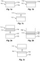
- a method for releasing a graphene layer 114 from a template substrate 112 will to be described with reference to Fig. 1a-c .
- Fig. 1 a illustrates the graphene layer 114 provided on the template substrate 112.
- the template substrate 112 may include a support layer 112a and a growth layer 112b.
- the growth layer 112b forms the main surface of the template substrate 112 on which the graphene layer 114 is provided.
- the growth layer 112b is arranged on the support layer 112a.
- the growth layer 112b may be formed by a foil of a transition metal, for instance Pt, Cu, Ir or Ni.
- the support layer 112a may be a sapphire layer.
- the support layer 112a may be an MgO layer.
- the support layer 112a may be a stack of a Si-layer and an MgO-layer.
- the support layer 112a may be a Al 2 O 3 -layer.
- the growth layer 112b may be formed with a 111-, 100- or 110-orientation on the support layer 112a. In applications wherein no particular crystallinity is required the support layer 112b may also be a stack of a Si-layer and a SiO 2 -layer.
- a template substrate may be formed by a group III or group IV semiconductor substrate.
- examples include a template substrate of a stack of Si(111)/Ge(111), a stack of Si(100)/Ge(100), a bulk Ge wafer or a stack of Sapphire(0001)/GaN.
- the surface of the template substrate 112 on which the graphene layer 114 is provided represents a main surface of the template substrate 112.
- the main surface of the template substrate 112 may be referred to as a first or upper surface of the template substrate 112.
- the main surface of the template substrate 112 is formed by the growth layer 112b.
- the surface of the graphene layer 114 facing away from template substrate 112 represents a first main surface of the graphene layer 114.
- the first main surface of the graphene layer 114 may be referred to as a first surface of the graphene layer 114.
- the surface of the graphene layer 114 facing the template substrate 112 represents a second main surface of the graphene layer 114.
- the second main surface of the graphene layer 114 may be referred to as a second surface of the graphene layer 114.
- the drawings show the layer structures in mere schematic manner.
- the dimension of the various layers, in particular the relative thickness of the layers as illustrated may differ from a physical structure.
- the lateral dimensions of the template substrate 112 may typically be greater than those of the graphene layer 114 such that one or more graphene layers are formed on only portions of main surface of the template substrate 112.
- the graphene layer 114 may be epitaxially grown on the main surface of the template substrate 112 in a CVD process, in a manner which per se is known in the art.
- the growth layer 112b may act as a catalyst during the CVD process.
- Other options include epitaxially growing a graphene layer by heating a SiC template substrate.
- the method comprises subjecting the graphene layer 114 and the template substrate 112 to a water treatment by soaking the graphene layer 114 and the template substrate 112 in water.
- a water treatment by soaking the graphene layer 114 and the template substrate 112 in water.
- the result of the water treatment is illustrated in Fig. 1b wherein interfacial water 116 is intercalated between the template substrate 112 and the graphene layer 114.
- the stack including the graphene layer 114 and the template substrate 112 may be submerged in water in a container or tank (not shown).
- the water used in the water treatment may be de-ionized water.
- the water may be ultra-pure water. De-ionized, and to an even greater extent, ultra-pure water may result in a reduced occurrence of contaminations on the graphene layer 114.
- the water may however also be an aqueous solution.
- the solution may include dissolved salt.
- the water may be aqueous NaCl, NaOH or KOH.
- a compound dissolved in the water may accelerate the intercalation process. For instance, the organization of the water molecules around dissolved ions (such as Na+ or K+) may facilitate the intercalation process.
- the graphene layer 114 and the template substrate 112 may be submerged in the water for a duration which is sufficient for allowing intercalated water to form along at least a sufficient portion of the interface between the graphene layer 114 and the template layer 112.
- the minimum duration for this to occur may be dependent on factors such as the dimensions of the graphene layer 114, the particular composition of the water and the temperature of the water.
- the minimum duration required to obtain a sufficient degree of interfacial water 116 may be determined by trial and error. For instance, by submerging a sample stack including a graphene layer 114 and a template substrate 112 for gradually increasing durations and inspecting the stack, e.g. by scanning electron microscopy (SEM), to determine the presence of interfacial water 116
- intercalated interfacial water may be distinguished from water adsorbed to the main surface of the graphene layer 114 facing away from the template substrate 112 since adsorbed water is typically removed by an annealing process, whereas intercalated interfacial water is typically not.
- the stack may be inspected by SEM after subjecting the stack to an anneal step, for instance at 500 °C for an hour or longer.
- the predetermined minimum duration may be used for water treatment of stacks including a graphene layer 114 and a template substrate 112 of a configuration corresponding to that of the sample stack.
- the graphene layer 114 and the template substrate 112 may be subjected to the water treatment by soaking for a predetermined duration of at least 1 hour.
- the water may be heated to a temperature above room temperature.
- the water may be heated by heating coils arranged in the tank or an immersion heater.
- the water may be heated to a temperature of at least 30 °C, at least 50 °C, or at least 80 °C.
- An elevated water temperature may allow a sufficient amount of intercalated water to form between the graphene layer 114 and the template substrate 112 in a time span even shorter than 1 hour.
- the graphene layer 114 is grown to present an in-plane / lateral dimension on the order of only one to a few millimeters, or less than one millimeter.
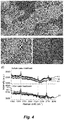
- FIG. 4a A SEM image of a Pt foil/graphene layer sample stack immediately after growth is shown in Fig. 4a .
- the observed color contrast corresponds mainly to different Pt grain orientations, which is related to an electron channeling contrast.
- the electron channeling contrast is formed as a result of electron backscattering effects which occur in a thin layer at the sample surface, which makes it a surface sensitive technique.
- elastic scattering effects decollimate the electron beam and inelastic scattering reduces the energy of the electrons.
- the initially highly collimated beam which is sensitive to the orientation of the Pt grains, is decollimated.
- Fig. 4d shows the results of Raman spectroscopy measurements performed immediately after graphene growth is (shown on top) and after the water treatment (shown below). Three measurements M1, M2, M3 were performed at different locations of the graphene layer before and after the water treatment. The width of the Raman spot was approximately 1 ⁇ m. In each of the measurements, the three pronounced peaks are visible, namely the D, G, and 2D peak. The D-peak, also called defect peak, is only present when the graphene layer is defective. The G and 2D peak corresponds with oscillations of the carbon atoms in the graphene sheet.
- the peak position, the full width half maximum and the peak ratios give information of graphene layer thickness (number of graphene layers), doping level of the graphene sheet, strain in the layer, stacking of the layers etc.
- the Raman spectroscopy shows a clear blue shift of the G and 2D peaks.
- the small additional Raman peak at 2328 cm -1 is coming from N 2 present in air.
- the results show that after the water treatment, graphene is still present on the surface, but IFW is intercalated between the Pt foil and the graphene layer. Similar results have been obtained with a duration of the water treatment of about 3 hours with a water temperature of 80 °C.
- the graphene layer 114 and the template substrate 112 are subjected to a delamination process. As schematically illustrated, the graphene layer 114 is thereby released and separated from the template substrate 112. Following the delamination process the graphene layer 114 may be transferred to a target substrate as will be further described below.
- the delamination process may include subjecting the template substrate 112 and the graphene layer 114 to electrolysis.
- the template substrate 112 and the graphene layer 114 may be submerged in a liquid forming an electrolyte.
- the electrolyte may be an NaCl, NaOH or KOH solution.
- the concentration of the solution may be in the range of 0.05 to 5 M.
- the temperature of the electrolyte may be room temperature (e.g. 20 °C) or above.
- a bias may be applied by a voltage source across a first electrode and a second electrode submerged in the liquid. If the template substrate 112 includes a conductor (such as Pt) the template substrate 112 may be connected to the voltage source and act as a first electrode.
- a DC bias in the range of 1-20 V may be applied. The DC bias may be applied until the graphene layer 114 has been delaminated from the template substrate 112. The DC bias may be applied for a duration in the range of few seconds to one or a few minutes, depending on for instance the magnitude of the DC bias.
- the electrolysis results in an electrochemical reaction wherein bubbles of O 2 and H 2 form in the electrolyte. Especially, bubbles form at the interface between the graphene layer 114 and the template substrate 112. The interfacial bubbles may cause the template substrate 112 and the graphene layer 114 to eventually release from each other.
- the delamination process may alternatively include subjecting the template substrate 112 and the graphene layer 114 to ultrasound.
- the stack including the template substrate 112 and the graphene layer 114 may be submerged in a liquid.
- Ultrasonic signals may be induced in the liquid by an ultrasonic transducer.
- the ultrasonic signals may be ultrasonic pulses.
- ultrasonic signals of a frequency between 30 kHz and 2 MHz may be applied for a duration of a few seconds to 30 minutes.
- the stack including the template substrate 112 and the graphene layer 114 may be subjected to the ultrasound treatment until the graphene layer 114 has been delaminated from the template substrate 112.
- Ultrasonic waves in the liquid medium will when incident on the graphene layer 114 and the template substrate 112 impart a momentum which may cause the template substrate 112 and the graphene layer 114 to be released from each other. Additionally, during a low pressure period of the soundwave, (vapor) bubbles may form at the interface between the graphene layer 114 and the template substrate 112. These bubbles may also contribute to separation of the template substrate 112 and the graphene layer 114.
- the stack including the template substrate 112 and the graphene layer 114 may be submerged in NH 4 OH/H 2 O 2 /H 2 O or in heated ammonium peroxide.
- the stack including the template substrate 112 and the graphene layer 114 may be submerged in boiling water.
- the water treatment and the delamination process may be performed in different containers or tanks.
- the stack including the template substrate 112 and the graphene layer 114 may accordingly be transferred from a first tank (for the water treatment) to a second tank, different from the first tank, (for the delamination process). It is however also possible to perform the water treatment and the delamination process in a same tank. If liquids with different properties are to be used in the water treatment and the delamination process (for instance if de-ionized or ultrapure water is to be used in the water treatment) the water may be evacuated from the tank following the water treatment and filled with another liquid (e.g. an electrolyte) before the delamination process is initiated.
- another liquid e.g. an electrolyte
- Fig. 2a-c schematically illustrates a method for releasing the graphene layer 114 from the template substrate 112 and directly transferring and bonding the graphene layer 114 to a target substrate 120.
- a stack including the graphene layer 114, the template substrate 112 and intercalated water 116 forming IFW between the graphene layer 114 and the template substrate 112 is transferred to the target substrate 120.
- the state of the stack hence corresponds to what was described in connection with Fig. 1b above. Accordingly, the template substrate 112 and the graphene layer 114 are transferred to the target substrate 120 subsequent to the water treatment.
- the target substrate 120 may be a semiconductor substrate.
- the target substrate 120 may be a Si-substrate.
- a silicon oxide layer may be arranged on the Si-substrate.
- the target substrate 120 may be a bulk semiconductor substrate, a group IV semiconductor substrate (e.g. a Si-substrate or a Ge-substrate), a group III-V semiconductor substrate (e.g.
- a GaAs-substrate an InGaAs-substrate, an InP-substrate
- SOI silicon-on-insulator
- SiOI germanium-on-insulator-substrate
- Partially completed devices of which the graphene layer 114 may form part may be present on the target substrate 120.
- the graphene layer 114 may also be arranged as an interconnect between already completed devices on the target substrate 120.
- the target substrate 120 may as shown be provided with a hydrophobic surface in the form of a SAM 122.
- the SAM 112 may be formed by vapor deposition in a manner which per se is known in the art.
- the SAM may be a layer of perfluorodecyltrichlorosilane (FDTS).
- FDTS perfluorodecyltrichlorosilane
- the terminal or tail group of a FDTS SAM is hydrophobic.
- the head group of a FDTS SAM allows bonding to a silicon oxide layer on a Si-substrate (or to a corresponding oxide layer if the target substrate 120 is formed by another semiconductor).
- An FDTS SAM is however only an example and any SAM with a hydrophobic tail group and a head group allowing bonding thereof to the target substrate 112 is possible, for instance octadecyltrichlorosilane (ODTS) and hexamethyldisilazane (HMDS).
- ODTS octadecyltrichlorosilane
- HMDS hexamethyldisilazane
- the hydrophobic surface need not even be provided by a SAM.
- a target substrate 120 of Si may be provided by a hydrophobic SiO 2 This can be obtained by a short dilute HF dip, or by an oven oxidation of Si.
- the stack including the template substrate 112 and the graphene layer 114 is subjected to a bonding process, wherein the graphene layer 114 is bonded to the target substrate 120, i.e. to the hydrophobic SAM 112 thereon.
- the bonding may be achieved by a dry bonding process.
- a mechanical pressure on the order one to a few hundreds of kPa may be applied to the stack (in a normal direction to the layers of the stack). The pressure may be applied until the graphene layer 114 has bonded to the target substrate 120. The pressure may be applied for a duration in the range of one minute to one or a few tens of minutes.
- Other examples of bonding processes include vacuum bonding and anodic bonding.
- the graphene layer 114 and the template substrate 112 are subjected to the delamination process, wherein the graphene layer 114 is released from the template substrate 112. As shown in Fig. 2c , the graphene layer 114 and the template substrate 112 may thereafter be separated from each other while the graphene layer 114 remains bonded to the target substrate 120.
- the hydrophobic surface of the target substrate 120 provided by the SAM 122 water intercalation between the target substrate 120 and the graphene layer 114 during the water treatment may be counteracted.
- the stack including the graphene layer 114 and the template substrate may, directly following the growth process, be transferred to the target substrate 120.
- the bonding process may thereafter be performed wherein the graphene layer 114 is bonded to the target substrate 120.
- the stack including the target substrate 120, the SAM 122 (if present), the graphene layer 114 and the template substrate 112 may be soaked in water such that water is intercalated between the template substrate 112 and the graphene layer 114, as described above.
- the delamination process may be performed, causing the release of the graphene layer 114 from the template substrate 112.
- the bonding process may even be performed during (i.e. at least partially overlap with) the water treatment.
- a mechanical pressure may be applied to the stack including the target substrate 120, the SAM 120 (if present), the graphene layer 114 and the template substrate 112, while the stack is being soaked.
- the delamination process may be performed during (i.e. at least partially overlap with) the bonding process.
- a mechanical pressure may be applied to the stack including the target substrate 120, the SAM 120 (if present), the graphene layer 114 and the template substrate 112, while the delamination process, for instance by electrolysis, is performed.
- the mechanical pressure may for instance be released after completion of the electrolysis.
- Fig. 5a-c shows SEM and AFM (atomic force microscope) measurements after a graphene layer has been transferred and bonded to a target substrate.
- a first step an Al 2 O 3 /Pt/graphene layer sample stack was immersed in ultra-pure water at 50 °C for 16 h to achieve water intercalation between the graphene layer and the Pt(111) surface.
- a Si/SiO 2 target substrate coated with a FDTS SAM was bonded to the Al 2 O 3 /Pt(111)/IFW/graphene layer sample stack by applying a pressure of 200 kPa to the sample stack.
- electrolysis was performed by applying a -2.5 V voltage for 2 min to the sample stack submerged in an 0.2 M NaOH electrolyte. The aqueous NaOH was thereafter rinsed off with UPW until the pH of the solution reached 7 and finally the pressure applied to the sample stack was gradually removed.
- Fig. 5a-c illustrate the feasibility of a direct graphene layer transfer method from a template substrate to a target substrate.
- the SEM and AFM measurements shows presence of wrinkles in the graphene layer. Those wrinkles may however be attributed to the graphene growth process, since the thermal expansion coefficient of graphene and Pt are different (wrinkles appear during cool down after growth) and not to the delamination, transfer and bonding processes.
- Annealing the sample at 150 °C for 1 h in a nitrogen atmosphere decreases the 2D/G peak ratio to 1.08 ⁇ 0.11 while ⁇ 2D remains almost identical.
- graphene doping is higher likely due to stronger interaction between the FDTS SAM and the graphene.
- a lower 2D/G ratio shows a higher doping.
- the FWHM does not change significantly, so the graphene mobility is not expected to be impacted by the anneal step.
- Fig. 4-5 were obtained using a SEM (FEI Nova 200) and an AFM (Bruker Dimension Edge).
- Fig. 3a-c is a schematic illustration of a method for releasing the graphene layer 114 from the template substrate 112 and subsequently transferring and bonding the graphene layer 114 to a target substrate 120.
- Fig. 3a corresponds to the stage of the method shown in Fig. 1c wherein the graphene layer 114 has released from the template substrate 112 and been separated therefrom.
- a carrier layer 130 is formed on the first surface of the graphene layer 114 facing away from the template substrate 112.
- the carrier layer 130 may be formed either prior to or subsequent to the water treatment.
- the carrier layer 130 may be a polymer-including layer.
- the carrier layer 130 may be a spin-coated organic layer.
- the carrier layer 130 may be a polymethylmethacrylate (PMMA) spin-coated layer.
- the carrier layer 130 may be a stack of a polydimethylsiloxane (PDMS) layer and a PMMA layer, with the PMMA layer closest to the graphene layer 114.
- the carrier layer 130 may however also be other types of organic layers, for instance of polystyrene, polypropylene or a thermal release tape to name a few examples.
- the graphene layer 114 and the carrier layer 130 are transferred to the target substrate 120, with the first surface of the graphene layer 114 facing a main surface of the target substrate 120.
- the target substrate 120 For details of the target substrate 120, reference is made to the above detailed discussion in connection with Fig. 2a-c .
- the graphene layer 114 has been bonded to the target substrate 120.
- the bonding may be achieved for instance by a dry bonding process as described in connection with Fig. 2a-c .
- Adhesive bonding techniques may however also be employed.
- Other examples of bonding processes include vacuum bonding and anodic bonding.
- the carrier layer 130 may be removed from the graphene layer 114, which remains on the target substrate 120.
- the carrier layer 130 may be removed by mechanical peeling, polishing and/or solvents. Spin-coated organic layers may be dissolved in room temperature acetone bath.
- the graphene layer and the template substrate may be subjected to a liquid treatment by soaking the graphene layer and the template substrate in a liquid such that liquid is intercalated between the template substrate and the graphene layer.
- the liquid may (as described above) include water, however other liquids such as chloroform may also be used.
- the above described methods may be performed in a similar manner also in the case of soaking the graphene layer and the template substrate in another liquid than water.
- the delamination process may for instance include submerging the stack including the template substrate, the intercalated liquid and the graphene layer into an electrolyte and performing an electrolysis step.
Landscapes
- Chemical & Material Sciences (AREA)
- Organic Chemistry (AREA)
- Engineering & Computer Science (AREA)
- Materials Engineering (AREA)
- Nanotechnology (AREA)
- Inorganic Chemistry (AREA)
- Chemical Kinetics & Catalysis (AREA)
- Electrochemistry (AREA)
- Metallurgy (AREA)
- Ceramic Engineering (AREA)
- Carbon And Carbon Compounds (AREA)
Abstract
According to an aspect of the present inventive concept there is provided method for releasing a graphene layer from a template substrate on which the graphene layer is provided, the method comprising:
subjecting the graphene layer and the template substrate to a water treatment by soaking the graphene layer and the template substrate in water such that water is intercalated between the template substrate and the graphene layer; and
subjecting the graphene layer and the template substrate to a delamination process, thereby releasing the graphene layer from the template substrate.
subjecting the graphene layer and the template substrate to a water treatment by soaking the graphene layer and the template substrate in water such that water is intercalated between the template substrate and the graphene layer; and
subjecting the graphene layer and the template substrate to a delamination process, thereby releasing the graphene layer from the template substrate.
Description
- The present inventive concept relates to methods for releasing a graphene layer from a template substrate.
- There is considerable interest in developing circuits and devices including graphene. One or more graphene layers, each having a substantially 2D structure, may be formed on a template substrate, for instance by chemical vapor deposition (CVD). The graphene layer(s) are then to be released or delaminated from the template substrate and transferred to a target substrate.
-
EP 2 719 797 discloses a graphene transfer method wherein graphene is synthesized on an initial substrate. The graphene is released from the substrate using an electrolysis process. The released graphene is subsequently bonded to a target substrate. - However, both the separation and the transfer of a graphene layer remain challenging and process variations may result in unreliable circuits or devices.
- An objective of the present inventive concept is to provide an improved method for releasing a graphene layer from a template substrate, enabling more reliable separation of the graphene layer. Additional or alternative objectives may be understood from the following.
- According to a first aspect of the present inventive concept there is provided a method for releasing a graphene layer from a template substrate on which the graphene layer is provided, the method comprising:
- subjecting the graphene layer and the template substrate to a water treatment by soaking the graphene layer and the template substrate in water such that water is intercalated between the template substrate and the graphene layer; and
- subjecting the graphene layer and the template substrate to a delamination process, thereby releasing the graphene layer from the template substrate.
- As realized by the inventors, soaking the graphene layer and the template substrate in liquid phase water such that water is intercalated between the template substrate and the graphene layer enables a more reliable separation, i.e. delamination, of the graphene layer from the template substrate. The intercalated water between the template substrate and the graphene layer allows separation by applying a smaller separation force to the graphene layer and the template substrate during the delamination process compared to the prior art. The intercalated water also reduces risk of damaging graphene layer during the delamination process.
- By delamination process is hereby meant a process adapted to drive a release of the graphene layer from the template substrate. The graphene layer may be bonded to the template substrate by adhesion. The graphene layer may be bonded to the template substrate by Van der Waal forces. The delamination process is in other words a process adapted to break the bonding between the graphene layer and the template substrate. By releasing or delaminating the graphene layer from the template substrate the graphene layer may be separated from the template substrate. The process may include supplying energy to the graphene layer and the template substrate in a form driving the release of the graphene layer from the template substrate. Advantageous delamination process will be further described below and may include supplying the energy by means of bubble formation in a liquid, electrolysis and/or ultrasound.
- By intercalation of water between the template substrate and the graphene layer is hereby meant a process wherein the water (in which the graphene layer and the template substrate is submerged) enters between the graphene layer and the template substrate. The intercalated water may form one to a few (mono-)layers of water. The intercalated water may also be referred to as interfacial water (IFW).
- The soaking may be of a duration allowing intercalated water to form along at least a sufficient portion of the interface between the graphene layer and the template layer. A sufficient portion may here be understood as a portion which is sufficient for allowing separation of the graphene layer from the template substrate with no or a minimum risk of damaging the graphene layer. Preferably, the soaking may be of a duration allowing intercalated water to form along a major portion of the interface between the graphene layer and the template layer. More preferably, the soaking may be of a duration allowing intercalated water to form along the entire interface between the graphene layer and the template layer. This may facilitate releasing the graphene layer from the template substrate.
- According to one embodiment the graphene layer and the template substrate are subjected to the water treatment by soaking for a predetermined duration prior to initiating the delamination process. Thus, intercalated water may be formed between the graphene layer and the template layer prior to subjecting the graphene layer and the template layer to the conditions of the delamination process. This may improve the overall efficiency of the separation method and reduce the risk of damaging the graphene layer.
- However, it is also possible to apply the water treatment and the delamination process with an overlap. For instance, the graphene layer and the template layer may be subjected to the delamination process at a reduced power (e.g. a lower rate of bubble formation, a lower bias driving the electrolysis, reduced power of the ultrasound).
- The graphene layer and the template substrate may be subjected to the water treatment by soaking for a predetermined duration of at least 1 hour. An extended duration of the soaking enables intercalation of water along a greater portion of the interface between the graphene layer and the template substrate. Correspondingly, an extended duration enables intercalation of water along the entire interface between the graphene layer and the template layer also for graphene layers of increased lateral/in-plane dimensions.
- The water may be heated to a temperature of at least 30 °C, at least 50 °C, or at least 80 °C. Heating the liquid phase water provides thermal energy which may accelerate the intercalation process. An overall time efficiency of the separation method may thereby be improved.
- In any case, the water is preferably heated to a temperature below the boiling point. Bubble formation prior to a sufficient water intercalation has occurred may thereby be avoided.
- The water treatment may include soaking the graphene layer and the template substrate by submerging the graphene layer in the liquid phase water.
- In addition to said water treatment and said delamination process, the method may further include transferring and bonding of the graphene layer to a target substrate.
- According to one embodiment, the method further comprises:
- transferring the template substrate and the graphene layer to a target substrate and bonding the graphene layer to the target substrate; and
- subsequent to said transferring and bonding, subjecting the template substrate and the graphene layer to said delamination process wherein the graphene layer is released from the template substrate and remains bonded to the target substrate.
- This method does not require any additional temporary handling wafer between the delamination process and the transfer and bonding. Obviating the need of a temporary additional handling wafer reduces the risk of contaminating the graphene layer during processing relating to bonding and release from such a temporary wafer. The method also enables reuse of the template substrate.
- The transfer may be performed prior to or subsequent to the water treatment. A bonding process for bonding the graphene layer to the target substrate may be performed prior to the water treatment. The bonding process may alternatively be performed subsequent to the water treatment. The bonding process may alternatively be performed with an overlap with respect to the water treatment. Accordingly, the bonding may be achieved during the water treatment.
- By transferring the graphene layer to the target substrate is hereby meant bringing a first (main) surface of the graphene layer in contact with a (main) surface of the target substrate. The graphene layer is provided on the template substrate with a second (main) surface (opposite the first surface) of the graphene layer in contact with a (main) surface of the template substrate. Accordingly, the transfer includes forming of a stack including the target substrate, the graphene layer and the template substrate.
- The graphene layer and the target substrate may be bonded by dry bonding. Hence no intermediate layers are needed between the graphene layer and the hydrophobic surface of the target substrate. The graphene layer may be bonded by applying a pressure to press the graphene layer against the target substrate.
- The graphene layer may be bonded to a hydrophobic surface of the target substrate. By virtue of the hydrophobic surface of the target substrate, water intercalation between the target substrate and the graphene layer may be counteracted.
- The hydrophobic surface may be formed by a self-assembled monolayer (SAM) on the target substrate. The SAM may include a hydrophobic terminal group or tail group. The head group of the SAM may be selected to allow bonding thereof to the target substrate.
- An alternative method embodiment including transfer and bonding of the graphene layer further comprises:
- forming a carrier layer on a second surface of the graphene layer facing away from the template substrate; and
- subsequent to releasing the graphene layer from the template substrate, transferring and bonding the graphene layer to a target substrate with a first surface of the graphene layer facing the target substrate.
- This embodiment allows a graphene layer to be transferred and bonded to a target substrate. The carrier layer allows protection of the second surface of the graphene layer during the delamination process. The carrier layer may further reduce the risk of cracking or folding of the graphene layer during the delamination. The carrier layer may also act as protection for the graphene layer and facilitate handling of the graphene layer after the delamination process, for instance during the transfer of the graphene layer to the target substrate.
- The forming of the carrier layer may be performed prior to or subsequent to said water treatment.
- Subsequent to the bonding, the carrier layer may be removed from the second surface, wherein the graphene layer remains on the target substrate.
- By transferring the graphene layer to the target substrate is hereby meant bringing the first (main) surface of the graphene layer in contact with a (main) surface of the target substrate. Accordingly, the transfer includes forming of a stack including the target substrate and the graphene layer. Subsequent to forming the carrier layer, also the carrier layer forms part of the stack.
- The graphene layer and the target substrate may be bonded by dry bonding. Hence no intermediate layers are needed between the graphene layer and the target substrate. The graphene layer may be bonded by applying a pressure to press the graphene layer against the target substrate.
- The carrier layer may be a spin-coated organic layer. The carrier layer may be a spin-coated polymer-including layer. Spin-coating allows controlled forming of a carrier layer as a thin film with good coverage and a high degree of thickness control.
- As discussed above, various delamination processes are possible:
- The delamination process may include submerging the template substrate and the graphene layer in a liquid and forming bubbles at the interface between the template substrate and the graphene layer. Bubbles forming at the interface may drive the release of the graphene layer from the template substrate.
- The delamination process may include subjecting the template substrate and the graphene layer to electrolysis. Electrolysis allows convenient and accurate control of the resulting separation forces between the template substrate and the graphene layer by controlling the bias applied across the electrodes. By the electrolysis bubbles may form at the interface between the graphene layer and the template substrate.
- The template substrate and the graphene layer may be submerged in a liquid forming an electrolyte. A bias may be applied by a voltage source across a first electrode and a second electrode submerged in the liquid.
- The delamination process may include subjecting the template substrate and the graphene layer to ultrasound. By the resulting pressure waves bubbles may form at the interface between the graphene layer and the template substrate.
- The template substrate and the graphene layer may be submerged in a liquid. Ultrasonic signals may be induced in the liquid. The ultrasonic signals may be ultrasonic pulses.
- The liquid in which the graphene layer and the template substrate may be submerged during the delamination process, as set out above, may be formed by the water used in the water treatment. In other words, the water in which the graphene layer and the template substrate are soaked such that that water is intercalated between the template substrate and the graphene layer. Hence, the water treatment and the delamination process need not be performed at different and physically separate processing equipment but may be performed at a same location. For instance, the water treatment and the delamination process may be performed in a same water-including container or tank.
- The graphene layer may be grown on the template substrate. The template substrate may also be referred to as a growth substrate. Graphene layer may be epitaxially grown on the template substrate. The graphene layer may be grown by CVD.
- The surface of the template substrate on which the graphene layer is provided may be formed by a transition metal, an alloy of transition metals, a group III element or a group IV element. There exist growth processes enabling forming of high-quality graphene layers on such template substrates.
- The surface of the template substrate may be formed by Platinum (Pt). Pt is an advantageous material for CVD-based graphene growth and allows high quality growth of both monolayer graphene and millimeter-sized graphene islands. Pt has a comparably low tendency to oxidize during the water treatment. Oxidization may otherwise reduce the rate at which intercalation occurs during the water treatment. Pt also allows the template substrate to be used as an electrode during an electrolysis-based delamination process.
- The template substrate may include a growth layer on which the graphene layer is provided and a support layer on which the growth layer is arranged. The growth layer may be formed of any of the aforementioned materials and with a thickness on the order of nanometers to hundreds of nanometers. The growth layer may be formed by a foil any of the aforementioned materials. The support layer may support the growth layer. The support layer may be a sapphire layer. The support layer may be an MgO layer. The support layer may be a stack of a Si-layer and an MgO-layer. The support layer may be an Al2O3-layer. Such support layers enable template substrates with a surface (i.e. of the growth layer) of 111-, 100- and 110-orientation.
- It has been further realized by the inventors that intercalation (between a graphene layer and a template substrate) of other liquids than water also may enable a more reliable separation, i.e. delamination, of the graphene layer from the template substrate, compared to prior art approaches.
- Thus, according to a second aspect of the present inventive concept there is provided a method for releasing a graphene layer from a template substrate on which the graphene layer is provided, the method comprising:
- subjecting the graphene layer and the template substrate to a liquid treatment by soaking the graphene layer and the template substrate in a liquid such that liquid is intercalated between the template substrate and the graphene layer; and
- subjecting the graphene layer and the template substrate to a delamination process, thereby releasing the graphene layer from the template substrate.
- As discussed in connection with the first aspect, the liquid treatment may advantageously be a water treatment wherein the liquid may be liquid phase water. However, the liquid may more generally be a liquid of molecules with a dipole moment and having a molecular size comparable to that of water.
- According to one embodiment the liquid may be (liquid phase) chloroform. By soaking the graphene layer and the template substrate in chloroform the chloroform may intercalate between the template substrate and the graphene layer. This enables a more reliable separation, i.e. delamination, of the graphene layer from the template substrate.
- The details and variations discussed in connection with the method of the first aspect apply correspondingly to the method of the second aspect. For instance, the graphene layer and the template substrate may be subjected to the liquid treatment for a predetermined duration of at least 1 hour. The liquid may be heated (e.g. to a temperature above room temperature but below the boiling point of the liquid) to accelerate the intercalation process. The graphene layer may further be transferred to a target substrate according to any of the above described embodiments.
- The above, as well as additional objects, features and advantages of the present inventive concept, will be better understood through the following illustrative and non-limiting detailed description of preferred embodiments of the present inventive concept, with reference to the appended drawings. In the drawings like reference numerals will be used for like elements unless stated otherwise.
-
Fig. 1a-c is a schematic illustration of a method for releasing a graphene layer from a template substrate. -
Fig. 2a-c is a schematic illustration of a method for releasing a graphene layer from a template substrate and directly transferring and bonding the graphene layer to a target substrate. -
Fig. 3a-c is a schematic illustration of a method for releasing a graphene layer from a template substrate and subsequently transferring and bonding the graphene layer to a target substrate. -
Fig. 4a-d show SEM (scanning electron microscope) images and results of Raman spectroscopy measurements of a Pt foil/graphene layer before growth and after a water treatment. -
Fig. 5a-c show SEM and AFM (atomic force microscope) measurements after a graphene layer has been transferred and bonded to a target substrate. - Detailed embodiments of the present inventive concept will now be described with reference to the drawings.
- A method for releasing a
graphene layer 114 from atemplate substrate 112 will to be described with reference toFig. 1a-c . -
Fig. 1 a illustrates thegraphene layer 114 provided on thetemplate substrate 112. Thetemplate substrate 112 may include asupport layer 112a and agrowth layer 112b. Thegrowth layer 112b forms the main surface of thetemplate substrate 112 on which thegraphene layer 114 is provided. Thegrowth layer 112b is arranged on thesupport layer 112a. - The
growth layer 112b may be formed by a foil of a transition metal, for instance Pt, Cu, Ir or Ni. Thesupport layer 112a may be a sapphire layer. Thesupport layer 112a may be an MgO layer. Thesupport layer 112a may be a stack of a Si-layer and an MgO-layer. Thesupport layer 112a may be a Al2O3-layer. Thegrowth layer 112b may be formed with a 111-, 100- or 110-orientation on thesupport layer 112a. In applications wherein no particular crystallinity is required thesupport layer 112b may also be a stack of a Si-layer and a SiO2-layer. According to a further option, a template substrate may be formed by a group III or group IV semiconductor substrate. Examples include a template substrate of a stack of Si(111)/Ge(111), a stack of Si(100)/Ge(100), a bulk Ge wafer or a stack of Sapphire(0001)/GaN. - The surface of the
template substrate 112 on which thegraphene layer 114 is provided represents a main surface of thetemplate substrate 112. The main surface of thetemplate substrate 112 may be referred to as a first or upper surface of thetemplate substrate 112. InFig. 1a , the main surface of thetemplate substrate 112 is formed by thegrowth layer 112b. - The surface of the
graphene layer 114 facing away fromtemplate substrate 112 represents a first main surface of thegraphene layer 114. The first main surface of thegraphene layer 114 may be referred to as a first surface of thegraphene layer 114. The surface of thegraphene layer 114 facing thetemplate substrate 112 represents a second main surface of thegraphene layer 114. The second main surface of thegraphene layer 114 may be referred to as a second surface of thegraphene layer 114. - It should be noted that the drawings show the layer structures in mere schematic manner. The dimension of the various layers, in particular the relative thickness of the layers as illustrated may differ from a physical structure. Also the lateral dimensions of the
template substrate 112 may typically be greater than those of thegraphene layer 114 such that one or more graphene layers are formed on only portions of main surface of thetemplate substrate 112. - The
graphene layer 114 may be epitaxially grown on the main surface of thetemplate substrate 112 in a CVD process, in a manner which per se is known in the art. Thegrowth layer 112b may act as a catalyst during the CVD process. Other options include epitaxially growing a graphene layer by heating a SiC template substrate. - The method comprises subjecting the
graphene layer 114 and thetemplate substrate 112 to a water treatment by soaking thegraphene layer 114 and thetemplate substrate 112 in water. The result of the water treatment is illustrated inFig. 1b whereininterfacial water 116 is intercalated between thetemplate substrate 112 and thegraphene layer 114. - The stack including the
graphene layer 114 and thetemplate substrate 112 may be submerged in water in a container or tank (not shown). The water used in the water treatment may be de-ionized water. The water may be ultra-pure water. De-ionized, and to an even greater extent, ultra-pure water may result in a reduced occurrence of contaminations on thegraphene layer 114. The water may however also be an aqueous solution. The solution may include dissolved salt. The water may be aqueous NaCl, NaOH or KOH. A compound dissolved in the water may accelerate the intercalation process. For instance, the organization of the water molecules around dissolved ions (such as Na+ or K+) may facilitate the intercalation process. - The
graphene layer 114 and thetemplate substrate 112 may be submerged in the water for a duration which is sufficient for allowing intercalated water to form along at least a sufficient portion of the interface between thegraphene layer 114 and thetemplate layer 112. The minimum duration for this to occur may be dependent on factors such as the dimensions of thegraphene layer 114, the particular composition of the water and the temperature of the water. - Typically, for a given scenario, the minimum duration required to obtain a sufficient degree of
interfacial water 116 may be determined by trial and error. For instance, by submerging a sample stack including agraphene layer 114 and atemplate substrate 112 for gradually increasing durations and inspecting the stack, e.g. by scanning electron microscopy (SEM), to determine the presence ofinterfacial water 116 - The presence of intercalated interfacial water may be distinguished from water adsorbed to the main surface of the
graphene layer 114 facing away from thetemplate substrate 112 since adsorbed water is typically removed by an annealing process, whereas intercalated interfacial water is typically not. Hence, for the purpose of establishing a minimum duration of the soaking, the stack may be inspected by SEM after subjecting the stack to an anneal step, for instance at 500 °C for an hour or longer. - Once established for the sample, the predetermined minimum duration may be used for water treatment of stacks including a
graphene layer 114 and atemplate substrate 112 of a configuration corresponding to that of the sample stack. - The
graphene layer 114 and thetemplate substrate 112 may be subjected to the water treatment by soaking for a predetermined duration of at least 1 hour. - To accelerate the intercalation process, the water may be heated to a temperature above room temperature. The water may be heated by heating coils arranged in the tank or an immersion heater. The water may be heated to a temperature of at least 30 °C, at least 50 °C, or at least 80 °C. An elevated water temperature may allow a sufficient amount of intercalated water to form between the
graphene layer 114 and thetemplate substrate 112 in a time span even shorter than 1 hour. Especially, if thegraphene layer 114 is grown to present an in-plane / lateral dimension on the order of only one to a few millimeters, or less than one millimeter. - A SEM image of a Pt foil/graphene layer sample stack immediately after growth is shown in
Fig. 4a . The observed color contrast corresponds mainly to different Pt grain orientations, which is related to an electron channeling contrast. The electron channeling contrast is formed as a result of electron backscattering effects which occur in a thin layer at the sample surface, which makes it a surface sensitive technique. When the electron beam penetrates further into the Pt foil, elastic scattering effects decollimate the electron beam and inelastic scattering reduces the energy of the electrons. When the electron beam penetrates the foil, the initially highly collimated beam, which is sensitive to the orientation of the Pt grains, is decollimated. Further scattering effects lead to the development of the bulk backscattering contribution, which is insensitive to crystal orientation, since the beam electron trajectories are effectively randomized. A few multilayer graphene spots are also visible inFig. 4a and are indicated with dashed lines. - After submerging the sample stack for 16 h in 50 °C ultra-pure water, the electron channeling contrast of the different Pt grains is not visible anymore due to the IFW layer, but the topography contrast arising from the network of Pt grain boundaries can still be observed (see
Fig. 4b, c ). Some of the Pt grain boundaries are indicated with dashed lines for visibility inFig. 4c . -
Fig. 4d shows the results of Raman spectroscopy measurements performed immediately after graphene growth is (shown on top) and after the water treatment (shown below). Three measurements M1, M2, M3 were performed at different locations of the graphene layer before and after the water treatment. The width of the Raman spot was approximately 1 µm. In each of the measurements, the three pronounced peaks are visible, namely the D, G, and 2D peak. The D-peak, also called defect peak, is only present when the graphene layer is defective. The G and 2D peak corresponds with oscillations of the carbon atoms in the graphene sheet. The peak position, the full width half maximum and the peak ratios give information of graphene layer thickness (number of graphene layers), doping level of the graphene sheet, strain in the layer, stacking of the layers etc. The Raman spectroscopy shows a clear blue shift of the G and 2D peaks. The small additional Raman peak at 2328 cm-1 is coming from N2 present in air. The results show that after the water treatment, graphene is still present on the surface, but IFW is intercalated between the Pt foil and the graphene layer. Similar results have been obtained with a duration of the water treatment of about 3 hours with a water temperature of 80 °C. - With reference to
Fig. 1c , subsequent to the water treatment, thegraphene layer 114 and thetemplate substrate 112 are subjected to a delamination process. As schematically illustrated, thegraphene layer 114 is thereby released and separated from thetemplate substrate 112. Following the delamination process thegraphene layer 114 may be transferred to a target substrate as will be further described below. - The delamination process may include subjecting the
template substrate 112 and thegraphene layer 114 to electrolysis. Thetemplate substrate 112 and thegraphene layer 114 may be submerged in a liquid forming an electrolyte. The electrolyte may be an NaCl, NaOH or KOH solution. The concentration of the solution may be in the range of 0.05 to 5 M. The temperature of the electrolyte may be room temperature (e.g. 20 °C) or above. - A bias may be applied by a voltage source across a first electrode and a second electrode submerged in the liquid. If the
template substrate 112 includes a conductor (such as Pt) thetemplate substrate 112 may be connected to the voltage source and act as a first electrode. A DC bias in the range of 1-20 V may be applied. The DC bias may be applied until thegraphene layer 114 has been delaminated from thetemplate substrate 112. The DC bias may be applied for a duration in the range of few seconds to one or a few minutes, depending on for instance the magnitude of the DC bias. - The electrolysis results in an electrochemical reaction wherein bubbles of O2 and H2 form in the electrolyte. Especially, bubbles form at the interface between the
graphene layer 114 and thetemplate substrate 112. The interfacial bubbles may cause thetemplate substrate 112 and thegraphene layer 114 to eventually release from each other. - The delamination process may alternatively include subjecting the
template substrate 112 and thegraphene layer 114 to ultrasound. The stack including thetemplate substrate 112 and thegraphene layer 114 may be submerged in a liquid. Ultrasonic signals may be induced in the liquid by an ultrasonic transducer. The ultrasonic signals may be ultrasonic pulses. By way of example, ultrasonic signals of a frequency between 30 kHz and 2 MHz may be applied for a duration of a few seconds to 30 minutes. - The stack including the
template substrate 112 and thegraphene layer 114 may be subjected to the ultrasound treatment until thegraphene layer 114 has been delaminated from thetemplate substrate 112. - Ultrasonic waves in the liquid medium will when incident on the
graphene layer 114 and thetemplate substrate 112 impart a momentum which may cause thetemplate substrate 112 and thegraphene layer 114 to be released from each other. Additionally, during a low pressure period of the soundwave, (vapor) bubbles may form at the interface between thegraphene layer 114 and thetemplate substrate 112. These bubbles may also contribute to separation of thetemplate substrate 112 and thegraphene layer 114. - Other delamination processes are also possible. For instance, the stack including the
template substrate 112 and thegraphene layer 114 may be submerged in NH4OH/H2O2/H2O or in heated ammonium peroxide. According to another example, the stack including thetemplate substrate 112 and thegraphene layer 114 may be submerged in boiling water. - The water treatment and the delamination process may be performed in different containers or tanks. The stack including the
template substrate 112 and thegraphene layer 114 may accordingly be transferred from a first tank (for the water treatment) to a second tank, different from the first tank, (for the delamination process). It is however also possible to perform the water treatment and the delamination process in a same tank. If liquids with different properties are to be used in the water treatment and the delamination process (for instance if de-ionized or ultrapure water is to be used in the water treatment) the water may be evacuated from the tank following the water treatment and filled with another liquid (e.g. an electrolyte) before the delamination process is initiated. -
Fig. 2a-c schematically illustrates a method for releasing thegraphene layer 114 from thetemplate substrate 112 and directly transferring and bonding thegraphene layer 114 to atarget substrate 120. - As shown in
Fig. 2a a stack including thegraphene layer 114, thetemplate substrate 112 andintercalated water 116 forming IFW between thegraphene layer 114 and thetemplate substrate 112 is transferred to thetarget substrate 120. The state of the stack hence corresponds to what was described in connection withFig. 1b above. Accordingly, thetemplate substrate 112 and thegraphene layer 114 are transferred to thetarget substrate 120 subsequent to the water treatment. - The
target substrate 120 may be a semiconductor substrate. Thetarget substrate 120 may be a Si-substrate. A silicon oxide layer may be arranged on the Si-substrate. More generally, thetarget substrate 120 may be a bulk semiconductor substrate, a group IV semiconductor substrate (e.g. a Si-substrate or a Ge-substrate), a group III-V semiconductor substrate (e.g. a GaAs-substrate, an InGaAs-substrate, an InP-substrate), a silicon-on-insulator (SOI) substrate, a silicon-on-glass substrate, a silicon-on-sapphire substrate or a germanium-on-insulator-substrate (GeOI), to name a few examples. Partially completed devices of which thegraphene layer 114 may form part may be present on thetarget substrate 120. Thegraphene layer 114 may also be arranged as an interconnect between already completed devices on thetarget substrate 120. - The
target substrate 120 may as shown be provided with a hydrophobic surface in the form of aSAM 122. TheSAM 112 may be formed by vapor deposition in a manner which per se is known in the art. The SAM may be a layer of perfluorodecyltrichlorosilane (FDTS). The terminal or tail group of a FDTS SAM is hydrophobic. The head group of a FDTS SAM allows bonding to a silicon oxide layer on a Si-substrate (or to a corresponding oxide layer if thetarget substrate 120 is formed by another semiconductor). An FDTS SAM is however only an example and any SAM with a hydrophobic tail group and a head group allowing bonding thereof to thetarget substrate 112 is possible, for instance octadecyltrichlorosilane (ODTS) and hexamethyldisilazane (HMDS). In fact, the hydrophobic surface need not even be provided by a SAM. For instance, atarget substrate 120 of Si may be provided by a hydrophobic SiO2 This can be obtained by a short dilute HF dip, or by an oven oxidation of Si. - In
Fig. 2b , the stack including thetemplate substrate 112 and thegraphene layer 114 is subjected to a bonding process, wherein thegraphene layer 114 is bonded to thetarget substrate 120, i.e. to thehydrophobic SAM 112 thereon. - The bonding may be achieved by a dry bonding process. A mechanical pressure on the order one to a few hundreds of kPa may be applied to the stack (in a normal direction to the layers of the stack). The pressure may be applied until the
graphene layer 114 has bonded to thetarget substrate 120. The pressure may be applied for a duration in the range of one minute to one or a few tens of minutes. Other examples of bonding processes include vacuum bonding and anodic bonding. - After the
graphene layer 114 has been bonded to the target substrate 120 (i.e. when the bonding process is completed) thegraphene layer 114 and thetemplate substrate 112 are subjected to the delamination process, wherein thegraphene layer 114 is released from thetemplate substrate 112. As shown inFig. 2c , thegraphene layer 114 and thetemplate substrate 112 may thereafter be separated from each other while thegraphene layer 114 remains bonded to thetarget substrate 120. By virtue of the hydrophobic surface of thetarget substrate 120 provided by theSAM 122, water intercalation between thetarget substrate 120 and thegraphene layer 114 during the water treatment may be counteracted. - Following the stage of the method shown in
Fig. 2c , further conventional processing may be performed for forming devices and circuits making use of thegraphene layer 114 on thesubstrate 120. - In the method shown in as shown in
Fig. 2a-c , the water treatment, the bonding process and the delamination process are performed in a sequential and non-overlapping manner. Variations are however possible: - According to one variation, the stack including the
graphene layer 114 and the template substrate may, directly following the growth process, be transferred to thetarget substrate 120. The bonding process may thereafter be performed wherein thegraphene layer 114 is bonded to thetarget substrate 120. Subsequent to the bonding, the stack including thetarget substrate 120, the SAM 122 (if present), thegraphene layer 114 and thetemplate substrate 112 may be soaked in water such that water is intercalated between thetemplate substrate 112 and thegraphene layer 114, as described above. Subsequent to the water treatment, the delamination process may be performed, causing the release of thegraphene layer 114 from thetemplate substrate 112. - According to a further variation, the bonding process may even be performed during (i.e. at least partially overlap with) the water treatment. A mechanical pressure may be applied to the stack including the
target substrate 120, the SAM 120 (if present), thegraphene layer 114 and thetemplate substrate 112, while the stack is being soaked. - According to further variation, the delamination process may be performed during (i.e. at least partially overlap with) the bonding process. A mechanical pressure may be applied to the stack including the
target substrate 120, the SAM 120 (if present), thegraphene layer 114 and thetemplate substrate 112, while the delamination process, for instance by electrolysis, is performed. The mechanical pressure may for instance be released after completion of the electrolysis. -
Fig. 5a-c shows SEM and AFM (atomic force microscope) measurements after a graphene layer has been transferred and bonded to a target substrate. In a first step an Al2O3/Pt/graphene layer sample stack was immersed in ultra-pure water at 50 °C for 16 h to achieve water intercalation between the graphene layer and the Pt(111) surface. - Next, a Si/SiO2 target substrate coated with a FDTS SAM was bonded to the Al2O3/Pt(111)/IFW/graphene layer sample stack by applying a pressure of 200 kPa to the sample stack. Next, electrolysis was performed by applying a -2.5 V voltage for 2 min to the sample stack submerged in an 0.2 M NaOH electrolyte. The aqueous NaOH was thereafter rinsed off with UPW until the pH of the solution reached 7 and finally the pressure applied to the sample stack was gradually removed.
-
Fig. 5a-c illustrate the feasibility of a direct graphene layer transfer method from a template substrate to a target substrate. The SEM and AFM measurements shows presence of wrinkles in the graphene layer. Those wrinkles may however be attributed to the graphene growth process, since the thermal expansion coefficient of graphene and Pt are different (wrinkles appear during cool down after growth) and not to the delamination, transfer and bonding processes. - A Raman map obtained by Raman spectroscopy of the graphene layer after the transfer process gives a full-width-half-maximum (FWHM) of the 2D peak of Γ2D=27.3±2.2 cm-1. and a 2D/G peak ratio of 1.22±0.11. It is known that Γ2D is very sensitive to strain inhomogeneties on a nanometer length scale in the graphene sheet. There is a direct correlation between the carrier mobility and Γ2D. As a result, Γ2D may be an easily accessible quantity for classifying nanometer scale flatness as well as the local electronic properties of a graphene layer. The small value of Γ2D in the Raman maps is a good indication of the virtues of the transfer process. Annealing the sample at 150 °C for 1 h in a nitrogen atmosphere decreases the 2D/G peak ratio to 1.08±0.11 while Γ2D remains almost identical. After annealing, graphene doping is higher likely due to stronger interaction between the FDTS SAM and the graphene. A lower 2D/G ratio shows a higher doping. The FWHM does not change significantly, so the graphene mobility is not expected to be impacted by the anneal step.
- The results shown in
Fig. 4-5 were obtained using a SEM (FEI Nova 200) and an AFM (Bruker Dimension Edge). The Raman spectroscopy was performed using a Raman spectrometer (Horiba Labram HR) with a green laser (λ = 532 nm) and a grating of 600 gr/mm. -
Fig. 3a-c is a schematic illustration of a method for releasing thegraphene layer 114 from thetemplate substrate 112 and subsequently transferring and bonding thegraphene layer 114 to atarget substrate 120.Fig. 3a corresponds to the stage of the method shown inFig. 1c wherein thegraphene layer 114 has released from thetemplate substrate 112 and been separated therefrom. - A
carrier layer 130 is formed on the first surface of thegraphene layer 114 facing away from thetemplate substrate 112. Thecarrier layer 130 may be formed either prior to or subsequent to the water treatment. Thecarrier layer 130 may be a polymer-including layer. Thecarrier layer 130 may be a spin-coated organic layer. Thecarrier layer 130 may be a polymethylmethacrylate (PMMA) spin-coated layer. Thecarrier layer 130 may be a stack of a polydimethylsiloxane (PDMS) layer and a PMMA layer, with the PMMA layer closest to thegraphene layer 114. Thecarrier layer 130 may however also be other types of organic layers, for instance of polystyrene, polypropylene or a thermal release tape to name a few examples. - In
Fig. 3b , thegraphene layer 114 and thecarrier layer 130 are transferred to thetarget substrate 120, with the first surface of thegraphene layer 114 facing a main surface of thetarget substrate 120. For details of thetarget substrate 120, reference is made to the above detailed discussion in connection withFig. 2a-c . - In
Fig. 3c , thegraphene layer 114 has been bonded to thetarget substrate 120. The bonding may be achieved for instance by a dry bonding process as described in connection withFig. 2a-c . Adhesive bonding techniques may however also be employed. Other examples of bonding processes include vacuum bonding and anodic bonding. Subsequent to the bonding, thecarrier layer 130 may be removed from thegraphene layer 114, which remains on thetarget substrate 120. Depending on the type of carrier layer, thecarrier layer 130 may be removed by mechanical peeling, polishing and/or solvents. Spin-coated organic layers may be dissolved in room temperature acetone bath. - In the above the inventive concept has mainly been described with reference to a limited number of examples. However, as is readily appreciated by a person skilled in the art, other examples than the ones disclosed above are equally possible within the scope of the inventive concept, as defined by the appended claims.
- For instance, it is possible to, instead of the "water treatment" subject the graphene layer and the template substrate to a liquid treatment by soaking the graphene layer and the template substrate in a liquid such that liquid is intercalated between the template substrate and the graphene layer. The liquid may (as described above) include water, however other liquids such as chloroform may also be used. The above described methods may be performed in a similar manner also in the case of soaking the graphene layer and the template substrate in another liquid than water. The delamination process may for instance include submerging the stack including the template substrate, the intercalated liquid and the graphene layer into an electrolyte and performing an electrolysis step.
Claims (16)
- A method for releasing a graphene layer from a template substrate on which the graphene layer is provided, the method comprising:subjecting the graphene layer and the template substrate to a water treatment by soaking the graphene layer and the template substrate in water such that water is intercalated between the template substrate and the graphene layer; andsubjecting the graphene layer and the template substrate to a delamination process, thereby releasing the graphene layer from the template substrate.
- A method according to claim 1, wherein the graphene layer and the template substrate are subjected to the water treatment by soaking for a predetermined duration prior to initiating the delamination process.
- A method according to any of the preceding claims, wherein the graphene layer and the template substrate are subjected to the water treatment by soaking for a predetermined duration of at least 1 hour.
- A method according to any of the preceding claims, wherein the water is heated to a temperature of at least 30 °C, at least 50 °C, or at least 80 °C.
- A method according to claim any of the preceding claims, further comprising:transferring the template substrate and the graphene layer to a target substrate and bonding the graphene layer to the target substrate; andsubsequent to said transferring and bonding, subjecting the template substrate and the graphene layer to said delamination process wherein the graphene layer is released from the template substrate and remains bonded to the target substrate.
- A method according to claim 5, wherein the graphene layer is bonded to a hydrophobic surface of the target substrate.
- A method according to claim 6, wherein the hydrophobic surface is formed by a self-assembled monolayer formed on the target substrate.
- A method according to claim any claims 1-4, further comprising:forming a carrier layer on a second surface of the graphene layer facing away from the template substrate; andsubsequent to releasing the graphene layer from the template substrate, transferring and bonding the graphene layer to a target substrate with a first surface of the graphene layer facing the target substrate.
- A method according to any of the preceding claims, wherein said delamination process includes submerging the template substrate and the graphene layer in a liquid and forming bubbles at the interface between the template substrate and the graphene layer.
- A method according to any of the preceding claims, wherein said delamination process includes subjecting the template substrate and the graphene layer to electrolysis.
- A method according to any of the preceding claims, wherein said delamination process includes subjecting the template substrate and the graphene layer to ultrasound.
- A method according to claim any of the preceding claims, wherein the graphene layer is grown on the template substrate.
- A method according to claim any of the preceding claims, wherein the surface of the template substrate is formed by a transition metal, an alloy of transition metals, a group III element or a group IV element.
- A method according to claim any of the preceding claims, wherein the surface of the template substrate is formed by Pt.
- A method according to any of the preceding claims, wherein the template substrate includes a growth layer on which the graphene layer is provided and a support layer on which the growth layer is arranged.
- A method for releasing a graphene layer from a template substrate on which the graphene layer is provided, the method comprising:subjecting the graphene layer and the template substrate to a liquid treatment by soaking the graphene layer and the template substrate in a liquid such that liquid is intercalated between the template substrate and the graphene layer; andsubjecting the graphene layer and the template substrate to a delamination process, thereby releasing the graphene layer from the template substrate.
Applications Claiming Priority (1)
| Application Number | Priority Date | Filing Date | Title |
|---|---|---|---|
| EP16203166 | 2016-12-09 |
Publications (1)
| Publication Number | Publication Date |
|---|---|
| EP3333126A1 true EP3333126A1 (en) | 2018-06-13 |
Family
ID=57794027
Family Applications (1)
| Application Number | Title | Priority Date | Filing Date |
|---|---|---|---|
| EP17206508.8A Withdrawn EP3333126A1 (en) | 2016-12-09 | 2017-12-11 | A method for releasing a graphene layer from a template substrate |
Country Status (2)
| Country | Link |
|---|---|
| US (1) | US10369775B2 (en) |
| EP (1) | EP3333126A1 (en) |
Cited By (1)
| Publication number | Priority date | Publication date | Assignee | Title |
|---|---|---|---|---|
| EP3624170A1 (en) * | 2018-09-13 | 2020-03-18 | IMEC vzw | Transfer of two-dimensional layers |
Families Citing this family (8)
| Publication number | Priority date | Publication date | Assignee | Title |
|---|---|---|---|---|
| US11418168B2 (en) * | 2017-05-30 | 2022-08-16 | Samsung Electro-Mechanics Co., Ltd. | Acoustic resonator and method for manufacturing the same |
| TWI675799B (en) * | 2018-07-31 | 2019-11-01 | 國立中山大學 | Graphite sheet manufacturing method |
| TWI740521B (en) * | 2019-05-29 | 2021-09-21 | 普渡研究基金會 | Delamination processes and fabrication of thin film devices thereby |
| CN110217785B (en) * | 2019-06-03 | 2020-10-09 | 西安交通大学 | Transfer operation method of CVD-grown graphene |
| US12122678B1 (en) | 2020-09-21 | 2024-10-22 | General Graphene Corp. | Water based solution for decoupling graphene from copper substrates by oxidation |
| CN112837996B (en) * | 2021-01-05 | 2022-10-14 | 上海应用技术大学 | Preparation method of thin-layer two-dimensional material |
| CN115140705B (en) * | 2022-07-04 | 2024-08-16 | 中国人民解放军国防科技大学 | A two-dimensional material suspension release device and method |
| NL2033775B1 (en) * | 2022-12-21 | 2024-06-27 | Applied Nanolayers B V | Method and apparatus for transferring one or more layers of a material from an initial substrate to a target substrate |
Citations (2)
| Publication number | Priority date | Publication date | Assignee | Title |
|---|---|---|---|---|
| EP2719797A1 (en) | 2011-06-09 | 2014-04-16 | Institute of Metal Research Chinese Academy of Sciences | Method for transferring graphene nondestructively with low cost |
| WO2016100418A1 (en) * | 2014-12-19 | 2016-06-23 | Corning Incorporated | Graphene and polymer-free method for transferring cvd grown graphene onto hydrophobic substrates |
Family Cites Families (11)
| Publication number | Priority date | Publication date | Assignee | Title |
|---|---|---|---|---|
| KR101736462B1 (en) * | 2009-09-21 | 2017-05-16 | 한화테크윈 주식회사 | Method for manufacturing graphene |
| KR101829095B1 (en) * | 2011-09-21 | 2018-02-13 | 내셔널 유니버시티 오브 싱가포르 | Methods of nondestructively delaminating graphene from a metal substrate |
| US9039886B2 (en) * | 2012-02-24 | 2015-05-26 | Cheil Industries, Inc. | Method of transferring graphene |
| KR101920718B1 (en) * | 2012-07-27 | 2018-11-21 | 삼성전자주식회사 | Graphene device manufacturing apparatus and graphene device manufacturing method using the apparatus |
| PL2928700T3 (en) * | 2012-12-07 | 2019-02-28 | Aixtron Se | Method and apparatus for transfer of films among substrates |
| US20140238873A1 (en) * | 2013-02-27 | 2014-08-28 | Xuesong Li | Modified bubbling transfer method for graphene delamination |
| US9169575B1 (en) * | 2013-03-04 | 2015-10-27 | Lockheed Martin Corporation | Methods for releasing graphene from a metal substrate by electrowetting |
| US10431354B2 (en) * | 2013-03-15 | 2019-10-01 | Guardian Glass, LLC | Methods for direct production of graphene on dielectric substrates, and associated articles/devices |
| GB201405800D0 (en) * | 2014-03-31 | 2014-05-14 | Isis Innovation | Process |
| US20160137507A1 (en) * | 2014-11-19 | 2016-05-19 | Institute For Basic Science | Large-area graphene transfer method |
| US9780379B2 (en) * | 2015-05-21 | 2017-10-03 | Nanotek Instruments, Inc. | Alkali metal secondary battery containing a carbon matrix- or carbon matrix composite-based dendrite intercepting layer |
-
2017
- 2017-12-08 US US15/836,737 patent/US10369775B2/en active Active
- 2017-12-11 EP EP17206508.8A patent/EP3333126A1/en not_active Withdrawn
Patent Citations (2)
| Publication number | Priority date | Publication date | Assignee | Title |
|---|---|---|---|---|
| EP2719797A1 (en) | 2011-06-09 | 2014-04-16 | Institute of Metal Research Chinese Academy of Sciences | Method for transferring graphene nondestructively with low cost |
| WO2016100418A1 (en) * | 2014-12-19 | 2016-06-23 | Corning Incorporated | Graphene and polymer-free method for transferring cvd grown graphene onto hydrophobic substrates |
Non-Patent Citations (7)
| Title |
|---|
| LIBO GAO ET AL: "Face-to-face transfer of wafer-scale graphene films", NATURE, vol. 505, no. 7482, 11 December 2013 (2013-12-11), GB, pages 190 - 194, XP055297995, ISSN: 0028-0836, DOI: 10.1038/nature12763 * |
| LIBO GAO ET AL: "Repeated growth and bubbling transfer of graphene with millimetre-size single-crystal grains using platinum", NATURE COMMUNICATIONS,, vol. 3, 28 February 2012 (2012-02-28), pages 699 - 1, XP002716757, ISSN: 2041-1723, DOI: 10.1038/NCOMMS1702 * |
| LIBO GAO ET AL: "Supplementary information - Face-to-face transfer of wafer-scale graphene films", NATURE, vol. 505, no. 7482, 11 December 2013 (2013-12-11), GB, pages 1 - 17, XP055460256, ISSN: 0028-0836, DOI: 10.1038/nature12763 * |
| MA DONGLIN ET AL: "A universal etching-free transfer of MoS2films for applications in photodetectors", NANO RESEARCH, TSINGHUA UNIVERSITY PRESS, CN, vol. 8, no. 11, 12 October 2015 (2015-10-12), pages 3662 - 3672, XP035958632, ISSN: 1998-0124, [retrieved on 20151012], DOI: 10.1007/S12274-015-0866-Z * |
| PRITI GUPTA ET AL: "A facile process for soak-and-peel delamination of CVD graphene from substrates using water", SCIENTIFIC REPORTS, vol. 4, 24 January 2014 (2014-01-24), XP055127598, DOI: 10.1038/srep03882 * |
| SANDEEP GORANTLA ET AL: "A universal transfer route for graphene", NANOSCALE, vol. 6, no. 2, 1 January 2014 (2014-01-01), pages 889, XP055127578, ISSN: 2040-3364, DOI: 10.1039/C3NR04739C * |
| WANG Y ET AL: "Electrochemical delamination of CVD-grown graphene film: Toward the recyclable use of copper catalyst", ACS NANO, AMERICAN CHEMICAL SOCIETY, US, vol. 5, no. 12, 27 December 2011 (2011-12-27), pages 9927 - 9933, XP002716759, ISSN: 1936-0851, [retrieved on 20111104], DOI: 10.1021/NN203700W * |
Cited By (3)
| Publication number | Priority date | Publication date | Assignee | Title |
|---|---|---|---|---|
| EP3624170A1 (en) * | 2018-09-13 | 2020-03-18 | IMEC vzw | Transfer of two-dimensional layers |
| CN110896054A (en) * | 2018-09-13 | 2020-03-20 | Imec 非营利协会 | Transfer of 2D Layers |
| CN110896054B (en) * | 2018-09-13 | 2022-07-26 | Imec 非营利协会 | Transfer of two-dimensional layers |
Also Published As
| Publication number | Publication date |
|---|---|
| US10369775B2 (en) | 2019-08-06 |
| US20180162115A1 (en) | 2018-06-14 |
Similar Documents
| Publication | Publication Date | Title |
|---|---|---|
| US10369775B2 (en) | Method of releasing graphene from substrate | |
| Schranghamer et al. | Review and comparison of layer transfer methods for two-dimensional materials for emerging applications | |
| Kim et al. | Remote epitaxy | |
| TW507374B (en) | Method of separating composite member and process for producing thin film | |
| JP3697106B2 (en) | Method for manufacturing semiconductor substrate and method for manufacturing semiconductor thin film | |
| Cheliotis et al. | A review on transfer methods of two-dimensional materials | |
| TW469643B (en) | Process for producing semiconductor substrate | |
| EP2932540B1 (en) | Methods for processing oled devices | |
| US10510576B2 (en) | Carrier-bonding methods and articles for semiconductor and interposer processing | |
| TW508690B (en) | Composite member separating method, thin film manufacturing method, and composite member separating apparatus | |
| TW480293B (en) | Anodizing method and apparatus and semiconductor substrate manufacturing method | |
| CN107170711A (en) | It is a kind of to shift the method for preparing two-dimensional atomic crystal laminated construction | |
| TW201705382A (en) | Thermally stable charge trapping layer for the fabrication of semiconductor-on-insulator structures | |
| JP2004527915A (en) | Thin film and method for producing the same | |
| KR20110010740A (en) | Nitrogen-plasma surface treatment in the direct bonding method | |
| KR20160114107A (en) | Articles and methods for controlled bonding of thin sheets with carriers | |
| CN1779949B (en) | Method for bonding microstructures to semiconductor substrates | |
| WO2002084725A1 (en) | A method of using a germanium layer transfer to si for photovoltaic applications and heterostructure made thereby | |
| US8288251B2 (en) | Method for preparing SOI substrate having backside sandblasted | |
| TWI828929B (en) | Process for hydrophilic bonding of substrates | |
| EP3023390B1 (en) | MoS2 film formation and transfer to a substrate | |
| Dragoi et al. | Adhesive wafer bonding for MEMS applications | |
| US20140273400A1 (en) | Reclaiming processing method for delaminated wafer | |
| Lai et al. | Water-penetration-assisted mechanical transfer of large-scale molybdenum disulfide onto arbitrary substrates | |
| TW200818255A (en) | Method of producing bonded wafer |
Legal Events
| Date | Code | Title | Description |
|---|---|---|---|
| PUAI | Public reference made under article 153(3) epc to a published international application that has entered the european phase |
Free format text: ORIGINAL CODE: 0009012 |
|
| STAA | Information on the status of an ep patent application or granted ep patent |
Free format text: STATUS: THE APPLICATION HAS BEEN PUBLISHED |
|
| AK | Designated contracting states |
Kind code of ref document: A1 Designated state(s): AL AT BE BG CH CY CZ DE DK EE ES FI FR GB GR HR HU IE IS IT LI LT LU LV MC MK MT NL NO PL PT RO RS SE SI SK SM TR |
|
| AX | Request for extension of the european patent |
Extension state: BA ME |
|
| STAA | Information on the status of an ep patent application or granted ep patent |
Free format text: STATUS: THE APPLICATION IS DEEMED TO BE WITHDRAWN |
|
| 18D | Application deemed to be withdrawn |
Effective date: 20181214 |