EP3332967A1 - Fluid ejection head and method for reducing damage to semiconductor chip attached to nosepiece of fluid supply body - Google Patents
Fluid ejection head and method for reducing damage to semiconductor chip attached to nosepiece of fluid supply body Download PDFInfo
- Publication number
- EP3332967A1 EP3332967A1 EP17205316.7A EP17205316A EP3332967A1 EP 3332967 A1 EP3332967 A1 EP 3332967A1 EP 17205316 A EP17205316 A EP 17205316A EP 3332967 A1 EP3332967 A1 EP 3332967A1
- Authority
- EP
- European Patent Office
- Prior art keywords
- pedestal
- ribs
- chip
- ejection head
- flexible circuit
- Prior art date
- Legal status (The legal status is an assumption and is not a legal conclusion. Google has not performed a legal analysis and makes no representation as to the accuracy of the status listed.)
- Granted
Links
Images


Classifications
-
- B—PERFORMING OPERATIONS; TRANSPORTING
- B41—PRINTING; LINING MACHINES; TYPEWRITERS; STAMPS
- B41J—TYPEWRITERS; SELECTIVE PRINTING MECHANISMS, i.e. MECHANISMS PRINTING OTHERWISE THAN FROM A FORME; CORRECTION OF TYPOGRAPHICAL ERRORS
- B41J2/00—Typewriters or selective printing mechanisms characterised by the printing or marking process for which they are designed
- B41J2/005—Typewriters or selective printing mechanisms characterised by the printing or marking process for which they are designed characterised by bringing liquid or particles selectively into contact with a printing material
- B41J2/01—Ink jet
- B41J2/135—Nozzles
- B41J2/16—Production of nozzles
- B41J2/1601—Production of bubble jet print heads
- B41J2/1603—Production of bubble jet print heads of the front shooter type
-
- B—PERFORMING OPERATIONS; TRANSPORTING
- B05—SPRAYING OR ATOMISING IN GENERAL; APPLYING FLUENT MATERIALS TO SURFACES, IN GENERAL
- B05B—SPRAYING APPARATUS; ATOMISING APPARATUS; NOZZLES
- B05B9/00—Spraying apparatus for discharge of liquids or other fluent material, without essentially mixing with gas or vapour
- B05B9/03—Spraying apparatus for discharge of liquids or other fluent material, without essentially mixing with gas or vapour characterised by means for supplying liquid or other fluent material
- B05B9/04—Spraying apparatus for discharge of liquids or other fluent material, without essentially mixing with gas or vapour characterised by means for supplying liquid or other fluent material with pressurised or compressible container; with pump
- B05B9/0403—Spraying apparatus for discharge of liquids or other fluent material, without essentially mixing with gas or vapour characterised by means for supplying liquid or other fluent material with pressurised or compressible container; with pump with pumps for liquids or other fluent material
- B05B9/0413—Spraying apparatus for discharge of liquids or other fluent material, without essentially mixing with gas or vapour characterised by means for supplying liquid or other fluent material with pressurised or compressible container; with pump with pumps for liquids or other fluent material with reciprocating pumps, e.g. membrane pump, piston pump, bellow pump
-
- B—PERFORMING OPERATIONS; TRANSPORTING
- B41—PRINTING; LINING MACHINES; TYPEWRITERS; STAMPS
- B41J—TYPEWRITERS; SELECTIVE PRINTING MECHANISMS, i.e. MECHANISMS PRINTING OTHERWISE THAN FROM A FORME; CORRECTION OF TYPOGRAPHICAL ERRORS
- B41J2/00—Typewriters or selective printing mechanisms characterised by the printing or marking process for which they are designed
- B41J2/005—Typewriters or selective printing mechanisms characterised by the printing or marking process for which they are designed characterised by bringing liquid or particles selectively into contact with a printing material
- B41J2/01—Ink jet
- B41J2/135—Nozzles
- B41J2/16—Production of nozzles
-
- B—PERFORMING OPERATIONS; TRANSPORTING
- B05—SPRAYING OR ATOMISING IN GENERAL; APPLYING FLUENT MATERIALS TO SURFACES, IN GENERAL
- B05B—SPRAYING APPARATUS; ATOMISING APPARATUS; NOZZLES
- B05B15/00—Details of spraying plant or spraying apparatus not otherwise provided for; Accessories
- B05B15/60—Arrangements for mounting, supporting or holding spraying apparatus
-
- B—PERFORMING OPERATIONS; TRANSPORTING
- B05—SPRAYING OR ATOMISING IN GENERAL; APPLYING FLUENT MATERIALS TO SURFACES, IN GENERAL
- B05B—SPRAYING APPARATUS; ATOMISING APPARATUS; NOZZLES
- B05B15/00—Details of spraying plant or spraying apparatus not otherwise provided for; Accessories
- B05B15/60—Arrangements for mounting, supporting or holding spraying apparatus
- B05B15/65—Mounting arrangements for fluid connection of the spraying apparatus or its outlets to flow conduits
-
- B—PERFORMING OPERATIONS; TRANSPORTING
- B41—PRINTING; LINING MACHINES; TYPEWRITERS; STAMPS
- B41J—TYPEWRITERS; SELECTIVE PRINTING MECHANISMS, i.e. MECHANISMS PRINTING OTHERWISE THAN FROM A FORME; CORRECTION OF TYPOGRAPHICAL ERRORS
- B41J2/00—Typewriters or selective printing mechanisms characterised by the printing or marking process for which they are designed
- B41J2/005—Typewriters or selective printing mechanisms characterised by the printing or marking process for which they are designed characterised by bringing liquid or particles selectively into contact with a printing material
- B41J2/01—Ink jet
- B41J2/135—Nozzles
- B41J2/14—Structure thereof only for on-demand ink jet heads
-
- B—PERFORMING OPERATIONS; TRANSPORTING
- B41—PRINTING; LINING MACHINES; TYPEWRITERS; STAMPS
- B41J—TYPEWRITERS; SELECTIVE PRINTING MECHANISMS, i.e. MECHANISMS PRINTING OTHERWISE THAN FROM A FORME; CORRECTION OF TYPOGRAPHICAL ERRORS
- B41J2/00—Typewriters or selective printing mechanisms characterised by the printing or marking process for which they are designed
- B41J2/005—Typewriters or selective printing mechanisms characterised by the printing or marking process for which they are designed characterised by bringing liquid or particles selectively into contact with a printing material
- B41J2/01—Ink jet
- B41J2/135—Nozzles
- B41J2/16—Production of nozzles
- B41J2/1621—Manufacturing processes
- B41J2/1623—Manufacturing processes bonding and adhesion
-
- B—PERFORMING OPERATIONS; TRANSPORTING
- B41—PRINTING; LINING MACHINES; TYPEWRITERS; STAMPS
- B41J—TYPEWRITERS; SELECTIVE PRINTING MECHANISMS, i.e. MECHANISMS PRINTING OTHERWISE THAN FROM A FORME; CORRECTION OF TYPOGRAPHICAL ERRORS
- B41J2/00—Typewriters or selective printing mechanisms characterised by the printing or marking process for which they are designed
- B41J2/005—Typewriters or selective printing mechanisms characterised by the printing or marking process for which they are designed characterised by bringing liquid or particles selectively into contact with a printing material
- B41J2/01—Ink jet
- B41J2/17—Ink jet characterised by ink handling
- B41J2/175—Ink supply systems ; Circuit parts therefor
- B41J2/17503—Ink cartridges
- B41J2/17526—Electrical contacts to the cartridge
- B41J2/1753—Details of contacts on the cartridge, e.g. protection of contacts
-
- B—PERFORMING OPERATIONS; TRANSPORTING
- B41—PRINTING; LINING MACHINES; TYPEWRITERS; STAMPS
- B41J—TYPEWRITERS; SELECTIVE PRINTING MECHANISMS, i.e. MECHANISMS PRINTING OTHERWISE THAN FROM A FORME; CORRECTION OF TYPOGRAPHICAL ERRORS
- B41J2/00—Typewriters or selective printing mechanisms characterised by the printing or marking process for which they are designed
- B41J2/005—Typewriters or selective printing mechanisms characterised by the printing or marking process for which they are designed characterised by bringing liquid or particles selectively into contact with a printing material
- B41J2/01—Ink jet
- B41J2/17—Ink jet characterised by ink handling
- B41J2/175—Ink supply systems ; Circuit parts therefor
- B41J2/17503—Ink cartridges
-
- B—PERFORMING OPERATIONS; TRANSPORTING
- B41—PRINTING; LINING MACHINES; TYPEWRITERS; STAMPS
- B41J—TYPEWRITERS; SELECTIVE PRINTING MECHANISMS, i.e. MECHANISMS PRINTING OTHERWISE THAN FROM A FORME; CORRECTION OF TYPOGRAPHICAL ERRORS
- B41J2/00—Typewriters or selective printing mechanisms characterised by the printing or marking process for which they are designed
- B41J2/005—Typewriters or selective printing mechanisms characterised by the printing or marking process for which they are designed characterised by bringing liquid or particles selectively into contact with a printing material
- B41J2/01—Ink jet
- B41J2/17—Ink jet characterised by ink handling
- B41J2/175—Ink supply systems ; Circuit parts therefor
- B41J2/17503—Ink cartridges
- B41J2/17536—Protection of cartridges or parts thereof, e.g. tape
-
- B—PERFORMING OPERATIONS; TRANSPORTING
- B41—PRINTING; LINING MACHINES; TYPEWRITERS; STAMPS
- B41J—TYPEWRITERS; SELECTIVE PRINTING MECHANISMS, i.e. MECHANISMS PRINTING OTHERWISE THAN FROM A FORME; CORRECTION OF TYPOGRAPHICAL ERRORS
- B41J2/00—Typewriters or selective printing mechanisms characterised by the printing or marking process for which they are designed
- B41J2/005—Typewriters or selective printing mechanisms characterised by the printing or marking process for which they are designed characterised by bringing liquid or particles selectively into contact with a printing material
- B41J2/01—Ink jet
- B41J2/17—Ink jet characterised by ink handling
- B41J2/175—Ink supply systems ; Circuit parts therefor
- B41J2/17503—Ink cartridges
- B41J2/17536—Protection of cartridges or parts thereof, e.g. tape
- B41J2/1754—Protection of cartridges or parts thereof, e.g. tape with means attached to the cartridge, e.g. protective cap
-
- B—PERFORMING OPERATIONS; TRANSPORTING
- B41—PRINTING; LINING MACHINES; TYPEWRITERS; STAMPS
- B41J—TYPEWRITERS; SELECTIVE PRINTING MECHANISMS, i.e. MECHANISMS PRINTING OTHERWISE THAN FROM A FORME; CORRECTION OF TYPOGRAPHICAL ERRORS
- B41J2/00—Typewriters or selective printing mechanisms characterised by the printing or marking process for which they are designed
- B41J2/005—Typewriters or selective printing mechanisms characterised by the printing or marking process for which they are designed characterised by bringing liquid or particles selectively into contact with a printing material
- B41J2/01—Ink jet
- B41J2/135—Nozzles
- B41J2/14—Structure thereof only for on-demand ink jet heads
- B41J2002/14362—Assembling elements of heads
Definitions
- thermoplastic bodies 10 for providing fluid to be ejected by a fluid ejection head attached to the body are illustrated in FIGS. 1 and 2 .
- the term "chip” is intended to include a semiconductor chip containing fluid ejectors thereon and a nozzle plate attached to the chip that collectively provides a fluid ejection head. Details of the fluid ejection head components are well known in the art and thus are not reproduced here. Of the components of the ejection head, the chip 12 is the most critical component. The chip 12 may be made of semiconductor or ceramic materials and are fragile compared to the body 10. Accordingly, care must be taken to assure that the chips are not damaged during assembly of the fluid ejection heads or during use.
- shrinkage in the body 10 may be substantially greater than shrinkage of the chip 12 as the chip 12 and the body 10 cool.
- the shrinkage rate of the adhesive may vary widely from the shrinkage rate of the body 10 or chip 12. Shrinkage of the body 10 may cause damage in the form of stress or deformation to the chip, the nozzle plate, etc., as one component shrinks quickly or to a larger degree while other components shrink slowly or to a lesser degree.
- the space between the perimeter edge of the pedestal 108 and the flexible circuit bonding surface 112 may not be simply a void space.
- the damage reducing structure 115 may be a compressible material that limits the transmission of shock forces from the flexible circuit bonding surface 112 to the pedestal 108.
- the space may be filled, it is still important to reduce the forces acting on the chip in order to avoid damage to the chip.
- one material that may serve as a suitable damage reducing structure 115 is a corrosion resistant compressible member such as a silicone rubber.
- the flexible circuit bonding surface 112 that forms the pocket is made using a number of ribs 114.
- the ribs 114 provide a convenient location for mounting a flexible circuit.
- the shape of the ribs 114, including a top surface of the ribs, may vary. However, it is preferable that at least a portion of the top surface of the ribs is planar to allow for the flexible circuit to be easily mounted thereon.
Landscapes
- Engineering & Computer Science (AREA)
- Manufacturing & Machinery (AREA)
- Particle Formation And Scattering Control In Inkjet Printers (AREA)
- Ink Jet (AREA)
- Coating Apparatus (AREA)
Abstract
Description
- The disclosure relates to fluid ejection head structures and in particular to an apparatus and a method that are effective for reducing stresses and deformation in chips mounted on a fluid delivery device.
- Fluid ejection heads for fluid ejection devices such as ink jet printers, vapor evaporation devices, and the like continue to be improved as the technology for making the ejection heads continues to advance. New techniques are constantly being developed to provide low cost, highly reliable fluid ejection head structures that can be manufactured in high yield with a relatively low amount of spoilage or ejection head damage.
- In order to increase ejection head speed and volume output, larger ejection heads having an increased number of ejection actuators are being developed. However, as the ejection head size and number of ejection actuators increases, manufacturing apparatus and techniques are required to meet increased tolerance demands for such ejection heads. Slight variations in tolerances of parts may have a significant impact on the operation and yield of suitable ejection head products.
- The primary components of the fluid ejection head are a chip or chip containing fluid ejection actuators, and a nozzle plate attached to the chip. The chip is typically made of silicon and contains various passivation layers, conductive metal layers, resistive layers, insulative layers and protective layers deposited on a device surface thereof. For thermal fluid ejection heads, individual heaters are defined in the resistive layers and each heater resistor corresponds to a nozzle hole in the nozzle plate for heating and ejecting fluid from the ejection head toward a target media. Fluid ejection heads may also include a bubble pump type ejection head. In a top-shooter type ejection head, nozzle plates are attached to the chips and there are fluid chambers and fluid feed channels for directing fluid to each of the heaters or bubble pumps on the chip either formed in the nozzle plate material or in a separate thick film layer. In a center feed design for a top-shooter type ejection head, fluid is supplied to the channels and chambers from a slot or via that is conventionally formed by chemically etching or grit blasting through the thickness of the chip. The chip containing the nozzle plate is typically bonded to a thermoplastic body using a heat curable adhesive to provide a fluid ejection head structure.
- The thermal cure process locks the components together at an elevated temperature. The heater chip has a relatively low coefficient of thermal expansion (CTE) while the plastic body has a relatively high CTE. Heating the components causes each one to expand according to their respective CTEs. As the parts cool and shrink, the higher CTE plastic body shrinks more than the lower CTE silicon heater chip resulting in thermal stresses on the chip. The force-deflection (spring rate) characteristics of the chip and the body determine the equilibrium deflection of each part.
- In order to address the issues related to thermal compression of the chip as the chip and the plastic body cool, ceramic substrates have been attached to the chip. However, the ceramic substrates substantially increase the cost of the ejection head. Silicon bridges in a via area of the chip have also been used, but such silicon bridges result in fluid flow problems in the chip via area.
- It is believed that a predominant contributor of chip distortion and cracking is the coefficient of thermal expansion mismatch between the chip and the thermoplastic body. During manufacturing, when the chip and the body go through the adhesive cure cycle, chip distortion is introduced as the components cool. Accordingly, there continues to be a need for improved manufacturing processes and techniques which provide improved ejection head components and structures without product loss due to chip cracking.
- With regard to the above, there is provided a fluid ejection head having a fluid supply body having a nosepiece with at least one fluid supply port formed therein. A pedestal extends outwards from an exterior surface of the nosepiece proximate the at least one fluid supply port. The pedestal has a perimeter edge that, in some cases is dog-bone shaped. A semiconductor chip mounting surface is formed within the perimeter edge.
- A flexible circuit bonding surface also extends outwards from the exterior surface of the nosepiece adjacent the perimeter edge of the pedestal. In certain cases, the pedestal has opposing side surfaces and opposing end surfaces and the flexible circuit bonding surface is adjacent each of the side and end surfaces of the pedestal. In other cases, the flexible circuit bonding surface may be located along only the side surfaces of the pedestal.
- A damage reducing structure is located between the perimeter edge of the pedestal and the flexible circuit bonding surface for reducing damage to a semiconductor chip mounted on the pedestal. In certain cases, the damage reducing structure is a void space. The void space isolates the pedestal from the surrounding flexible circuit bonding surface such that damaging shocks acting on the fluid supply body, such as those caused by drops, are reduced or eliminated prior to reaching the flexible circuit bonding surface and the chip that is mounted thereon. In other cases, the damage reducing structure may be a corrosion resistant compressible member, such as a silicone rubber.
- In certain embodiments, the flexible circuit bonding surface includes a plurality of ribs. Preferably, the ribs (or a portion thereof) have a substantially planar top surface that is suitable for forming the flexible circuit bonding surface.
- The length and thickness of the ribs may be varied as required to improve the isolation of the pedestal from the surrounding flexible circuit bonding surface but, at the same time, to provide for sufficient structural support for the chip and the fluid supply body in general. In certain embodiments, a mix of ribs including ribs having a first length and ribs having a second length may be used. For example, in certain embodiments, the pedestal has opposing side surfaces and opposing end surfaces and at least three ribs are located adjacent each side surface and at least two ribs are located adjacent each end surface of the pedestal. Additionally, the ribs may be oriented at different angles with respect to other ribs. For example, the fluid supply body may include a first rib and a second rib that is oriented at an angle θ with respect to the first rib. The angle θ may vary and, in certain cases, is greater than 0° and less than 180°. In other cases, θ is greater than 45° and less than 135°.
- Preferably, the ribs extending towards the pedestal do not contact the pedestal in order to maintain the isolation of the pedestal from the flexible circuit bonding surface. There is a damage reducing structure located between each adjacent pair of the plurality of ribs. In certain cases, the damage reducing structure is a void space. In other cases, the damage reducing structure may be a corrosion resistant compressible member, such as a silicone rubber.
- Further advantages of the disclosure may be apparent by reference to the detailed description of preferred embodiments when considered in conjunction with the following drawings, in which like reference numbers denote like elements throughout the several views, wherein features have been exaggerated for ease of understanding and are not intended to be illustrative of relative thicknesses of the features, and wherein:
-
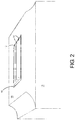
FIGS. 1 and2 are perspective views of portions of a prior art fluid ejection head; -
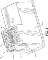
FIG. 3 is a perspective view of a fluid supply body having a pedestal chip mount surface according to an embodiment of the present disclosure; -
FIG. 4 is a cutaway view of a portion of the fluid supply body ofFIG. 3 illustrating the pedestal chip mount surface; -
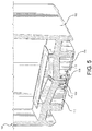
FIG. 5 is a cutaway view of a portion of the fluid supply body ofFIG. 3 illustrating a filter and a filter tower within a cartridge body for the ejection head. - Examples of prior art
thermoplastic bodies 10 for providing fluid to be ejected by a fluid ejection head attached to the body are illustrated inFIGS. 1 and2 . For simplification purposes only, the term "chip" is intended to include a semiconductor chip containing fluid ejectors thereon and a nozzle plate attached to the chip that collectively provides a fluid ejection head. Details of the fluid ejection head components are well known in the art and thus are not reproduced here. Of the components of the ejection head, thechip 12 is the most critical component. Thechip 12 may be made of semiconductor or ceramic materials and are fragile compared to thebody 10. Accordingly, care must be taken to assure that the chips are not damaged during assembly of the fluid ejection heads or during use. However, current designs provide inadequate protection for the chip and thus the chips are prone to damage. In the description that follows and appended claims, the term "damage" may refer to stress, including thermal stress or drop stress, shock, vibration, etc. that may adversely impact the performance of the chip of a fluid ejection head. - With reference to
FIG. 1 , the ejection head including thechip 12 is attached to thebody 10 in achip pocket 16 or recessed area in asurface 18 of thebody 10. Thechip 12 is relatively small and may have a length (L) of from about 10 to about 100 millimeters by from about 3 to about 10 millimeters in width (W) by from about 200 to about 800 microns in thickness (T). Thechip 12 includes one or morefluid feed slots 14, defined by etching through the thickness T of thechip 12, for supplying fluid from thebody 10 to ejection actuators on a device surface of thechip 12. InFIG. 1 , threeslots 14 in thechip 12 are illustrated, however, thechip 12 may have more or fewer of theslots 14. Thebody 10 may be made of a polymeric material, such as amorphous thermoplastic polyetherimide materials, glass filled thermoplastic polyethylene terephthalate resin materials, syndiotactic polystyrene containing glass fiber, polyphenylene ether/polystyrene alloy resin and polyamide/polyphenylene ether alloy resin. - The chip is typically surrounded on all sides by the
body 10 after being inserted into thechip pocket 16. For example, inFIGS. 1 and2 , thechip 12 is shown being placed into a standard rectangular pocket. Thechip pocket 16 includesslots 20 for supplying fluid from thebody 10 to theejection head chip 12 corresponding to theslots 14 in thechip 12. It is important that theslots 20 in thechip pocket 16 remain aligned with thefeed slots 14 formed in the chip in order to maximize performance of thechip 12. For that reason, a thermally curable adhesive is used to attach thechip 12 to thebody 10 in thechip pocket 16 to provide the assembled structure illustrated inFIG. 2 . The adhesive may be an epoxy adhesive. The thickness of adhesive in thechip pocket 16 may range from about 25 microns to about 250 microns. Heat is typically required to cure the adhesive and fixedly attach thechip 12 to thebody 10 in thechip pocket 16. - The
body 10 and thechip 12 often have different coefficients of thermal expansion (CTE). For example, thebody 10 may have a coefficient of thermal expansion (CTE) of about 42 microns/meter per °C. By contrast, thechip 12 may have a CTE of about 2 to about 3 microns/meter per °C. Additionally, the adhesive used may have a different CTE from thebody 10 or thechip 12. The different CTEs of the materials become important during a procedure for attaching thechip 12 to thebody 10. During this process there may be a cure cycle temperature change of approximately 60°C - 80°C, which the temperature change may cause thermal expansion of thechip 12, thebody 10, and the adhesive. Since thebody 10 has an order of magnitude higher thermal expansion coefficient than thechip 12, shrinkage in thebody 10 may be substantially greater than shrinkage of thechip 12 as thechip 12 and thebody 10 cool. Similarly, the shrinkage rate of the adhesive may vary widely from the shrinkage rate of thebody 10 orchip 12. Shrinkage of thebody 10 may cause damage in the form of stress or deformation to the chip, the nozzle plate, etc., as one component shrinks quickly or to a larger degree while other components shrink slowly or to a lesser degree. - For the reasons above, the
chip 12 is under some level of stress due simply to the manufacturing process. This inherent stress can add to the fragility of the chip. Since thechip 12 is already under stress, added stress or shock may damage to thechip 12, cause it to break or cause it to perform poorly. What is needed, therefore, is a method and apparatus for reducing the potential for damage to thechip 12 by reducing the amount of stress placed on the chip during the manufacturing process and by also reducing the amount of stress that is transmitted to the chip as a result of drops, sudden impacts, etc. - With reference now to
FIGS. 3-5 , there is provided afluid ejection head 100 designed for reducing chip damage according to an embodiment of the present disclosure. Thefluid ejection head 100 includes afluid supply body 102 having anosepiece 104 with at least onefluid supply port 106 formed therein. Apedestal 108 extends outwards from an exterior surface of thenosepiece 104 proximate the at least onefluid supply port 106. Thepedestal 108 has a perimeter edge and there is a semiconductorchip mounting surface 110 formed within that perimeter edge. A semiconductor chip may be mounted onto the mountingsurface 110 using the adhesive described above. In certain embodiments, the mountingsurface 110 is somewhat dog-bone shaped. This shape minimizes the amount of plastic material that the chip is attached to along the sides, while maintaining a wide pocket on the ends for corrosion protection. The narrow areas along the length of the chip allow the strength of the plastic to be less than the strength of the chip. It also reduces the likelihood of the adhesive climbing the sides of the chip, which has been shown to cause stresses in the chip, which in turn cause deflection in the nozzle plate. The ends being wider also allow for a larger pocket area to dispense the adhesive which can be forced into the back side of the flexible circuit as a corrosion inhibitor. - Additionally, a flexible
circuit bonding surface 112 extends outwards from an exterior surface of thenosepiece 104 adjacent the perimeter edge of thepedestal 108. In some embodiments, the flexiblecircuit bonding surface 112 is located only on opposing side surfaces of the pedestal. However, in other embodiments, the flexiblecircuit bonding surface 112 is located on opposing side surfaces of the pedestal as well as opposing end surfaces. Adamage reducing structure 115 is located between the perimeter edge of the pedestal and the flexible circuit bonding surface. Thedamage reducing structure 115 is intended to isolatepedestal 108 from the flexiblecircuit bonding surface 112. Thedamage reducing structure 115 also reduces damage caused to a semiconductor chip mounted on the pedestal by limiting shock forces, vibrations, and the like that are transmitted through thebody 102 to thechip mounting surface 110 and the chip that is mounted there. - In this particular case, the
damage reducing structure 115 is a void space or air space that separates the perimeter edge of thepedestal 108 from the flexiblecircuit bonding surface 112. By disassociating or isolating thepedestal 108 from the surrounding structure, forces traveling through the body as a result of a drop or impact, for example, are reduced or eliminated before they reach the chip mounted on the pedestal. The chip is less likely to be damaged by these forces. In the prior art structures shown inFIGS. 1-2 , shock waves and the like can easily travel from the body directly into the chip and the adhesive bond connecting the chip to the chip mounting surface. However, as shown best inFIG. 4 , shock waves flowing through thebody 102 cannot flow directly to thechip mounting surface 110 and, therefore, to the chip mounted on that surface. As a result of the isolation of thepedestal 108 from the surrounding structure, those shock waves have only one pathway to the chip. Shock waves must pass up through thepedestal 108 before reaching the chip mounted thereon. This indirect pathway greatly reduces damage to the chip and may even prevent damage to the chip entirely. - In other embodiments, the space between the perimeter edge of the
pedestal 108 and the flexiblecircuit bonding surface 112 may not be simply a void space. Instead, thedamage reducing structure 115 may be a compressible material that limits the transmission of shock forces from the flexiblecircuit bonding surface 112 to thepedestal 108. Although the space may be filled, it is still important to reduce the forces acting on the chip in order to avoid damage to the chip. For example, one material that may serve as a suitabledamage reducing structure 115 is a corrosion resistant compressible member such as a silicone rubber. - In addition to isolating the
pedestal 108 from the surrounding flexiblecircuit bonding surface 112, in certain embodiments, damage to the chip may be further reduced by replacing the normally solid or continuous flexible circuit bonding surface with a ribbed structure. As mentioned above, the chip is often surrounded on all sides by the body after being inserted into the chip pocket. In the past, the chip and the chip pocket were in substantially continuous contact with one another. This allowed shock forces to be very easily transmitted to the chip. Additionally, due to the differences in CTEs, the application of heat during the adhesive bonding process caused the body to expand and contract at a higher rate than the chip, which could damage the chip. - In the present device, however, the flexible
circuit bonding surface 112 that forms the pocket is made using a number ofribs 114. Theribs 114 provide a convenient location for mounting a flexible circuit. The shape of theribs 114, including a top surface of the ribs, may vary. However, it is preferable that at least a portion of the top surface of the ribs is planar to allow for the flexible circuit to be easily mounted thereon. - It is believed that this ribbed structure reduces the transmission of shock forces from the
body 102 to thechip mounting surface 110 and, consequently, to thechip 12 itself. Adamage reducing structure 115 may be located between each adjacent pair ofribs 114 to provide even more protection for thechip 12. For example, thedamage reducing structure 115 located between each adjacent pair of the plurality ofribs 114 may be a void space. With reference toFIGS. 1 and2 , in the past, the expansion of thebody 10 was constrained to expand in a single direction (i.e., into the chip pocket 16) due to the continuous nature of thesurface 18 surrounding the chip pocket. The expansion and contraction of thebody 10 had a tendency to damage to thechip 12 by placing thermal expansion stresses on thechip 12. However, as shown inFIG. 3-5 , since the amount of material forming the flexiblecircuit bonding surface 112 is reduced, it is believed that the strength of the expanded material is reduced. Reducing the strength of the plastic holding the chip allows the chip's strength to dominate and reduces the likelihood that the chip will be damaged whenever thebody 102 expands and contracts, such as during the bonding process. - Reducing the amount of material that forms the flexible
circuit bonding surface 112 has advantages, as discussed above, but reducing the amount of material too much may cause problems. For example, it is believed that eliminating too much material from the flexiblecircuit bonding surface 112 might cause it to be weakened such that it cannot provide adequate support for the flexible circuit during manufacturing or during use. Additionally, the flexiblecircuit bonding surface 112 provides some support to thepedestal 108. If thepedestal 108 were completely isolated and extended up from thenosepiece 104 without any surrounding structure, it is believed that the likelihood of damage to the chip would increase. For these reasons, some minimum amount of material surrounding thepedestal 108 is recommended. For example, in some embodiments, there are at least three ribs located adjacent each side surface of thepedestal 108 and at least two ribs located adjacent each end surface of the pedestal. However, more orfewer ribs 114 may be used. - In addition to changing the number of
ribs 114 present, varying the thickness Y, height and length X, and orientation of theribs 114 may allow for the amount of material to be varied, as desired while maintaining sufficient strength. As shown inFIG. 4 , the thickness Y of theribs 114 may vary and multiple thicknesses may be used to form the flexiblecircuit bonding surface 112. Similarly, the orientation of theribs 114 may vary. In certain embodiments, the angle θ between a first rib and a second rib may be greater than 0° and less than 180°. In other embodiments, θ is greater than 45° and less than 135°. In the embodiment shown inFIG. 4 , the ribs located along the opposing sides of thepedestal 108 are at approximately right angles to the ribs located along opposing ends of thepedestal 108, such that θ is approximately 90°. -
- 10 : body
- 12 : chip
- 14 : slot
- 16 : chip pocket
- 18 : surface
- 20 : slot
- 100 : fluid ejection head
- 102 : fluid supply body
- 104 : nosepiece
- 106 : fluid supply port
- 108 : pedestal
- 110 : mounting surface
- 112 : flexible circuit bonding surface
- 114 : ribs
- 115 : damage reducing structure
- T : thickness
- L : length
- W : width
- X : length
- Y : thickness
Claims (15)
- A fluid ejection head (100), characterized by comprising:a fluid supply body (102) configured to have a nosepiece (104) with at least one fluid supply port (106) formed therein;a pedestal (108) configured to extend outwards from an exterior surface of the nosepiece (104) proximate the at least one fluid supply port (106), the pedestal (108) having perimeter edge and having a semiconductor chip mounting surface (110) formed within the perimeter edge;a flexible circuit bonding surface (112) configured to extend outwards from the exterior surface adjacent the perimeter edge of the pedestal (108); anda damage reducing structure (115) configured to be located between the perimeter edge and the flexible circuit bonding surface (112).
- The fluid ejection head (100) of claim 1, characterized in that, the damage reducing structure (115) is a void space configured to separate the perimeter edge and the flexible circuit bonding surface (112).
- The fluid ejection head (100) of claim 1 or claim 2, characterized in that, the damage reducing structure (115) comprises a corrosion resistant compressible member.
- The fluid ejection head (100) of any one of claims 1-3, characterized in that, the pedestal (108) configured to have opposing side surfaces and opposing end surfaces and wherein the flexible circuit bonding surface (112) is disposed adjacent each of the side surfaces and the end surfaces of the pedestal (108).
- The fluid ejection head (100) of any one of claims 1-3, characterized in that, the flexible circuit bonding surface (112) comprises a plurality of ribs (114) and the damage reducing structure (115) located between each adjacent pair of the plurality of ribs (114).
- The fluid ejection head (100) of claim 5, characterized in that, the damage reducing structure (115) configured to be located between each adjacent pair of the plurality of ribs (114) is a void space.
- The fluid ejection head (100) of claim 5 or claim 6, characterized in that, the pedestal (108) configured to have opposing side surfaces and opposing end surfaces and wherein at least three ribs (114) are located adjacent each side surface and at least two ribs (114) are located adjacent each end surface of the pedestal (108).
- The fluid ejection head (100) of any one of claims 5-7, characterized in that, the plurality of ribs (114) comprises a substantially planar top surface configured to form the flexible circuit bonding surface (112).
- The fluid ejection head (100) of any one of claims 5-8, characterized in that, the plurality of ribs (114) comprises ribs (114) configured to have a first length and ribs (114) having a second length.
- The fluid ejection head (100) of any one of claims 5-9, characterized in that, the plurality of ribs (114) comprises a first rib and a second rib that is oriented at an angle 0 with respect to the first rib, wherein 0 is greater than 0° and less than 180°.
- The fluid ejection head (100) of any one of claims 1-9, characterized in that, the semiconductor chip mounting surface (110) is dog-bone shaped.
- A method for reducing damage to a semiconductor chip attached to a nosepiece (104) of a fluid supply body (102) having at least one fluid supply port (106), the method characterized by comprising the steps of:providing a pedestal (108) extending outwards from an exterior surface of the nosepiece (104), the pedestal (108) having perimeter edge and having a semiconductor chip mounting surface (110) formed within the perimeter edge;providing a flexible circuit bonding surface (112) extending outwards from the exterior surface adjacent the perimeter edge of the pedestal (108);providing a damage reducing structure (115) between the perimeter edge and the flexible circuit bonding surface (112) to reduce damage to a semiconductor chip attached to the pedestal (108); andadhesively attaching a semiconductor chip to the semiconductor chip mounting surface (110).
- The method of claim 12, characterized in that, the damage reducing structure (115) is a void space configured to separate the perimeter edge and the flexible circuit bonding surface (112).
- The method of claim 12, characterized in that, the pedestal (108) configured to have opposing side surfaces and opposing end surfaces and wherein the flexible circuit bonding surface (112) is disposed adjacent each of the side and end surfaces of the pedestal (108).
- The method of claim 12, characterized in that, the flexible circuit bonding surface (112) comprises a plurality of ribs (114) and the damage reducing structure (115) configured to be located between each adjacent pair of the plurality of ribs (114) is a void space.
Applications Claiming Priority (1)
| Application Number | Priority Date | Filing Date | Title |
|---|---|---|---|
| US15/371,632 US9987644B1 (en) | 2016-12-07 | 2016-12-07 | Pedestal chip mount for fluid delivery device |
Publications (2)
| Publication Number | Publication Date |
|---|---|
| EP3332967A1 true EP3332967A1 (en) | 2018-06-13 |
| EP3332967B1 EP3332967B1 (en) | 2021-01-13 |
Family
ID=60574470
Family Applications (1)
| Application Number | Title | Priority Date | Filing Date |
|---|---|---|---|
| EP17205316.7A Active EP3332967B1 (en) | 2016-12-07 | 2017-12-05 | Fluid ejection head and method for reducing damage to semiconductor chip attached to nosepiece of fluid supply body for a fluid ejection head |
Country Status (4)
| Country | Link |
|---|---|
| US (1) | US9987644B1 (en) |
| EP (1) | EP3332967B1 (en) |
| JP (1) | JP7047356B2 (en) |
| CN (1) | CN108162599B (en) |
Cited By (2)
| Publication number | Priority date | Publication date | Assignee | Title |
|---|---|---|---|---|
| WO2020222766A1 (en) * | 2019-04-29 | 2020-11-05 | Hewlett-Packard Development Company, L.P. | Fluidic dies with conductive members |
| EP4046808A1 (en) * | 2021-02-17 | 2022-08-24 | Funai Electric Co., Ltd. | Cartridge for jetting fluid |
Families Citing this family (2)
| Publication number | Priority date | Publication date | Assignee | Title |
|---|---|---|---|---|
| US11865843B2 (en) | 2021-11-09 | 2024-01-09 | Funai Electric Co., Ltd | Fluid cartridge with vented insert |
| US12583230B2 (en) | 2021-11-09 | 2026-03-24 | Brady Worldwide, Inc. | Fluid cartridge with vented insert |
Citations (9)
| Publication number | Priority date | Publication date | Assignee | Title |
|---|---|---|---|---|
| US5538586A (en) * | 1994-10-04 | 1996-07-23 | Hewlett-Packard Company | Adhesiveless encapsulation of tab circuit traces for ink-jet pen |
| US6244696B1 (en) * | 1999-04-30 | 2001-06-12 | Hewlett-Packard Company | Inkjet print cartridge design for decreasing ink shorts by using an elevated substrate support surface to increase adhesive sealing of the printhead from ink penetration |
| US6257703B1 (en) * | 1996-07-31 | 2001-07-10 | Canon Kabushiki Kaisha | Ink jet recording head |
| US20060012651A1 (en) * | 2004-07-16 | 2006-01-19 | Lee Young-Su | Inkjet cartridge |
| US20090066759A1 (en) * | 2007-09-12 | 2009-03-12 | Shirish Padmakar Mulay | Methods and apparatus for improved ejection head planarity and reduced ejection head damage |
| US20090309927A1 (en) * | 2008-06-17 | 2009-12-17 | Canon Kabushiki Kaisha | Inkjet printing head |
| US20120229572A1 (en) * | 2011-03-10 | 2012-09-13 | Canon Kabushiki Kaisha | Liquid ejection head |
| US20120274705A1 (en) * | 2011-04-29 | 2012-11-01 | Petersen Daniel W | Printhead assembly |
| US20160236468A1 (en) * | 2013-09-25 | 2016-08-18 | Hewlett-Packard Develoment Company, L.P. | Printhead assembly with one-piece printhead support |
Family Cites Families (11)
| Publication number | Priority date | Publication date | Assignee | Title |
|---|---|---|---|---|
| US5751324A (en) * | 1996-03-14 | 1998-05-12 | Lexmark International, Inc. | Ink jet cartridge body with vented die cavity |
| JP3492098B2 (en) * | 1996-07-31 | 2004-02-03 | キヤノン株式会社 | Inkjet recording head |
| US6227651B1 (en) * | 1998-09-25 | 2001-05-08 | Hewlett-Packard Company | Lead frame-mounted ink jet print head module |
| JP2002079655A (en) | 2000-09-06 | 2002-03-19 | Canon Inc | Ink jet recording head and ink jet recording apparatus |
| US7149090B2 (en) | 2001-09-11 | 2006-12-12 | Brother Kogyo Kabushiki Kaisha | Structure of flexible printed circuit board |
| KR100612261B1 (en) | 2004-12-10 | 2006-08-14 | 삼성전자주식회사 | Inkjet Cartridge and Manufacturing Method Thereof |
| JP4724484B2 (en) | 2005-07-08 | 2011-07-13 | キヤノン株式会社 | Recording head and ink jet recording apparatus |
| JP4325656B2 (en) * | 2006-09-29 | 2009-09-02 | ブラザー工業株式会社 | Inkjet printer |
| JP5541655B2 (en) | 2008-06-17 | 2014-07-09 | キヤノン株式会社 | Recording head |
| JPWO2012086520A1 (en) | 2010-12-22 | 2014-05-22 | コニカミノルタ株式会社 | Ink jet head unit and ink jet recording apparatus |
| JP5843720B2 (en) | 2012-07-25 | 2016-01-13 | キヤノン株式会社 | Inkjet recording head |
-
2016
- 2016-12-07 US US15/371,632 patent/US9987644B1/en active Active
-
2017
- 2017-12-04 CN CN201711258436.0A patent/CN108162599B/en active Active
- 2017-12-05 EP EP17205316.7A patent/EP3332967B1/en active Active
- 2017-12-05 JP JP2017233051A patent/JP7047356B2/en active Active
Patent Citations (9)
| Publication number | Priority date | Publication date | Assignee | Title |
|---|---|---|---|---|
| US5538586A (en) * | 1994-10-04 | 1996-07-23 | Hewlett-Packard Company | Adhesiveless encapsulation of tab circuit traces for ink-jet pen |
| US6257703B1 (en) * | 1996-07-31 | 2001-07-10 | Canon Kabushiki Kaisha | Ink jet recording head |
| US6244696B1 (en) * | 1999-04-30 | 2001-06-12 | Hewlett-Packard Company | Inkjet print cartridge design for decreasing ink shorts by using an elevated substrate support surface to increase adhesive sealing of the printhead from ink penetration |
| US20060012651A1 (en) * | 2004-07-16 | 2006-01-19 | Lee Young-Su | Inkjet cartridge |
| US20090066759A1 (en) * | 2007-09-12 | 2009-03-12 | Shirish Padmakar Mulay | Methods and apparatus for improved ejection head planarity and reduced ejection head damage |
| US20090309927A1 (en) * | 2008-06-17 | 2009-12-17 | Canon Kabushiki Kaisha | Inkjet printing head |
| US20120229572A1 (en) * | 2011-03-10 | 2012-09-13 | Canon Kabushiki Kaisha | Liquid ejection head |
| US20120274705A1 (en) * | 2011-04-29 | 2012-11-01 | Petersen Daniel W | Printhead assembly |
| US20160236468A1 (en) * | 2013-09-25 | 2016-08-18 | Hewlett-Packard Develoment Company, L.P. | Printhead assembly with one-piece printhead support |
Cited By (4)
| Publication number | Priority date | Publication date | Assignee | Title |
|---|---|---|---|---|
| WO2020222766A1 (en) * | 2019-04-29 | 2020-11-05 | Hewlett-Packard Development Company, L.P. | Fluidic dies with conductive members |
| CN113710494A (en) * | 2019-04-29 | 2021-11-26 | 惠普发展公司,有限责任合伙企业 | Fluid die with conductive member |
| US11279130B2 (en) | 2019-04-29 | 2022-03-22 | Hewlett-Packard Development Company, L.P. | Fluidic dies with conductive members |
| EP4046808A1 (en) * | 2021-02-17 | 2022-08-24 | Funai Electric Co., Ltd. | Cartridge for jetting fluid |
Also Published As
| Publication number | Publication date |
|---|---|
| JP2018094920A (en) | 2018-06-21 |
| JP7047356B2 (en) | 2022-04-05 |
| CN108162599B (en) | 2019-08-27 |
| US20180154385A1 (en) | 2018-06-07 |
| US9987644B1 (en) | 2018-06-05 |
| CN108162599A (en) | 2018-06-15 |
| EP3332967B1 (en) | 2021-01-13 |
Similar Documents
| Publication | Publication Date | Title |
|---|---|---|
| US10479076B2 (en) | Droplet deposition head and manifold components therefor | |
| EP3332967B1 (en) | Fluid ejection head and method for reducing damage to semiconductor chip attached to nosepiece of fluid supply body for a fluid ejection head | |
| US7712870B2 (en) | Ink jet recording head with sealant filling region in substrate | |
| EP3318408B1 (en) | Liquid discharge head and recording device using the same | |
| US6502926B2 (en) | Ink jet semiconductor chip structure | |
| US8388778B2 (en) | Print head with reduced bonding stress and method | |
| JP2015231731A (en) | Liquid discharge head, manufacturing method thereof, and liquid discharge apparatus | |
| US7819506B2 (en) | Flexible encapsulant materials for micro-fluid ejection heads and methods relating thereto | |
| US8827424B2 (en) | Liquid ejection head | |
| KR20090009919A (en) | Print head module | |
| JP5145636B2 (en) | Droplet discharge head and droplet discharge apparatus | |
| US20090066759A1 (en) | Methods and apparatus for improved ejection head planarity and reduced ejection head damage | |
| JP2001010048A5 (en) | ||
| CN100369748C (en) | Liquid ejection head, liquid ejection device, and method for manufacturing liquid ejection head | |
| JP2003039679A (en) | Inkjet recording head | |
| US7918536B2 (en) | Ink jet recording apparatus with adhesively bonded ink jet head chip | |
| US8240796B2 (en) | Fluid ejector housing insert | |
| US9844937B1 (en) | Method and apparatus for minimizing via compression in a fluid ejection head | |
| US8240817B2 (en) | Bonded housing and fluid ejector | |
| EP1070586B1 (en) | An acoustic ink jet printhead design and method of operation utilizing ink cross-flow | |
| JP2005119292A (en) | Droplet discharging head | |
| JP2007069475A (en) | Ink jet head and manufacturing method thereof | |
| KR20040099285A (en) | Ink jet head | |
| JP2025008201A (en) | Liquid ejection head and liquid ejection device | |
| JP2009034919A (en) | Method for manufacturing liquid droplet ejecting head |
Legal Events
| Date | Code | Title | Description |
|---|---|---|---|
| PUAI | Public reference made under article 153(3) epc to a published international application that has entered the european phase |
Free format text: ORIGINAL CODE: 0009012 |
|
| STAA | Information on the status of an ep patent application or granted ep patent |
Free format text: STATUS: THE APPLICATION HAS BEEN PUBLISHED |
|
| AK | Designated contracting states |
Kind code of ref document: A1 Designated state(s): AL AT BE BG CH CY CZ DE DK EE ES FI FR GB GR HR HU IE IS IT LI LT LU LV MC MK MT NL NO PL PT RO RS SE SI SK SM TR |
|
| AX | Request for extension of the european patent |
Extension state: BA ME |
|
| STAA | Information on the status of an ep patent application or granted ep patent |
Free format text: STATUS: REQUEST FOR EXAMINATION WAS MADE |
|
| 17P | Request for examination filed |
Effective date: 20181018 |
|
| RBV | Designated contracting states (corrected) |
Designated state(s): AL AT BE BG CH CY CZ DE DK EE ES FI FR GB GR HR HU IE IS IT LI LT LU LV MC MK MT NL NO PL PT RO RS SE SI SK SM TR |
|
| GRAP | Despatch of communication of intention to grant a patent |
Free format text: ORIGINAL CODE: EPIDOSNIGR1 |
|
| STAA | Information on the status of an ep patent application or granted ep patent |
Free format text: STATUS: GRANT OF PATENT IS INTENDED |
|
| INTG | Intention to grant announced |
Effective date: 20200916 |
|
| RIN1 | Information on inventor provided before grant (corrected) |
Inventor name: ANDERSON JR., JAMES D. |
|
| GRAS | Grant fee paid |
Free format text: ORIGINAL CODE: EPIDOSNIGR3 |
|
| GRAA | (expected) grant |
Free format text: ORIGINAL CODE: 0009210 |
|
| STAA | Information on the status of an ep patent application or granted ep patent |
Free format text: STATUS: THE PATENT HAS BEEN GRANTED |
|
| AK | Designated contracting states |
Kind code of ref document: B1 Designated state(s): AL AT BE BG CH CY CZ DE DK EE ES FI FR GB GR HR HU IE IS IT LI LT LU LV MC MK MT NL NO PL PT RO RS SE SI SK SM TR |
|
| REG | Reference to a national code |
Ref country code: GB Ref legal event code: FG4D |
|
| REG | Reference to a national code |
Ref country code: CH Ref legal event code: EP |
|
| REG | Reference to a national code |
Ref country code: IE Ref legal event code: FG4D |
|
| REG | Reference to a national code |
Ref country code: DE Ref legal event code: R096 Ref document number: 602017031311 Country of ref document: DE |
|
| REG | Reference to a national code |
Ref country code: AT Ref legal event code: REF Ref document number: 1354262 Country of ref document: AT Kind code of ref document: T Effective date: 20210215 |
|
| REG | Reference to a national code |
Ref country code: AT Ref legal event code: MK05 Ref document number: 1354262 Country of ref document: AT Kind code of ref document: T Effective date: 20210113 |
|
| REG | Reference to a national code |
Ref country code: NL Ref legal event code: MP Effective date: 20210113 |
|
| REG | Reference to a national code |
Ref country code: LT Ref legal event code: MG9D |
|
| PG25 | Lapsed in a contracting state [announced via postgrant information from national office to epo] |
Ref country code: LT Free format text: LAPSE BECAUSE OF FAILURE TO SUBMIT A TRANSLATION OF THE DESCRIPTION OR TO PAY THE FEE WITHIN THE PRESCRIBED TIME-LIMIT Effective date: 20210113 Ref country code: BG Free format text: LAPSE BECAUSE OF FAILURE TO SUBMIT A TRANSLATION OF THE DESCRIPTION OR TO PAY THE FEE WITHIN THE PRESCRIBED TIME-LIMIT Effective date: 20210413 Ref country code: FI Free format text: LAPSE BECAUSE OF FAILURE TO SUBMIT A TRANSLATION OF THE DESCRIPTION OR TO PAY THE FEE WITHIN THE PRESCRIBED TIME-LIMIT Effective date: 20210113 Ref country code: HR Free format text: LAPSE BECAUSE OF FAILURE TO SUBMIT A TRANSLATION OF THE DESCRIPTION OR TO PAY THE FEE WITHIN THE PRESCRIBED TIME-LIMIT Effective date: 20210113 Ref country code: GR Free format text: LAPSE BECAUSE OF FAILURE TO SUBMIT A TRANSLATION OF THE DESCRIPTION OR TO PAY THE FEE WITHIN THE PRESCRIBED TIME-LIMIT Effective date: 20210414 Ref country code: NO Free format text: LAPSE BECAUSE OF FAILURE TO SUBMIT A TRANSLATION OF THE DESCRIPTION OR TO PAY THE FEE WITHIN THE PRESCRIBED TIME-LIMIT Effective date: 20210413 Ref country code: PT Free format text: LAPSE BECAUSE OF FAILURE TO SUBMIT A TRANSLATION OF THE DESCRIPTION OR TO PAY THE FEE WITHIN THE PRESCRIBED TIME-LIMIT Effective date: 20210513 |
|
| PG25 | Lapsed in a contracting state [announced via postgrant information from national office to epo] |
Ref country code: SE Free format text: LAPSE BECAUSE OF FAILURE TO SUBMIT A TRANSLATION OF THE DESCRIPTION OR TO PAY THE FEE WITHIN THE PRESCRIBED TIME-LIMIT Effective date: 20210113 Ref country code: AT Free format text: LAPSE BECAUSE OF FAILURE TO SUBMIT A TRANSLATION OF THE DESCRIPTION OR TO PAY THE FEE WITHIN THE PRESCRIBED TIME-LIMIT Effective date: 20210113 Ref country code: PL Free format text: LAPSE BECAUSE OF FAILURE TO SUBMIT A TRANSLATION OF THE DESCRIPTION OR TO PAY THE FEE WITHIN THE PRESCRIBED TIME-LIMIT Effective date: 20210113 Ref country code: LV Free format text: LAPSE BECAUSE OF FAILURE TO SUBMIT A TRANSLATION OF THE DESCRIPTION OR TO PAY THE FEE WITHIN THE PRESCRIBED TIME-LIMIT Effective date: 20210113 Ref country code: RS Free format text: LAPSE BECAUSE OF FAILURE TO SUBMIT A TRANSLATION OF THE DESCRIPTION OR TO PAY THE FEE WITHIN THE PRESCRIBED TIME-LIMIT Effective date: 20210113 |
|
| PG25 | Lapsed in a contracting state [announced via postgrant information from national office to epo] |
Ref country code: IS Free format text: LAPSE BECAUSE OF FAILURE TO SUBMIT A TRANSLATION OF THE DESCRIPTION OR TO PAY THE FEE WITHIN THE PRESCRIBED TIME-LIMIT Effective date: 20210513 |
|
| REG | Reference to a national code |
Ref country code: DE Ref legal event code: R097 Ref document number: 602017031311 Country of ref document: DE |
|
| PG25 | Lapsed in a contracting state [announced via postgrant information from national office to epo] |
Ref country code: CZ Free format text: LAPSE BECAUSE OF FAILURE TO SUBMIT A TRANSLATION OF THE DESCRIPTION OR TO PAY THE FEE WITHIN THE PRESCRIBED TIME-LIMIT Effective date: 20210113 Ref country code: EE Free format text: LAPSE BECAUSE OF FAILURE TO SUBMIT A TRANSLATION OF THE DESCRIPTION OR TO PAY THE FEE WITHIN THE PRESCRIBED TIME-LIMIT Effective date: 20210113 Ref country code: SM Free format text: LAPSE BECAUSE OF FAILURE TO SUBMIT A TRANSLATION OF THE DESCRIPTION OR TO PAY THE FEE WITHIN THE PRESCRIBED TIME-LIMIT Effective date: 20210113 |
|
| PLBE | No opposition filed within time limit |
Free format text: ORIGINAL CODE: 0009261 |
|
| STAA | Information on the status of an ep patent application or granted ep patent |
Free format text: STATUS: NO OPPOSITION FILED WITHIN TIME LIMIT |
|
| PG25 | Lapsed in a contracting state [announced via postgrant information from national office to epo] |
Ref country code: DK Free format text: LAPSE BECAUSE OF FAILURE TO SUBMIT A TRANSLATION OF THE DESCRIPTION OR TO PAY THE FEE WITHIN THE PRESCRIBED TIME-LIMIT Effective date: 20210113 Ref country code: RO Free format text: LAPSE BECAUSE OF FAILURE TO SUBMIT A TRANSLATION OF THE DESCRIPTION OR TO PAY THE FEE WITHIN THE PRESCRIBED TIME-LIMIT Effective date: 20210113 Ref country code: SK Free format text: LAPSE BECAUSE OF FAILURE TO SUBMIT A TRANSLATION OF THE DESCRIPTION OR TO PAY THE FEE WITHIN THE PRESCRIBED TIME-LIMIT Effective date: 20210113 |
|
| 26N | No opposition filed |
Effective date: 20211014 |
|
| PG25 | Lapsed in a contracting state [announced via postgrant information from national office to epo] |
Ref country code: ES Free format text: LAPSE BECAUSE OF FAILURE TO SUBMIT A TRANSLATION OF THE DESCRIPTION OR TO PAY THE FEE WITHIN THE PRESCRIBED TIME-LIMIT Effective date: 20210113 Ref country code: AL Free format text: LAPSE BECAUSE OF FAILURE TO SUBMIT A TRANSLATION OF THE DESCRIPTION OR TO PAY THE FEE WITHIN THE PRESCRIBED TIME-LIMIT Effective date: 20210113 |
|
| PG25 | Lapsed in a contracting state [announced via postgrant information from national office to epo] |
Ref country code: SI Free format text: LAPSE BECAUSE OF FAILURE TO SUBMIT A TRANSLATION OF THE DESCRIPTION OR TO PAY THE FEE WITHIN THE PRESCRIBED TIME-LIMIT Effective date: 20210113 |
|
| PG25 | Lapsed in a contracting state [announced via postgrant information from national office to epo] |
Ref country code: IT Free format text: LAPSE BECAUSE OF FAILURE TO SUBMIT A TRANSLATION OF THE DESCRIPTION OR TO PAY THE FEE WITHIN THE PRESCRIBED TIME-LIMIT Effective date: 20210113 |
|
| PG25 | Lapsed in a contracting state [announced via postgrant information from national office to epo] |
Ref country code: IS Free format text: LAPSE BECAUSE OF FAILURE TO SUBMIT A TRANSLATION OF THE DESCRIPTION OR TO PAY THE FEE WITHIN THE PRESCRIBED TIME-LIMIT Effective date: 20210513 |
|
| PG25 | Lapsed in a contracting state [announced via postgrant information from national office to epo] |
Ref country code: MC Free format text: LAPSE BECAUSE OF FAILURE TO SUBMIT A TRANSLATION OF THE DESCRIPTION OR TO PAY THE FEE WITHIN THE PRESCRIBED TIME-LIMIT Effective date: 20210113 |
|
| REG | Reference to a national code |
Ref country code: CH Ref legal event code: PL |
|
| GBPC | Gb: european patent ceased through non-payment of renewal fee |
Effective date: 20211205 |
|
| REG | Reference to a national code |
Ref country code: BE Ref legal event code: MM Effective date: 20211231 |
|
| PG25 | Lapsed in a contracting state [announced via postgrant information from national office to epo] |
Ref country code: LU Free format text: LAPSE BECAUSE OF NON-PAYMENT OF DUE FEES Effective date: 20211205 Ref country code: IE Free format text: LAPSE BECAUSE OF NON-PAYMENT OF DUE FEES Effective date: 20211205 Ref country code: GB Free format text: LAPSE BECAUSE OF NON-PAYMENT OF DUE FEES Effective date: 20211205 |
|
| PG25 | Lapsed in a contracting state [announced via postgrant information from national office to epo] |
Ref country code: FR Free format text: LAPSE BECAUSE OF NON-PAYMENT OF DUE FEES Effective date: 20211231 Ref country code: BE Free format text: LAPSE BECAUSE OF NON-PAYMENT OF DUE FEES Effective date: 20211231 |
|
| PG25 | Lapsed in a contracting state [announced via postgrant information from national office to epo] |
Ref country code: LI Free format text: LAPSE BECAUSE OF NON-PAYMENT OF DUE FEES Effective date: 20211231 Ref country code: CH Free format text: LAPSE BECAUSE OF NON-PAYMENT OF DUE FEES Effective date: 20211231 |
|
| PG25 | Lapsed in a contracting state [announced via postgrant information from national office to epo] |
Ref country code: HU Free format text: LAPSE BECAUSE OF FAILURE TO SUBMIT A TRANSLATION OF THE DESCRIPTION OR TO PAY THE FEE WITHIN THE PRESCRIBED TIME-LIMIT; INVALID AB INITIO Effective date: 20171205 |
|
| PG25 | Lapsed in a contracting state [announced via postgrant information from national office to epo] |
Ref country code: NL Free format text: LAPSE BECAUSE OF NON-PAYMENT OF DUE FEES Effective date: 20210113 Ref country code: CY Free format text: LAPSE BECAUSE OF FAILURE TO SUBMIT A TRANSLATION OF THE DESCRIPTION OR TO PAY THE FEE WITHIN THE PRESCRIBED TIME-LIMIT Effective date: 20210113 |
|
| PG25 | Lapsed in a contracting state [announced via postgrant information from national office to epo] |
Ref country code: MK Free format text: LAPSE BECAUSE OF FAILURE TO SUBMIT A TRANSLATION OF THE DESCRIPTION OR TO PAY THE FEE WITHIN THE PRESCRIBED TIME-LIMIT Effective date: 20210113 |
|
| PG25 | Lapsed in a contracting state [announced via postgrant information from national office to epo] |
Ref country code: TR Free format text: LAPSE BECAUSE OF FAILURE TO SUBMIT A TRANSLATION OF THE DESCRIPTION OR TO PAY THE FEE WITHIN THE PRESCRIBED TIME-LIMIT Effective date: 20210113 |
|
| PG25 | Lapsed in a contracting state [announced via postgrant information from national office to epo] |
Ref country code: MT Free format text: LAPSE BECAUSE OF FAILURE TO SUBMIT A TRANSLATION OF THE DESCRIPTION OR TO PAY THE FEE WITHIN THE PRESCRIBED TIME-LIMIT Effective date: 20210113 |
|
| REG | Reference to a national code |
Ref country code: DE Ref legal event code: R081 Ref document number: 602017031311 Country of ref document: DE Owner name: BRADY WORLDWIDE, INC., MILWAUKEE, US Free format text: FORMER OWNER: FUNAI ELECTRIC CO., LTD., DAITO, OSAKA, JP Ref country code: DE Ref legal event code: R082 Ref document number: 602017031311 Country of ref document: DE Representative=s name: BOULT WADE TENNANT LLP, DE |
|
| PGFP | Annual fee paid to national office [announced via postgrant information from national office to epo] |
Ref country code: DE Payment date: 20251229 Year of fee payment: 9 |