EP3331332A1 - Method of manufacturing substrate and substrate - Google Patents
Method of manufacturing substrate and substrate Download PDFInfo
- Publication number
- EP3331332A1 EP3331332A1 EP17201822.8A EP17201822A EP3331332A1 EP 3331332 A1 EP3331332 A1 EP 3331332A1 EP 17201822 A EP17201822 A EP 17201822A EP 3331332 A1 EP3331332 A1 EP 3331332A1
- Authority
- EP
- European Patent Office
- Prior art keywords
- conductive layer
- hole
- substrate according
- pth
- manufacturing
- Prior art date
- Legal status (The legal status is an assumption and is not a legal conclusion. Google has not performed a legal analysis and makes no representation as to the accuracy of the status listed.)
- Granted
Links
Images





Classifications
-
- H—ELECTRICITY
- H05—ELECTRIC TECHNIQUES NOT OTHERWISE PROVIDED FOR
- H05K—PRINTED CIRCUITS; CASINGS OR CONSTRUCTIONAL DETAILS OF ELECTRIC APPARATUS; MANUFACTURE OF ASSEMBLAGES OF ELECTRICAL COMPONENTS
- H05K1/00—Printed circuits
- H05K1/02—Details
- H05K1/11—Printed elements for providing electric connections to or between printed circuits
- H05K1/115—Via connections; Lands around holes or via connections
-
- H—ELECTRICITY
- H05—ELECTRIC TECHNIQUES NOT OTHERWISE PROVIDED FOR
- H05K—PRINTED CIRCUITS; CASINGS OR CONSTRUCTIONAL DETAILS OF ELECTRIC APPARATUS; MANUFACTURE OF ASSEMBLAGES OF ELECTRICAL COMPONENTS
- H05K3/00—Apparatus or processes for manufacturing printed circuits
- H05K3/0011—Working of insulating substrates or insulating layers
- H05K3/0044—Mechanical working of the substrate, e.g. drilling or punching
- H05K3/0047—Drilling of holes
-
- H—ELECTRICITY
- H05—ELECTRIC TECHNIQUES NOT OTHERWISE PROVIDED FOR
- H05K—PRINTED CIRCUITS; CASINGS OR CONSTRUCTIONAL DETAILS OF ELECTRIC APPARATUS; MANUFACTURE OF ASSEMBLAGES OF ELECTRICAL COMPONENTS
- H05K3/00—Apparatus or processes for manufacturing printed circuits
- H05K3/40—Forming printed elements for providing electric connections to or between printed circuits
- H05K3/4038—Through-connections; Vertical interconnect access [VIA] connections
- H05K3/4046—Through-connections; Vertical interconnect access [VIA] connections using auxiliary conductive elements, e.g. metallic spheres, eyelets, pieces of wire
-
- H—ELECTRICITY
- H05—ELECTRIC TECHNIQUES NOT OTHERWISE PROVIDED FOR
- H05K—PRINTED CIRCUITS; CASINGS OR CONSTRUCTIONAL DETAILS OF ELECTRIC APPARATUS; MANUFACTURE OF ASSEMBLAGES OF ELECTRICAL COMPONENTS
- H05K3/00—Apparatus or processes for manufacturing printed circuits
- H05K3/40—Forming printed elements for providing electric connections to or between printed circuits
- H05K3/4038—Through-connections; Vertical interconnect access [VIA] connections
- H05K3/4084—Through-connections; Vertical interconnect access [VIA] connections by deforming at least one of the conductive layers
-
- H—ELECTRICITY
- H05—ELECTRIC TECHNIQUES NOT OTHERWISE PROVIDED FOR
- H05K—PRINTED CIRCUITS; CASINGS OR CONSTRUCTIONAL DETAILS OF ELECTRIC APPARATUS; MANUFACTURE OF ASSEMBLAGES OF ELECTRICAL COMPONENTS
- H05K3/00—Apparatus or processes for manufacturing printed circuits
- H05K3/40—Forming printed elements for providing electric connections to or between printed circuits
- H05K3/42—Plated through-holes or plated via connections
-
- H—ELECTRICITY
- H05—ELECTRIC TECHNIQUES NOT OTHERWISE PROVIDED FOR
- H05K—PRINTED CIRCUITS; CASINGS OR CONSTRUCTIONAL DETAILS OF ELECTRIC APPARATUS; MANUFACTURE OF ASSEMBLAGES OF ELECTRICAL COMPONENTS
- H05K2201/00—Indexing scheme relating to printed circuits covered by H05K1/00
- H05K2201/10—Details of components or other objects attached to or integrated in a printed circuit board
- H05K2201/10227—Other objects, e.g. metallic pieces
- H05K2201/10242—Metallic cylinders
-
- H—ELECTRICITY
- H05—ELECTRIC TECHNIQUES NOT OTHERWISE PROVIDED FOR
- H05K—PRINTED CIRCUITS; CASINGS OR CONSTRUCTIONAL DETAILS OF ELECTRIC APPARATUS; MANUFACTURE OF ASSEMBLAGES OF ELECTRICAL COMPONENTS
- H05K2201/00—Indexing scheme relating to printed circuits covered by H05K1/00
- H05K2201/10—Details of components or other objects attached to or integrated in a printed circuit board
- H05K2201/10227—Other objects, e.g. metallic pieces
- H05K2201/10295—Metallic connector elements partly mounted in a hole of the PCB
- H05K2201/10303—Pin-in-hole mounted pins
-
- H—ELECTRICITY
- H05—ELECTRIC TECHNIQUES NOT OTHERWISE PROVIDED FOR
- H05K—PRINTED CIRCUITS; CASINGS OR CONSTRUCTIONAL DETAILS OF ELECTRIC APPARATUS; MANUFACTURE OF ASSEMBLAGES OF ELECTRICAL COMPONENTS
- H05K2201/00—Indexing scheme relating to printed circuits covered by H05K1/00
- H05K2201/10—Details of components or other objects attached to or integrated in a printed circuit board
- H05K2201/10227—Other objects, e.g. metallic pieces
- H05K2201/10401—Eyelets, i.e. rings inserted into a hole through a circuit board
-
- H—ELECTRICITY
- H05—ELECTRIC TECHNIQUES NOT OTHERWISE PROVIDED FOR
- H05K—PRINTED CIRCUITS; CASINGS OR CONSTRUCTIONAL DETAILS OF ELECTRIC APPARATUS; MANUFACTURE OF ASSEMBLAGES OF ELECTRICAL COMPONENTS
- H05K2201/00—Indexing scheme relating to printed circuits covered by H05K1/00
- H05K2201/10—Details of components or other objects attached to or integrated in a printed circuit board
- H05K2201/10227—Other objects, e.g. metallic pieces
- H05K2201/10409—Screws
-
- H—ELECTRICITY
- H05—ELECTRIC TECHNIQUES NOT OTHERWISE PROVIDED FOR
- H05K—PRINTED CIRCUITS; CASINGS OR CONSTRUCTIONAL DETAILS OF ELECTRIC APPARATUS; MANUFACTURE OF ASSEMBLAGES OF ELECTRICAL COMPONENTS
- H05K2203/00—Indexing scheme relating to apparatus or processes for manufacturing printed circuits covered by H05K3/00
- H05K2203/02—Details related to mechanical or acoustic processing, e.g. drilling, punching, cutting, using ultrasound
- H05K2203/0278—Flat pressure, e.g. for connecting terminals with anisotropic conductive adhesive
-
- H—ELECTRICITY
- H05—ELECTRIC TECHNIQUES NOT OTHERWISE PROVIDED FOR
- H05K—PRINTED CIRCUITS; CASINGS OR CONSTRUCTIONAL DETAILS OF ELECTRIC APPARATUS; MANUFACTURE OF ASSEMBLAGES OF ELECTRICAL COMPONENTS
- H05K3/00—Apparatus or processes for manufacturing printed circuits
- H05K3/30—Assembling printed circuits with electric components, e.g. with resistors
- H05K3/306—Assembling printed circuits with electric components, e.g. with resistors with lead-in-hole components
Definitions
- the embodiments discussed herein are directed to a method of manufacturing a substrate and a substrate.
- a so-called thick copper substrate has attracted attention as a printed-circuit board corresponding to large current.
- a base is formed by stacking a plurality of copper layers having a thickness of, for example, 70 ⁇ m or more via insulating resin layers (for example, glass epoxy resin layers).
- the base is formed with a plurality of through holes, and a copper plating layer connected to the copper layers is formed on an inner wall surface of the through hole.
- a terminal is inserted and bonded by solder filled in the through hole.
- a method of fixing the terminal in the through hole of the printed-circuit board without adhering it using solder for example, a method using a press-fit pin as the terminal is devised.
- the press-fit pin is inserted into and fixed to the through hole without requiring solder bonding.
- the press-fit pin is brought into contact with and fix to, by its mechanical resilient restoring force, a copper plating layer in the through hole into which the press-fit pin is inserted.
- Another problem is that, in the case of using the terminal such as the press-fit pin or the like in the thick copper substrate, if the copper plating layer on the inner wall surface of the through hole is thin, cracks occur due to thermal stress in the copper plating layer, caused by a difference in coefficient of thermal expansion between the copper layer and the resin layer.
- the plating method is low in accuracy of controlling the thickness of the copper plating layer and therefore has a difficulty in obtaining a hole diameter with a desired accuracy corresponding to the terminal such as the press-fit pin or the like.
- the copper plating layer is formed from the inner wall side surface of the through hole of the thick copper substrate to parts of the front and rear surfaces of the base, so that when the copper plating layer is formed thick, the front and rear surface parts become also thick. Therefore, the patterning property of the copper plating layer decreases, resulting in difficulty in microfabrication.
- the thickness of the copper plating layer is proportional to the plating treatment time, forming the copper plating layer thick leads to a significant decrease in productivity.
- a method of manufacturing a substrate includes: forming a first hole, the first hole penetrating a base; forming a conductive layer, the conductive layer covering an inner wall side surface of the first hole; inserting a columnar electric conductor into the first hole formed with the conductive layer; applying pressure in a vertical direction to the columnar electric conductor; and forming a second hole in the columnar electric conductor.
- a substrate in one aspect, includes: a base including a first hole being a through hole; a first conductive layer covering an inner wall side surface of the first hole; and a second conductive layer covering a side surface of the first conductive layer and including a second hole, wherein the second conductive layer is different in crystalline structure from the first conductive layer and has a Vickers hardness of a value of 30 Hv or more.
- a thick copper substrate is disclosed as a printed-circuit board and its configuration will be explained together with a manufacturing method thereof.
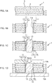
- Figs. 1A to 1D and Figs. 2A to 2C are schematic sectional views illustrating the method of manufacturing the thick copper substrate according to this embodiment in order of steps.
- a base 1 of the thick copper substrate is prepared.
- the base 1 is formed of, for example, a plurality of copper layers 2 having a predetermined thickness of 70 ⁇ m or more stacked via insulating resin layers (for example, glass epoxy resin layers) 3.
- a PTH (Plated Through Hole) 11 is formed in the base 1.
- a first through hole 11a is formed as a first hole in the base 1.
- a Cu layer is formed on the front surface and the rear surface of the base 1 including an inner wall side surface of the first through hole 11a by the plating method.
- the Cu layer is formed into a thickness of a value in a range of about 40 ⁇ m or more and 70 ⁇ m or less, for example, about 70 ⁇ m.
- patterning is performed on the front surface and the rear surface of the base 1 to remove a part of the Cu layer to thereby form a first conductive layer 11b extending from the inner wall side surface of the first through hole 11a up to parts on the front surface and on the rear surface of the base 1.
- the first conductive layer 11b a stacked structure of Cu/Ni/Au (Cu is at the lowermost layer) in place of forming the CU layer.
- the PTH 11 including the first conductive layer 11b covering the inner wall side surface of the first through hole 11a is formed.
- a Cu coin 12 is inserted into the PTH 11.
- the Cu coin 12 being a columnar Cu material is used as a columnar electric conductor to be inserted into the PTH 11.
- the Cu coin 12 is formed to have a length slightly larger than the thickness of the base 1, a cross-sectional shape in the same shape (circular shape here) as that of the first through hole 11a, and a diameter slightly smaller than the diameter of the PTH 11 (diameter of the first through hole 11a via the first conductive layer 11b).
- the Cu coin 12 has a Vickers hardness of a value in a range of 30 Hv or more and 400 Hv or less, here, about 100 Hv.
- the base 1 with the Cu coin 12 inserted into the PTH 11 is mounted and fixed onto a support table 10a.
- a pressing plate 10b is placed on the upper surface of the base 1, and applies pressure downward.
- the Cu coin 12 is reduced in length and expanded in diameter and thereby pressure-bonded to the first conductive layer 11b.
- Figs. 3A and 3B are photographs indicating a pressure bonding state between the Cu layer formed by the plating method and the Cu coin, and Fig. 3B indicates an enlarged appearance in a rectangular frame in Fig. 3A .
- Both of the first conductive layer 11b and the Cu coin 12 are made of the same Cu as a material in this embodiment, but the Cu material of the Cu coin 12 changes in quality due to the application of the pressure. As a result, the Cu coin 12 becomes different in crystalline state from the first conductive layer 11b formed by the plating method, and its crystal grains become larger than those of the first conductive layer 11b. Since the Cu coin 12 is pressure-bonded to the first conductive layer 11b, the first conductive layer 11b and the Cu coin 12 are brought into a close contact state without any gap therebetween on the inner wall side surface of the PTH 11.
- a second through hole 12a is formed as a second hole in the Cu coin 12.
- the thick copper substrate according to this embodiment is formed.
- the second through hole 12a is formed using a drill 20 at a central portion of the Cu coin 12.
- the drilling work is high in working accuracy and provides a pore diameter tolerance of about ⁇ 30 ⁇ m or less.
- the second through hole 12a is formed into, for example, a desired diameter of about 1.0 mm ⁇ 30 ⁇ m.
- a second conductive layer 12b composed of Cu covering the side surface (inner wall side surface of the PTH 11) of the first conductive layer 11b is formed as illustrated in Fig. 2B .
- the second conductive layer 12b is formed into a thickness of, for example, about 400 ⁇ m and is brought into close contact with and fixed to the side surface of the first conductive layer 11b.
- a press-fit pin 13 as a terminal is inserted into and fixed to the second through hole 12a.
- the press-fit pin 13 is made to be attachable to and detachable from the second through hole 12a, and is brought into contact with and fix to, by its mechanical resilient restoring force, the side surface of the second conductive layer 12b inside the second through hole 12a in which the press-fit pin 13 is inserted.
- the second conductive layer 12b in close contact with the side surface of the first conductive layer 11b in the PTH 11 is formed without the first conductive layer 11b being formed thick, thereby securing the conductive layer thickness on the inner wall side surface of the PTH 11.
- the second conductive layer 12b protects the first conductive layer 11b to suppress occurrence of cracks in the first conductive layer 11b. Since the first conductive layer 11b made by the plating method is formed thin, the first conductive layer 11b can be easily formed into a fine pattern without deteriorating the productivity of plating.
- the second conductive layer 12b being a conductive layer with which the press-fit pin 13 comes into contact has a Vickers hardness set to a value in a range of 30 Hv or more and 400 Hv or less.
- the conductive layer is required to have hardness to withstand a load in inserting the press-fit pin 13 (at a level of maintaining desired connection reliability even when receiving pressure contact from the press-fit pin 13).
- the lower limit value of the hardness is evaluated to be about 30 Hv in Vickers hardness.
- the conductive layer is too hard, appropriate press fitting of the Cu coin 12 into the PTH 11 becomes difficult at the step in Fig. 1D .
- the upper limit value of the hardness is evaluated to be about 400 Hv in Vickers hardness.
- Cu being a conductive material having a Vickers hardness of a value in a range of 30 Hv or more and 400 Hv or less is used as the material of the second conductive layer 12b.
- the second conductive layer 12b is surely brought into close contact with and fixed to the first conductive layer 11b to suppress occurrence of cracks in the first conductive layer 11b and realize a thick copper substrate securing the connection reliability even if the press-fit pin 13 is inserted thereinto and fixed thereto.
- the second conductive layer 12b covering the side surface of the first conductive layer 11b is formed to increase the conductive layer thickness on the inner wall side surface of the PTH 11, thereby increasing also the amount of current allowed to flow through one PTH 11. This makes it possible to reduce the number of PTHs 11 required for desired current to flow, thereby improving the degree of freedom in substrate design.
- the second conductive layer 12b with a desired thickness is accurately secured on the inner wall side surface of the PTH 11 without using solder. This realizes a thick copper substrate in which the press-fit pin 13 can be inserted into and fixed to the second through hole 12a with high connection reliability without damaging the first conductive layer 11b.
- a thick copper substrate is disclosed as in the first embodiment, but is different from the first embodiment in that the second hole formed in the Cu coin is different.
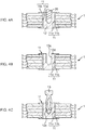
- Figs. 4A to 4C are schematic sectional views illustrating main steps of a method of manufacturing the thick copper substrate according to the modified example 1 of the first embodiment. Note that the same components as those of the thick copper substrate according to the first embodiment are denoted by the same numerals, and detailed explanation thereof will be omitted.
- the Cu coin 12 is pressure-bonded to the first conductive layer 11b.
- a non-through hole 12c not penetrating the Cu coin 12 is formed as a second hole in the Cu coin 12.
- the thick copper substrate according to this embodiment is formed.
- the non-through hole 12c is formed by working a central portion of the Cu coin 12 using the drill 20 down to a middle in the length direction of the Cu coin 12, for example, about half in the length direction.
- the drilling work is high in working accuracy and provides a pore diameter tolerance of about ⁇ 30 ⁇ m or less.
- the non-through hole 12c is formed into, for example, a desired diameter of about 1.0 mm ⁇ 30 ⁇ m.
- a second conductive layer 12d composed of Cu having a bottom portion and covering the side surface (inner wall side surface of the PTH 11) of the first conductive layer 11b is formed as illustrated in Fig. 4B .
- the second conductive layer 12d has a side surface portion formed into a thickness of, for example, about 400 ⁇ m and is brought into close contact with and fixed to the side surface of the first conductive layer 11b.
- the press-fit pin 13 is made to be attachable to and detachable from the non-through hole 12c, and is brought into contact with and fix to, by its mechanical resilient restoring force, the side surface of the second conductive layer 12d inside the non-through hole 12c in which the press-fit pin 13 is inserted.
- the second conductive layer 12d in close contact with the side surface of the first conductive layer 11b in the PTH 11 is formed without the first conductive layer 11b being formed thick, thereby securing the conductive layer thickness on the inner wall side surface of the PTH 11.
- the second conductive layer 12d protects the first conductive layer 11b to suppress occurrence of cracks in the first conductive layer 11b. Since the first conductive layer 11b made by the plating method is formed thin, the first conductive layer 11b can be easily formed into a fine pattern without deteriorating the productivity of plating.
- the conductive layer with which the press-fit pin 13 comes into contact here, the second conductive layer 12d has a Vickers hardness set to a value in a range of 30 Hv or more and 400 Hv or less.
- the conductive layer is required to have hardness to withstand a load in inserting the press-fit pin 13 (at a level of maintaining desired connection reliability even when receiving pressure contact from the press-fit pin 13).
- the lower limit value of the hardness is evaluated to be about 30 Hv in Vickers hardness.
- the conductive layer is too hard, appropriate press fitting of the Cu coin 12 into the PTH 11 becomes difficult at the step in Fig. 4B .
- the upper limit value of the hardness is evaluated to be about 400 Hv in Vickers hardness.
- Cu being a conductive material having a Vickers hardness of a value in a range of 30 Hv or more and 400 Hv or less is used as the material of the second conductive layer 12d.
- the second conductive layer 12d is surely brought into close contact with and fixed to the first conductive layer 11b to suppress occurrence of cracks in the first conductive layer 11b and realize a thick copper substrate securing the connection reliability even if the press-fit pin 13 is inserted thereinto and fixed thereto.
- the second conductive layer 12d covering the side surface of the first conductive layer 11b is formed to increase the conductive layer thickness on the inner wall side surface of the PTH 11, thereby increasing also the amount of current allowed to flow through one PTH 11. This makes it possible to reduce the number of PTHs 11 required for desired current to flow, thereby improving the degree of freedom in substrate design.
- the conductive layer (the second conductive layer 12d) with a desired thickness is accurately secured on the inner wall side surface of the PTH 11 without using solder. This realizes a thick copper substrate in which the press-fit pin 13 can be inserted into and fixed to the non-through hole 12c with high connection reliability without damaging the first conductive layer 11b.
- a thick copper substrate is disclosed as in the first embodiment, but is different from the first embodiment in that the conductive layer formed in the PTH is different.
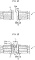
- Figs. 5A to 5C and Figs. 6A and 6B are schematic sectional views illustrating main steps of a method of manufacturing the thick copper substrate according to the modified example 2 of the first embodiment. Note that the same components as those of the thick copper substrate according to the first embodiment are denoted by the same numerals, and detailed explanation thereof will be omitted.
- the base 1 is formed with the PTH 11.
- a conductive material differing from Cu of the first conductive layer 11b here, an Al alloy is employed and the Al alloy coin 21 being a columnar Al alloy material is used as the columnar electric conductor to be inserted into the PTH 11.
- the Al alloy coin 21 is formed to have a length slightly larger than the thickness of the base 1, a cross-sectional shape in the same shape (circular shape here) as that of the first through hole 11a, and a diameter slightly smaller than the diameter of the PTH 11 (diameter of the first through hole 11a via the first conductive layer 11b).
- the Al alloy coin 21 has a Vickers hardness of a value in a range of 30 Hv or more and 400 Hv or less, here, about 150 Hv.
- one kind selected from Al, Fe, a Cu alloy, a Ni alloy, a Fe alloy and the like other than the Al alloy may be employed as the conductive material of the columnar electric conductor, and a coin made of the conductive material may be used in this modified example.
- the base 1 with the Al alloy coin 21 inserted into the PTH 11 is mounted and fixed onto the support table 10a.
- the pressing plate 10b is placed on the upper surface of the base 1, and applies pressure downward.
- the Al alloy coin 21 is reduced in length and expanded in diameter and thereby pressure-bonded to the first conductive layer 11b.
- the pressure-bonded Al alloy coin 21 is different in crystalline state from the first conductive layer 11b formed by the plating method. Since the Al alloy coin 21 is pressure-bonded to the first conductive layer 11b, the first conductive layer 11b and the Al alloy coin 21 are brought into a close contact state without any gap therebetween on the inner wall side surface of the PTH 11. Further, since a pressure-bonding form of applying pressure to the Al alloy coin 21 inserted into the PTH 11 is taken, a dent is generated in the Al alloy coin 21 at an edge portion at the uppermost portion of the PTH 11. This dent can be confirmed also by observing the base 1 from above.
- a second through hole 21a is formed in the Al alloy coin 21.
- the thick copper substrate according to this modified example is formed.
- the second through hole 21a is formed using the drill 20 at a central portion of the Al alloy coin 21.
- the drilling work is high in working accuracy and provides a pore diameter tolerance of about ⁇ 30 ⁇ m or less.
- the second through hole 21a is formed into, for example, a desired diameter of about 1.0 mm ⁇ 30 ⁇ m.
- a second conductive layer 21b composed of an Al alloy covering the side surface (inner wall side surface of the PTH 11) of the first conductive layer 11b is formed as illustrated in Fig. 6A .
- the second conductive layer 21b is formed into a thickness of, for example, about 400 ⁇ m and is brought into close contact with and fixed to the side surface of the first conductive layer 11b.
- the press-fit pin 13 is made to be attachable to and detachable from the second through hole 21a, and is brought into contact with and fix to, by its mechanical resilient restoring force, the side surface of the second conductive layer 21b inside the second through hole 21a in which the press-fit pin 13 is inserted.
- the second conductive layer 21b in close contact with the side surface of the first conductive layer 11b in the PTH 11 is formed without the first conductive layer 11b being formed thick, thereby securing the conductive layer thickness on the inner wall side surface of the PTH 11.
- the second conductive layer 21b protects the first conductive layer 11b to suppress occurrence of cracks in the first conductive layer 11b. Since the first conductive layer 11b made by the plating method is formed thin, the first conductive layer 11b can be easily formed into a fine pattern without deteriorating the productivity of plating.
- the conductive layer with which the press-fit pin 13 comes into contact here, the second conductive layer 21b has a Vickers hardness set to a value in a range of 30 Hv or more and 400 Hv or less.
- the conductive layer is required to have hardness to withstand a load in inserting the press-fit pin 13 (at a level of maintaining desired connection reliability even when receiving pressure contact from the press-fit pin 13).
- the lower limit value of the hardness is evaluated to be about 30 Hv in Vickers hardness.
- the conductive layer is too hard, appropriate press fitting of the Al alloy coin 21 into the PTH 11 becomes difficult at the step in Fig. 5B .
- the upper limit value of this hardness is evaluated to be about 400 Hv in Vickers hardness.
- an Al alloy being a conductive material having a Vickers hardness of a value in a range of 30 Hv or more and 400 Hv or less is used as the material of the second conductive layer 21b.
- the second conductive layer 21b is surely brought into close contact with and fixed to the first conductive layer 11b to suppress occurrence of cracks in the first conductive layer 11b and realize a thick copper substrate securing the connection reliability even if the press-fit pin 13 is inserted thereinto and fixed thereto.
- the second conductive layer 21b covering the side surface of the first conductive layer 11b is formed to increase the conductive layer thickness on the inner wall side surface of the PTH 11, thereby increasing also the amount of current allowed to flow through one PTH 11. This makes it possible to reduce the number of PTHs 11 required for desired current to flow, thereby improving the degree of freedom in substrate design.
- the conductive layer (the second conductive layer 21b) with a desired thickness is accurately secured on the inner wall side surface of the PTH 11 without using solder. This realizes a thick copper substrate in which the press-fit pin 13 can be inserted into and fixed to the second through hole 21a with high connection reliability without damaging the first conductive layer 11b.
- a thick copper substrate is disclosed as in the first embodiment, but is different from the first embodiment in that a terminal inserted into and fixed to a PTH is different.
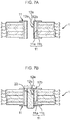
- Figs. 7A and 7B are schematic sectional views illustrating main steps of a method of manufacturing the thick copper substrate according to this embodiment. Note that the same components as those of the thick copper substrate according to the first embodiment are denoted by the same numerals, and detailed explanation thereof will be omitted.
- a second conductive layer 12b including a second through hole 12a is formed in a base 1 to cover an inner wall side surface of a first conductive layer 11b of the PTH 11.
- a thread groove 12e is formed on an inner wall side surface of the second through hole 12a.
- the thick copper substrate according to this embodiment is formed.
- the thread groove 12e being a female thread is formed on the inner wall side surface (side surface of the second conductive layer 12b) of the second through hole 12a by shaving the second through hole 12a. In this event, it is also possible to repair the thread groove by helical insert processing.
- a screw 22 as a terminal is engaged and fixed to the inside of the second through hole 12a as illustrated in Fig. 7B .
- the screw 22 is inserted into and fixed to the second through hole 12a having the inner wall side surface formed with the thread groove 12e.
- the screw 22 may be used also as a fixing member of the thick copper substrate with another not-illustrated printed-circuit board or the like to connect with the printed-circuit board or the like.
- the second conductive layer 12b in close contact with the side surface of the first conductive layer 11b in the PTH 11 is formed without the first conductive layer 11b being formed thick, thereby securing the conductive layer thickness on the inner wall side surface of the PTH 11.
- the second conductive layer 12b protects the first conductive layer 11b to suppress occurrence of cracks in the first conductive layer 11b. Since the first conductive layer 11b made by the plating method is formed thin, the first conductive layer 11b can be easily formed into a fine pattern without deteriorating the productivity of plating.
- a conductive layer to which the screw 22 is engaged and fixed here, the second conductive layer 12b has a Vickers hardness set to a value in a range of 30 Hv or more and 400 Hv or less.
- the conductive layer is required to have hardness to withstand the processing of forming the thread groove 12e.
- the lower limit value of the hardness is evaluated to be about 30 Hv in Vickers hardness.
- the upper limit value of the hardness is evaluated to be about 400 Hv in Vickers hardness.
- Cu being a conductive material having a Vickers hardness of a value in a range of 30 Hv or more and 400 Hv or less is used as the material of the second conductive layer 12b.
- the second conductive layer 12b is surely brought into close contact with and fixed to the first conductive layer 11b to suppress occurrence of cracks in the first conductive layer 11b and realize a thick copper substrate securing the connection reliability even if the thread groove 12e is formed therein.
- the second conductive layer 12b covering the side surface of the first conductive layer 11b is formed to increase the conductive layer thickness on the inner wall side surface of the PTH 11, thereby increasing also the amount of current allowed to flow through one PTH 11. This makes it possible to reduce the number of PTHs 11 required for desired current to flow, thereby improving the degree of freedom in substrate design.
- the first conductive layer 11b can be easily formed into a fine pattern without deteriorating the productivity of plating.
- the conductive layer (second conductive layer 12b) with a desired thickness is accurately secured on the inner wall side surface of the PTH 11 without using solder (having a Vickers hardness of 20 Hv or less).
- solder having a Vickers hardness of 20 Hv or less.
- one kind of conductive material selected from Al, Ni, Fe, a Cu alloy, an Al alloy, a Ni alloy, a Fe alloy and the like in place of and different from Cu may be employed as the second conductive layer formed in the PTH 11 also in the second embodiment, as in the modified example 2 of the first embodiment.
- a non-through hole not penetrating the Cu coin 12 (A1 alloy coin 21) may be formed as a second hole in the Cu coin 12 (A1 alloy coin 21) as in the modified example 1 of the first embodiment.
- the second through hole 12a (21a) or the non-through hole 12c is formed in a circular shape corresponding to the press-fit pin 13 (screw 22) in the first and second embodiments and modified examples, but the first through hole 11a may be formed in a shape different from that of the second through hole 12a (21a) or the non-through hole 12c.
- Conceivable examples of the shape include a rectangular shape, an elliptical shape and so on. In the case of the rectangular shape, the shape is desirably made to have corners rounded in order to prevent breakage or the like in press-fitting the coin made of conductive material into the PTH.
- FIG. 8 One example is illustrated in Fig. 8 .
- the case of the first embodiment is exemplified here.
- Press-fit pins 13 inserted into a plurality of adjacent second through holes 12a formed in the same second conductive layer 12b are set at the same potential.
- the first through hole 11a is formed, for example, into a rectangular shape with rounded corners, the first conductive layer 11b is formed by plating, and then the Cu coin 12 is inserted into the PTH 11.
- the Cu coin 12 is a columnar Cu material and has a length slightly larger than the thickness of the base 1, a cross-sectional shape being the same rectangular shape as that of the first through hole 11a, and a size slightly smaller than the size of the PTH 11. Pressure is applied to the Cu coin 12 from above and below to pressure-bond the Cu coin 12 to the first conductive layer 11b. Then, a plurality of (four, here) second through holes 12a are formed in the Cu coin 12.
- an inverter is disclosed to which the thick copper substrate according to the first embodiment or its modified example is applied.
- Figs. 9A and 9B are schematic views illustrating a schematic configuration of the inverter according to this embodiment, Fig. 9A is a sectional view and Fig. 9B is a plan view.
- This inverter includes a power module 31, a thick copper substrate 32 on which various components are mounted.
- the power module 31 is a power semiconductor element made by combining a plurality of functional elements such as a transistor, a diode, a thyristor and so on.
- the thick copper substrate 32 is a thick copper substrate according to the first embodiment or its modified example.
- Figs. 9A and 9B illustrate, for example, the thick copper substrate according to the first embodiment.
- an input terminal 33, an output terminal 34, an input capacitor 35, a three-layer reactor 36, a control unit 37 of the power module 31, and a control signal transmission unit 38 are mounted on the surface of the thick copper substrate 32.
- the control unit 37 is electrically connected to the top of the thick copper substrate 32 via connectors 39a
- the control signal transmission unit 38 is electrically connected to the top of the control unit 37 via connectors 39b.
- the thick copper substrate 32 is formed with a plurality of PTHs, and the press-fit pins 13 are inserted into and fixed to the PTHs respectively. These press-fit pins 13 electrically connect the power module 31 with the thick copper substrate 32.
- a substrate in which a conductive layer having a desired thickness is secured with high accuracy on an inner wall side surface of a through hole without using solder and a terminal can be inserted into and fixed to the through hole with high connection reliability, is realized.
Landscapes
- Engineering & Computer Science (AREA)
- Microelectronics & Electronic Packaging (AREA)
- Manufacturing & Machinery (AREA)
- Printing Elements For Providing Electric Connections Between Printed Circuits (AREA)
- Coupling Device And Connection With Printed Circuit (AREA)
- Structure Of Printed Boards (AREA)
- Production Of Multi-Layered Print Wiring Board (AREA)
Abstract
Description
- The embodiments discussed herein are directed to a method of manufacturing a substrate and a substrate.
- Conventionally, a so-called thick copper substrate has attracted attention as a printed-circuit board corresponding to large current. In the thick copper substrate, a base is formed by stacking a plurality of copper layers having a thickness of, for example, 70 µm or more via insulating resin layers (for example, glass epoxy resin layers). The base is formed with a plurality of through holes, and a copper plating layer connected to the copper layers is formed on an inner wall surface of the through hole. Into the through hole, a terminal is inserted and bonded by solder filled in the through hole.
- Patent Document 1: Japanese Laid-open Patent Publication No.
2009-16662 - Patent Document 2: Japanese Laid-open Patent Publication No.
2007-180079 - Patent Document 3: Japanese Laid-open Patent Publication No.
2006-156435 - Patent Document 4: Japanese Laid-open Patent Publication No.
5-304223 - In recent years, a method of fixing the terminal in the through hole of the printed-circuit board without adhering it using solder, for example, a method using a press-fit pin as the terminal is devised. In this case, the press-fit pin is inserted into and fixed to the through hole without requiring solder bonding. The press-fit pin is brought into contact with and fix to, by its mechanical resilient restoring force, a copper plating layer in the through hole into which the press-fit pin is inserted.
- In the case of fixing the terminal such as a press-fit pin into the through hole of the printed-circuit board without using solder, a part of a side surface of the copper plating layer is damaged (slightly chipped away, deformed or the like) inside the through hole in inserting the press-fit pin or the like. When the copper plating layer is thin, influence due to the damage to the copper plating layer in inserting the press-fit pin or the like is big, bringing about a problem of failing to secure connection reliability of the press-fit pin or the like.
- Another problem is that, in the case of using the terminal such as the press-fit pin or the like in the thick copper substrate, if the copper plating layer on the inner wall surface of the through hole is thin, cracks occur due to thermal stress in the copper plating layer, caused by a difference in coefficient of thermal expansion between the copper layer and the resin layer.
- To address the above problems, a measure of forming the copper plating layer thick is conceivable. However, this measure has the following problem.
- The plating method is low in accuracy of controlling the thickness of the copper plating layer and therefore has a difficulty in obtaining a hole diameter with a desired accuracy corresponding to the terminal such as the press-fit pin or the like. Further, the copper plating layer is formed from the inner wall side surface of the through hole of the thick copper substrate to parts of the front and rear surfaces of the base, so that when the copper plating layer is formed thick, the front and rear surface parts become also thick. Therefore, the patterning property of the copper plating layer decreases, resulting in difficulty in microfabrication. Besides, since the thickness of the copper plating layer is proportional to the plating treatment time, forming the copper plating layer thick leads to a significant decrease in productivity.
- It is an object of the embodiment to provide a method of manufacturing a substrate and a substrate in which a conductive layer having a desired thickness is secured with high accuracy on an inner wall side surface of a through hole without using solder and a terminal can be inserted into and fixed to the through hole with high connection reliability.
- In one aspect, a method of manufacturing a substrate includes: forming a first hole, the first hole penetrating a base; forming a conductive layer, the conductive layer covering an inner wall side surface of the first hole; inserting a columnar electric conductor into the first hole formed with the conductive layer; applying pressure in a vertical direction to the columnar electric conductor; and forming a second hole in the columnar electric conductor.
- In one aspect, a substrate includes: a base including a first hole being a through hole; a first conductive layer covering an inner wall side surface of the first hole; and a second conductive layer covering a side surface of the first conductive layer and including a second hole, wherein the second conductive layer is different in crystalline structure from the first conductive layer and has a Vickers hardness of a value of 30 Hv or more.
-
-
Figs. 1A to 1D are schematic sectional views illustrating a method of manufacturing a thick copper substrate according to a first embodiment in order of steps; -
Figs. 2A to 2C are schematic sectional views illustrating the method of manufacturing the thick copper substrate according to the first embodiment in order of steps, subsequent toFigs. 1A to 1D ; -
Figs. 3A and 3B are photographs indicating a pressure bonding state between a Cu layer formed by the plating method and a Cu coin; -
Figs. 4A to 4C are schematic sectional views illustrating main steps of a method of manufacturing a thick copper substrate according to a modified example 1 of the first embodiment; -
Figs. 5A to 5C are schematic sectional views illustrating main steps of a method of manufacturing a thick copper substrate according to a modified example 2 of the first embodiment; -
Figs. 6A and 6B are schematic sectional views illustrating the main steps of the method of manufacturing the thick copper substrate according to the modified example of the first embodiment, subsequent toFigs. 5A to 5C ; -
Figs. 7A and 7B are schematic sectional views illustrating main steps of a method of manufacturing a thick copper substrate according to a second embodiment; -
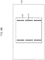
Fig. 8 is a schematic plan view illustrating another example of the thick copper substrate; and -
Figs. 9A and9B are schematic views illustrating a schematic configuration of an inverter according to a third embodiment. - Hereinafter, preferred embodiments will be explained in detail with reference to accompanying drawings.
- In this embodiment, a thick copper substrate is disclosed as a printed-circuit board and its configuration will be explained together with a manufacturing method thereof.
-
Figs. 1A to 1D andFigs. 2A to 2C are schematic sectional views illustrating the method of manufacturing the thick copper substrate according to this embodiment in order of steps. - First of all, as illustrated in
Fig. 1A , abase 1 of the thick copper substrate is prepared. - The
base 1 is formed of, for example, a plurality ofcopper layers 2 having a predetermined thickness of 70 µm or more stacked via insulating resin layers (for example, glass epoxy resin layers) 3. - Subsequently, as illustrated in
Fig. 1B , a PTH (Plated Through Hole) 11 is formed in thebase 1. - In detail, first, a first through
hole 11a is formed as a first hole in thebase 1. - Next, for example, a Cu layer is formed on the front surface and the rear surface of the
base 1 including an inner wall side surface of the first throughhole 11a by the plating method. The Cu layer is formed into a thickness of a value in a range of about 40 µm or more and 70 µm or less, for example, about 70 µm. Then, patterning is performed on the front surface and the rear surface of thebase 1 to remove a part of the Cu layer to thereby form a firstconductive layer 11b extending from the inner wall side surface of the first throughhole 11a up to parts on the front surface and on the rear surface of thebase 1. Note that it is also conceivable to form, as the firstconductive layer 11b, a stacked structure of Cu/Ni/Au (Cu is at the lowermost layer) in place of forming the CU layer. - Thus, the
PTH 11 including the firstconductive layer 11b covering the inner wall side surface of the first throughhole 11a is formed. - Subsequently, as illustrated in
Fig. 1C , aCu coin 12 is inserted into thePTH 11. - In this embodiment, the
Cu coin 12 being a columnar Cu material is used as a columnar electric conductor to be inserted into thePTH 11. TheCu coin 12 is formed to have a length slightly larger than the thickness of thebase 1, a cross-sectional shape in the same shape (circular shape here) as that of the first throughhole 11a, and a diameter slightly smaller than the diameter of the PTH 11 (diameter of the first throughhole 11a via the firstconductive layer 11b). TheCu coin 12 has a Vickers hardness of a value in a range of 30 Hv or more and 400 Hv or less, here, about 100 Hv. - Subsequently, as illustrated in
Fig. 1D , pressure is applied in a vertical direction to theCu coin 12. - In detail, the
base 1 with theCu coin 12 inserted into thePTH 11 is mounted and fixed onto a support table 10a. Apressing plate 10b is placed on the upper surface of thebase 1, and applies pressure downward. Thus, theCu coin 12 is reduced in length and expanded in diameter and thereby pressure-bonded to the firstconductive layer 11b. -
Figs. 3A and 3B are photographs indicating a pressure bonding state between the Cu layer formed by the plating method and the Cu coin, andFig. 3B indicates an enlarged appearance in a rectangular frame inFig. 3A . - Both of the first
conductive layer 11b and theCu coin 12 are made of the same Cu as a material in this embodiment, but the Cu material of theCu coin 12 changes in quality due to the application of the pressure. As a result, theCu coin 12 becomes different in crystalline state from the firstconductive layer 11b formed by the plating method, and its crystal grains become larger than those of the firstconductive layer 11b. Since theCu coin 12 is pressure-bonded to the firstconductive layer 11b, the firstconductive layer 11b and theCu coin 12 are brought into a close contact state without any gap therebetween on the inner wall side surface of thePTH 11. Further, since a pressure-bonding form of applying pressure to theCu coin 12 inserted into thePTH 11 is taken, a dent is generated in theCu coin 12 at an edge portion at the uppermost portion of thePTH 11. This dent can be confirmed also by observing thebase 1 from above. - Subsequently, as illustrated in
Figs. 2A, 2B , a second throughhole 12a is formed as a second hole in theCu coin 12. Thus, the thick copper substrate according to this embodiment is formed. - In detail, as illustrated in
Fig. 2A , the second throughhole 12a is formed using adrill 20 at a central portion of theCu coin 12. The drilling work is high in working accuracy and provides a pore diameter tolerance of about ± 30 µm or less. The second throughhole 12a is formed into, for example, a desired diameter of about 1.0 mm ± 30 µm. By forming the second throughhole 12a, a secondconductive layer 12b composed of Cu covering the side surface (inner wall side surface of the PTH 11) of the firstconductive layer 11b is formed as illustrated inFig. 2B . The secondconductive layer 12b is formed into a thickness of, for example, about 400 µm and is brought into close contact with and fixed to the side surface of the firstconductive layer 11b. - In this thick copper substrate, as illustrated in
Fig. 2C , a press-fit pin 13 as a terminal is inserted into and fixed to the second throughhole 12a. - The press-
fit pin 13 is made to be attachable to and detachable from the second throughhole 12a, and is brought into contact with and fix to, by its mechanical resilient restoring force, the side surface of the secondconductive layer 12b inside the second throughhole 12a in which the press-fit pin 13 is inserted. - In this embodiment, the second
conductive layer 12b in close contact with the side surface of the firstconductive layer 11b in thePTH 11 is formed without the firstconductive layer 11b being formed thick, thereby securing the conductive layer thickness on the inner wall side surface of thePTH 11. With this configuration, the secondconductive layer 12b protects the firstconductive layer 11b to suppress occurrence of cracks in the firstconductive layer 11b. Since the firstconductive layer 11b made by the plating method is formed thin, the firstconductive layer 11b can be easily formed into a fine pattern without deteriorating the productivity of plating. Even if a part of the secondconductive layer 12b is slightly damaged in inserting the press-fit pin 13, its influence is small because a sufficient conductive layer thickness by the firstconductive layer 11b and the secondconductive layer 12b is secured on the inner wall side surface of thePTH 11, so that the high connection reliability of the press-fit pin 13 is maintained. - The second
conductive layer 12b being a conductive layer with which the press-fit pin 13 comes into contact has a Vickers hardness set to a value in a range of 30 Hv or more and 400 Hv or less. The conductive layer is required to have hardness to withstand a load in inserting the press-fit pin 13 (at a level of maintaining desired connection reliability even when receiving pressure contact from the press-fit pin 13). The lower limit value of the hardness is evaluated to be about 30 Hv in Vickers hardness. On the other hand, if the conductive layer is too hard, appropriate press fitting of theCu coin 12 into thePTH 11 becomes difficult at the step inFig. 1D . The upper limit value of the hardness is evaluated to be about 400 Hv in Vickers hardness. In this embodiment, Cu being a conductive material having a Vickers hardness of a value in a range of 30 Hv or more and 400 Hv or less is used as the material of the secondconductive layer 12b. The secondconductive layer 12b is surely brought into close contact with and fixed to the firstconductive layer 11b to suppress occurrence of cracks in the firstconductive layer 11b and realize a thick copper substrate securing the connection reliability even if the press-fit pin 13 is inserted thereinto and fixed thereto. - The second
conductive layer 12b covering the side surface of the firstconductive layer 11b is formed to increase the conductive layer thickness on the inner wall side surface of thePTH 11, thereby increasing also the amount of current allowed to flow through onePTH 11. This makes it possible to reduce the number ofPTHs 11 required for desired current to flow, thereby improving the degree of freedom in substrate design. - As described above, according to this embodiment, the second
conductive layer 12b with a desired thickness is accurately secured on the inner wall side surface of thePTH 11 without using solder. This realizes a thick copper substrate in which the press-fit pin 13 can be inserted into and fixed to the second throughhole 12a with high connection reliability without damaging the firstconductive layer 11b. - Hereinafter, modified examples of the first embodiment will be explained.
- In a modified example 1, a thick copper substrate is disclosed as in the first embodiment, but is different from the first embodiment in that the second hole formed in the Cu coin is different.
-
Figs. 4A to 4C are schematic sectional views illustrating main steps of a method of manufacturing the thick copper substrate according to the modified example 1 of the first embodiment. Note that the same components as those of the thick copper substrate according to the first embodiment are denoted by the same numerals, and detailed explanation thereof will be omitted. - First of all, the steps in
Figs. 1A to 1D are performed as in the first embodiment. TheCu coin 12 is pressure-bonded to the firstconductive layer 11b. - Subsequently, as illustrated in
Figs. 4A, 4B , anon-through hole 12c not penetrating theCu coin 12 is formed as a second hole in theCu coin 12. Thus, the thick copper substrate according to this embodiment is formed. - In detail, as illustrated in
Fig. 4A , thenon-through hole 12c is formed by working a central portion of theCu coin 12 using thedrill 20 down to a middle in the length direction of theCu coin 12, for example, about half in the length direction. The drilling work is high in working accuracy and provides a pore diameter tolerance of about ± 30 µm or less. Thenon-through hole 12c is formed into, for example, a desired diameter of about 1.0 mm ± 30 µm. By forming thenon-through hole 12c, a secondconductive layer 12d composed of Cu having a bottom portion and covering the side surface (inner wall side surface of the PTH 11) of the firstconductive layer 11b is formed as illustrated inFig. 4B . The secondconductive layer 12d has a side surface portion formed into a thickness of, for example, about 400 µm and is brought into close contact with and fixed to the side surface of the firstconductive layer 11b. - In this thick copper substrate, as illustrated in
Fig. 4C , the press-fit pin 13 as the terminal is inserted into and fixed to thenon-through hole 12c. - The press-
fit pin 13 is made to be attachable to and detachable from thenon-through hole 12c, and is brought into contact with and fix to, by its mechanical resilient restoring force, the side surface of the secondconductive layer 12d inside thenon-through hole 12c in which the press-fit pin 13 is inserted. - In the modified example 1, the second
conductive layer 12d in close contact with the side surface of the firstconductive layer 11b in thePTH 11 is formed without the firstconductive layer 11b being formed thick, thereby securing the conductive layer thickness on the inner wall side surface of thePTH 11. With this configuration, the secondconductive layer 12d protects the firstconductive layer 11b to suppress occurrence of cracks in the firstconductive layer 11b. Since the firstconductive layer 11b made by the plating method is formed thin, the firstconductive layer 11b can be easily formed into a fine pattern without deteriorating the productivity of plating. Even if a part of the secondconductive layer 12d is slightly damaged in inserting the press-fit pin 13, its influence is small because a sufficient conductive layer thickness by the firstconductive layer 11b and the secondconductive layer 12d is secured on the inner wall side surface of thePTH 11, so that the high connection reliability of the press-fit pin 13 is maintained. - In the modified example 1, the conductive layer with which the press-
fit pin 13 comes into contact, here, the secondconductive layer 12d has a Vickers hardness set to a value in a range of 30 Hv or more and 400 Hv or less. The conductive layer is required to have hardness to withstand a load in inserting the press-fit pin 13 (at a level of maintaining desired connection reliability even when receiving pressure contact from the press-fit pin 13). The lower limit value of the hardness is evaluated to be about 30 Hv in Vickers hardness. On the other hand, if the conductive layer is too hard, appropriate press fitting of theCu coin 12 into thePTH 11 becomes difficult at the step inFig. 4B . The upper limit value of the hardness is evaluated to be about 400 Hv in Vickers hardness. In the modified example 1, Cu being a conductive material having a Vickers hardness of a value in a range of 30 Hv or more and 400 Hv or less is used as the material of the secondconductive layer 12d. The secondconductive layer 12d is surely brought into close contact with and fixed to the firstconductive layer 11b to suppress occurrence of cracks in the firstconductive layer 11b and realize a thick copper substrate securing the connection reliability even if the press-fit pin 13 is inserted thereinto and fixed thereto. - The second
conductive layer 12d covering the side surface of the firstconductive layer 11b is formed to increase the conductive layer thickness on the inner wall side surface of thePTH 11, thereby increasing also the amount of current allowed to flow through onePTH 11. This makes it possible to reduce the number ofPTHs 11 required for desired current to flow, thereby improving the degree of freedom in substrate design. - As described above, according to the modified example 1, the conductive layer (the second
conductive layer 12d) with a desired thickness is accurately secured on the inner wall side surface of thePTH 11 without using solder. This realizes a thick copper substrate in which the press-fit pin 13 can be inserted into and fixed to thenon-through hole 12c with high connection reliability without damaging the firstconductive layer 11b. - In a modified example 2, a thick copper substrate is disclosed as in the first embodiment, but is different from the first embodiment in that the conductive layer formed in the PTH is different.
-
Figs. 5A to 5C andFigs. 6A and 6B are schematic sectional views illustrating main steps of a method of manufacturing the thick copper substrate according to the modified example 2 of the first embodiment. Note that the same components as those of the thick copper substrate according to the first embodiment are denoted by the same numerals, and detailed explanation thereof will be omitted. - First of all, the steps in
Figs. 1A and 1B are performed as in the first embodiment. Thebase 1 is formed with thePTH 11. - Subsequently, as illustrated in
Fig. 5A , anAl alloy coin 21 is inserted into thePTH 11. - In this modified example, a conductive material differing from Cu of the first
conductive layer 11b, here, an Al alloy is employed and theAl alloy coin 21 being a columnar Al alloy material is used as the columnar electric conductor to be inserted into thePTH 11. TheAl alloy coin 21 is formed to have a length slightly larger than the thickness of thebase 1, a cross-sectional shape in the same shape (circular shape here) as that of the first throughhole 11a, and a diameter slightly smaller than the diameter of the PTH 11 (diameter of the first throughhole 11a via the firstconductive layer 11b). TheAl alloy coin 21 has a Vickers hardness of a value in a range of 30 Hv or more and 400 Hv or less, here, about 150 Hv. - Note that one kind selected from Al, Fe, a Cu alloy, a Ni alloy, a Fe alloy and the like other than the Al alloy may be employed as the conductive material of the columnar electric conductor, and a coin made of the conductive material may be used in this modified example.
- Subsequently, as illustrated in
Fig. 5B , pressure is applied in a vertical direction to theAl alloy coin 21. - In detail, the
base 1 with theAl alloy coin 21 inserted into thePTH 11 is mounted and fixed onto the support table 10a. Thepressing plate 10b is placed on the upper surface of thebase 1, and applies pressure downward. Thus, theAl alloy coin 21 is reduced in length and expanded in diameter and thereby pressure-bonded to the firstconductive layer 11b. - Since the first
conductive layer 11b and theAl alloy coin 21 are made of different conductive materials in the modified example 2, the pressure-bondedAl alloy coin 21 is different in crystalline state from the firstconductive layer 11b formed by the plating method. Since theAl alloy coin 21 is pressure-bonded to the firstconductive layer 11b, the firstconductive layer 11b and theAl alloy coin 21 are brought into a close contact state without any gap therebetween on the inner wall side surface of thePTH 11. Further, since a pressure-bonding form of applying pressure to theAl alloy coin 21 inserted into thePTH 11 is taken, a dent is generated in theAl alloy coin 21 at an edge portion at the uppermost portion of thePTH 11. This dent can be confirmed also by observing thebase 1 from above. - Subsequently, as illustrated in
Fig. 5C ,Fig. 6A , a second throughhole 21a is formed in theAl alloy coin 21. Thus, the thick copper substrate according to this modified example is formed. - In detail, as illustrated in
Fig. 5C , the second throughhole 21a is formed using thedrill 20 at a central portion of theAl alloy coin 21. The drilling work is high in working accuracy and provides a pore diameter tolerance of about ± 30 µm or less. The second throughhole 21a is formed into, for example, a desired diameter of about 1.0 mm ± 30 µm. By forming the second throughhole 21a, a secondconductive layer 21b composed of an Al alloy covering the side surface (inner wall side surface of the PTH 11) of the firstconductive layer 11b is formed as illustrated inFig. 6A . The secondconductive layer 21b is formed into a thickness of, for example, about 400 µm and is brought into close contact with and fixed to the side surface of the firstconductive layer 11b. - In this thick copper substrate, as illustrated in
Fig. 6B , the press-fit pin 13 as the terminal is inserted into and fixed to the second throughhole 21a. - The press-
fit pin 13 is made to be attachable to and detachable from the second throughhole 21a, and is brought into contact with and fix to, by its mechanical resilient restoring force, the side surface of the secondconductive layer 21b inside the second throughhole 21a in which the press-fit pin 13 is inserted. - In the modified example 2, the second
conductive layer 21b in close contact with the side surface of the firstconductive layer 11b in thePTH 11 is formed without the firstconductive layer 11b being formed thick, thereby securing the conductive layer thickness on the inner wall side surface of thePTH 11. With this configuration, the secondconductive layer 21b protects the firstconductive layer 11b to suppress occurrence of cracks in the firstconductive layer 11b. Since the firstconductive layer 11b made by the plating method is formed thin, the firstconductive layer 11b can be easily formed into a fine pattern without deteriorating the productivity of plating. Even if a part of the secondconductive layer 21b is slightly damaged in inserting the press-fit pin 13, its influence is small because a sufficient conductive layer thickness by the firstconductive layer 11b and the secondconductive layer 21b is secured on the inner wall side surface of thePTH 11, so that the high connection reliability of the press-fit pin 13 is maintained. - In the modified example 2, the conductive layer with which the press-
fit pin 13 comes into contact, here, the secondconductive layer 21b has a Vickers hardness set to a value in a range of 30 Hv or more and 400 Hv or less. The conductive layer is required to have hardness to withstand a load in inserting the press-fit pin 13 (at a level of maintaining desired connection reliability even when receiving pressure contact from the press-fit pin 13). The lower limit value of the hardness is evaluated to be about 30 Hv in Vickers hardness. On the other hand, if the conductive layer is too hard, appropriate press fitting of theAl alloy coin 21 into thePTH 11 becomes difficult at the step inFig. 5B . The upper limit value of this hardness is evaluated to be about 400 Hv in Vickers hardness. In the modified example 2, an Al alloy being a conductive material having a Vickers hardness of a value in a range of 30 Hv or more and 400 Hv or less is used as the material of the secondconductive layer 21b. The secondconductive layer 21b is surely brought into close contact with and fixed to the firstconductive layer 11b to suppress occurrence of cracks in the firstconductive layer 11b and realize a thick copper substrate securing the connection reliability even if the press-fit pin 13 is inserted thereinto and fixed thereto. - The second
conductive layer 21b covering the side surface of the firstconductive layer 11b is formed to increase the conductive layer thickness on the inner wall side surface of thePTH 11, thereby increasing also the amount of current allowed to flow through onePTH 11. This makes it possible to reduce the number ofPTHs 11 required for desired current to flow, thereby improving the degree of freedom in substrate design. - As described above, according to the modified example, the conductive layer (the second
conductive layer 21b) with a desired thickness is accurately secured on the inner wall side surface of thePTH 11 without using solder. This realizes a thick copper substrate in which the press-fit pin 13 can be inserted into and fixed to the second throughhole 21a with high connection reliability without damaging the firstconductive layer 11b. - In this embodiment, a thick copper substrate is disclosed as in the first embodiment, but is different from the first embodiment in that a terminal inserted into and fixed to a PTH is different.
-
Figs. 7A and 7B are schematic sectional views illustrating main steps of a method of manufacturing the thick copper substrate according to this embodiment. Note that the same components as those of the thick copper substrate according to the first embodiment are denoted by the same numerals, and detailed explanation thereof will be omitted. - In this embodiment, first of all, the steps in
Fig. 1A to Fig. 2B are performed as in the first embodiment. A secondconductive layer 12b including a second throughhole 12a is formed in abase 1 to cover an inner wall side surface of a firstconductive layer 11b of thePTH 11. - Subsequently, as illustrated in
Fig. 7A , athread groove 12e is formed on an inner wall side surface of the second throughhole 12a. Thus, the thick copper substrate according to this embodiment is formed. - In detail, the
thread groove 12e being a female thread is formed on the inner wall side surface (side surface of the secondconductive layer 12b) of the second throughhole 12a by shaving the second throughhole 12a. In this event, it is also possible to repair the thread groove by helical insert processing. - In this thick copper substrate, a
screw 22 as a terminal is engaged and fixed to the inside of the second throughhole 12a as illustrated inFig. 7B . - In detail, the
screw 22 is inserted into and fixed to the second throughhole 12a having the inner wall side surface formed with thethread groove 12e. In this case, thescrew 22 may be used also as a fixing member of the thick copper substrate with another not-illustrated printed-circuit board or the like to connect with the printed-circuit board or the like. - In this embodiment, the second
conductive layer 12b in close contact with the side surface of the firstconductive layer 11b in thePTH 11 is formed without the firstconductive layer 11b being formed thick, thereby securing the conductive layer thickness on the inner wall side surface of thePTH 11. With this configuration, the secondconductive layer 12b protects the firstconductive layer 11b to suppress occurrence of cracks in the firstconductive layer 11b. Since the firstconductive layer 11b made by the plating method is formed thin, the firstconductive layer 11b can be easily formed into a fine pattern without deteriorating the productivity of plating. Even if a part of the secondconductive layer 12b is slightly damaged in forming thethread groove 12e, its influence is small because a sufficient conductive layer thickness by the firstconductive layer 11b and the secondconductive layer 12b is secured on the inner wall side surface of thePTH 11, so that the high connection reliability of thescrew 22 is maintained. - In this embodiment, a conductive layer to which the
screw 22 is engaged and fixed, here, the secondconductive layer 12b has a Vickers hardness set to a value in a range of 30 Hv or more and 400 Hv or less. The conductive layer is required to have hardness to withstand the processing of forming thethread groove 12e. The lower limit value of the hardness is evaluated to be about 30 Hv in Vickers hardness. On the other hand, if the conductive layer is too hard, appropriate press fitting into thePTH 11 becomes difficult at the step inFig. 1D . The upper limit value of the hardness is evaluated to be about 400 Hv in Vickers hardness. In this embodiment, Cu being a conductive material having a Vickers hardness of a value in a range of 30 Hv or more and 400 Hv or less is used as the material of the secondconductive layer 12b. The secondconductive layer 12b is surely brought into close contact with and fixed to the firstconductive layer 11b to suppress occurrence of cracks in the firstconductive layer 11b and realize a thick copper substrate securing the connection reliability even if thethread groove 12e is formed therein. - The second
conductive layer 12b covering the side surface of the firstconductive layer 11b is formed to increase the conductive layer thickness on the inner wall side surface of thePTH 11, thereby increasing also the amount of current allowed to flow through onePTH 11. This makes it possible to reduce the number ofPTHs 11 required for desired current to flow, thereby improving the degree of freedom in substrate design. - Since only the conductive layer on the inner wall side surface of the
PTH 11 of the secondconductive layer 12b is formed thick without the firstconductive layer 11b being formed thick, the firstconductive layer 11b can be easily formed into a fine pattern without deteriorating the productivity of plating. - As described above, according to this embodiment, the conductive layer (second
conductive layer 12b) with a desired thickness is accurately secured on the inner wall side surface of thePTH 11 without using solder (having a Vickers hardness of 20 Hv or less). This makes it possible to form thethread groove 12e in the second throughhole 12a with high reliability and insert and fix thescrew 22 thereto, and realize direct screw fixation to the printed-circuit board or the like with the terminal that is impossible in the prior art, leading to expectation in expansion to various use scenes. - Note that one kind of conductive material selected from Al, Ni, Fe, a Cu alloy, an Al alloy, a Ni alloy, a Fe alloy and the like in place of and different from Cu may be employed as the second conductive layer formed in the
PTH 11 also in the second embodiment, as in the modified example 2 of the first embodiment. - In the modified example 2 of the first embodiment and the second embodiment, a non-through hole not penetrating the Cu coin 12 (A1 alloy coin 21) may be formed as a second hole in the Cu coin 12 (A1 alloy coin 21) as in the modified example 1 of the first embodiment.
- The second through
hole 12a (21a) or thenon-through hole 12c is formed in a circular shape corresponding to the press-fit pin 13 (screw 22) in the first and second embodiments and modified examples, but the first throughhole 11a may be formed in a shape different from that of the second throughhole 12a (21a) or thenon-through hole 12c. Conceivable examples of the shape include a rectangular shape, an elliptical shape and so on. In the case of the rectangular shape, the shape is desirably made to have corners rounded in order to prevent breakage or the like in press-fitting the coin made of conductive material into the PTH. - One example is illustrated in
Fig. 8 . The case of the first embodiment is exemplified here. Press-fit pins 13 inserted into a plurality of adjacent second throughholes 12a formed in the same secondconductive layer 12b are set at the same potential. - In the case of
Fig. 8 , the first throughhole 11a is formed, for example, into a rectangular shape with rounded corners, the firstconductive layer 11b is formed by plating, and then theCu coin 12 is inserted into thePTH 11. TheCu coin 12 is a columnar Cu material and has a length slightly larger than the thickness of thebase 1, a cross-sectional shape being the same rectangular shape as that of the first throughhole 11a, and a size slightly smaller than the size of thePTH 11. Pressure is applied to theCu coin 12 from above and below to pressure-bond theCu coin 12 to the firstconductive layer 11b. Then, a plurality of (four, here) second throughholes 12a are formed in theCu coin 12. - In this embodiment, an inverter is disclosed to which the thick copper substrate according to the first embodiment or its modified example is applied.
-
Figs. 9A and9B are schematic views illustrating a schematic configuration of the inverter according to this embodiment,Fig. 9A is a sectional view andFig. 9B is a plan view. - This inverter includes a
power module 31, athick copper substrate 32 on which various components are mounted. - The
power module 31 is a power semiconductor element made by combining a plurality of functional elements such as a transistor, a diode, a thyristor and so on. - The
thick copper substrate 32 is a thick copper substrate according to the first embodiment or its modified example.Figs. 9A and9B illustrate, for example, the thick copper substrate according to the first embodiment. On the surface of thethick copper substrate 32, aninput terminal 33, anoutput terminal 34, aninput capacitor 35, a three-layer reactor 36, acontrol unit 37 of thepower module 31, and a controlsignal transmission unit 38 are mounted. Thecontrol unit 37 is electrically connected to the top of thethick copper substrate 32 viaconnectors 39a, and the controlsignal transmission unit 38 is electrically connected to the top of thecontrol unit 37 viaconnectors 39b. - The
thick copper substrate 32 is formed with a plurality of PTHs, and the press-fit pins 13 are inserted into and fixed to the PTHs respectively. These press-fit pins 13 electrically connect thepower module 31 with thethick copper substrate 32. - According to this embodiment, a highly reliable inverter including the
thick copper substrate 32 in which a conductive layer having a desired thickness is secured with high accuracy on the inner wall side surface of the through hole without using solder and the terminal can be inserted and fixed with high reliability without damaging the conductive layer, is realized. - In one aspect, a substrate in which a conductive layer having a desired thickness is secured with high accuracy on an inner wall side surface of a through hole without using solder and a terminal can be inserted into and fixed to the through hole with high connection reliability, is realized.
Claims (15)
- A method of manufacturing a substrate, the method comprising:forming a first hole, the first hole penetrating a base;forming a conductive layer, the conductive layer covering an inner wall side surface of the first hole;inserting a columnar electric conductor into the first hole formed with the conductive layer;applying pressure in a vertical direction to the columnar electric conductor; andforming a second hole in the columnar electric conductor.
- The method of manufacturing a substrate according to claim 1, wherein the columnar electric conductor is made of a same conductive material as a conductive material of the conductive layer or a conductive material different from the conductive material of the conductive layer.
- The method of manufacturing a substrate according to claim 1 or 2, wherein the columnar electric conductor has a side surface brought into close contact with the conductive layer.
- The method of manufacturing a substrate according to any one of claims 1 to 3, wherein the columnar electric conductor has a diameter smaller than a diameter of the first hole via the conductive layer, and has a length larger than a thickness of the base.
- The method of manufacturing a substrate according to any one of claims 1 to 4, wherein the columnar electric conductor has a Vickers hardness of a value of 30 Hv or more and a value of 400 Hv or less.
- The method of manufacturing a substrate according to any one of claims 1 to 5, wherein the second hole is a hole penetrating the columnar electric conductor.
- The method of manufacturing a substrate according to any one of claims 1 to 5, wherein the second hole is a hole not penetrating the columnar electric conductor.
- The method of manufacturing a substrate according to any one of claims 1 to 7, wherein the columnar electric conductor includes a plurality of the second holes.
- The method of manufacturing a substrate according to any one of claims 1 to 8, further comprising:forming a thread groove on an inner wall side surface of the second hole.
- A substrate comprising:a base including a first hole penetrating the base;a first conductive layer covering an inner wall side surface of the first hole; anda second conductive layer covering a side surface of the first conductive layer and including a second hole,wherein the second conductive layer is different in crystalline structure from the first conductive layer and has a Vickers hardness of a value of 30 Hv or more.
- The substrate according to claim 10, wherein the second conductive layer is in close contact with the first conductive layer.
- The substrate according to claim 10 or 11, wherein the second conductive layer is made of a same conductive material as a conductive material of the first conductive layer and has a crystal grain larger than a crystal grain of the first conductive layer.
- The substrate according to claim 10 or 11, wherein the second conductive layer is made of a conductive material different from a conductive material of the first conductive layer.
- The substrate according to any one of claims 10 to 13, wherein the second conductive layer has a Vickers hardness of a value of 400 Hv or less.
- The substrate according to any one of claims 10 to 14, wherein:the second hole is in a circular shape; andthe first hole is in a shape different from the shape of the second hole.
Applications Claiming Priority (1)
| Application Number | Priority Date | Filing Date | Title |
|---|---|---|---|
| JP2016235436A JP6778598B2 (en) | 2016-12-02 | 2016-12-02 | Substrate manufacturing method and substrate |
Publications (2)
| Publication Number | Publication Date |
|---|---|
| EP3331332A1 true EP3331332A1 (en) | 2018-06-06 |
| EP3331332B1 EP3331332B1 (en) | 2021-03-17 |
Family
ID=60331461
Family Applications (1)
| Application Number | Title | Priority Date | Filing Date |
|---|---|---|---|
| EP17201822.8A Active EP3331332B1 (en) | 2016-12-02 | 2017-11-15 | Method of manufacturing substrate |
Country Status (3)
| Country | Link |
|---|---|
| US (1) | US10009998B1 (en) |
| EP (1) | EP3331332B1 (en) |
| JP (1) | JP6778598B2 (en) |
Cited By (1)
| Publication number | Priority date | Publication date | Assignee | Title |
|---|---|---|---|---|
| CN108966505A (en) * | 2018-08-28 | 2018-12-07 | 郑州云海信息技术有限公司 | The method of pcb board installation via hole |
Families Citing this family (4)
| Publication number | Priority date | Publication date | Assignee | Title |
|---|---|---|---|---|
| KR102495931B1 (en) * | 2015-12-15 | 2023-02-02 | 엘지디스플레이 주식회사 | Printed circuit board and display device including the same |
| US12171064B2 (en) | 2021-03-04 | 2024-12-17 | Raytheon Company | Interconnect and method for manufacturing the same |
| CN113286435A (en) * | 2021-05-25 | 2021-08-20 | 胜宏科技(惠州)股份有限公司 | Method for plating copper in aluminum plate hole |
| JP2025150877A (en) * | 2024-03-27 | 2025-10-09 | 株式会社デンソー | electronic equipment |
Citations (8)
| Publication number | Priority date | Publication date | Assignee | Title |
|---|---|---|---|---|
| JPH0496392A (en) * | 1990-08-14 | 1992-03-27 | Nec Corp | Mounting method for electric component and eyeletused therefor |
| US5257452A (en) * | 1991-05-27 | 1993-11-02 | Hitachi, Ltd. | Methods of recovering a multi-layer printed circuit board |
| JPH05304223A (en) | 1992-04-24 | 1993-11-16 | Citizen Watch Co Ltd | Manufacture of electronic component mounting board |
| JP2005116463A (en) * | 2003-10-10 | 2005-04-28 | Toyota Motor Corp | Through-hole sleeve and method of adding protection circuit |
| JP2006156435A (en) | 2004-11-25 | 2006-06-15 | Shinko Electric Ind Co Ltd | Wiring board manufacturing method |
| JP2006319044A (en) * | 2005-05-11 | 2006-11-24 | Nissan Motor Co Ltd | Board mounting structure, board mounting method, and connection pins used in these |
| JP2007180079A (en) | 2005-12-27 | 2007-07-12 | Cmk Corp | Printed wiring board for press-fit bonding and manufacturing method thereof |
| JP2009016662A (en) | 2007-07-06 | 2009-01-22 | Yazaki Corp | Metal core board |
-
2016
- 2016-12-02 JP JP2016235436A patent/JP6778598B2/en active Active
-
2017
- 2017-11-08 US US15/806,385 patent/US10009998B1/en active Active
- 2017-11-15 EP EP17201822.8A patent/EP3331332B1/en active Active
Patent Citations (8)
| Publication number | Priority date | Publication date | Assignee | Title |
|---|---|---|---|---|
| JPH0496392A (en) * | 1990-08-14 | 1992-03-27 | Nec Corp | Mounting method for electric component and eyeletused therefor |
| US5257452A (en) * | 1991-05-27 | 1993-11-02 | Hitachi, Ltd. | Methods of recovering a multi-layer printed circuit board |
| JPH05304223A (en) | 1992-04-24 | 1993-11-16 | Citizen Watch Co Ltd | Manufacture of electronic component mounting board |
| JP2005116463A (en) * | 2003-10-10 | 2005-04-28 | Toyota Motor Corp | Through-hole sleeve and method of adding protection circuit |
| JP2006156435A (en) | 2004-11-25 | 2006-06-15 | Shinko Electric Ind Co Ltd | Wiring board manufacturing method |
| JP2006319044A (en) * | 2005-05-11 | 2006-11-24 | Nissan Motor Co Ltd | Board mounting structure, board mounting method, and connection pins used in these |
| JP2007180079A (en) | 2005-12-27 | 2007-07-12 | Cmk Corp | Printed wiring board for press-fit bonding and manufacturing method thereof |
| JP2009016662A (en) | 2007-07-06 | 2009-01-22 | Yazaki Corp | Metal core board |
Cited By (1)
| Publication number | Priority date | Publication date | Assignee | Title |
|---|---|---|---|---|
| CN108966505A (en) * | 2018-08-28 | 2018-12-07 | 郑州云海信息技术有限公司 | The method of pcb board installation via hole |
Also Published As
| Publication number | Publication date |
|---|---|
| JP6778598B2 (en) | 2020-11-04 |
| JP2018093068A (en) | 2018-06-14 |
| EP3331332B1 (en) | 2021-03-17 |
| US10009998B1 (en) | 2018-06-26 |
| US20180160547A1 (en) | 2018-06-07 |
Similar Documents
| Publication | Publication Date | Title |
|---|---|---|
| EP3331332A1 (en) | Method of manufacturing substrate and substrate | |
| US8449339B2 (en) | Connector assembly and method of manufacture | |
| EP2001274A2 (en) | Manufacturing method of substrate with through electrodes | |
| US20030128526A1 (en) | Multilayer ceramic electronic component and manufacturing method thereof | |
| US20180247768A1 (en) | Electrical component and a method for producing an electrical component | |
| US20140124255A1 (en) | Method for manufacturing electronic component-embedded substrate and electronic component-embedded substrate | |
| US20170309558A1 (en) | Interposer and method for manufacturing interposer | |
| US20100032196A1 (en) | Multilayer wiring board, semiconductor package and method of manufacturing the same | |
| CN109390290A (en) | Semiconductor subassembly | |
| CN101295699A (en) | Substrate with leads, wiring substrate and semiconductor device | |
| US20190254164A1 (en) | Circuit board, method of manufacturing circuit board, and electronic device | |
| EP3499649A1 (en) | Power semiconductor module arrangement | |
| EP3822997B1 (en) | Busbar laminate, electronic component mounting module including same, and method of manufacturing busbar laminate | |
| JP4759041B2 (en) | Electronic component built-in multilayer board | |
| US10658200B2 (en) | Thin film component sheet, board with built-in electronic component, and method of manufacturing the thin film component sheet | |
| JP6673304B2 (en) | Multilayer board | |
| US10163746B2 (en) | Semiconductor package with improved signal stability and method of manufacturing the same | |
| CN106852060B (en) | Screw supporting device and fixing method of PCB and screw | |
| US7656679B2 (en) | Multi-layer substrate and manufacture method thereof | |
| KR20240132188A (en) | Method of manufacturing the printed circuit board embedded with wafer level component | |
| JP5277754B2 (en) | Flip connection mounting body and method of manufacturing flip connection mounting body | |
| US12494419B2 (en) | Integrated circuit package with warpage control using cavity formed in laminated substrate below the integrated circuit die | |
| CN210129511U (en) | High frequency module | |
| JP4841234B2 (en) | Manufacturing method of wiring substrate with built-in via array capacitor | |
| JP7419738B2 (en) | Thin film capacitors and circuit boards containing them |
Legal Events
| Date | Code | Title | Description |
|---|---|---|---|
| PUAI | Public reference made under article 153(3) epc to a published international application that has entered the european phase |
Free format text: ORIGINAL CODE: 0009012 |
|
| STAA | Information on the status of an ep patent application or granted ep patent |
Free format text: STATUS: THE APPLICATION HAS BEEN PUBLISHED |
|
| AK | Designated contracting states |
Kind code of ref document: A1 Designated state(s): AL AT BE BG CH CY CZ DE DK EE ES FI FR GB GR HR HU IE IS IT LI LT LU LV MC MK MT NL NO PL PT RO RS SE SI SK SM TR |
|
| AX | Request for extension of the european patent |
Extension state: BA ME |
|
| STAA | Information on the status of an ep patent application or granted ep patent |
Free format text: STATUS: REQUEST FOR EXAMINATION WAS MADE |
|
| 17P | Request for examination filed |
Effective date: 20180803 |
|
| RBV | Designated contracting states (corrected) |
Designated state(s): AL AT BE BG CH CY CZ DE DK EE ES FI FR GB GR HR HU IE IS IT LI LT LU LV MC MK MT NL NO PL PT RO RS SE SI SK SM TR |
|
| RAP1 | Party data changed (applicant data changed or rights of an application transferred) |
Owner name: FUJITSU INTERCONNECT TECHNOLOGIES LIMITED |
|
| GRAP | Despatch of communication of intention to grant a patent |
Free format text: ORIGINAL CODE: EPIDOSNIGR1 |
|
| STAA | Information on the status of an ep patent application or granted ep patent |
Free format text: STATUS: GRANT OF PATENT IS INTENDED |
|
| RIC1 | Information provided on ipc code assigned before grant |
Ipc: H05K 3/00 20060101ALN20201027BHEP Ipc: H05K 3/40 20060101ALI20201027BHEP Ipc: H05K 1/11 20060101AFI20201027BHEP Ipc: H05K 3/30 20060101ALN20201027BHEP |
|
| INTG | Intention to grant announced |
Effective date: 20201125 |
|
| GRAS | Grant fee paid |
Free format text: ORIGINAL CODE: EPIDOSNIGR3 |
|
| GRAA | (expected) grant |
Free format text: ORIGINAL CODE: 0009210 |
|
| STAA | Information on the status of an ep patent application or granted ep patent |
Free format text: STATUS: THE PATENT HAS BEEN GRANTED |
|
| AK | Designated contracting states |
Kind code of ref document: B1 Designated state(s): AL AT BE BG CH CY CZ DE DK EE ES FI FR GB GR HR HU IE IS IT LI LT LU LV MC MK MT NL NO PL PT RO RS SE SI SK SM TR |
|
| REG | Reference to a national code |
Ref country code: GB Ref legal event code: FG4D |
|
| RIN1 | Information on inventor provided before grant (corrected) |
Inventor name: HASEGAWA, SATORU Inventor name: MIYAO, HIROSHI Inventor name: OZAKI, NORIKAZU |
|
| REG | Reference to a national code |
Ref country code: CH Ref legal event code: EP |
|
| REG | Reference to a national code |
Ref country code: DE Ref legal event code: R096 Ref document number: 602017034665 Country of ref document: DE |
|
| REG | Reference to a national code |
Ref country code: IE Ref legal event code: FG4D |
|
| REG | Reference to a national code |
Ref country code: AT Ref legal event code: REF Ref document number: 1373513 Country of ref document: AT Kind code of ref document: T Effective date: 20210415 |
|
| REG | Reference to a national code |
Ref country code: LT Ref legal event code: MG9D |
|
| PG25 | Lapsed in a contracting state [announced via postgrant information from national office to epo] |
Ref country code: HR Free format text: LAPSE BECAUSE OF FAILURE TO SUBMIT A TRANSLATION OF THE DESCRIPTION OR TO PAY THE FEE WITHIN THE PRESCRIBED TIME-LIMIT Effective date: 20210317 Ref country code: FI Free format text: LAPSE BECAUSE OF FAILURE TO SUBMIT A TRANSLATION OF THE DESCRIPTION OR TO PAY THE FEE WITHIN THE PRESCRIBED TIME-LIMIT Effective date: 20210317 Ref country code: GR Free format text: LAPSE BECAUSE OF FAILURE TO SUBMIT A TRANSLATION OF THE DESCRIPTION OR TO PAY THE FEE WITHIN THE PRESCRIBED TIME-LIMIT Effective date: 20210618 Ref country code: NO Free format text: LAPSE BECAUSE OF FAILURE TO SUBMIT A TRANSLATION OF THE DESCRIPTION OR TO PAY THE FEE WITHIN THE PRESCRIBED TIME-LIMIT Effective date: 20210617 Ref country code: BG Free format text: LAPSE BECAUSE OF FAILURE TO SUBMIT A TRANSLATION OF THE DESCRIPTION OR TO PAY THE FEE WITHIN THE PRESCRIBED TIME-LIMIT Effective date: 20210617 |
|
| REG | Reference to a national code |
Ref country code: AT Ref legal event code: MK05 Ref document number: 1373513 Country of ref document: AT Kind code of ref document: T Effective date: 20210317 |
|
| PG25 | Lapsed in a contracting state [announced via postgrant information from national office to epo] |
Ref country code: LV Free format text: LAPSE BECAUSE OF FAILURE TO SUBMIT A TRANSLATION OF THE DESCRIPTION OR TO PAY THE FEE WITHIN THE PRESCRIBED TIME-LIMIT Effective date: 20210317 Ref country code: RS Free format text: LAPSE BECAUSE OF FAILURE TO SUBMIT A TRANSLATION OF THE DESCRIPTION OR TO PAY THE FEE WITHIN THE PRESCRIBED TIME-LIMIT Effective date: 20210317 Ref country code: SE Free format text: LAPSE BECAUSE OF FAILURE TO SUBMIT A TRANSLATION OF THE DESCRIPTION OR TO PAY THE FEE WITHIN THE PRESCRIBED TIME-LIMIT Effective date: 20210317 |
|
| PG25 | Lapsed in a contracting state [announced via postgrant information from national office to epo] |
Ref country code: NL Free format text: LAPSE BECAUSE OF FAILURE TO SUBMIT A TRANSLATION OF THE DESCRIPTION OR TO PAY THE FEE WITHIN THE PRESCRIBED TIME-LIMIT Effective date: 20210317 |
|
| PG25 | Lapsed in a contracting state [announced via postgrant information from national office to epo] |
Ref country code: CZ Free format text: LAPSE BECAUSE OF FAILURE TO SUBMIT A TRANSLATION OF THE DESCRIPTION OR TO PAY THE FEE WITHIN THE PRESCRIBED TIME-LIMIT Effective date: 20210317 Ref country code: EE Free format text: LAPSE BECAUSE OF FAILURE TO SUBMIT A TRANSLATION OF THE DESCRIPTION OR TO PAY THE FEE WITHIN THE PRESCRIBED TIME-LIMIT Effective date: 20210317 Ref country code: LT Free format text: LAPSE BECAUSE OF FAILURE TO SUBMIT A TRANSLATION OF THE DESCRIPTION OR TO PAY THE FEE WITHIN THE PRESCRIBED TIME-LIMIT Effective date: 20210317 Ref country code: AT Free format text: LAPSE BECAUSE OF FAILURE TO SUBMIT A TRANSLATION OF THE DESCRIPTION OR TO PAY THE FEE WITHIN THE PRESCRIBED TIME-LIMIT Effective date: 20210317 Ref country code: SM Free format text: LAPSE BECAUSE OF FAILURE TO SUBMIT A TRANSLATION OF THE DESCRIPTION OR TO PAY THE FEE WITHIN THE PRESCRIBED TIME-LIMIT Effective date: 20210317 |
|
| PG25 | Lapsed in a contracting state [announced via postgrant information from national office to epo] |
Ref country code: IS Free format text: LAPSE BECAUSE OF FAILURE TO SUBMIT A TRANSLATION OF THE DESCRIPTION OR TO PAY THE FEE WITHIN THE PRESCRIBED TIME-LIMIT Effective date: 20210717 Ref country code: PT Free format text: LAPSE BECAUSE OF FAILURE TO SUBMIT A TRANSLATION OF THE DESCRIPTION OR TO PAY THE FEE WITHIN THE PRESCRIBED TIME-LIMIT Effective date: 20210719 Ref country code: PL Free format text: LAPSE BECAUSE OF FAILURE TO SUBMIT A TRANSLATION OF THE DESCRIPTION OR TO PAY THE FEE WITHIN THE PRESCRIBED TIME-LIMIT Effective date: 20210317 Ref country code: RO Free format text: LAPSE BECAUSE OF FAILURE TO SUBMIT A TRANSLATION OF THE DESCRIPTION OR TO PAY THE FEE WITHIN THE PRESCRIBED TIME-LIMIT Effective date: 20210317 Ref country code: SK Free format text: LAPSE BECAUSE OF FAILURE TO SUBMIT A TRANSLATION OF THE DESCRIPTION OR TO PAY THE FEE WITHIN THE PRESCRIBED TIME-LIMIT Effective date: 20210317 |
|
| REG | Reference to a national code |
Ref country code: DE Ref legal event code: R097 Ref document number: 602017034665 Country of ref document: DE |
|
| PLBE | No opposition filed within time limit |
Free format text: ORIGINAL CODE: 0009261 |
|
| STAA | Information on the status of an ep patent application or granted ep patent |
Free format text: STATUS: NO OPPOSITION FILED WITHIN TIME LIMIT |
|
| PG25 | Lapsed in a contracting state [announced via postgrant information from national office to epo] |
Ref country code: AL Free format text: LAPSE BECAUSE OF FAILURE TO SUBMIT A TRANSLATION OF THE DESCRIPTION OR TO PAY THE FEE WITHIN THE PRESCRIBED TIME-LIMIT Effective date: 20210317 Ref country code: DK Free format text: LAPSE BECAUSE OF FAILURE TO SUBMIT A TRANSLATION OF THE DESCRIPTION OR TO PAY THE FEE WITHIN THE PRESCRIBED TIME-LIMIT Effective date: 20210317 Ref country code: ES Free format text: LAPSE BECAUSE OF FAILURE TO SUBMIT A TRANSLATION OF THE DESCRIPTION OR TO PAY THE FEE WITHIN THE PRESCRIBED TIME-LIMIT Effective date: 20210317 |
|
| 26N | No opposition filed |
Effective date: 20211220 |
|
| PG25 | Lapsed in a contracting state [announced via postgrant information from national office to epo] |
Ref country code: SI Free format text: LAPSE BECAUSE OF FAILURE TO SUBMIT A TRANSLATION OF THE DESCRIPTION OR TO PAY THE FEE WITHIN THE PRESCRIBED TIME-LIMIT Effective date: 20210317 |
|
| PG25 | Lapsed in a contracting state [announced via postgrant information from national office to epo] |
Ref country code: IT Free format text: LAPSE BECAUSE OF FAILURE TO SUBMIT A TRANSLATION OF THE DESCRIPTION OR TO PAY THE FEE WITHIN THE PRESCRIBED TIME-LIMIT Effective date: 20210317 |
|
| PG25 | Lapsed in a contracting state [announced via postgrant information from national office to epo] |
Ref country code: IS Free format text: LAPSE BECAUSE OF FAILURE TO SUBMIT A TRANSLATION OF THE DESCRIPTION OR TO PAY THE FEE WITHIN THE PRESCRIBED TIME-LIMIT Effective date: 20210717 |
|
| PG25 | Lapsed in a contracting state [announced via postgrant information from national office to epo] |
Ref country code: MC Free format text: LAPSE BECAUSE OF FAILURE TO SUBMIT A TRANSLATION OF THE DESCRIPTION OR TO PAY THE FEE WITHIN THE PRESCRIBED TIME-LIMIT Effective date: 20210317 |
|
| REG | Reference to a national code |
Ref country code: CH Ref legal event code: PL |
|
| GBPC | Gb: european patent ceased through non-payment of renewal fee |
Effective date: 20211115 |
|
| PG25 | Lapsed in a contracting state [announced via postgrant information from national office to epo] |
Ref country code: LU Free format text: LAPSE BECAUSE OF NON-PAYMENT OF DUE FEES Effective date: 20211115 Ref country code: BE Free format text: LAPSE BECAUSE OF NON-PAYMENT OF DUE FEES Effective date: 20211130 |
|
| REG | Reference to a national code |
Ref country code: BE Ref legal event code: MM Effective date: 20211130 |
|
| PG25 | Lapsed in a contracting state [announced via postgrant information from national office to epo] |
Ref country code: LI Free format text: LAPSE BECAUSE OF NON-PAYMENT OF DUE FEES Effective date: 20211130 Ref country code: CH Free format text: LAPSE BECAUSE OF NON-PAYMENT OF DUE FEES Effective date: 20211130 |
|
| PG25 | Lapsed in a contracting state [announced via postgrant information from national office to epo] |
Ref country code: IE Free format text: LAPSE BECAUSE OF NON-PAYMENT OF DUE FEES Effective date: 20211115 Ref country code: GB Free format text: LAPSE BECAUSE OF NON-PAYMENT OF DUE FEES Effective date: 20211115 |
|
| PG25 | Lapsed in a contracting state [announced via postgrant information from national office to epo] |
Ref country code: FR Free format text: LAPSE BECAUSE OF NON-PAYMENT OF DUE FEES Effective date: 20211130 |
|
| PG25 | Lapsed in a contracting state [announced via postgrant information from national office to epo] |
Ref country code: HU Free format text: LAPSE BECAUSE OF FAILURE TO SUBMIT A TRANSLATION OF THE DESCRIPTION OR TO PAY THE FEE WITHIN THE PRESCRIBED TIME-LIMIT; INVALID AB INITIO Effective date: 20171115 |
|
| PG25 | Lapsed in a contracting state [announced via postgrant information from national office to epo] |
Ref country code: CY Free format text: LAPSE BECAUSE OF FAILURE TO SUBMIT A TRANSLATION OF THE DESCRIPTION OR TO PAY THE FEE WITHIN THE PRESCRIBED TIME-LIMIT Effective date: 20210317 |
|
| REG | Reference to a national code |
Ref country code: DE Ref legal event code: R081 Ref document number: 602017034665 Country of ref document: DE Owner name: FICT LIMITED, JP Free format text: FORMER OWNER: FUJITSU INTERCONNECT TECHNOLOGIES LTD., NAGANO, JP |
|
| REG | Reference to a national code |
Ref country code: DE Ref legal event code: R081 Ref document number: 602017034665 Country of ref document: DE Owner name: FICT LIMITED, JP Free format text: FORMER OWNER: FICT LTD., NAGANO-SHI, JP |
|
| PG25 | Lapsed in a contracting state [announced via postgrant information from national office to epo] |
Ref country code: MK Free format text: LAPSE BECAUSE OF FAILURE TO SUBMIT A TRANSLATION OF THE DESCRIPTION OR TO PAY THE FEE WITHIN THE PRESCRIBED TIME-LIMIT Effective date: 20210317 |
|
| PG25 | Lapsed in a contracting state [announced via postgrant information from national office to epo] |
Ref country code: TR Free format text: LAPSE BECAUSE OF FAILURE TO SUBMIT A TRANSLATION OF THE DESCRIPTION OR TO PAY THE FEE WITHIN THE PRESCRIBED TIME-LIMIT Effective date: 20210317 |
|
| PG25 | Lapsed in a contracting state [announced via postgrant information from national office to epo] |
Ref country code: MT Free format text: LAPSE BECAUSE OF FAILURE TO SUBMIT A TRANSLATION OF THE DESCRIPTION OR TO PAY THE FEE WITHIN THE PRESCRIBED TIME-LIMIT Effective date: 20210317 |
|
| PGFP | Annual fee paid to national office [announced via postgrant information from national office to epo] |
Ref country code: DE Payment date: 20251119 Year of fee payment: 9 |
|
| REG | Reference to a national code |
Ref country code: DE Ref legal event code: R081 Ref document number: 602017034665 Country of ref document: DE Owner name: FICT LIMITED, JP Free format text: FORMER OWNER: FICT LIMITED, NAGANO-SHI, JP |