EP3331147A1 - Converter circuit and current sensing - Google Patents
Converter circuit and current sensing Download PDFInfo
- Publication number
- EP3331147A1 EP3331147A1 EP17201473.0A EP17201473A EP3331147A1 EP 3331147 A1 EP3331147 A1 EP 3331147A1 EP 17201473 A EP17201473 A EP 17201473A EP 3331147 A1 EP3331147 A1 EP 3331147A1
- Authority
- EP
- European Patent Office
- Prior art keywords
- converter circuit
- converter stage
- switch
- electrical energy
- current sensing
- Prior art date
- Legal status (The legal status is an assumption and is not a legal conclusion. Google has not performed a legal analysis and makes no representation as to the accuracy of the status listed.)
- Granted
Links
Images





Classifications
-
- H—ELECTRICITY
- H02—GENERATION; CONVERSION OR DISTRIBUTION OF ELECTRIC POWER
- H02M—APPARATUS FOR CONVERSION BETWEEN AC AND AC, BETWEEN AC AND DC, OR BETWEEN DC AND DC, AND FOR USE WITH MAINS OR SIMILAR POWER SUPPLY SYSTEMS; CONVERSION OF DC OR AC INPUT POWER INTO SURGE OUTPUT POWER; CONTROL OR REGULATION THEREOF
- H02M3/00—Conversion of DC power input into DC power output
- H02M3/22—Conversion of DC power input into DC power output with intermediate conversion into AC
- H02M3/24—Conversion of DC power input into DC power output with intermediate conversion into AC by static converters
- H02M3/28—Conversion of DC power input into DC power output with intermediate conversion into AC by static converters using discharge tubes with control electrode or semiconductor devices with control electrode to produce the intermediate AC
- H02M3/325—Conversion of DC power input into DC power output with intermediate conversion into AC by static converters using discharge tubes with control electrode or semiconductor devices with control electrode to produce the intermediate AC using devices of a triode or a transistor type requiring continuous application of a control signal
- H02M3/335—Conversion of DC power input into DC power output with intermediate conversion into AC by static converters using discharge tubes with control electrode or semiconductor devices with control electrode to produce the intermediate AC using devices of a triode or a transistor type requiring continuous application of a control signal using semiconductor devices only
-
- H—ELECTRICITY
- H02—GENERATION; CONVERSION OR DISTRIBUTION OF ELECTRIC POWER
- H02M—APPARATUS FOR CONVERSION BETWEEN AC AND AC, BETWEEN AC AND DC, OR BETWEEN DC AND DC, AND FOR USE WITH MAINS OR SIMILAR POWER SUPPLY SYSTEMS; CONVERSION OF DC OR AC INPUT POWER INTO SURGE OUTPUT POWER; CONTROL OR REGULATION THEREOF
- H02M3/00—Conversion of DC power input into DC power output
- H02M3/02—Conversion of DC power input into DC power output without intermediate conversion into AC
- H02M3/04—Conversion of DC power input into DC power output without intermediate conversion into AC by static converters
- H02M3/10—Conversion of DC power input into DC power output without intermediate conversion into AC by static converters using discharge tubes with control electrode or semiconductor devices with control electrode
- H02M3/145—Conversion of DC power input into DC power output without intermediate conversion into AC by static converters using discharge tubes with control electrode or semiconductor devices with control electrode using devices of a triode or transistor type requiring continuous application of a control signal
- H02M3/155—Conversion of DC power input into DC power output without intermediate conversion into AC by static converters using discharge tubes with control electrode or semiconductor devices with control electrode using devices of a triode or transistor type requiring continuous application of a control signal using semiconductor devices only
- H02M3/156—Conversion of DC power input into DC power output without intermediate conversion into AC by static converters using discharge tubes with control electrode or semiconductor devices with control electrode using devices of a triode or transistor type requiring continuous application of a control signal using semiconductor devices only with automatic control of output voltage or current, e.g. switching regulators
-
- H—ELECTRICITY
- H02—GENERATION; CONVERSION OR DISTRIBUTION OF ELECTRIC POWER
- H02M—APPARATUS FOR CONVERSION BETWEEN AC AND AC, BETWEEN AC AND DC, OR BETWEEN DC AND DC, AND FOR USE WITH MAINS OR SIMILAR POWER SUPPLY SYSTEMS; CONVERSION OF DC OR AC INPUT POWER INTO SURGE OUTPUT POWER; CONTROL OR REGULATION THEREOF
- H02M1/00—Details of apparatus for conversion
- H02M1/42—Circuits or arrangements for compensating for or adjusting power factor in converters or inverters
- H02M1/4208—Arrangements for improving power factor of AC input
- H02M1/4258—Arrangements for improving power factor of AC input using a single converter stage both for correction of AC input power factor and generation of a regulated and galvanically isolated DC output voltage
-
- H—ELECTRICITY
- H02—GENERATION; CONVERSION OR DISTRIBUTION OF ELECTRIC POWER
- H02M—APPARATUS FOR CONVERSION BETWEEN AC AND AC, BETWEEN AC AND DC, OR BETWEEN DC AND DC, AND FOR USE WITH MAINS OR SIMILAR POWER SUPPLY SYSTEMS; CONVERSION OF DC OR AC INPUT POWER INTO SURGE OUTPUT POWER; CONTROL OR REGULATION THEREOF
- H02M3/00—Conversion of DC power input into DC power output
- H02M3/22—Conversion of DC power input into DC power output with intermediate conversion into AC
- H02M3/24—Conversion of DC power input into DC power output with intermediate conversion into AC by static converters
- H02M3/28—Conversion of DC power input into DC power output with intermediate conversion into AC by static converters using discharge tubes with control electrode or semiconductor devices with control electrode to produce the intermediate AC
- H02M3/325—Conversion of DC power input into DC power output with intermediate conversion into AC by static converters using discharge tubes with control electrode or semiconductor devices with control electrode to produce the intermediate AC using devices of a triode or a transistor type requiring continuous application of a control signal
- H02M3/335—Conversion of DC power input into DC power output with intermediate conversion into AC by static converters using discharge tubes with control electrode or semiconductor devices with control electrode to produce the intermediate AC using devices of a triode or a transistor type requiring continuous application of a control signal using semiconductor devices only
- H02M3/33507—Conversion of DC power input into DC power output with intermediate conversion into AC by static converters using discharge tubes with control electrode or semiconductor devices with control electrode to produce the intermediate AC using devices of a triode or a transistor type requiring continuous application of a control signal using semiconductor devices only with automatic control of the output voltage or current, e.g. flyback converters
- H02M3/33523—Conversion of DC power input into DC power output with intermediate conversion into AC by static converters using discharge tubes with control electrode or semiconductor devices with control electrode to produce the intermediate AC using devices of a triode or a transistor type requiring continuous application of a control signal using semiconductor devices only with automatic control of the output voltage or current, e.g. flyback converters with galvanic isolation between input and output of both the power stage and the feedback loop
-
- H—ELECTRICITY
- H05—ELECTRIC TECHNIQUES NOT OTHERWISE PROVIDED FOR
- H05B—ELECTRIC HEATING; ELECTRIC LIGHT SOURCES NOT OTHERWISE PROVIDED FOR; CIRCUIT ARRANGEMENTS FOR ELECTRIC LIGHT SOURCES, IN GENERAL
- H05B45/00—Circuit arrangements for operating light-emitting diodes [LED]
- H05B45/30—Driver circuits
- H05B45/37—Converter circuits
- H05B45/3725—Switched mode power supply [SMPS]
- H05B45/38—Switched mode power supply [SMPS] using boost topology
-
- H—ELECTRICITY
- H05—ELECTRIC TECHNIQUES NOT OTHERWISE PROVIDED FOR
- H05B—ELECTRIC HEATING; ELECTRIC LIGHT SOURCES NOT OTHERWISE PROVIDED FOR; CIRCUIT ARRANGEMENTS FOR ELECTRIC LIGHT SOURCES, IN GENERAL
- H05B45/00—Circuit arrangements for operating light-emitting diodes [LED]
- H05B45/30—Driver circuits
- H05B45/37—Converter circuits
- H05B45/3725—Switched mode power supply [SMPS]
- H05B45/385—Switched mode power supply [SMPS] using flyback topology
-
- H—ELECTRICITY
- H02—GENERATION; CONVERSION OR DISTRIBUTION OF ELECTRIC POWER
- H02M—APPARATUS FOR CONVERSION BETWEEN AC AND AC, BETWEEN AC AND DC, OR BETWEEN DC AND DC, AND FOR USE WITH MAINS OR SIMILAR POWER SUPPLY SYSTEMS; CONVERSION OF DC OR AC INPUT POWER INTO SURGE OUTPUT POWER; CONTROL OR REGULATION THEREOF
- H02M1/00—Details of apparatus for conversion
- H02M1/0003—Details of control, feedback or regulation circuits
- H02M1/0009—Devices or circuits for detecting current in a converter
-
- H—ELECTRICITY
- H02—GENERATION; CONVERSION OR DISTRIBUTION OF ELECTRIC POWER
- H02M—APPARATUS FOR CONVERSION BETWEEN AC AND AC, BETWEEN AC AND DC, OR BETWEEN DC AND DC, AND FOR USE WITH MAINS OR SIMILAR POWER SUPPLY SYSTEMS; CONVERSION OF DC OR AC INPUT POWER INTO SURGE OUTPUT POWER; CONTROL OR REGULATION THEREOF
- H02M1/00—Details of apparatus for conversion
- H02M1/0067—Converter structures employing plural converter units, other than for parallel operation of the units on a single load
-
- H—ELECTRICITY
- H02—GENERATION; CONVERSION OR DISTRIBUTION OF ELECTRIC POWER
- H02M—APPARATUS FOR CONVERSION BETWEEN AC AND AC, BETWEEN AC AND DC, OR BETWEEN DC AND DC, AND FOR USE WITH MAINS OR SIMILAR POWER SUPPLY SYSTEMS; CONVERSION OF DC OR AC INPUT POWER INTO SURGE OUTPUT POWER; CONTROL OR REGULATION THEREOF
- H02M1/00—Details of apparatus for conversion
- H02M1/0067—Converter structures employing plural converter units, other than for parallel operation of the units on a single load
- H02M1/007—Plural converter units in cascade
-
- H—ELECTRICITY
- H02—GENERATION; CONVERSION OR DISTRIBUTION OF ELECTRIC POWER
- H02M—APPARATUS FOR CONVERSION BETWEEN AC AND AC, BETWEEN AC AND DC, OR BETWEEN DC AND DC, AND FOR USE WITH MAINS OR SIMILAR POWER SUPPLY SYSTEMS; CONVERSION OF DC OR AC INPUT POWER INTO SURGE OUTPUT POWER; CONTROL OR REGULATION THEREOF
- H02M1/00—Details of apparatus for conversion
- H02M1/42—Circuits or arrangements for compensating for or adjusting power factor in converters or inverters
- H02M1/4208—Arrangements for improving power factor of AC input
- H02M1/4266—Arrangements for improving power factor of AC input using passive elements
-
- H—ELECTRICITY
- H02—GENERATION; CONVERSION OR DISTRIBUTION OF ELECTRIC POWER
- H02M—APPARATUS FOR CONVERSION BETWEEN AC AND AC, BETWEEN AC AND DC, OR BETWEEN DC AND DC, AND FOR USE WITH MAINS OR SIMILAR POWER SUPPLY SYSTEMS; CONVERSION OF DC OR AC INPUT POWER INTO SURGE OUTPUT POWER; CONTROL OR REGULATION THEREOF
- H02M3/00—Conversion of DC power input into DC power output
- H02M3/22—Conversion of DC power input into DC power output with intermediate conversion into AC
- H02M3/24—Conversion of DC power input into DC power output with intermediate conversion into AC by static converters
- H02M3/28—Conversion of DC power input into DC power output with intermediate conversion into AC by static converters using discharge tubes with control electrode or semiconductor devices with control electrode to produce the intermediate AC
- H02M3/325—Conversion of DC power input into DC power output with intermediate conversion into AC by static converters using discharge tubes with control electrode or semiconductor devices with control electrode to produce the intermediate AC using devices of a triode or a transistor type requiring continuous application of a control signal
- H02M3/335—Conversion of DC power input into DC power output with intermediate conversion into AC by static converters using discharge tubes with control electrode or semiconductor devices with control electrode to produce the intermediate AC using devices of a triode or a transistor type requiring continuous application of a control signal using semiconductor devices only
- H02M3/33507—Conversion of DC power input into DC power output with intermediate conversion into AC by static converters using discharge tubes with control electrode or semiconductor devices with control electrode to produce the intermediate AC using devices of a triode or a transistor type requiring continuous application of a control signal using semiconductor devices only with automatic control of the output voltage or current, e.g. flyback converters
-
- Y—GENERAL TAGGING OF NEW TECHNOLOGICAL DEVELOPMENTS; GENERAL TAGGING OF CROSS-SECTIONAL TECHNOLOGIES SPANNING OVER SEVERAL SECTIONS OF THE IPC; TECHNICAL SUBJECTS COVERED BY FORMER USPC CROSS-REFERENCE ART COLLECTIONS [XRACs] AND DIGESTS
- Y02—TECHNOLOGIES OR APPLICATIONS FOR MITIGATION OR ADAPTATION AGAINST CLIMATE CHANGE
- Y02B—CLIMATE CHANGE MITIGATION TECHNOLOGIES RELATED TO BUILDINGS, e.g. HOUSING, HOUSE APPLIANCES OR RELATED END-USER APPLICATIONS
- Y02B70/00—Technologies for an efficient end-user side electric power management and consumption
- Y02B70/10—Technologies improving the efficiency by using switched-mode power supplies [SMPS], i.e. efficient power electronics conversion e.g. power factor correction or reduction of losses in power supplies or efficient standby modes
Definitions
- the present invention relates to a converter circuit, an operating device for lighting means with such a converter circuit, as well as a lighting device with such an operating device and lighting means.
- a method for controlling a converter circuit according to the present invention is proposed.
- a converter circuit for converting an input voltage into an output voltage comprising an actively switched boost converter stage with a first electrical energy storage element, an actively switched DC-to-DC converter stage with a second electrical energy storage element, a switch controllable by a controller for operating both the actively switched boost converter stage and the actively switched DC-to-DC converter stage, a first current sensing element, and a second current sensing element; wherein the first current sensing element and the second current sensing element are configured to sense the current of the first electrical energy storage element and the current of the second electrical energy storage element with respect to the low potential of the converter circuit, preferably with respect to ground potential, when the switch is in the conducting state.
- the present invention provides a converter circuit with an actively switched boost converter stage, an actively switched DC-to-DC converter stage and one switch, wherein the voltage conversion by the actively switched boost converter stage and the voltage conversion by the actively switched DC-to-DC converter stage is controllable by switching the one switch.
- the converter circuit comprises a first current sensing element and a second current sensing element that are arranged in the converter circuit such that they are configured to sense with respect to the low potential of the converter circuit, preferably with respect to ground potential, the current flowing through the boost converter stage, in particular through the first electrical energy storage element of the boost converter stage, and the current flowing through the DC-to-DC converter stage, in particular through the second electrical energy storage element of the DC-to-DC converter stage, when the switch is in the conducting stage.
- Sensing current with respect to the low potential of the converter circuit preferably with respect to ground potential, has a benefit over sensing current with respect to a variable potential, as the external circuitry for evaluating the sensing result is simplified.
- control of two converter stages is achieved by only one switch used for actively switching the two converter stages and, thus, for controlling the voltage conversion by each of the two converter stages.
- the number of electronic components can be reduced, saving costs, and the complexity of control for the converter circuit is reduced.
- the converter circuit is a circuit that is configured to convert an input voltage respectively input power into a higher or lower output voltage respectively output power by preferably cyclically switching the switch of the converter circuit.
- An “actively switched boost converter stage” is a boost converter circuit respectively step-up converter circuit that is configured to convert an DC input voltage or rectified AC input voltage into a higher DC output voltage via preferably cyclically charging and discharging an electrical energy storage element, such as an inductor.
- the preferably cyclically charging and discharging of the electrical energy storage element is controlled by preferably cyclically switching a switch.
- An “actively switched DC-to-DC converter stage” is a DC-to-DC converter circuit that is configured to convert an DC input voltage or rectified AC input voltage into a lower or higher DC output voltage via preferably cyclically charging and discharging an electrical energy storage element, such as an inductor.
- the preferably cyclically charging and discharging of the electrical energy storage element is controlled by preferably cyclically switching a switch.
- the boost convert circuit is one specific type of DC-to-DC converter circuit.
- the input voltage is a DC voltage, such as the voltage supplied by a battery, or a rectified AC voltage, such as a rectified mains voltage.
- the switch is a transistor, more preferably a MOSFET or a bipolar transistor.
- the first electrical energy storage element and the second electrical energy storage element are an inductor.
- the DC-to-DC converter stage is a DC-to-DC converter circuit with a transformer for galvanic isolation between the input and output, such as a flyback converter circuit
- the second electrical energy storage element is preferably the primary winding of the transformer used for the galvanic isolation.
- the first current sensing element and the second current sensing element are shunt resistors, which preferably have the same resistance value.
- the input of the DC-to-DC converter stage is electrically connected in series to the output of the boost converter stage.
- the boost converter stage and the DC-to-DC converter stage are preferably cascaded, such that the boost converter stage is followed by the DC-to-DC converter stage.
- the boost converter stage and the DC-to-DC converter stage preferably form the voltage conversion line respectively power conversion line of the converter circuit, such that the boost converter stage is followed by the DC-to-DC converter stage in the voltage conversion line respectively power conversion line.
- the first current sensing element is electrically connected between a first node and a second node of the converter circuit; the second current sensing element is electrically connected to a first terminal of the switch and the second node of the converter circuit, such that the second current sensing element is electrically connected between the switch and the second node; and the low potential input terminal of the converter circuit is electrically connected to the first node.
- the switch has a first terminal and a second terminal, to which an electrical element may be connected, respectively, such that an electrical path is formed between the electrical element connected to the first terminal and the electrical element connected to the second terminal when the switch is in the conducting state.
- the passage "the low potential input terminal of the converter circuit is electrically connected to the first node” means that the low potential input terminal corresponds to the first node, i.e. the low potential input terminal of the converter circuit and the first node of the converter circuit are on the same potential.
- the second electrical energy storage element is electrically connected to a second terminal of the switch, such that the switch is electrically connected between the second electrical energy storage element and the second current sensing element; and the first electrical energy storage element is electrically connected via a diode to the second terminal of the switch, such that the anode of the diode is electrically connected to the first electrical energy storage element and the cathode of the diode is electrically connected to the second terminal of the switch.
- the converter circuit comprises a third and fourth current sensing element; wherein the third current sensing element is electrically connected on one side with the node between the first terminal of the switch and the second current sensing element; and wherein the fourth current sensing element is electrically connected on one side with the first node of the converter circuit.
- the other side of the third current sensing element and the other side of the fourth current sensing element are electrically connected to each other.
- the third current sensing element and the fourth current sensing element are shunt resistors, which preferably have the same resistance value.
- the boost converter stage and the DC-to-DC-converter stage are electrically connected to each other via a third electrical energy storage element or via a passive power factor correction circuit, wherein preferably the passive power factor correction circuit is a valley fill circuit.
- the third electrical energy storage element is preferably a capacitor. This has the benefit that the boost converter stage and the DC-to-DC converter stage may be coupled to each other in a cost effective way.
- a passive power factor correction circuit such as a valley fill circuit, for coupling the boost converter stage and the DC-to-DC converter stage with each other has the benefit, that the power factor (PF) and the total harmonic distortion (THD) of the converter circuit is improved.
- the DC-to-DC converter stage is a flyback converter stage or a buck converter stage.
- the DC-to-DC converter stage is a flyback converter circuit with a transformer for galvanic isolation between the input and output or a buck converter circuit.
- the flyback converter stage is a primary side control flyback converter circuit, i.e. the switch is arranged on the primary side of the flyback converter stage with respect to the galvanic isolation.
- the DC-to-DC converter stage comprises the switch or the boost converter stage comprises the switch.
- an operating device for operating lighting means comprising input terminals for supplying an input voltage to the operating device, output terminals for electrically connecting the lighting means to the operating device, and a converter circuit according to the present invention, as outlined above; wherein the converter circuit is configured to convert the input voltage supplied to the operating device to an operating voltage for operating the lighting means and to supply the operating voltage to the output terminals of the operating device.
- the operating device is configured to operate lighting means, in that the converter circuit of the operating device is configured to convert an input voltage into an output voltage.
- the operating device is able to provide at its output terminals an operating voltage, operating current or operating power for the operation of the lighting means.
- the operating device is a low power LED operating device respectively low power LED driver, such as e.g. an emergency operating driver or maintained mode driver for LEDs.
- the operating device comprises a controller, wherein the controller is configured to control the switching of the switch of the converter circuit.
- the controller of the operating device is configured to preferably cyclically switch the switch of the converter circuit in order to control the operation of the boost converter stage and the DC-to-DC converter stage.
- the controller is a microcontroller, an application-specific integrated circuit (ASIC) or a hybrid thereof.
- ASIC application-specific integrated circuit
- the controller is configured to control the switching of the switch of the converter circuit based on the current of the second electrical energy storage element.
- the controller is configured to control the switch on the basis of the current flowing through the second electrical energy storage element of the DC-to-DC converter stage, which current is sensed by the first and second current sensing element.
- the controller is configured to obtain via the third current sensing element and the fourth current sensing element the current of the second electrical energy storage element.
- an lighting device comprising an operating device according to the present invention, as outlined above, and lighting means electrically connected to the output terminals of the operating device; wherein the operating device is configured to supply the lighting means with electrical energy.
- the operating device is configured to operate the lighting means by providing an operating voltage, operating current and/or operating power.
- the lighting means comprises at least one light source, such as a LED, a luminescent lamp or any other light source configured to transmit light.
- a light source such as a LED, a luminescent lamp or any other light source configured to transmit light.
- the lighting means comprises at least one LED.
- the LEDs of the lighting means are preferably electrical connected to each other in series and/or parallel.
- LED is to be understood as comprising any type of light-emitting diode, such as organic LED, non-organic LED, low power LED, high power LED, etc.
- the operating device of the lighting device is a low power LED operating device respectively low power LED driver, such as e.g. an emergency operating driver or maintained mode driver for LEDs, and, preferably, the lighting means of the lighting device comprises at least one low power LED, such as e.g. an emergency LED for providing an emergency lighting.
- Figure 1 shows a conceptual block diagram of a preferred embodiment of the lighting device, the operating device and the converter circuit according to the present invention.
- the lighting device 1 comprises an operating device 2 and lighting means 7.
- the lighting means 7 preferably comprises at least one light source, such as a LED, a luminescent lamp or any other light source configured to transmit light.
- a light source such as a LED, a luminescent lamp or any other light source configured to transmit light.
- the lighting means comprises at least one LED.
- the LEDs of the lighting means are preferably electrical connected to each other in series and/or parallel.
- the operating device 2 of Figure 1 comprises a converter circuit 3 and a controller 6.
- the converter circuit 3 comprises an actively switched boost converter stage 4 (in the following referred to as “boost converter stage” ), an actively switched DC-to-DC converter stage 5 (in the following referred to as “DC-to-DC converter stage” ) and a switch S1. As indicated by the dashed lines the operation of both the boost converter stage 4 and the DC-to-DC converter stage 5 is controlled by the one switch S1 of the converter circuit 3.
- Each of the boost converter stage 4 and the DC-to-DC converter stage 5 is configured to convert an input voltage into an output voltage by preferably cyclically charging and discharging a respective electrical energy storage element, such as an inductor. Thereby, the charging and discharging of the respective electrical energy storage element and, thus, the voltage conversion is controlled by the switching of the switch S1.
- the DC-to-DC converter stage is a buck converter stage or a flyback converter stage.
- the boost converter stage 4 and the DC-to-DC converter stage 5 form the voltage conversion line respectively power conversion line of the converter circuit 3, in which the boost converter stage 4 is arranged in front of the DC-to-DC converter stage 5. That is, the boost converter stage 4 and the DC-to-DC converter stage are cascaded to form the voltage conversion line respectively power conversion line of the converter circuit 3. Thus, the boost converter stage 4 and the DC-to-DC converter stage 5 are connected in series to each other.
- the arrows indicate the voltage path through the voltage conversion line formed by the boost converter stage 4 and the DC-to-DC converter stage 5 of the converter circuit 3.
- the converter circuit 3 is configured to convert a DC input voltage Vin or an rectified AC input voltage Vin into an output voltage in order to provide an operating voltage, operating current or operating power for the lighting means 7.
- the controller 6 of the operating device 2 is preferably a microcontroller, application-specific integrated circuit (ASIC) or a hybrid thereof, that is configured to control the switching of the switch S1 of the converter circuit 3.
- the controller 6 is configured to control the switch such that the converter circuit 3, in particular the boost converter stage 4 and the DC-to-Dc converter stage 5, are operated in the discontinuous conduction mode.
- the arrow from the controller 6 to the switch S1 indicates in Figure 1 that the controller is configured to control the switch and, thus, is configured to control the operation of the converter circuit 3, in particular the operation of the boost converter stage 4 and the DC-to-DC converter stage 5.
- the controller receives any sensed or measured electrical parameters from the converter circuit 3 or the lighting means 7, for controlling the switch S1 in order to control the operating voltage, operating current or operating power supplied by the operating device 2 to the lighting means 7.
- the boost converter stage 4, the DC-to-DC converter stage 5, the converter circuit 3, the operating device 2, the lighting means 7 and/or the lighting device 1 may be configured such that the controller 6 is able to perform a feed-back control of the switch S1 on the basis of one or more electric parameters from any of the elements mentioned before.
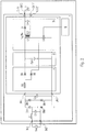
- Figure 2 shows a circuit diagram of a preferred embodiment of the lighting device, the operating device and the converter circuit according to the present invention.
- the lighting device 1 comprises an operating device 2 and a lighting means 7 (represented in Figure 2 by the symbol for a LED), wherein the lighting means 7 are connected to the output terminals OUT2, OUT2' of the operating device 2.
- the lighting means 7 are as described already above.
- the operating device 2 comprises a high potential input terminal IN2 and a low potential input terminal IN2' for supplying an input voltage Vin, such as e.g. mains voltage, to the operating device 2.
- Vin such as e.g. mains voltage
- the operating device 2 comprises a filter circuit, formed by an inductor Lf and a capacitor Cf, and a rectifier circuit, formed by the four diodes DBn, DBr2, DBr3 and DBr4, for filtering and rectifying the input voltage Vin supplied to the input terminals IN2, IN2' of the operating device 2.
- the filter circuit and rectifier circuit of the operating device 2 may also be differently implemented.
- the operating device may also not comprise a filter circuit and a rectifier circuit.
- the input voltage Vin is preferably a DC voltage, such as the voltage of a battery, or a rectified AC voltage, such as a rectified mains voltage.
- the operating device 2 also comprises a converter circuit 3 and a controller 6.
- the input voltage Vin is stored in a capacitor Cin after having been filtered by the inductor Lf and capacitor Cf and having been rectified by the full-bridge rectifier circuit formed by the four diodes DBr1, DBr2, DBr3 and DBr4.
- the capacitor Cin is an electrical energy storage element that provides to the converter circuit 3, in particular to the input terminals IN3, IN3' of the converter circuit 3, a filtered and rectified AC input voltage.
- the converter circuit 3 comprises a boost converter stage 4 and a flyback converter stage 5, which are electrically connected respectively coupled via an electrical energy storage element 8, wherein the boost converter stage 4 is arranged in front of the flyback-converter stage 5.
- the boost converter stage 4 comprises an electrical energy storage element in the form of an inductor LB and two diodes DA, DB.
- One side respectively one terminal of the inductor LB is electrically connected to the high potential input terminal IN3 of the converter circuit 3 and the other side respectively other terminal of the inductor LB is connected to the anode of the diode DA and to the anode of the diode DB.
- the terms “electrically connected”, “connected”, “electrically coupled” and “coupled” are used as synonyms. Furthermore, with respect to describing the connection of electrical elements in the present invention the terms “ a side” of an electrical element and “ a terminal” of an electrical element are used as synonyms. To describe in the present invention the two sides respectively terminals of an electrical element, to which another electrical element is connectable, the terms “ a side / terminal” and “another side / terminal” of an electrical element and "a first side / terminal” and " a second side / terminal” of an electrical element are used as synonyms.
- the cathode of the diode DA is connected to the transformer of the flyback converter stage 5, in particular to a first terminal of the first inductor respectively first winding L1 of the transformer.
- the cathode of the diode DA is also connected to the capacitor Cpfc forming the electrical energy storage element 8, which connects the boost converter stage 4 and the flyback converter 5 stage to each other.
- the cathode of the diode DB is connected to the second terminal of the primary inductor respectively primary winding L1 of the transformer of the flyback converter stage 5 and to a second terminal of the switch S1 of the converter circuit 3, in particular of the flyback converter stage 5.
- the cathode of the diode DA is connected to the node between the transformer, in particular the primary winding L1 of the transformer, and the switch S1.
- the flyback converter stage 5 of the converter circuit 3 comprises a transformer that galvanically isolates a primary side of the flyback converter stage 5 from a secondary side of the flyback converter stage 5.
- the converter circuit 3 also has a primary side galvanically isolated by the transformer of the flyback converter stage 5 from a secondary side of the converter circuit 3.
- the boost converter stage 4 On the primary side of the converter circuit 3 the boost converter stage 4, the electrical energy storage element 8 and the primary side of the flyback converter stage 5 are arranged.
- the secondary side of the flyback converter stage 5 On the secondary side of the converter circuit 3 the secondary side of the flyback converter stage 5 is arranged.
- the primary inductor respectively primary winding L1 of the transformer and the switch S1 of the converter circuit 3 are arranged.
- the primary winding L1 of the transformer is connected in series to the switch S1.
- the first terminal of the primary winding L1 is connected to the cathode of the diode DA of the boost converter stage 4 and the second terminal of the primary winding L1 of the transformer is connected to the second terminal of the switch S1.
- the first terminal of the switch S1 is connected to the low potential input terminal IN3' of the converter circuit 3 and to the capacitor Cpfc that forms the electrical energy storage element 8.
- a diode Do and a capacitor Co are arranged on the secondary side of the flyback converter stage 2 on the secondary side of the flyback converter stage 2 .
- the diode Do is arranged such that a flow of current from the output OUT3, OUT3' of the converter circuit 3 to the primary side of the flyback converter stage 5 is prevented.
- the anode of the diode Do is connected to the secondary winding L2 of the transformer and the cathode of the diode Do is connected to the capacitor Co.
- the capacitor Co is arranged in parallel to the secondary winding L2 of the transformer in order to store the voltage respectively the electrical power transferred via the transformer from the primary side to the secondary side of the flyback converter stage 5.
- the diode Do and the capacitor Co rectify the voltage provided by the secondary winding L2 of the transformer.
- the diode Do and the capacitor Co may also be arranged outside the flyback converter stage, as long as they are connected to the secondary winding L2 of the transformer of the flyback converter stage 5 and rectify the voltage supplied by the secondary winding L2 of the transformer.
- the primary winding L1 of the transformer forms the electrical energy storage element of the flyback converter stage 5.
- the switch S1 of the flyback converter stage 5 forms the switch of the converter circuit 3.
- Figure 2 shows a preferred embodiment of the converter circuit according to the present invention, in which the DC-to-DC converter stage of the converter circuit is a flyback converter stage and in which the DC-to-DC converter stage comprises the switch of the converter circuit for controlling the operation of both the boost converter stage and the DC-to-DC converter stage.
- the switch may also be differently arranged, such that the boost converter stage comprises the switch, and the DC-to-DC converter stage may also be differently implemented.
- the DC-to-DC converter stage may also be a buck converter stage.
- the controller 6 is configured to control the switch S1 in order to control the operation of the boost converter stage 4 and the flyback converter stage 5.
- the controller 6 is configured to cyclically switch the switch S1 in order to cyclically charge and discharge the electrical energy storage element LB of the boost converter stage 4 and the electrical energy storage element L1 of the flyback converter stage 5.
- the controller 6 of the operation circuit 2 is on the same potential as the primary side of the converter circuit 3.
- the switch S1 and the controller 6 may be implemented as already outlined above.
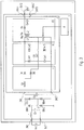
- Figure 3 shows a circuit diagram of another preferred embodiment of the lighting device, the operating device and the converter circuit according to the present invention.
- the preferred embodiment according to Figure 3 basically corresponds to the preferred embodiment according to Figure 2 and, thus, the above description of the preferred embodiment of Figure 2 is also valid for the preferred embodiment of Figure 3 .
- the two preferred embodiments differ in the way the boost converter stage 4 and the flyback converter stage 5 of the converter circuit 3 are connected to each other.
- the boost converter stage 4 and the flyback converter stage 5 of the converter circuit 3 are connected to each other via a electrical energy storage element 8 formed by the capacitor Cpfc.
- the boost converter stage 4 and the flyback converter stage 5 of the converter circuit 3 are connected to each other by a passive power factor correction circuit 9.
- the passive power factor correction circuit is formed by a valley fill circuit comprising two capacitors Cvf1, Cvf2 and three diodes Dvf1, Dvf2, Dvf3.
- the passive power factor correction circuit may also be differently implemented.
- Figure 4 shows an equivalent circuit diagram of the preferred embodiment of the converter circuit according to the present invention shown in Figure 3 .
- the equivalent circuit diagram of Figure 4 basically corresponds to the circuit diagram of the converter circuit shown in Figure 3 .
- the electrical energy storage element L1 of the flyback converter stage is represented in Figure 4 by inductors L_lkg and Lm connected in series, wherein the inductor Lm is connected in parallel to the primary winding of the transformer of the flyback converter stage 5. That is, the inductors L_lkg and Lm and the primary winding of the transformer of the flyback converter stage 5 shown in Figure 4 correspond to the primary inductor respectively primary winding L1 of the transformer of the flyback converter stage 5 shown in Figure 3 .
- the switch S1 is a MOSFET, wherein the output capacitance Coss and the body diode of the MOSFET are indicated.
- the control signals from the controller for switching the switch S1 are supplied to the gate terminal of the MOSFET.
- the switch S1 may also be differently implemented.
- the diode Do and the capacitor Co which rectify the voltage provided by the secondary winding L2 of the transformer of the flyback converter stage 5, are not part of the flyback converter stage 5.
- the shunt resistor Rsns is a current sensing element which is connected to the primary side of the flyback converter stage 5 of the converter circuit 3 in order to sense the current flowing through the boost converter stage 4 and the current flowing through the DC-to-DC converter stage 5, when the switch S1 is in the conducting stage.
- the shunt resistor Rsns is arranged on a potential not linked to ground it may be advantageous to sense the voltage over shunt resistor Rsns by the aid of a level shifter or optocoupler. It would be also possible to sense the voltage difference over the shunt resistor Rsns in order to measure the current flowing through the shunt resistor Rsns.
- the load at the output of the converter circuit 3 is indicated in Figure 4 by a resistor Ro.
- the equivalent circuit shown in Figure 4 is merely for explaining the operation of the converter circuit according to the present invention by way of example, when the switch S1 of the converter circuit 3 is controlled in the discontinuous conduction mode (cf. Figures 5a to 5e below).
- Figures 5a to 5e show equivalent circuit diagrams of the preferred embodiment of the converter circuit according to Figure 3 for different phases of a preferred embodiment of a discontinuous conduction mode control.
- Figure 5a shows the equivalent circuit diagram of the preferred embodiment of the converter circuit according to Figure 3 for a first phase of a control cycle of a preferred embodiment of the discontinuous conduction mode.
- the switch S1 In the first phase the switch S1 is in the conducting state.
- the diode DA of the boost converter stage 4 is blocked respectively reverse biased and the diode DB of the boost converter stage 4 is conducting. No electrical energy is transferred from the primary side to the secondary side of the flyback converter stage 5 via the transformer.
- the load Ro is supplied with electrical energy stored in the capacitor Co of the secondary side of the flyback converter stage 5.
- the first phase of a control cycle of the discontinuous conduction mode corresponds to the time period between the time T0 and T1 shown in Figure 6 .
- the switch S1 being in the conducting state during the first phase the current ILB flowing through the electrical energy storage element LB of the boost converter stage 4 rises and the electrical energy storage element LB is charged (cf. graph "iLB" of Figure 6 ).
- the electrical energy storage element L1 of the flyback converter stage 5 is also charged with electrical energy stored in the capacitors Cvfi and Cvf2 of the valley fill circuit 9 and the current IPri flowing through the electrical energy storage element L1 of the flyback converter rises (cf. graph "ipri" of Figure 6 ). Both the current ILB of the electrical energy storage element LB and the current IPri of the electrical energy storage element L1 flow through the switch S1 in the first phase.
- Figure 5b shows the equivalent circuit diagram of the preferred embodiment of the converter circuit according to Figure 3 for a second phase of a control cycle of a preferred embodiment of the discontinuous conduction mode.
- the switch S1 is switched to the non-conducting state.
- the diode DA of the boost converter stage 4 starts conducting while the diode DB of the boost converter stage is still conducting.
- No electrical energy is transferred from the primary side to the secondary side of the flyback converter stage 5 via the transformer.
- the load Ro is supplied with electrical energy stored in the capacitor Co of the secondary side of the flyback converter stage 5.
- the second phase of a control cycle of the discontinuous conduction mode corresponds to the time period between the time T1 and T2 shown in Figure 6 .
- Both the electrical energy storage element LB of the boost converter stage 4 and the electrical energy storage element L1 of the flyback converter stage 5 start to discharge and, thus, the current ILB of the electrical energy storage element LB and the current IPri of the electrical energy storage element L1 start to fall (cf. graphs "iLB” and "ipri" of Figure 6 ).
- Figure 5c shows the equivalent circuit diagram of the preferred embodiment of the converter circuit according to Figure 3 for a third phase of a control cycle of a preferred embodiment of the discontinuous conduction mode.
- the switch S1 In the third phase the switch S1 is still in the non-conducting state. Electrical energy is transferred from the boost converter stage 4 to the capacitors Cvfi and Cvf2 of the valley fill circuit 9 and electrical energy is transferred from the primary side to the secondary side of the flyback converter stage 5 via the transformer.
- the third phase of a control cycle of the discontinuous conduction mode corresponds to the time period between the time T2 and T3 shown in Figure 6 .
- Both the electrical energy storage element LB of the boost converter stage 4 and the electrical energy storage element L1 are still being discharged and, thus, the current ILB of the electrical energy storage element LB and the current IPri of the electrical energy storage element L1 continue to fall (cf. graphs " iLB " and "ipri" of Figure 6 ).
- the leakage electrical energy of the flyback converter circuit has dissipated, i.e. the inductor L_lkg representing in Figures 5a to 5e the leakage energy is completely discharged.
- Figure 5d shows the equivalent circuit diagram of the preferred embodiment of the converter circuit according to Figure 3 for a fourth phase of a control cycle of a preferred embodiment of the discontinuous conduction mode.
- the switch S1 is still in the non-conducting state.
- the boost converter stage 4 is no longer transferring electrical energy to the capacitors Cvfi and Cvf2 of the valley fill circuit 9.
- the flyback converter stage 5 is still transferring electrical energy from its primary side to its secondary side via the transformer.
- the fourth phase of a control cycle of the discontinuous conduction mode corresponds to the time period between the time T3 and T4 shown in Figure 6 .
- the electrical energy storage element LB of the boost converter stage 4 is completely discharged. That is, the current ILB of the electrical energy storage element LB has reached zero amperes (cf. graph "iLB" of Figure 6 ).
- the boost converter stage 4 reaches at the beginning of the fourth phase the non-conducting phase.
- the electrical energy storage element LB of the boost converter stage 4 is kept uncharged during the fourth phase.
- the electrical energy storage element L1 is still being discharged and, thus, the current IPri of the electrical energy storage element L1 continues to fall (cf.
- Figure 5e shows the equivalent circuit diagram of the preferred embodiment of the converter circuit according to Figure 3 for a fifth phase of a control cycle of a preferred embodiment of the discontinuous conduction mode.
- the switch S1 is still in the non-conducting state.
- the boost converter stage 4 is still not transferring electrical energy to the capacitors Cvfi and Cvf2 of the valley fill circuit 9 and the flyback converter stage 5 is not transferring anymore electrical energy from its primary side to its secondary side via the transformer.
- the conductor Co on the secondary side of the flyback converter stage 5 supplies the load Ro with electrical energy.
- the fifth phase of a control cycle of the discontinuous conduction mode corresponds to the time period between the time T4 and T0 shown in Figure 6 .
- the boost converter stage 4 is kept in the non-conducting stage during the fifth phase.
- the electrical energy storage element LB of the boost converter stage 4 is kept uncharged during the fifth phase.
- the electrical energy storage element L1 of the flyback converter stage 5 is completely discharged. That is, the current Ipri of the electrical energy storage element L1 has reached zero amperes (cf. graph "ipri" of Figure 6 ).
- the flyback converter stage 5 reaches at the beginning of the fifth phase the non-conducting phase. (cf. graph "ipri" of Figure 6 ). Therefore, in the fifth phase the flyback converter stage 5 reaches the non-conducting phase after the boost converter stage 4 has already reached the non-conducting phase in the fourth phase (cf. graphs "iLB" and "ipri" of Figure 6 ).
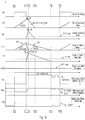
- Figure 6 shows electrical parameters of the preferred embodiment of the converter circuit according to Figure 3 for the different phases of the preferred embodiment of a discontinuous conduction mode control shown in Figures 5a to 5e .
- the first phase of a control cycle of the discontinuous conduction mode corresponds to the time period between the time T0 and T1 of Figure 6 ;
- the second phase of the control cycle (shown in Figure 5b ) corresponds to the time period between the time T1 and T2 of Figure 6 ;
- the third phase of the control cycle (shown in Figure 5c ) corresponds to the time period between the time T2 and T3 of Figure 6 ;
- the fourth phase of the control cycle (shown in Figure 5d ) corresponds to the time period between the time T3 and T4 of Figure 6 and the fifth phase of the control cycle (shown in Figure 5e ) corresponds to the time period between the time T4 and T0 of Figure 6 .
- the graph "GD" of Figure 6 shows the control signal applied to the gate-terminal of the switch S1 for controlling the switching of the switch S1 over time. During a high signal the switch S1 is in the conducting state and during a low signal the switch S1 is in the non-conducting state.
- the graph " iLB” of Figure 6 shows the current flow over time of the current ILB flowing through the electrical energy storage element LB of the boost converter stage 4.
- the graph "iDA" of Figure 6 shows the current flow over time of the current IDA flowing through the diode DA of the boost converter stage 4.
- the graph “ipri” of Figure 6 shows the current flow over time of the current IPri flowing through the electrical energy storage element L1 of the flyback converter stage 5.
- the current flow over time of the current iLkg flowing through the inductor L_lkg and of the current iLm flowing through the inductor Lm are also indicated.
- the inductors L_lkg and Lm are part of the electrical energy storage element L1 of the flyback converter stage 5 in the equivalent circuit diagram of Figures 5a to 5e .
- the graph " iDo" of Figure 6 shows the current flow over time of the current IDo flowing through the diode Do on the secondary side of the flyback converter stage 5.
- Vcf1 / 2 shows the average voltage Vcf1_avg of the capacitor Cvfi of the valley fill circuit 9 over time.
- the graph "Vds" of Figure 6 shows the drain-source-voltage Vds across the MOSFET forming the switch S1 of the flyback converter stage 5 over time.
- Vlink of Figure 6 shows the voltage seen across the capacitors Cvfi and Cvf2 of the valley fill circuit 9 over time.
- the graph " VDO" of Figure 6 shows the voltage across the diode Do on the secondary side of the flyback converter stage 5 over time.
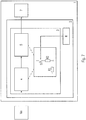
- Figure 7 shows the conceptual block diagram of Figure 1 , schematically indicating a preferred embodiment of sensing current according to the present invention. The above description of Figure 1 is also valid for Figure 7 .
- the converter circuit 3 further comprises two shunt resistors R1, R2 as current sensing elements which are connected to the switch S1 of the converter circuit 3 in order to sense the current flowing through the boost converter stage 4 and the current flowing through the DC-to-DC converter stage 5, when the switch S1 is in the conducting stage.
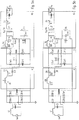
- Figure 8 shows the circuit diagram of the preferred embodiment of the converter circuit according to the present invention shown in Figure 2 with a preferred embodiment of sensing current according to the present invention.
- the current sensing according to the present invention may be also implemented with a converter circuit 3 having a passive power factor correction circuit 9, such as a valley fill circuit, for coupling the boost converter stage 4 and the DC-to-DC converter stage 5 and/or having a different type of DC-to-DC converter stage 5 compared to the flyback converter stage of Figure 8 .
- a passive power factor correction circuit 9 such as a valley fill circuit
- the converter circuit 3 also comprises two current sensing elements in the form of two shunt resistors R1 and R2 for sensing the current flowing through the boost converter stage 4 and the current flowing through the flyback converter stage 5.
- the two shunt resistors R1 and R2 are configured to sense together the current flowing through the inductor LB of the boost converter stage 4 and the current flowing through the primary winding L1 of the transformer of the flyback converter stage 5.
- the shunt resistor R1 is connected between a first node n1 and a second node n2 of the converter circuit 3.
- the first node n1 corresponds to the low potential input terminal IN3' of the converter circuit 3.
- the shunt resistor R2 is connected to the first terminal of the switch S1 and the second node n2 of the converter circuit 3.
- the node between the first terminal of the switch S1 and the shunt resistor R2 is referred to as the third node n3.
- the capacitor Cpfc forming the electrical energy storage element 8 is also connected on one side to the second node n2.
- the current of the boost converter stage 4 and the current of the flyback converter stage 5 flow through the conducting switch S1 and, thus, are sensed by the resistor R2.
- the current of the boost converter stage 4 in particular of the inductor LB, flows via the diode DB and the switch S1 to the shunt resistor R2, while the diode DA is reverse biased, when the switch S1 is in the conducting state.
- All the current that flows through the primary winding L1 of the transformer of the flyback converter stage 5 is sourced from the capacitor Cpfc and flows via the switch S1 to the shunt resistor R2, when the switch S1 is conducting.
- both the current of the boost converter stage 4 and the current of the flyback converter stage 5 flow through the shunt resistor R2, when the switch S1 is in the conducting state.
- the sensing result of the shunt resistor R2 is the sum of the current of the boost converter stage 4 and the current of the flyback converter stage 5 and the sensing result of the shunt resistor R1 is only the current of the boost converter stage 4.
- the sensing results of the shunt resistor R1 and the shunt resistor R2 are feed to the controller 6 (not shown in Figure 8 ).
- the controller 6 may then determine on the basis of these sensing results the current of the flyback converter stage 5 and, thus, may control the switch S1 on the basis of the current of the flyback converter stage 5.
- the shunt resistors R1 and R2 have the same resistance value.
- the shunt resistors R1 and R2 of the embodiment of Figure 8 offer the advantage of measurements on shunt resistors linked to ground where no level shifter or opto-coupler is necessary to sense the signals at the measurement points. Such arrangement would provide less complicated measurement in comparison to the embodiment of Figure 4 where the shunt resistor Rsns is arranged on a position not directly inked to ground.
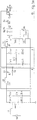
- Figure 9 shows the equivalent circuit diagram of the preferred embodiment of the converter circuit according to the present invention shown in Figure 2 with a preferred embodiment of sensing current according to the present invention.
- the preferred embodiment of sensing current according to Figure 9 basically corresponds to the preferred embodiment of sensing current according to Figure 8 and, thus, the above description of the preferred embodiment of Figure 8 is also valid for the preferred embodiment of Figure 9 .
- the above description of Figure 2 is also valid for Figure 9 .
- the embodiment according to Figure 9 differs from the embodiment according to Figure 8 in that the converter circuit 3 according to Figure 9 comprises two additional current sensing elements in the form of two addition shunt resistors R3 and R4.
- the two additional shunt resistors R3 and R4 are provided in the converter circuit 3 for feeding the sensing results of the shunt resistors R1 and R2 to the controller 6 of the operating device 2.
- the shunt resistor R4 is connected on one side to the first node n1 of the converter circuit 3 and the shunt resistor R3 is connected on one side to the third node n3 between the switch S1 and the shunt resistor R2 of the converter circuit 3.
- the other side of the shunt resistor R4 and the other side of the shunt resistor R3 are connected to each other and to the controller 6.
Landscapes
- Engineering & Computer Science (AREA)
- Power Engineering (AREA)
- Circuit Arrangement For Electric Light Sources In General (AREA)
- Dc-Dc Converters (AREA)
Abstract
Description
- The present invention relates to a converter circuit, an operating device for lighting means with such a converter circuit, as well as a lighting device with such an operating device and lighting means. In addition, a method for controlling a converter circuit according to the present invention is proposed.
- In the prior art actively switched converter circuits for converting an input voltage to an output voltage in order to provide an operating voltage, operating current or operating power for lighting means, such as a LED, are well known.
- Ensuring on one side a high power factor (PF) and total harmonic distortion (THD) for such a converter circuit and on the other side reducing the costs for such a converter circuit as well as reducing the complexity of controlling the switch of such an actively switched converter circuit constitutes a common problem in the state of the art.
- In addition, the sensing of a current in such a converter circuit without great effort constitutes a further problem in the state of the art.
- Therefore, it is an object of the present invention to provide a converter circuit for converting an input voltage into an output voltage, which has a high power factor and total harmonic distortion, reduces the costs and the complexity of controlling the converter circuit as well as provides means for sensing a current in the converter circuit without great effort. In addition, it is an object of the present invention to provide an operating device for lighting means comprising such a converter circuit as well as to provide a lighting device with such an operating device and lighting means.
- These and other objects, which become apparent upon reading the following description, are solved by the subject-matter of the independent claims. The dependent claims refer to preferred embodiments of the invention.
- According to the present invention a converter circuit for converting an input voltage into an output voltage is provided, wherein the converter circuit comprises an actively switched boost converter stage with a first electrical energy storage element, an actively switched DC-to-DC converter stage with a second electrical energy storage element, a switch controllable by a controller for operating both the actively switched boost converter stage and the actively switched DC-to-DC converter stage, a first current sensing element, and a second current sensing element; wherein the first current sensing element and the second current sensing element are configured to sense the current of the first electrical energy storage element and the current of the second electrical energy storage element with respect to the low potential of the converter circuit, preferably with respect to ground potential, when the switch is in the conducting state.
- That is, the present invention provides a converter circuit with an actively switched boost converter stage, an actively switched DC-to-DC converter stage and one switch, wherein the voltage conversion by the actively switched boost converter stage and the voltage conversion by the actively switched DC-to-DC converter stage is controllable by switching the one switch. Furthermore, the converter circuit comprises a first current sensing element and a second current sensing element that are arranged in the converter circuit such that they are configured to sense with respect to the low potential of the converter circuit, preferably with respect to ground potential, the current flowing through the boost converter stage, in particular through the first electrical energy storage element of the boost converter stage, and the current flowing through the DC-to-DC converter stage, in particular through the second electrical energy storage element of the DC-to-DC converter stage, when the switch is in the conducting stage.
- Sensing current with respect to the low potential of the converter circuit, preferably with respect to ground potential, has a benefit over sensing current with respect to a variable potential, as the external circuitry for evaluating the sensing result is simplified.
- Moreover, the control of two converter stages is achieved by only one switch used for actively switching the two converter stages and, thus, for controlling the voltage conversion by each of the two converter stages. As a result, the number of electronic components can be reduced, saving costs, and the complexity of control for the converter circuit is reduced.
- The converter circuit is a circuit that is configured to convert an input voltage respectively input power into a higher or lower output voltage respectively output power by preferably cyclically switching the switch of the converter circuit.
- An "actively switched boost converter stage" according to the present invention is a boost converter circuit respectively step-up converter circuit that is configured to convert an DC input voltage or rectified AC input voltage into a higher DC output voltage via preferably cyclically charging and discharging an electrical energy storage element, such as an inductor. The preferably cyclically charging and discharging of the electrical energy storage element is controlled by preferably cyclically switching a switch.
- In the following the terms "actively switched boost converter stage" and "boost converter" are used as synonyms.
- An "actively switched DC-to-DC converter stage" according to the present invention is a DC-to-DC converter circuit that is configured to convert an DC input voltage or rectified AC input voltage into a lower or higher DC output voltage via preferably cyclically charging and discharging an electrical energy storage element, such as an inductor. The preferably cyclically charging and discharging of the electrical energy storage element is controlled by preferably cyclically switching a switch. The boost convert circuit is one specific type of DC-to-DC converter circuit.
- In the following the terms "actively switched DC-to-DC converter stage" and "DC-to-DC converter stage" are used as synonyms.
- Preferably, the input voltage is a DC voltage, such as the voltage supplied by a battery, or a rectified AC voltage, such as a rectified mains voltage.
- Preferably, the switch is a transistor, more preferably a MOSFET or a bipolar transistor.
- Preferably, the first electrical energy storage element and the second electrical energy storage element are an inductor.
- In case, the DC-to-DC converter stage is a DC-to-DC converter circuit with a transformer for galvanic isolation between the input and output, such as a flyback converter circuit, the second electrical energy storage element is preferably the primary winding of the transformer used for the galvanic isolation.
- Preferably, the first current sensing element and the second current sensing element are shunt resistors, which preferably have the same resistance value.
- Preferably, the input of the DC-to-DC converter stage is electrically connected in series to the output of the boost converter stage.
- With other words, the boost converter stage and the DC-to-DC converter stage are preferably cascaded, such that the boost converter stage is followed by the DC-to-DC converter stage.
- The boost converter stage and the DC-to-DC converter stage preferably form the voltage conversion line respectively power conversion line of the converter circuit, such that the boost converter stage is followed by the DC-to-DC converter stage in the voltage conversion line respectively power conversion line.
- Preferably, the first current sensing element is electrically connected between a first node and a second node of the converter circuit; the second current sensing element is electrically connected to a first terminal of the switch and the second node of the converter circuit, such that the second current sensing element is electrically connected between the switch and the second node; and the low potential input terminal of the converter circuit is electrically connected to the first node.
- In this regard it is noted that the switch has a first terminal and a second terminal, to which an electrical element may be connected, respectively, such that an electrical path is formed between the electrical element connected to the first terminal and the electrical element connected to the second terminal when the switch is in the conducting state.
- The passage "the low potential input terminal of the converter circuit is electrically connected to the first node" means that the low potential input terminal corresponds to the first node, i.e. the low potential input terminal of the converter circuit and the first node of the converter circuit are on the same potential.
- Preferably, the second electrical energy storage element is electrically connected to a second terminal of the switch, such that the switch is electrically connected between the second electrical energy storage element and the second current sensing element; and the first electrical energy storage element is electrically connected via a diode to the second terminal of the switch, such that the anode of the diode is electrically connected to the first electrical energy storage element and the cathode of the diode is electrically connected to the second terminal of the switch.
- Preferably, the converter circuit comprises a third and fourth current sensing element; wherein the third current sensing element is electrically connected on one side with the node between the first terminal of the switch and the second current sensing element; and wherein the fourth current sensing element is electrically connected on one side with the first node of the converter circuit.
- Preferably, the other side of the third current sensing element and the other side of the fourth current sensing element are electrically connected to each other.
- Preferably, the third current sensing element and the fourth current sensing element are shunt resistors, which preferably have the same resistance value.
- Preferably, the boost converter stage and the DC-to-DC-converter stage are electrically connected to each other via a third electrical energy storage element or via a passive power factor correction circuit, wherein preferably the passive power factor correction circuit is a valley fill circuit.
- The third electrical energy storage element is preferably a capacitor. This has the benefit that the boost converter stage and the DC-to-DC converter stage may be coupled to each other in a cost effective way.
- A passive power factor correction circuit, such as a valley fill circuit, for coupling the boost converter stage and the DC-to-DC converter stage with each other has the benefit, that the power factor (PF) and the total harmonic distortion (THD) of the converter circuit is improved.
- Preferably, the DC-to-DC converter stage is a flyback converter stage or a buck converter stage.
- That is, preferably, the DC-to-DC converter stage is a flyback converter circuit with a transformer for galvanic isolation between the input and output or a buck converter circuit.
- Preferably, in case the DC-to-DC converter stage is a flyback converter stage and comprises the switch, the flyback converter stage is a primary side control flyback converter circuit, i.e. the switch is arranged on the primary side of the flyback converter stage with respect to the galvanic isolation.
- Preferably, the DC-to-DC converter stage comprises the switch or the boost converter stage comprises the switch.
- According to the present invention an operating device for operating lighting means is also provided, wherein the operating device comprises input terminals for supplying an input voltage to the operating device, output terminals for electrically connecting the lighting means to the operating device, and a converter circuit according to the present invention, as outlined above; wherein the converter circuit is configured to convert the input voltage supplied to the operating device to an operating voltage for operating the lighting means and to supply the operating voltage to the output terminals of the operating device.
- In other words, the operating device is configured to operate lighting means, in that the converter circuit of the operating device is configured to convert an input voltage into an output voltage. As a result thereof, the operating device is able to provide at its output terminals an operating voltage, operating current or operating power for the operation of the lighting means.
- Preferably, the operating device is a low power LED operating device respectively low power LED driver, such as e.g. an emergency operating driver or maintained mode driver for LEDs.
- Preferably, the operating device comprises a controller, wherein the controller is configured to control the switching of the switch of the converter circuit.
- That is, preferably, the controller of the operating device is configured to preferably cyclically switch the switch of the converter circuit in order to control the operation of the boost converter stage and the DC-to-DC converter stage.
- Preferably, the controller is a microcontroller, an application-specific integrated circuit (ASIC) or a hybrid thereof.
- Preferably, the controller is configured to control the switching of the switch of the converter circuit based on the current of the second electrical energy storage element.
- With other words, preferably, the controller is configured to control the switch on the basis of the current flowing through the second electrical energy storage element of the DC-to-DC converter stage, which current is sensed by the first and second current sensing element.
- Preferably, the controller is configured to obtain via the third current sensing element and the fourth current sensing element the current of the second electrical energy storage element.
- According to the present invention an lighting device is also provided, wherein the lighting device comprises an operating device according to the present invention, as outlined above, and lighting means electrically connected to the output terminals of the operating device; wherein the operating device is configured to supply the lighting means with electrical energy.
- That is, the operating device is configured to operate the lighting means by providing an operating voltage, operating current and/or operating power.
- Preferably, the lighting means comprises at least one light source, such as a LED, a luminescent lamp or any other light source configured to transmit light.
- More preferably, the lighting means comprises at least one LED. In case the lighting means comprises more than one LED, the LEDs of the lighting means are preferably electrical connected to each other in series and/or parallel.
- The term "LED" is to be understood as comprising any type of light-emitting diode, such as organic LED, non-organic LED, low power LED, high power LED, etc.
- According to a preferred embodiment, the operating device of the lighting device is a low power LED operating device respectively low power LED driver, such as e.g. an emergency operating driver or maintained mode driver for LEDs, and, preferably, the lighting means of the lighting device comprises at least one low power LED, such as e.g. an emergency LED for providing an emergency lighting.
- The previous optional features may be combined in any way to form the method for controlling the converter circuit according to the present invention.
- In the following, preferred embodiments of the present invention are described exemplarily with reference to the enclosed figures, in which
- Figure 1
- shows a conceptual block diagram of a preferred embodiment of the lighting device, the operating device and the converter circuit according to the present invention.
- Figure 2
- shows a circuit diagram of a preferred embodiment of the lighting device, the operating device and the converter circuit according to the present invention.
- Figure 3
- shows a circuit diagram of another preferred embodiment of the lighting device, the operating device and the converter circuit according to the present invention;
- Figure 4
- shows an equivalent circuit diagram of the preferred embodiment of the converter circuit according to the present invention shown in
Figure 3 ; - Figures 5a to 5e
- show equivalent circuit diagrams of the preferred embodiment of the converter circuit according to
Figure 3 for different phases of a preferred embodiment of a discontinuous conduction mode control; - Figure 6
- shows electrical parameters of the preferred embodiment of the converter circuit according to
Figure 3 for the different phases of the preferred embodiment of a discontinuous conduction mode control shown inFigures 5a to 5e ; - Figure 7
- shows the conceptual block diagram of
Figure 1 , schematically indicating a preferred embodiment of sensing current according to the present invention; - Figure 8
- shows the circuit diagram of the preferred embodiment of the converter circuit according to the present invention shown in
Figure 2 with a preferred embodiment of sensing current according to the present invention; - Figure 9
- shows the equivalent circuit diagram of the preferred embodiment of the converter circuit according to the present invention shown in
Figure 2 with a preferred embodiment of sensing current according to the present invention. - In the
figures 1 to 9 corresponding features and electrical parameters are referenced by the same reference signs. -
Figure 1 shows a conceptual block diagram of a preferred embodiment of the lighting device, the operating device and the converter circuit according to the present invention. - According to
Figure 1 thelighting device 1 comprises anoperating device 2 and lighting means 7. - As outlined already above, the lighting means 7 preferably comprises at least one light source, such as a LED, a luminescent lamp or any other light source configured to transmit light.
- More preferably, the lighting means comprises at least one LED. In case the lighting means comprises more than one LED, the LEDs of the lighting means are preferably electrical connected to each other in series and/or parallel.
- The operating
device 2 ofFigure 1 comprises aconverter circuit 3 and acontroller 6. - The
converter circuit 3 comprises an actively switched boost converter stage 4 (in the following referred to as "boost converter stage"), an actively switched DC-to-DC converter stage 5 (in the following referred to as "DC-to-DC converter stage") and a switch S1. As indicated by the dashed lines the operation of both theboost converter stage 4 and the DC-to-DC converter stage 5 is controlled by the one switch S1 of theconverter circuit 3. - Each of the
boost converter stage 4 and the DC-to-DC converter stage 5 is configured to convert an input voltage into an output voltage by preferably cyclically charging and discharging a respective electrical energy storage element, such as an inductor. Thereby, the charging and discharging of the respective electrical energy storage element and, thus, the voltage conversion is controlled by the switching of the switch S1. - As outlined already above, preferably, the DC-to-DC converter stage is a buck converter stage or a flyback converter stage.
- As shown in
Figure 1 theboost converter stage 4 and the DC-to-DC converter stage 5 form the voltage conversion line respectively power conversion line of theconverter circuit 3, in which theboost converter stage 4 is arranged in front of the DC-to-DC converter stage 5. That is, theboost converter stage 4 and the DC-to-DC converter stage are cascaded to form the voltage conversion line respectively power conversion line of theconverter circuit 3. Thus, theboost converter stage 4 and the DC-to-DC converter stage 5 are connected in series to each other. The arrows indicate the voltage path through the voltage conversion line formed by theboost converter stage 4 and the DC-to-DC converter stage 5 of theconverter circuit 3. - The
converter circuit 3 is configured to convert a DC input voltage Vin or an rectified AC input voltage Vin into an output voltage in order to provide an operating voltage, operating current or operating power for the lighting means 7. - The
controller 6 of theoperating device 2 is preferably a microcontroller, application-specific integrated circuit (ASIC) or a hybrid thereof, that is configured to control the switching of the switch S1 of theconverter circuit 3. Preferably, thecontroller 6 is configured to control the switch such that theconverter circuit 3, in particular theboost converter stage 4 and the DC-to-Dc converter stage 5, are operated in the discontinuous conduction mode. The arrow from thecontroller 6 to the switch S1 indicates inFigure 1 that the controller is configured to control the switch and, thus, is configured to control the operation of theconverter circuit 3, in particular the operation of theboost converter stage 4 and the DC-to-DC converter stage 5. - In
Figure 1 there is no indication that the controller receives any sensed or measured electrical parameters from theconverter circuit 3 or the lighting means 7, for controlling the switch S1 in order to control the operating voltage, operating current or operating power supplied by the operatingdevice 2 to the lighting means 7. Nevertheless, theboost converter stage 4, the DC-to-DC converter stage 5, theconverter circuit 3, the operatingdevice 2, the lighting means 7 and/or thelighting device 1 may be configured such that thecontroller 6 is able to perform a feed-back control of the switch S1 on the basis of one or more electric parameters from any of the elements mentioned before. -
Figure 2 shows a circuit diagram of a preferred embodiment of the lighting device, the operating device and the converter circuit according to the present invention. - The
lighting device 1 comprises anoperating device 2 and a lighting means 7 (represented inFigure 2 by the symbol for a LED), wherein the lighting means 7 are connected to the output terminals OUT2, OUT2' of theoperating device 2. - The lighting means 7 are as described already above.
- The operating
device 2 comprises a high potential input terminal IN2 and a low potential input terminal IN2' for supplying an input voltage Vin, such as e.g. mains voltage, to theoperating device 2. - Preferably, the operating
device 2 comprises a filter circuit, formed by an inductor Lf and a capacitor Cf, and a rectifier circuit, formed by the four diodes DBn, DBr2, DBr3 and DBr4, for filtering and rectifying the input voltage Vin supplied to the input terminals IN2, IN2' of theoperating device 2. The filter circuit and rectifier circuit of theoperating device 2 may also be differently implemented. Furthermore, the operating device may also not comprise a filter circuit and a rectifier circuit. In this case the input voltage Vin is preferably a DC voltage, such as the voltage of a battery, or a rectified AC voltage, such as a rectified mains voltage. - The operating
device 2 also comprises aconverter circuit 3 and acontroller 6. - As shown in
Figure 2 , the input voltage Vin is stored in a capacitor Cin after having been filtered by the inductor Lf and capacitor Cf and having been rectified by the full-bridge rectifier circuit formed by the four diodes DBr1, DBr2, DBr3 and DBr4. Thus, in case the input voltage Vin is mains voltage, the capacitor Cin is an electrical energy storage element that provides to theconverter circuit 3, in particular to the input terminals IN3, IN3' of theconverter circuit 3, a filtered and rectified AC input voltage. - The
converter circuit 3 according toFigure 2 comprises aboost converter stage 4 and aflyback converter stage 5, which are electrically connected respectively coupled via an electricalenergy storage element 8, wherein theboost converter stage 4 is arranged in front of the flyback-converter stage 5. - The
boost converter stage 4 comprises an electrical energy storage element in the form of an inductor LB and two diodes DA, DB. One side respectively one terminal of the inductor LB is electrically connected to the high potential input terminal IN3 of theconverter circuit 3 and the other side respectively other terminal of the inductor LB is connected to the anode of the diode DA and to the anode of the diode DB. - In the present invention the terms "electrically connected", "connected", "electrically coupled" and "coupled" are used as synonyms. Furthermore, with respect to describing the connection of electrical elements in the present invention the terms "a side" of an electrical element and "a terminal" of an electrical element are used as synonyms. To describe in the present invention the two sides respectively terminals of an electrical element, to which another electrical element is connectable, the terms "a side/terminal" and "another side/terminal" of an electrical element and "a first side/terminal" and "a second side/terminal" of an electrical element are used as synonyms.
- The cathode of the diode DA is connected to the transformer of the
flyback converter stage 5, in particular to a first terminal of the first inductor respectively first winding L1 of the transformer. The cathode of the diode DA is also connected to the capacitor Cpfc forming the electricalenergy storage element 8, which connects theboost converter stage 4 and theflyback converter 5 stage to each other. The cathode of the diode DB is connected to the second terminal of the primary inductor respectively primary winding L1 of the transformer of theflyback converter stage 5 and to a second terminal of the switch S1 of theconverter circuit 3, in particular of theflyback converter stage 5. Thus, the cathode of the diode DA is connected to the node between the transformer, in particular the primary winding L1 of the transformer, and the switch S1. - The
flyback converter stage 5 of theconverter circuit 3 comprises a transformer that galvanically isolates a primary side of theflyback converter stage 5 from a secondary side of theflyback converter stage 5. - Thus, the
converter circuit 3 also has a primary side galvanically isolated by the transformer of theflyback converter stage 5 from a secondary side of theconverter circuit 3. On the primary side of theconverter circuit 3 theboost converter stage 4, the electricalenergy storage element 8 and the primary side of theflyback converter stage 5 are arranged. On the secondary side of theconverter circuit 3 the secondary side of theflyback converter stage 5 is arranged. - On the primary side of the
flyback converter stage 5 the primary inductor respectively primary winding L1 of the transformer and the switch S1 of theconverter circuit 3 are arranged. The primary winding L1 of the transformer is connected in series to the switch S1. In particular, the first terminal of the primary winding L1 is connected to the cathode of the diode DA of theboost converter stage 4 and the second terminal of the primary winding L1 of the transformer is connected to the second terminal of the switch S1. The first terminal of the switch S1 is connected to the low potential input terminal IN3' of theconverter circuit 3 and to the capacitor Cpfc that forms the electricalenergy storage element 8. - On the secondary side of the
flyback converter stage 2 the secondary inductor respectively secondary winding L2 of the transformer, a diode Do and a capacitor Co are arranged. The diode Do is arranged such that a flow of current from the output OUT3, OUT3' of theconverter circuit 3 to the primary side of theflyback converter stage 5 is prevented. In particular, the anode of the diode Do is connected to the secondary winding L2 of the transformer and the cathode of the diode Do is connected to the capacitor Co. The capacitor Co is arranged in parallel to the secondary winding L2 of the transformer in order to store the voltage respectively the electrical power transferred via the transformer from the primary side to the secondary side of theflyback converter stage 5. The diode Do and the capacitor Co rectify the voltage provided by the secondary winding L2 of the transformer. - The diode Do and the capacitor Co may also be arranged outside the flyback converter stage, as long as they are connected to the secondary winding L2 of the transformer of the
flyback converter stage 5 and rectify the voltage supplied by the secondary winding L2 of the transformer. - The primary winding L1 of the transformer forms the electrical energy storage element of the
flyback converter stage 5. The switch S1 of theflyback converter stage 5 forms the switch of theconverter circuit 3. - That is,
Figure 2 shows a preferred embodiment of the converter circuit according to the present invention, in which the DC-to-DC converter stage of the converter circuit is a flyback converter stage and in which the DC-to-DC converter stage comprises the switch of the converter circuit for controlling the operation of both the boost converter stage and the DC-to-DC converter stage. - As outlined above, the switch may also be differently arranged, such that the boost converter stage comprises the switch, and the DC-to-DC converter stage may also be differently implemented. For example, the DC-to-DC converter stage may also be a buck converter stage.
- As indicated in
Figure 2 by the arrow between thecontroller 6 of theoperating device 2 and the switch S1 of theconverter circuit 3, thecontroller 6 is configured to control the switch S1 in order to control the operation of theboost converter stage 4 and theflyback converter stage 5. In particular, thecontroller 6 is configured to cyclically switch the switch S1 in order to cyclically charge and discharge the electrical energy storage element LB of theboost converter stage 4 and the electrical energy storage element L1 of theflyback converter stage 5. By cyclically charging and discharging the electrical energy storage element LB of theboost converter stage 4 and the electrical energy storage element L1 of theflyback converter stage 5 the input voltage respectively electrical power supplied to theconverter circuit 3 is converted to an output voltage respectively electrical power. The value of the voltage respectively electrical power output by theconverter circuit 3 depends on the switching of the switch S1. - Preferably, the
controller 6 of theoperation circuit 2 is on the same potential as the primary side of theconverter circuit 3. - The switch S1 and the
controller 6 may be implemented as already outlined above. -
Figure 3 shows a circuit diagram of another preferred embodiment of the lighting device, the operating device and the converter circuit according to the present invention. The preferred embodiment according toFigure 3 basically corresponds to the preferred embodiment according toFigure 2 and, thus, the above description of the preferred embodiment ofFigure 2 is also valid for the preferred embodiment ofFigure 3 . - The two preferred embodiments differ in the way the
boost converter stage 4 and theflyback converter stage 5 of theconverter circuit 3 are connected to each other. According to the preferred embodiment ofFigure 2 theboost converter stage 4 and theflyback converter stage 5 of theconverter circuit 3 are connected to each other via a electricalenergy storage element 8 formed by the capacitor Cpfc. - In contrast thereto, according to the preferred embodiment of
Figure 3 theboost converter stage 4 and theflyback converter stage 5 of theconverter circuit 3 are connected to each other by a passive powerfactor correction circuit 9. According toFigure 3 the passive power factor correction circuit is formed by a valley fill circuit comprising two capacitors Cvf1, Cvf2 and three diodes Dvf1, Dvf2, Dvf3. However, the passive power factor correction circuit may also be differently implemented. -
Figure 4 shows an equivalent circuit diagram of the preferred embodiment of the converter circuit according to the present invention shown inFigure 3 . The equivalent circuit diagram ofFigure 4 basically corresponds to the circuit diagram of the converter circuit shown inFigure 3 . - They differ in that the electrical energy storage element L1 of the flyback converter stage is represented in
Figure 4 by inductors L_lkg and Lm connected in series, wherein the inductor Lm is connected in parallel to the primary winding of the transformer of theflyback converter stage 5. That is, the inductors L_lkg and Lm and the primary winding of the transformer of theflyback converter stage 5 shown inFigure 4 correspond to the primary inductor respectively primary winding L1 of the transformer of theflyback converter stage 5 shown inFigure 3 . - Furthermore, according to
Figure 4 the switch S1 is a MOSFET, wherein the output capacitance Coss and the body diode of the MOSFET are indicated. The control signals from the controller for switching the switch S1 are supplied to the gate terminal of the MOSFET. As outlined already above, the switch S1 may also be differently implemented. - Moreover, according to
Figure 4 , the diode Do and the capacitor Co, which rectify the voltage provided by the secondary winding L2 of the transformer of theflyback converter stage 5, are not part of theflyback converter stage 5. - The shunt resistor Rsns is a current sensing element which is connected to the primary side of the
flyback converter stage 5 of theconverter circuit 3 in order to sense the current flowing through theboost converter stage 4 and the current flowing through the DC-to-DC converter stage 5, when the switch S1 is in the conducting stage. As the shunt resistor Rsns is arranged on a potential not linked to ground it may be advantageous to sense the voltage over shunt resistor Rsns by the aid of a level shifter or optocoupler. It would be also possible to sense the voltage difference over the shunt resistor Rsns in order to measure the current flowing through the shunt resistor Rsns. - The load at the output of the
converter circuit 3 is indicated inFigure 4 by a resistor Ro. - The equivalent circuit shown in
Figure 4 is merely for explaining the operation of the converter circuit according to the present invention by way of example, when the switch S1 of theconverter circuit 3 is controlled in the discontinuous conduction mode (cf.Figures 5a to 5e below). -
Figures 5a to 5e show equivalent circuit diagrams of the preferred embodiment of the converter circuit according toFigure 3 for different phases of a preferred embodiment of a discontinuous conduction mode control. -
Figure 5a shows the equivalent circuit diagram of the preferred embodiment of the converter circuit according toFigure 3 for a first phase of a control cycle of a preferred embodiment of the discontinuous conduction mode. In the first phase the switch S1 is in the conducting state. The diode DA of theboost converter stage 4 is blocked respectively reverse biased and the diode DB of theboost converter stage 4 is conducting. No electrical energy is transferred from the primary side to the secondary side of theflyback converter stage 5 via the transformer. The load Ro is supplied with electrical energy stored in the capacitor Co of the secondary side of theflyback converter stage 5. - The first phase of a control cycle of the discontinuous conduction mode corresponds to the time period between the time T0 and T1 shown in
Figure 6 . As a result of the switch S1 being in the conducting state during the first phase the current ILB flowing through the electrical energy storage element LB of theboost converter stage 4 rises and the electrical energy storage element LB is charged (cf. graph "iLB" ofFigure 6 ). The electrical energy storage element L1 of theflyback converter stage 5 is also charged with electrical energy stored in the capacitors Cvfi and Cvf2 of thevalley fill circuit 9 and the current IPri flowing through the electrical energy storage element L1 of the flyback converter rises (cf. graph "ipri" ofFigure 6 ). Both the current ILB of the electrical energy storage element LB and the current IPri of the electrical energy storage element L1 flow through the switch S1 in the first phase. -
Figure 5b shows the equivalent circuit diagram of the preferred embodiment of the converter circuit according toFigure 3 for a second phase of a control cycle of a preferred embodiment of the discontinuous conduction mode. In the second phase the switch S1 is switched to the non-conducting state. As soon as the switch S1 is put in the non-conducting state, the diode DA of theboost converter stage 4 starts conducting while the diode DB of the boost converter stage is still conducting. No electrical energy is transferred from the primary side to the secondary side of theflyback converter stage 5 via the transformer. The load Ro is supplied with electrical energy stored in the capacitor Co of the secondary side of theflyback converter stage 5. - The second phase of a control cycle of the discontinuous conduction mode corresponds to the time period between the time T1 and T2 shown in
Figure 6 . - Both the electrical energy storage element LB of the
boost converter stage 4 and the electrical energy storage element L1 of theflyback converter stage 5 start to discharge and, thus, the current ILB of the electrical energy storage element LB and the current IPri of the electrical energy storage element L1 start to fall (cf. graphs "iLB" and "ipri" ofFigure 6 ). -
Figure 5c shows the equivalent circuit diagram of the preferred embodiment of the converter circuit according toFigure 3 for a third phase of a control cycle of a preferred embodiment of the discontinuous conduction mode. In the third phase the switch S1 is still in the non-conducting state. Electrical energy is transferred from theboost converter stage 4 to the capacitors Cvfi and Cvf2 of thevalley fill circuit 9 and electrical energy is transferred from the primary side to the secondary side of theflyback converter stage 5 via the transformer. - The third phase of a control cycle of the discontinuous conduction mode corresponds to the time period between the time T2 and T3 shown in
Figure 6 . Both the electrical energy storage element LB of theboost converter stage 4 and the electrical energy storage element L1 are still being discharged and, thus, the current ILB of the electrical energy storage element LB and the current IPri of the electrical energy storage element L1 continue to fall (cf. graphs "iLB" and "ipri" ofFigure 6 ). In the third phase the leakage electrical energy of the flyback converter circuit has dissipated, i.e. the inductor L_lkg representing inFigures 5a to 5e the leakage energy is completely discharged. -
Figure 5d shows the equivalent circuit diagram of the preferred embodiment of the converter circuit according toFigure 3 for a fourth phase of a control cycle of a preferred embodiment of the discontinuous conduction mode. In the fourth phase the switch S1 is still in the non-conducting state. Theboost converter stage 4 is no longer transferring electrical energy to the capacitors Cvfi and Cvf2 of thevalley fill circuit 9. Theflyback converter stage 5 is still transferring electrical energy from its primary side to its secondary side via the transformer. - The fourth phase of a control cycle of the discontinuous conduction mode corresponds to the time period between the time T3 and T4 shown in
Figure 6 . At the beginning of the fourth phase (at time T3), the electrical energy storage element LB of theboost converter stage 4 is completely discharged. That is, the current ILB of the electrical energy storage element LB has reached zero amperes (cf. graph "iLB" ofFigure 6 ). Thus, theboost converter stage 4 reaches at the beginning of the fourth phase the non-conducting phase. The electrical energy storage element LB of theboost converter stage 4 is kept uncharged during the fourth phase. The electrical energy storage element L1 is still being discharged and, thus, the current IPri of the electrical energy storage element L1 continues to fall (cf. graphs "ipri" ofFigure 6 ). Therefore, in the fourth phase theboost converter stage 4 assumes the non-conducting phase, while theflyback converter stage 5 is still in the conducting phase (cf. graphs "iLB" and "ipri" ofFigure 6 ). -
Figure 5e shows the equivalent circuit diagram of the preferred embodiment of the converter circuit according toFigure 3 for a fifth phase of a control cycle of a preferred embodiment of the discontinuous conduction mode. In the fifth phase the switch S1 is still in the non-conducting state. Theboost converter stage 4 is still not transferring electrical energy to the capacitors Cvfi and Cvf2 of thevalley fill circuit 9 and theflyback converter stage 5 is not transferring anymore electrical energy from its primary side to its secondary side via the transformer. In the fifth phase the conductor Co on the secondary side of theflyback converter stage 5 supplies the load Ro with electrical energy. - The fifth phase of a control cycle of the discontinuous conduction mode corresponds to the time period between the time T4 and T0 shown in
Figure 6 . Theboost converter stage 4 is kept in the non-conducting stage during the fifth phase. Thus, the electrical energy storage element LB of theboost converter stage 4 is kept uncharged during the fifth phase. At the beginning of the fifth phase (at time T4), the electrical energy storage element L1 of theflyback converter stage 5 is completely discharged. That is, the current Ipri of the electrical energy storage element L1 has reached zero amperes (cf. graph "ipri" ofFigure 6 ). Thus, theflyback converter stage 5 reaches at the beginning of the fifth phase the non-conducting phase. (cf. graph "ipri" ofFigure 6 ). Therefore, in the fifth phase theflyback converter stage 5 reaches the non-conducting phase after theboost converter stage 4 has already reached the non-conducting phase in the fourth phase (cf. graphs "iLB" and "ipri" ofFigure 6 ). -
Figure 6 shows electrical parameters of the preferred embodiment of the converter circuit according toFigure 3 for the different phases of the preferred embodiment of a discontinuous conduction mode control shown inFigures 5a to 5e . - As outlined already above, the first phase of a control cycle of the discontinuous conduction mode (shown in
Figure 5a ) corresponds to the time period between the time T0 and T1 ofFigure 6 ; the second phase of the control cycle (shown inFigure 5b ) corresponds to the time period between the time T1 and T2 ofFigure 6 ; the third phase of the control cycle (shown inFigure 5c ) corresponds to the time period between the time T2 and T3 ofFigure 6 ; the fourth phase of the control cycle (shown inFigure 5d ) corresponds to the time period between the time T3 and T4 ofFigure 6 and the fifth phase of the control cycle (shown inFigure 5e ) corresponds to the time period between the time T4 and T0 ofFigure 6 . - The graph "GD" of
Figure 6 shows the control signal applied to the gate-terminal of the switch S1 for controlling the switching of the switch S1 over time. During a high signal the switch S1 is in the conducting state and during a low signal the switch S1 is in the non-conducting state. - The graph "iLB" of
Figure 6 shows the current flow over time of the current ILB flowing through the electrical energy storage element LB of theboost converter stage 4. - The graph "iDA" of
Figure 6 shows the current flow over time of the current IDA flowing through the diode DA of theboost converter stage 4. - The graph "ipri" of
Figure 6 shows the current flow over time of the current IPri flowing through the electrical energy storage element L1 of theflyback converter stage 5. In the graph "ipri" the current flow over time of the current iLkg flowing through the inductor L_lkg and of the current iLm flowing through the inductor Lm are also indicated. The inductors L_lkg and Lm are part of the electrical energy storage element L1 of theflyback converter stage 5 in the equivalent circuit diagram ofFigures 5a to 5e . - The graph "iDo" of
Figure 6 shows the current flow over time of the current IDo flowing through the diode Do on the secondary side of theflyback converter stage 5. - The graph "Vcf1/2" of
Figure 6 shows the average voltage Vcf1_avg of the capacitor Cvfi of thevalley fill circuit 9 over time. - The graph "Vds" of
Figure 6 shows the drain-source-voltage Vds across the MOSFET forming the switch S1 of theflyback converter stage 5 over time. - The graph "Vlink" of
Figure 6 shows the voltage seen across the capacitors Cvfi and Cvf2 of thevalley fill circuit 9 over time. - The graph "VDO" of
Figure 6 shows the voltage across the diode Do on the secondary side of theflyback converter stage 5 over time. -
Figure 7 shows the conceptual block diagram ofFigure 1 , schematically indicating a preferred embodiment of sensing current according to the present invention. The above description ofFigure 1 is also valid forFigure 7 . - According to
Figure 7 theconverter circuit 3 further comprises two shunt resistors R1, R2 as current sensing elements which are connected to the switch S1 of theconverter circuit 3 in order to sense the current flowing through theboost converter stage 4 and the current flowing through the DC-to-DC converter stage 5, when the switch S1 is in the conducting stage. -
Figure 8 shows the circuit diagram of the preferred embodiment of the converter circuit according to the present invention shown inFigure 2 with a preferred embodiment of sensing current according to the present invention. - The above description of
Figure 2 is also valid forFigure 8 . - Although the preferred embodiment of sensing current is shown in
Figure 8 with respect to aconverter circuit 3 comprising an electricalenergy storage element 8 for coupling the boost converter stage and a flyback-converter stage for the DC-to-DC converter stage, the current sensing according to the present invention may be also implemented with aconverter circuit 3 having a passive powerfactor correction circuit 9, such as a valley fill circuit, for coupling theboost converter stage 4 and the DC-to-DC converter stage 5 and/or having a different type of DC-to-DC converter stage 5 compared to the flyback converter stage ofFigure 8 . - According to
Figure 8 , theconverter circuit 3 also comprises two current sensing elements in the form of two shunt resistors R1 and R2 for sensing the current flowing through theboost converter stage 4 and the current flowing through theflyback converter stage 5. In particular, the two shunt resistors R1 and R2 are configured to sense together the current flowing through the inductor LB of theboost converter stage 4 and the current flowing through the primary winding L1 of the transformer of theflyback converter stage 5. - The shunt resistor R1 is connected between a first node n1 and a second node n2 of the
converter circuit 3. The first node n1 corresponds to the low potential input terminal IN3' of theconverter circuit 3. The shunt resistor R2 is connected to the first terminal of the switch S1 and the second node n2 of theconverter circuit 3. The node between the first terminal of the switch S1 and the shunt resistor R2 is referred to as the third node n3. The capacitor Cpfc forming the electricalenergy storage element 8 is also connected on one side to the second node n2. - When the switch S1 is in the conducting state, the current of the
boost converter stage 4 and the current of theflyback converter stage 5 flow through the conducting switch S1 and, thus, are sensed by the resistor R2. The current of theboost converter stage 4, in particular of the inductor LB, flows via the diode DB and the switch S1 to the shunt resistor R2, while the diode DA is reverse biased, when the switch S1 is in the conducting state. All the current that flows through the primary winding L1 of the transformer of theflyback converter stage 5 is sourced from the capacitor Cpfc and flows via the switch S1 to the shunt resistor R2, when the switch S1 is conducting. Thus, both the current of theboost converter stage 4 and the current of theflyback converter stage 5 flow through the shunt resistor R2, when the switch S1 is in the conducting state. - However, only the current of the
boost converter stage 4 also flows through the shunt resistor R1. - Therefore, the sensing result of the shunt resistor R2 is the sum of the current of the
boost converter stage 4 and the current of theflyback converter stage 5 and the sensing result of the shunt resistor R1 is only the current of theboost converter stage 4. - Thus, by subtracting the sensing result of the shunt resistor R1 from the sensing result of the shunt resistor R2 the current of the
flyback converter stage 5 is obtained. - Therefore, preferably, the sensing results of the shunt resistor R1 and the shunt resistor R2 are feed to the controller 6 (not shown in
Figure 8 ). Thecontroller 6 may then determine on the basis of these sensing results the current of theflyback converter stage 5 and, thus, may control the switch S1 on the basis of the current of theflyback converter stage 5. - Preferably, the shunt resistors R1 and R2 have the same resistance value.
- The shunt resistors R1 and R2 of the embodiment of
Figure 8 offer the advantage of measurements on shunt resistors linked to ground where no level shifter or opto-coupler is necessary to sense the signals at the measurement points. Such arrangement would provide less complicated measurement in comparison to the embodiment ofFigure 4 where the shunt resistor Rsns is arranged on a position not directly inked to ground. -
Figure 9 shows the equivalent circuit diagram of the preferred embodiment of the converter circuit according to the present invention shown inFigure 2 with a preferred embodiment of sensing current according to the present invention. - The preferred embodiment of sensing current according to
Figure 9 basically corresponds to the preferred embodiment of sensing current according toFigure 8 and, thus, the above description of the preferred embodiment ofFigure 8 is also valid for the preferred embodiment ofFigure 9 . The above description ofFigure 2 is also valid forFigure 9 . - The embodiment according to
Figure 9 differs from the embodiment according toFigure 8 in that theconverter circuit 3 according toFigure 9 comprises two additional current sensing elements in the form of two addition shunt resistors R3 and R4. The two additional shunt resistors R3 and R4 are provided in theconverter circuit 3 for feeding the sensing results of the shunt resistors R1 and R2 to thecontroller 6 of theoperating device 2. - According to
Figure 9 , the shunt resistor R4 is connected on one side to the first node n1 of theconverter circuit 3 and the shunt resistor R3 is connected on one side to the third node n3 between the switch S1 and the shunt resistor R2 of theconverter circuit 3. The other side of the shunt resistor R4 and the other side of the shunt resistor R3 are connected to each other and to thecontroller 6. - By connecting the shunt resistors R3 and R4 to each other the sensing result of the shunt resistor R1 is subtracted from the sensing result of the shunt resistor R2. Therefore, only the value of the current of the
flyback converter stage 5 is fed to thecontroller 6.
Claims (16)
- Converter circuit (3) for converting an input voltage (Vin) into an output voltage, wherein the converter circuit (3) comprises- an actively switched boost converter stage (4) with a first electrical energy storage element (LB),- an actively switched DC-to-DC converter stage (5) with a second electrical energy storage element (L1),- a switch (Si) controllable by a controller (6) for operating both the actively switched boost converter stage (4) and the actively switched DC-to-DC converter stage (5),- a first current sensing element (R1), and- a second current sensing element (R2);- wherein the first current sensing element (R1) and the second current sensing element (R2) are configured to sense the current of the first electrical energy storage element (LB) and the current of the second electrical energy storage element (L1) with respect to the low potential of the converter circuit (3), preferably with respect to ground potential, when the switch (S1) is in the conducting state.
- Converter circuit (3) according to claim 1,- wherein the first current sensing element (R1) and the second current sensing element (R2) are shunt resistors, which preferably have the same resistance value.
- Converter circuit (3) according to claim 1 or 2,- wherein the input of the DC-to-DC converter stage (5) is electrically connected in series to the output of the boost converter stage (4).
- Converter circuit (3) according to any of the preceding claims,- wherein the first current sensing element (R1) is electrically connected between a first node (n1) and a second node (n2) of the converter circuit (3);- wherein the second current sensing element (R2) is electrically connected to a first terminal of the switch (S1) and the second node (n2) of the converter circuit (3), such that the second current sensing element (R2) is electrically connected between the switch (S1) and the second node (n2); and- wherein the low potential input terminal (IN3') of the converter circuit (3) is electrically connected to the first node (n1).
- Converter circuit (3) according to claim 4,- wherein the second electrical energy storage element (L1) is electrically connected to a second terminal of the switch (S1), such that the switch (S1) is electrically connected between the second electrical energy storage element (L1) and the second current sensing element (R2); and- wherein the first electrical energy storage element (R1) is electrically connected via a diode (DB) to the second terminal of the switch (S1), such that the anode of the diode (DB) is electrically connected to the first electrical energy storage (LB) element and the cathode of the diode (DB) is electrically connected to the second terminal of the switch (S1).
- Converter circuit (3) according to claims 4 or 5,- wherein the converter circuit (3) comprises a third and fourth current sensing element (R3, R4);- wherein the third current sensing element (R3) is electrically connected on one side with the node (n3) between the first terminal of the switch (S1) and the second current sensing element (R2); and- wherein the fourth current sensing element (R4) is electrically connected on one side with the first node (n1) of the converter circuit (3).
- Converter circuit (3) according to claim 6,- wherein the other side of the third current sensing element (R3) and the other side of the fourth current sensing element (R4) are electrically connected to each other.
- Converter circuit (3) according to claim 6 or 7,- wherein the third current sensing element (R3) and the fourth current sensing element (R4) are shunt resistors, which preferably have the same resistance value.
- Converter circuit (3) according to any of the preceding claims,- wherein the boost converter stage (4) and the DC-to-DC-converter stage (5) are electrically connected to each other via a third electrical energy storage element (8) or via a passive power factor correction circuit (9), wherein preferably the passive power factor correction circuit (9) is a valley fill circuit.
- Converter circuit (3) according to any of the preceding claims,- wherein the DC-to-DC converter stage (5) is a flyback converter stage or a buck converter stage.
- Converter circuit (3) according to any of the preceding claims,- wherein the DC-to-DC converter stage (5) comprises the switch (S1); or- wherein the boost converter stage (4) comprises the switch (S1).
- Operating device (2) for operating lighting means (7), wherein the operating device (2) comprises- input terminals (IN2, IN2') for supplying an input voltage (Vin) to the operating device (2),- output terminals (OUT2, OUT2') for electrically connecting the lighting means (7) to the operating device (2), and- a converter circuit (3) according to any of the preceding claims;- wherein the converter circuit (3) is configured to convert the input voltage (Vin) supplied to the operating device (2) to an operating voltage for operating the lighting means (7) and to supply the operating voltage to the output terminals (OUT2, OUT2') of the operating device (2).
- Operating device (2) according to claim 12,- wherein the operating device (2) comprises a controller (6), and- wherein the controller (6) is configured to control the switching of the switch (S1) of the converter circuit (3).
- Operating device (2) according to claim 13,- wherein the controller (6) is configured to control the switching of the switch (S1) of the converter circuit (3) based on the current of the second electrical energy storage element (L1).
- Operating device (2) according to any of claim 13 or 14,- wherein the controller (6) is configured to obtain via the third current sensing element (R3) and the fourth current sensing element (R4) the current of the second electrical energy storage element (L1).
- Lighting device (1) comprising- an operating device (2) according to any of claims 12 to 15, and- lighting means (7) electrically connected to the output terminals (OUT2, OUT2') of the operating device (2);- wherein the operating device (2) is configured to supply the lighting means (7) with electrical energy.
Applications Claiming Priority (1)
| Application Number | Priority Date | Filing Date | Title |
|---|---|---|---|
| GB1620654.2A GB2557296B (en) | 2016-11-30 | 2016-11-30 | Converter circuit and current sensing |
Publications (2)
| Publication Number | Publication Date |
|---|---|
| EP3331147A1 true EP3331147A1 (en) | 2018-06-06 |
| EP3331147B1 EP3331147B1 (en) | 2020-09-16 |
Family
ID=58159813
Family Applications (1)
| Application Number | Title | Priority Date | Filing Date |
|---|---|---|---|
| EP17201473.0A Active EP3331147B1 (en) | 2016-11-30 | 2017-11-14 | Converter circuit and current sensing |
Country Status (2)
| Country | Link |
|---|---|
| EP (1) | EP3331147B1 (en) |
| GB (1) | GB2557296B (en) |
Citations (2)
| Publication number | Priority date | Publication date | Assignee | Title |
|---|---|---|---|---|
| JP2014017930A (en) * | 2012-07-06 | 2014-01-30 | Asahi Kasei Electronics Co Ltd | Dc-dc converter |
| US9444326B2 (en) * | 2014-01-31 | 2016-09-13 | Tdk-Lambda Uk Limited | Sepic-type voltage converter |
Family Cites Families (4)
| Publication number | Priority date | Publication date | Assignee | Title |
|---|---|---|---|---|
| EP1342309B1 (en) * | 2000-11-01 | 2006-05-03 | Koninklijke Philips Electronics N.V. | Switched mode power supply |
| US8004861B2 (en) * | 2009-04-16 | 2011-08-23 | Fsp Technology Inc. | Parameter configuration method for elements of power factor correction function converter |
| EP2775598B1 (en) * | 2013-03-05 | 2018-01-17 | Dialog Semiconductor GmbH | Active avalanche protection for flyback converter |
| US9699842B2 (en) * | 2015-08-17 | 2017-07-04 | Licon Technology Corporation | Complementary converter for switch mode power supply |
-
2016
- 2016-11-30 GB GB1620654.2A patent/GB2557296B/en not_active Expired - Fee Related
-
2017
- 2017-11-14 EP EP17201473.0A patent/EP3331147B1/en active Active
Patent Citations (2)
| Publication number | Priority date | Publication date | Assignee | Title |
|---|---|---|---|---|
| JP2014017930A (en) * | 2012-07-06 | 2014-01-30 | Asahi Kasei Electronics Co Ltd | Dc-dc converter |
| US9444326B2 (en) * | 2014-01-31 | 2016-09-13 | Tdk-Lambda Uk Limited | Sepic-type voltage converter |
Also Published As
| Publication number | Publication date |
|---|---|
| EP3331147B1 (en) | 2020-09-16 |
| GB201620654D0 (en) | 2017-01-18 |
| GB2557296A (en) | 2018-06-20 |
| GB2557296B (en) | 2022-04-27 |
Similar Documents
| Publication | Publication Date | Title |
|---|---|---|
| EP2458722B1 (en) | LED driving apparatus | |
| US8390209B2 (en) | Circuit arrangement for conversion of an input AC voltage to a DC voltage, retrofit lamp having a circuit arrangement such as this, as well as a lighting system | |
| US20210045211A1 (en) | Load control device for a light-emitting diode light source | |
| KR101211234B1 (en) | Battery charger for electric vehicles | |
| CN104255082B (en) | Apparatus and method for powering lighting equipment | |
| US8742676B2 (en) | Drive circuit for light emitting diode array based on sepic or cuk topology | |
| CN105794316A (en) | Driver circuit for lighting means, especially light-emitting diodes | |
| EP3097635A1 (en) | Resonant step-down dc-dc power converters | |
| US12609622B2 (en) | Switched converter | |
| JPH05316721A (en) | Parallel control type DC / DC converter | |
| CN110212771A (en) | For the control module with the estimator for inputting electrical quantities of dc-dc converter and for the method for control switch converter | |
| US20140265885A1 (en) | Multiple power outputs generated from a single current source | |
| US8760071B2 (en) | Drive circuit for light emitting diode array based on a buck-boost topology | |
| WO2015135073A1 (en) | Primary side controlled led driver with ripple cancellation | |
| US8279629B2 (en) | Switching power supply | |
| CN111757573B (en) | Wide-voltage output constant-current LED lighting power supply | |
| WO2016189049A1 (en) | An led driver circuit, and led arrangement and a driving method | |
| US20140071716A1 (en) | High efficient single switch single stage power factor correction power supply | |
| GB2522646A (en) | Converter | |
| EP3331145A1 (en) | Converter circuit and method for controlling thereof | |
| US11114931B2 (en) | AC-DC power converter | |
| EP3639625B1 (en) | Flicker reduction in led light sources | |
| EP3331147B1 (en) | Converter circuit and current sensing | |
| US11205966B2 (en) | AC-DC power converter | |
| US10158284B2 (en) | PFC with stacked half-bridges on DC side of rectifier |
Legal Events
| Date | Code | Title | Description |
|---|---|---|---|
| PUAI | Public reference made under article 153(3) epc to a published international application that has entered the european phase |
Free format text: ORIGINAL CODE: 0009012 |
|
| STAA | Information on the status of an ep patent application or granted ep patent |
Free format text: STATUS: THE APPLICATION HAS BEEN PUBLISHED |
|
| AK | Designated contracting states |
Kind code of ref document: A1 Designated state(s): AL AT BE BG CH CY CZ DE DK EE ES FI FR GB GR HR HU IE IS IT LI LT LU LV MC MK MT NL NO PL PT RO RS SE SI SK SM TR |
|
| AX | Request for extension of the european patent |
Extension state: BA ME |
|
| STAA | Information on the status of an ep patent application or granted ep patent |
Free format text: STATUS: REQUEST FOR EXAMINATION WAS MADE |
|
| 17P | Request for examination filed |
Effective date: 20181121 |
|
| RBV | Designated contracting states (corrected) |
Designated state(s): AL AT BE BG CH CY CZ DE DK EE ES FI FR GB GR HR HU IE IS IT LI LT LU LV MC MK MT NL NO PL PT RO RS SE SI SK SM TR |
|
| STAA | Information on the status of an ep patent application or granted ep patent |
Free format text: STATUS: EXAMINATION IS IN PROGRESS |
|
| 17Q | First examination report despatched |
Effective date: 20190712 |
|
| GRAP | Despatch of communication of intention to grant a patent |
Free format text: ORIGINAL CODE: EPIDOSNIGR1 |
|
| STAA | Information on the status of an ep patent application or granted ep patent |
Free format text: STATUS: GRANT OF PATENT IS INTENDED |
|
| INTG | Intention to grant announced |
Effective date: 20200612 |
|
| GRAS | Grant fee paid |
Free format text: ORIGINAL CODE: EPIDOSNIGR3 |
|
| GRAA | (expected) grant |
Free format text: ORIGINAL CODE: 0009210 |
|
| STAA | Information on the status of an ep patent application or granted ep patent |
Free format text: STATUS: THE PATENT HAS BEEN GRANTED |
|
| AK | Designated contracting states |
Kind code of ref document: B1 Designated state(s): AL AT BE BG CH CY CZ DE DK EE ES FI FR GB GR HR HU IE IS IT LI LT LU LV MC MK MT NL NO PL PT RO RS SE SI SK SM TR |
|
| REG | Reference to a national code |
Ref country code: GB Ref legal event code: FG4D |
|
| REG | Reference to a national code |
Ref country code: CH Ref legal event code: EP |
|
| REG | Reference to a national code |
Ref country code: DE Ref legal event code: R096 Ref document number: 602017023663 Country of ref document: DE |
|
| REG | Reference to a national code |
Ref country code: IE Ref legal event code: FG4D |
|
| REG | Reference to a national code |
Ref country code: AT Ref legal event code: REF Ref document number: 1315047 Country of ref document: AT Kind code of ref document: T Effective date: 20201015 |
|
| PG25 | Lapsed in a contracting state [announced via postgrant information from national office to epo] |
Ref country code: HR Free format text: LAPSE BECAUSE OF FAILURE TO SUBMIT A TRANSLATION OF THE DESCRIPTION OR TO PAY THE FEE WITHIN THE PRESCRIBED TIME-LIMIT Effective date: 20200916 Ref country code: GR Free format text: LAPSE BECAUSE OF FAILURE TO SUBMIT A TRANSLATION OF THE DESCRIPTION OR TO PAY THE FEE WITHIN THE PRESCRIBED TIME-LIMIT Effective date: 20201217 Ref country code: FI Free format text: LAPSE BECAUSE OF FAILURE TO SUBMIT A TRANSLATION OF THE DESCRIPTION OR TO PAY THE FEE WITHIN THE PRESCRIBED TIME-LIMIT Effective date: 20200916 Ref country code: SE Free format text: LAPSE BECAUSE OF FAILURE TO SUBMIT A TRANSLATION OF THE DESCRIPTION OR TO PAY THE FEE WITHIN THE PRESCRIBED TIME-LIMIT Effective date: 20200916 Ref country code: NO Free format text: LAPSE BECAUSE OF FAILURE TO SUBMIT A TRANSLATION OF THE DESCRIPTION OR TO PAY THE FEE WITHIN THE PRESCRIBED TIME-LIMIT Effective date: 20201216 Ref country code: BG Free format text: LAPSE BECAUSE OF FAILURE TO SUBMIT A TRANSLATION OF THE DESCRIPTION OR TO PAY THE FEE WITHIN THE PRESCRIBED TIME-LIMIT Effective date: 20201216 |
|
| REG | Reference to a national code |
Ref country code: AT Ref legal event code: MK05 Ref document number: 1315047 Country of ref document: AT Kind code of ref document: T Effective date: 20200916 |
|
| REG | Reference to a national code |
Ref country code: NL Ref legal event code: MP Effective date: 20200916 |
|
| PG25 | Lapsed in a contracting state [announced via postgrant information from national office to epo] |
Ref country code: LV Free format text: LAPSE BECAUSE OF FAILURE TO SUBMIT A TRANSLATION OF THE DESCRIPTION OR TO PAY THE FEE WITHIN THE PRESCRIBED TIME-LIMIT Effective date: 20200916 Ref country code: RS Free format text: LAPSE BECAUSE OF FAILURE TO SUBMIT A TRANSLATION OF THE DESCRIPTION OR TO PAY THE FEE WITHIN THE PRESCRIBED TIME-LIMIT Effective date: 20200916 |
|
| REG | Reference to a national code |
Ref country code: LT Ref legal event code: MG4D |
|
| PG25 | Lapsed in a contracting state [announced via postgrant information from national office to epo] |
Ref country code: PT Free format text: LAPSE BECAUSE OF FAILURE TO SUBMIT A TRANSLATION OF THE DESCRIPTION OR TO PAY THE FEE WITHIN THE PRESCRIBED TIME-LIMIT Effective date: 20210118 Ref country code: RO Free format text: LAPSE BECAUSE OF FAILURE TO SUBMIT A TRANSLATION OF THE DESCRIPTION OR TO PAY THE FEE WITHIN THE PRESCRIBED TIME-LIMIT Effective date: 20200916 Ref country code: CZ Free format text: LAPSE BECAUSE OF FAILURE TO SUBMIT A TRANSLATION OF THE DESCRIPTION OR TO PAY THE FEE WITHIN THE PRESCRIBED TIME-LIMIT Effective date: 20200916 Ref country code: LT Free format text: LAPSE BECAUSE OF FAILURE TO SUBMIT A TRANSLATION OF THE DESCRIPTION OR TO PAY THE FEE WITHIN THE PRESCRIBED TIME-LIMIT Effective date: 20200916 Ref country code: EE Free format text: LAPSE BECAUSE OF FAILURE TO SUBMIT A TRANSLATION OF THE DESCRIPTION OR TO PAY THE FEE WITHIN THE PRESCRIBED TIME-LIMIT Effective date: 20200916 Ref country code: SM Free format text: LAPSE BECAUSE OF FAILURE TO SUBMIT A TRANSLATION OF THE DESCRIPTION OR TO PAY THE FEE WITHIN THE PRESCRIBED TIME-LIMIT Effective date: 20200916 |
|
| PG25 | Lapsed in a contracting state [announced via postgrant information from national office to epo] |
Ref country code: ES Free format text: LAPSE BECAUSE OF FAILURE TO SUBMIT A TRANSLATION OF THE DESCRIPTION OR TO PAY THE FEE WITHIN THE PRESCRIBED TIME-LIMIT Effective date: 20200916 Ref country code: AL Free format text: LAPSE BECAUSE OF FAILURE TO SUBMIT A TRANSLATION OF THE DESCRIPTION OR TO PAY THE FEE WITHIN THE PRESCRIBED TIME-LIMIT Effective date: 20200916 Ref country code: AT Free format text: LAPSE BECAUSE OF FAILURE TO SUBMIT A TRANSLATION OF THE DESCRIPTION OR TO PAY THE FEE WITHIN THE PRESCRIBED TIME-LIMIT Effective date: 20200916 Ref country code: PL Free format text: LAPSE BECAUSE OF FAILURE TO SUBMIT A TRANSLATION OF THE DESCRIPTION OR TO PAY THE FEE WITHIN THE PRESCRIBED TIME-LIMIT Effective date: 20200916 Ref country code: IS Free format text: LAPSE BECAUSE OF FAILURE TO SUBMIT A TRANSLATION OF THE DESCRIPTION OR TO PAY THE FEE WITHIN THE PRESCRIBED TIME-LIMIT Effective date: 20210116 |
|
| REG | Reference to a national code |
Ref country code: DE Ref legal event code: R097 Ref document number: 602017023663 Country of ref document: DE |
|
| PG25 | Lapsed in a contracting state [announced via postgrant information from national office to epo] |
Ref country code: SK Free format text: LAPSE BECAUSE OF FAILURE TO SUBMIT A TRANSLATION OF THE DESCRIPTION OR TO PAY THE FEE WITHIN THE PRESCRIBED TIME-LIMIT Effective date: 20200916 Ref country code: MC Free format text: LAPSE BECAUSE OF FAILURE TO SUBMIT A TRANSLATION OF THE DESCRIPTION OR TO PAY THE FEE WITHIN THE PRESCRIBED TIME-LIMIT Effective date: 20200916 |
|
| REG | Reference to a national code |
Ref country code: CH Ref legal event code: PL |
|
| PLBE | No opposition filed within time limit |
Free format text: ORIGINAL CODE: 0009261 |
|
| STAA | Information on the status of an ep patent application or granted ep patent |
Free format text: STATUS: NO OPPOSITION FILED WITHIN TIME LIMIT |
|
| PG25 | Lapsed in a contracting state [announced via postgrant information from national office to epo] |
Ref country code: LU Free format text: LAPSE BECAUSE OF NON-PAYMENT OF DUE FEES Effective date: 20201114 |
|
| REG | Reference to a national code |
Ref country code: BE Ref legal event code: MM Effective date: 20201130 |
|
| 26N | No opposition filed |
Effective date: 20210617 |
|
| PG25 | Lapsed in a contracting state [announced via postgrant information from national office to epo] |
Ref country code: SI Free format text: LAPSE BECAUSE OF FAILURE TO SUBMIT A TRANSLATION OF THE DESCRIPTION OR TO PAY THE FEE WITHIN THE PRESCRIBED TIME-LIMIT Effective date: 20200916 Ref country code: LI Free format text: LAPSE BECAUSE OF NON-PAYMENT OF DUE FEES Effective date: 20201130 Ref country code: DK Free format text: LAPSE BECAUSE OF FAILURE TO SUBMIT A TRANSLATION OF THE DESCRIPTION OR TO PAY THE FEE WITHIN THE PRESCRIBED TIME-LIMIT Effective date: 20200916 Ref country code: CH Free format text: LAPSE BECAUSE OF NON-PAYMENT OF DUE FEES Effective date: 20201130 |
|
| PG25 | Lapsed in a contracting state [announced via postgrant information from national office to epo] |
Ref country code: IE Free format text: LAPSE BECAUSE OF NON-PAYMENT OF DUE FEES Effective date: 20201114 Ref country code: IT Free format text: LAPSE BECAUSE OF FAILURE TO SUBMIT A TRANSLATION OF THE DESCRIPTION OR TO PAY THE FEE WITHIN THE PRESCRIBED TIME-LIMIT Effective date: 20200916 |
|
| REG | Reference to a national code |
Ref country code: DE Ref legal event code: R084 Ref document number: 602017023663 Country of ref document: DE |
|
| PG25 | Lapsed in a contracting state [announced via postgrant information from national office to epo] |
Ref country code: TR Free format text: LAPSE BECAUSE OF FAILURE TO SUBMIT A TRANSLATION OF THE DESCRIPTION OR TO PAY THE FEE WITHIN THE PRESCRIBED TIME-LIMIT Effective date: 20200916 Ref country code: MT Free format text: LAPSE BECAUSE OF FAILURE TO SUBMIT A TRANSLATION OF THE DESCRIPTION OR TO PAY THE FEE WITHIN THE PRESCRIBED TIME-LIMIT Effective date: 20200916 Ref country code: CY Free format text: LAPSE BECAUSE OF FAILURE TO SUBMIT A TRANSLATION OF THE DESCRIPTION OR TO PAY THE FEE WITHIN THE PRESCRIBED TIME-LIMIT Effective date: 20200916 |
|
| PG25 | Lapsed in a contracting state [announced via postgrant information from national office to epo] |
Ref country code: MK Free format text: LAPSE BECAUSE OF FAILURE TO SUBMIT A TRANSLATION OF THE DESCRIPTION OR TO PAY THE FEE WITHIN THE PRESCRIBED TIME-LIMIT Effective date: 20200916 |
|
| PG25 | Lapsed in a contracting state [announced via postgrant information from national office to epo] |
Ref country code: BE Free format text: LAPSE BECAUSE OF NON-PAYMENT OF DUE FEES Effective date: 20201130 |
|
| PGFP | Annual fee paid to national office [announced via postgrant information from national office to epo] |
Ref country code: FR Payment date: 20221122 Year of fee payment: 6 |
|
| PG25 | Lapsed in a contracting state [announced via postgrant information from national office to epo] |
Ref country code: NL Free format text: LAPSE BECAUSE OF NON-PAYMENT OF DUE FEES Effective date: 20200923 |
|
| P01 | Opt-out of the competence of the unified patent court (upc) registered |
Effective date: 20230530 |
|
| PG25 | Lapsed in a contracting state [announced via postgrant information from national office to epo] |
Ref country code: FR Free format text: LAPSE BECAUSE OF NON-PAYMENT OF DUE FEES Effective date: 20231130 |
|
| PG25 | Lapsed in a contracting state [announced via postgrant information from national office to epo] |
Ref country code: FR Free format text: LAPSE BECAUSE OF NON-PAYMENT OF DUE FEES Effective date: 20231130 |
|
| PGFP | Annual fee paid to national office [announced via postgrant information from national office to epo] |
Ref country code: DE Payment date: 20241128 Year of fee payment: 8 |
|
| PGFP | Annual fee paid to national office [announced via postgrant information from national office to epo] |
Ref country code: GB Payment date: 20251125 Year of fee payment: 9 |