EP3328094A1 - A semiconductor device and manufacture thereof - Google Patents
A semiconductor device and manufacture thereof Download PDFInfo
- Publication number
- EP3328094A1 EP3328094A1 EP17203760.8A EP17203760A EP3328094A1 EP 3328094 A1 EP3328094 A1 EP 3328094A1 EP 17203760 A EP17203760 A EP 17203760A EP 3328094 A1 EP3328094 A1 EP 3328094A1
- Authority
- EP
- European Patent Office
- Prior art keywords
- layer
- metal layer
- oxide
- substrate
- metal
- Prior art date
- Legal status (The legal status is an assumption and is not a legal conclusion. Google has not performed a legal analysis and makes no representation as to the accuracy of the status listed.)
- Granted
Links
Images



Classifications
-
- H—ELECTRICITY
- H04—ELECTRIC COMMUNICATION TECHNIQUE
- H04R—LOUDSPEAKERS, MICROPHONES, GRAMOPHONE PICK-UPS OR LIKE ACOUSTIC ELECTROMECHANICAL TRANSDUCERS; ELECTRIC HEARING AIDS; PUBLIC ADDRESS SYSTEMS
- H04R31/00—Apparatus or processes specially adapted for the manufacture of transducers or diaphragms therefor
- H04R31/006—Interconnection of transducer parts
-
- H—ELECTRICITY
- H10—SEMICONDUCTOR DEVICES; ELECTRIC SOLID-STATE DEVICES NOT OTHERWISE PROVIDED FOR
- H10W—GENERIC PACKAGES, INTERCONNECTIONS, CONNECTORS OR OTHER CONSTRUCTIONAL DETAILS OF DEVICES COVERED BY CLASS H10
- H10W72/00—Interconnections or connectors in packages
- H10W72/90—Bond pads, in general
-
- B—PERFORMING OPERATIONS; TRANSPORTING
- B81—MICROSTRUCTURAL TECHNOLOGY
- B81B—MICROSTRUCTURAL DEVICES OR SYSTEMS, e.g. MICROMECHANICAL DEVICES
- B81B7/00—Microstructural systems ; Auxiliary parts of microstructural devices or systems
- B81B7/0032—Packages or encapsulation
- B81B7/0061—Packages or encapsulation suitable for fluid transfer from the MEMS out of the package or vice versa, e.g. transfer of liquid, gas, sound
-
- H—ELECTRICITY
- H04—ELECTRIC COMMUNICATION TECHNIQUE
- H04R—LOUDSPEAKERS, MICROPHONES, GRAMOPHONE PICK-UPS OR LIKE ACOUSTIC ELECTROMECHANICAL TRANSDUCERS; ELECTRIC HEARING AIDS; PUBLIC ADDRESS SYSTEMS
- H04R19/00—Electrostatic transducers
- H04R19/005—Electrostatic transducers using semiconductor materials
-
- H—ELECTRICITY
- H04—ELECTRIC COMMUNICATION TECHNIQUE
- H04R—LOUDSPEAKERS, MICROPHONES, GRAMOPHONE PICK-UPS OR LIKE ACOUSTIC ELECTROMECHANICAL TRANSDUCERS; ELECTRIC HEARING AIDS; PUBLIC ADDRESS SYSTEMS
- H04R31/00—Apparatus or processes specially adapted for the manufacture of transducers or diaphragms therefor
-
- H—ELECTRICITY
- H10—SEMICONDUCTOR DEVICES; ELECTRIC SOLID-STATE DEVICES NOT OTHERWISE PROVIDED FOR
- H10P—GENERIC PROCESSES OR APPARATUS FOR THE MANUFACTURE OR TREATMENT OF DEVICES COVERED BY CLASS H10
- H10P50/00—Etching of wafers, substrates or parts of devices
- H10P50/20—Dry etching; Plasma etching; Reactive-ion etching
- H10P50/28—Dry etching; Plasma etching; Reactive-ion etching of insulating materials
- H10P50/282—Dry etching; Plasma etching; Reactive-ion etching of insulating materials of inorganic materials
-
- H—ELECTRICITY
- H10—SEMICONDUCTOR DEVICES; ELECTRIC SOLID-STATE DEVICES NOT OTHERWISE PROVIDED FOR
- H10W—GENERIC PACKAGES, INTERCONNECTIONS, CONNECTORS OR OTHER CONSTRUCTIONAL DETAILS OF DEVICES COVERED BY CLASS H10
- H10W70/00—Package substrates; Interposers; Redistribution layers [RDL]
- H10W70/01—Manufacture or treatment
- H10W70/05—Manufacture or treatment of insulating or insulated package substrates, or of interposers, or of redistribution layers
-
- B—PERFORMING OPERATIONS; TRANSPORTING
- B81—MICROSTRUCTURAL TECHNOLOGY
- B81B—MICROSTRUCTURAL DEVICES OR SYSTEMS, e.g. MICROMECHANICAL DEVICES
- B81B2201/00—Specific applications of microelectromechanical systems
- B81B2201/02—Sensors
- B81B2201/0257—Microphones or microspeakers
-
- H—ELECTRICITY
- H04—ELECTRIC COMMUNICATION TECHNIQUE
- H04R—LOUDSPEAKERS, MICROPHONES, GRAMOPHONE PICK-UPS OR LIKE ACOUSTIC ELECTROMECHANICAL TRANSDUCERS; ELECTRIC HEARING AIDS; PUBLIC ADDRESS SYSTEMS
- H04R2410/00—Microphones
-
- H—ELECTRICITY
- H10—SEMICONDUCTOR DEVICES; ELECTRIC SOLID-STATE DEVICES NOT OTHERWISE PROVIDED FOR
- H10W—GENERIC PACKAGES, INTERCONNECTIONS, CONNECTORS OR OTHER CONSTRUCTIONAL DETAILS OF DEVICES COVERED BY CLASS H10
- H10W72/00—Interconnections or connectors in packages
- H10W72/01—Manufacture or treatment
- H10W72/019—Manufacture or treatment of bond pads
- H10W72/01904—Manufacture or treatment of bond pads using temporary auxiliary members, e.g. using sacrificial coatings or handle substrates
Definitions
- This present invention relates to semiconductor technology and, more specifically, to semiconductor device and its manufacturing method.
- a wire bond pad connecting different wires typically comprises chromium (Cr) and gold (Au).
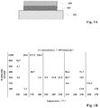
- Fig. 1A shows a schematic sectional view of a conductive wire bond pad comprising a Cr layer and an Au layer.
- the structure shown in Fig. 1A comprises a silicon nitride layer 101 (a film in the microphone), a Cr layer 102 on the silicon nitride layer 101, and an Au layer 103 on the Cr layer 102.
- Thermal processes for example, lithography, etching, and ashing processes all involve large amount of heat
- Cr may diffuse into the surface of the Au layer 103 and form chromium oxide (CrO x ) there, which may weaken the shear force of wire connections or even cause the bond to fail.
- first aspect of the present invention provides a semiconductor device manufacturing method.
- the method comprises: providing a substrate structure; forming a first metal layer on the substrate structure; forming a second metal layer on the first metal layer; forming a first oxide layer on the second metal layer at a first temperature; and conducting remaining manufacturing processes including thermal processes at a second temperature higher than the first temperature.
- the first oxide layer may comprise a silicon-based oxide, and the first temperature may be in a range of 170 °C to 210 °C.
- the thickness of the first oxide layer may be in a range of 1000 ⁇ to 20000 ⁇ .
- the first metal layer may comprise chromium and the second metal layer comprises gold.
- the first metal layer and the second metal layer may form a wire bond pad.
- the method may further comprise: removing the first oxide layer; and forming a metal wire on the second metal layer.
- the substrate structure may comprise: a substrate; a sacrificial material layer on the substrate; and a cover layer on the substrate covering the sacrificial material layer, wherein the first metal layer is formed on the cover layer.
- conducting remaining manufacturing processes including thermal processes may comprise: forming a patterned mask layer on a back side of the substrate; etching the substrate using the mask layer as a mask to form a through-hole that exposes the sacrificial material layer; and removing the mask layer.
- removing the first oxide layer may comprise: removing the sacrificial material layer through the through-hole by a Buffer Oxide Etching (BOE) method, wherein the first oxide layer is also removed by the BOE method.
- BOE Buffer Oxide Etching
- the method may further comprise: conducting a thickness reduction process on the back side of the substrate before the patterned mask layer is formed.
- concept second aspect of the present invention provides a semiconductor device.
- the device comprises: a substrate structure; a first metal layer on the substrate structure; a second metal layer on the first metal layer; and a first oxide layer on the second metal layer.
- the first oxide layer may comprise a silicon-based oxide formed in a temperature range of 170 °C to 210 °C.
- the thickness of the first oxide layer may be in a range of 1000 ⁇ to 20000 ⁇ .
- the first metal layer may comprise chromium
- the second metal layer may comprise gold
- the first metal layer and the second metal layer may form a wire bond pad.
- the substrate structure may comprise: a substrate; a sacrificial material layer on the substrate; and a cover layer on the substrate covering the sacrificial material layer, wherein the first metal layer is formed on the cover layer.
- a device according to the second aspect of the present invention may be obtained by a method according to the first aspect of the present invention.
- Embodiments in the figures may represent idealized illustrations. Variations from the shapes illustrated may be possible, for example due to manufacturing techniques and/or tolerances. Thus, the example embodiments shall not be construed as limited to the shapes or regions illustrated herein but are to include deviations in the shapes. For example, an etched region illustrated as a rectangle may have rounded or curved features. The shapes and regions illustrated in the figures are illustrative and shall not limit the invention.
- first,” “second,” etc. may be used herein to describe various elements, these elements shall not be limited by these terms. These terms may be used to distinguish one element from another element. Thus, a first element discussed below may be termed a second element without departing from the teachings of the present present invention. The description of an element as a “first” element may not require or imply the presence of a second element or other elements.
- the terms “first,” “second,” etc. may also be used herein to differentiate different categories or sets of elements. For conciseness, the terms “first,” “second,” etc. may represent “first-category (or first-set),” “second-category (or second-set),” etc., respectively.
- first element such as a layer, film, region, or substrate
- neighbored to or “coupled with” a second element
- the first element can be directly on, directly neighboring, directly connected to or directly coupled with the second element, or an intervening element may also be present between the first element and the second element.
- first element is referred to as being “directly on,” “directly neighboring,” “directly connected to,” or “directly coupled with” a second element, then no intended intervening element (except environmental elements such as air) may also be present between the first element and the second element.
- spatially relative terms such as “beneath,” “below,” “lower,” “above,” “upper,” and the like, may be used herein for ease of description to describe one element or feature's spatial relationship to another element(s) or feature(s) as illustrated in the figures. It will be understood that the spatially relative terms may encompass different orientations of the device in use or operation in addition to the orientation depicted in the figures. For example, if the device in the figures is turned over, elements described as “below” or “beneath” other elements or features would then be oriented “above” the other elements or features. Thus, the term “below” can encompass both an orientation of above and below. The device may be otherwise oriented (rotated 90 degrees or at other orientation), and the spatially relative descriptors used herein shall be interpreted accordingly.
- connection may mean “electrically connect.”
- insulation may mean “electrically insulate.”
- Embodiments of the present invention may also cover an article of manufacture that includes a non-transitory computer readable medium on which computer-readable instructions for carrying out embodiments of the inventive technique are stored.
- the computer readable medium may include, for example, semiconductor, magnetic, opto-magnetic, optical, or other forms of computer readable medium for storing computer readable code.
- the present invention may also cover apparatuses for practicing embodiments of the present invention. Such apparatus may include circuits, dedicated and/or programmable, to carry out operations pertaining to embodiments of the present invention.
- Examples of such apparatus include a general purpose computer and/or a dedicated computing device when appropriately programmed and may include a combination of a computer/computing device and dedicated/programmable hardware circuits (such as electrical, mechanical, and/or optical circuits) adapted for the various operations pertaining to embodiments of the present invention.
- a general purpose computer and/or a dedicated computing device when appropriately programmed and may include a combination of a computer/computing device and dedicated/programmable hardware circuits (such as electrical, mechanical, and/or optical circuits) adapted for the various operations pertaining to embodiments of the present invention.
- Fig. 1B is a table showing measured Cr concentrations on the surface of the Au layer in an exemplary wire bond pad comprising a Cr layer and an Au layer under different thermal conditions (e.g., different temperatures and/or different heating times).
- Fig. 1B shows that Cr concentration on the surface of the Au layer is 170 ⁇ 10 10 atoms/cm 2 when the temperature is 270 °C and the heating time is 180 seconds, and Cr concentration becomes 124.2 ⁇ 10 10 atoms/cm 2 when the temperature is 180 °C and the heating time is 1200 seconds.
- the Cr concentrations in these two examples are considered high, and the chromium oxide formed on the surface of the Au layer is detrimental to metal wire connections.
- Auger Electron Spectroscopy may also be used to measure Cr concentration on the surface of the Au layer for the embodiments of this present invention.
- SIMS Secondary Ion Mass Spectrometer
- TEM Transmission Electron Microscope
- Energy Dispersive X-Ray Spectroscopy may also be used to measure Cr concentration on the surface of the Au layer for the embodiments of this present invention.
- Fig. 2 shows a flowchart illustrating a semiconductor device manufacturing method in accordance with one or more embodiments of this present invention.
- a substrate structure is provided.
- the substrate structure may be a semiconductor structure on which a wire bond pad will be formed.
- the substrate structure may be a structure formed in a microphone manufacturing process.
- this present invention is not limited to a microphone manufacturing process and the substrate structure may be some other structures.
- a first metal layer is formed on the substrate structure.
- the first metal layer may comprise Cr and may have a thickness of several hundred angstrom.
- the first metal layer may have a thickness of 750 ⁇ .
- a second metal layer is formed on the first metal layer.
- the second metal layer may comprise Au and may have a thickness of several thousand angstrom.
- the second metal layer may have a thickness of 3000 ⁇ .
- the first metal layer and the second metal layer form a wire bond pad.
- a first oxide layer is formed on the second metal layer at a first temperature.
- the first oxide layer may comprise Low Temperature Oxide (LTO).
- the first oxide layer may comprise a silicon-based oxide such as tetraethoxysilane (TEOS) oxide or silane (SiH 4 ) oxide.
- the first temperature may be in a range of 170 °C to 210 °C.
- the first temperature may be 180°C, 190°C, or 200°C.
- the thickness of the first oxide layer may be in a range of 1000 ⁇ to 20000 ⁇ .
- the first oxide layer may have a thickness of 3000 ⁇ , 6000 ⁇ , 10000 A or 15000 ⁇ .
- step S210 the remaining manufacturing processes, including thermal processes, are conducted at a second temperature that is higher than the first temperature.
- the first oxide layer is formed on the second metal layer at the first temperature. Since the first temperature is lower than the second temperature at which the remaining manufacturing processes, including thermal processes, are conducted, the first oxide may fill in the grain boundary of the second metal layer, which lowers the concentration of the first metal that will diffuse to the surface of the second metal layer in the thermal processes, which in turn reduces the amount of the oxide of the first metal that will be formed on the surface of the second metal layer.
- the first oxide when a first oxide layer, such as an LTO layer, is formed on the surface of an Au layer, the first oxide may fill in the grain boundary of the Au layer and reduce the concentration of Cr that will diffuse to the surface of the Au layer, which in turn reduces the amount of chromium oxide that will be formed on the surface of the Au layer. This is beneficial to the establishment of metal wire connections after the first oxide layer is removed.
- a first oxide layer such as an LTO layer
- the manufacturing method may further comprise: removing the first oxide layer.
- the manufacturing method may further comprise: forming a metal wire on the second metal layer.
- the first oxide layer formed on the second metal layer in the preceding processes helps to reduce the amount of the oxide of the first metal that will be formed on the second metal layer, therefore it is beneficial to the establishment of metal wire connections on the second metal layer of the wire bond pad after the first oxide layer is removed.
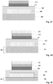
- FIGS. 3A, 3B , 3C, 3D , 3E , 3F, 3G, 3H , 3I, and 3J show schematic sectional views illustrating different stages of a semiconductor device manufacturing method in accordance with one or more embodiments of this present invention.
- Figs. 3A, 3B , 3C, 3D , 3E , 3F, 3G, 3H , 3I, and 3J show a process to form a wire bond pad in a microphone manufacturing process, thus this present invention will be herein described with references to this microphone manufacturing process.
- the substrate structure comprises a substrate 301 (such as a silicon substrate), a sacrificial material layer 302 (such as a silicon oxide layer) on the substrate 301, and a cover layer 303 (such as a silicon nitride layer) on the substrate 301 covering the sacrificial material layer 302.
- a substrate 301 such as a silicon substrate
- a sacrificial material layer 302 such as a silicon oxide layer
- a cover layer 303 such as a silicon nitride layer
- Fig. 3A does not show some films or structures, such as the electrode plate and the vibration film, of a microphone. These omissions, however, do not prevent one of ordinary skill in the art in this field to make and use the present invention herein disclosed.
- a first metal layer 311 is formed on the substrate structure.
- the first metal layer 311 may comprise Cr and may be formed on the cover layer 303 by deposition.
- a second metal layer 312 is formed on the first metal layer 311.
- the second metal layer 312 may comprise Au and may be formed on the first metal layer 311 by deposition.
- a first oxide layer 321 is formed on the second metal layer 312 by deposition at a first temperature.
- the first oxide layer 321 comprises Low Temperature Oxide (LTO).
- the first oxide layer 321 may comprise a silicon-based oxide, and the first temperature may be in a range of 170 °C to 210°C.
- the first temperature may be 180 °C, 190 °C, or 200 °C.
- the thickness of the first oxide layer 321 may be in a range of 1000 ⁇ to 20000 ⁇ .
- the first oxide layer 321 may have a thickness of 3000 ⁇ , 6000 ⁇ , 10000 ⁇ or 15000 ⁇ .
- a thickness reduction process may be applied on a backside of the substrate 301, which is a side of the substrate 301 that is opposite the side on which the first metal layer 311 is formed.
- the thickness reduction process may reduce the thickness of the substrate 301 from H0 as shown in Fig. 3D , to H1 as shown in Fig. 3E , wherein H1 is smaller than H0.
- the thickness reduction process may reduce the thickness of the substrate 301 from 725 ⁇ to 400 ⁇ .
- Figs. 3F, 3G, and 3H illustrate conducting the remaining manufacturing processes including thermal processes in accordance with one or more embodiments of this present invention.
- the remaining manufacturing processes including thermal processes may comprise forming a patterned mask layer 325 (such as a photoresist layer) on the back side of the substrate 301, as shown in Fig. 3F ; and etching the substrate 301 using the mask layer 325 as a mask to form a through-hole 330 that exposes the sacrificial material layer 302, as shown in Fig. 3G .
- a plurality of the through-holes 330 may be formed, as shown in Fig. 3G .
- the remaining manufacturing processes may further comprise removing the mask layer 325 through an ashing process, as shown in Fig. 3H .
- the processes to form the mask layer 325, to etch the substrate 301, and to remove the mask layer 325 may all be conducted in a high temperature environment, which may cause the first metal (e.g. Cr) to diffuse into the surface of the second metal layer (e.g. Au).
- the first metal e.g. Cr
- the second metal layer e.g. Au
- the first oxide layer 321 e.g. the LTO layer
- the first oxide may fill in the grain boundary of the second metal layer and lower the concentration of the first metal that will diffuse to the surface of the second metal layer, which in turn reduces the amount of the oxide of the first metal that will be formed on the surface of the second metal layer.
- a cavity is formed by removing the sacrificial material layer 302 through the through-holes 330 by a BOE method.
- the first oxide layer 321 may also be removed by the BOE method in this step.
- the first oxide layer is an LTO layer that comprises low temperature deposition oxide that has a loose structure, so it can be easily removed by the BOE method.
- a metal wire 340 is formed on the second metal layer 312.
- the metal wire 340 may be made of a metallic material such as aluminum, copper, or tungsten, and can be used as a connection wire.
- This manufacturing method forms a wire bond pad that can be used for metal wire connections in a microphone.
- This manufacturing method can lower the concentration of the first metal diffused into the surface of the second metal in the thermal processes. For example, it reduces the concentration of Cr diffused into the surface of the Au layer, thus reducing the amount of the oxide of the first metal (e.g. chromium oxide) formed during the process. Therefore, the method is beneficial to the establishment of metal wire connections.
- the first metal e.g. chromium oxide
- Fig. 4 shows a graph illustrating measured Cr concentrations on the surface of the Au layer on different examples.
- Fig. 4 shows data obtained under two different conditions, one with an LTO layer formed on the surface of the Au layer (labeled with "LTO+”) and the other without.
- Cr concentration on the surface of the Au layer is 170 . 4 ⁇ 10 10 atoms/cm 2 when there is no LTO layer formed on the Au layer, and Cr concentration reduces to 52.6 ⁇ 10 10 atoms/cm 2 when there is an LTO layer.
- Cr concentration on the surface of the Au layer is 124.4 ⁇ 10 10 atoms/cm 2 when there is no LTO layer formed on the Au layer, and Cr concentration reduces to 58.5 ⁇ 10 10 atoms/cm 2 when there is an LTO layer. Therefore the existence of an LTO layer on the surface of the Au layer dramatically reduces Cr concentration on the surface of the Au layer.
- this present invention further presents a semiconductor device.
- this semiconductor device comprises a substrate structure comprising a substrate 301, a sacrificial material layer 302 on the substrate 301, and a cover layer 303 on the substrate 201 covering the sacrificial material layer 302.
- this semiconductor device further comprises a first metal layer 311 on the substrate structure.
- the first metal layer 311 may comprise Cr and may be formed on the cover layer 303.
- this semiconductor device further comprises a second metal layer 312 on the first metal layer 311.
- the second metal layer 312 may comprise Au.
- the first metal layer 311 and the second metal layer 312 form a wire bond pad for metal wire connections.
- this semiconductor device further comprises a first oxide layer 321 on the second metal layer 312.
- the first oxide layer 321 may be an LTO layer.
- the first oxide layer 321 may comprise a silicon-based oxide formed in a temperature range of 170 °C to 210 °C (e.g. 180 °C, 190 °C, or 200 °C).
- the thickness of the first oxide layer 321 is in a range of 1000 ⁇ to 20000 ⁇ .
- the first oxide layer 321 may have a thickness of 3000 ⁇ , 6000 ⁇ , 10000 ⁇ or 15000 ⁇ .
- the semiconductor device of this present invention can reduce the concentration of the first metal diffused into the surface of the second metal layer in the manufacturing processes including thermal processes. For example, it can reduce the concentration of Cr diffused into the surface of the Au layer, therefore it is beneficial to the establishment of metal wire connections on the second metal layer after the first oxide layer is removed.
Landscapes
- Engineering & Computer Science (AREA)
- Physics & Mathematics (AREA)
- Acoustics & Sound (AREA)
- Signal Processing (AREA)
- Microelectronics & Electronic Packaging (AREA)
- Manufacturing & Machinery (AREA)
- Computer Hardware Design (AREA)
- Internal Circuitry In Semiconductor Integrated Circuit Devices (AREA)
- Chemical & Material Sciences (AREA)
- Inorganic Chemistry (AREA)
Abstract
Description
- This application claims priority to and benefit of Chinese Patent Application No.
201611066885.0 filed on November 29, 2016 - This present invention relates to semiconductor technology and, more specifically, to semiconductor device and its manufacturing method.
- In a microphone manufacturing process, a wire bond pad connecting different wires typically comprises chromium (Cr) and gold (Au).
Fig. 1A shows a schematic sectional view of a conductive wire bond pad comprising a Cr layer and an Au layer. The structure shown inFig. 1A comprises a silicon nitride layer 101 (a film in the microphone), aCr layer 102 on thesilicon nitride layer 101, and anAu layer 103 on theCr layer 102. Thermal processes (for example, lithography, etching, and ashing processes all involve large amount of heat) that need to be conducted after the wire bond pad is built may cause Cr to diffuse into the surface of theAu layer 103 and form chromium oxide (CrOx) there, which may weaken the shear force of wire connections or even cause the bond to fail. - Conventional methods lower the diffusion activity of Cr, and thus prevent Cr from diffusing into the surface of the Au layer, by capping the peak temperature in the succeeding processes. However, without a sufficiently high temperature in the succeeding processes, the polymer in Deep Reactive Ion Etching (DRIE) cannot be completely removed, and the polymer residue may cause detection problems in the Buffer Oxide Etching (BOE) process.
- It is an object of the present invention to propose a solution remedying at least one of the drawbacks of the conventional methods.
- The object is achieved by the features of the respective independent claims. Further embodiments and developments are defined in the dependent claims.
- concept first aspect of the present invention provides a semiconductor device manufacturing method. The method comprises: providing a substrate structure; forming a first metal layer on the substrate structure; forming a second metal layer on the first metal layer; forming a first oxide layer on the second metal layer at a first temperature; and conducting remaining manufacturing processes including thermal processes at a second temperature higher than the first temperature.
- Preferably, the first oxide layer may comprise a silicon-based oxide, and the first temperature may be in a range of 170 °C to 210 °C.
- Preferably, the thickness of the first oxide layer may be in a range of 1000 Å to 20000 Å.
- Preferably, the first metal layer may comprise chromium and the second metal layer comprises gold.
- Preferably, the first metal layer and the second metal layer may form a wire bond pad.
- Preferably, the method may further comprise: removing the first oxide layer; and forming a metal wire on the second metal layer.
- Preferably, the substrate structure may comprise: a substrate; a sacrificial material layer on the substrate; and a cover layer on the substrate covering the sacrificial material layer, wherein the first metal layer is formed on the cover layer.
- Preferably, conducting remaining manufacturing processes including thermal processes may comprise: forming a patterned mask layer on a back side of the substrate; etching the substrate using the mask layer as a mask to form a through-hole that exposes the sacrificial material layer; and removing the mask layer.
- Preferably, removing the first oxide layer may comprise: removing the sacrificial material layer through the through-hole by a Buffer Oxide Etching (BOE) method, wherein the first oxide layer is also removed by the BOE method.
- Preferably, the method may further comprise: conducting a thickness reduction process on the back side of the substrate before the patterned mask layer is formed.
concept second aspect of the present invention provides a semiconductor device. The device comprises: a substrate structure; a first metal layer on the substrate structure; a second metal layer on the first metal layer; and a first oxide layer on the second metal layer. - Preferably, the first oxide layer may comprise a silicon-based oxide formed in a temperature range of 170 °C to 210 °C.
- Preferably, the thickness of the first oxide layer may be in a range of 1000 Å to 20000 Å.
- Preferably, the first metal layer may comprise chromium, and the second metal layer may comprise gold.
- Preferably, the first metal layer and the second metal layer may form a wire bond pad.
- Preferably, the substrate structure may comprise: a substrate; a sacrificial material layer on the substrate; and a cover layer on the substrate covering the sacrificial material layer, wherein the first metal layer is formed on the cover layer.
- A device according to the second aspect of the present invention may be obtained by a method according to the first aspect of the present invention.
- The drawings illustrate some embodiments of this present invention and will be used to describe this present invention along with the specification.
-
Fig. 1A shows a schematic sectional view of a conductive wire bond pad comprising a chromium (Cr) layer and a gold (Au) layer. -
Fig. 1B is a table showing measured Cr concentrations on the surface of the Au layer in an exemplary wire bond pad comprising a Cr layer and an Au layer. -
Fig. 2 shows a flowchart illustrating a semiconductor device manufacturing method in accordance with one or more embodiments of this present invention. -
Figs. 3A, 3B ,3C, 3D ,3E ,3F, 3G, 3H ,3I, and 3J show schematic sectional views illustrating different stages of a semiconductor device manufacturing method in accordance with one or more embodiments of this present invention. -
Fig. 4 shows a graph illustrating measured Cr concentrations on the surface of the Au layer on different examples. - Example embodiments of the present invention are described with reference to the accompanying drawings. As those skilled in the art would realize, the described embodiments may be modified in various ways without departing from the present invention. Embodiments may be practiced without some or all of these specified details. Well known process steps and/or structures may not be described in detail, in the interest of clarity.
- The drawings and descriptions are illustrative and not restrictive. Like reference numerals may designate like (e.g., analogous or identical) elements in the specification. To the extent possible, any repetitive description will be minimized.
- Relative sizes and thicknesses of elements shown in the drawings are chosen to facilitate description and understanding, without limiting the present invention. In the drawings, the thicknesses of some layers, films, panels, regions, etc., may be exaggerated for clarity.
- Embodiments in the figures may represent idealized illustrations. Variations from the shapes illustrated may be possible, for example due to manufacturing techniques and/or tolerances. Thus, the example embodiments shall not be construed as limited to the shapes or regions illustrated herein but are to include deviations in the shapes. For example, an etched region illustrated as a rectangle may have rounded or curved features. The shapes and regions illustrated in the figures are illustrative and shall not limit the invention.
- Although the terms "first," "second," etc. may be used herein to describe various elements, these elements shall not be limited by these terms. These terms may be used to distinguish one element from another element. Thus, a first element discussed below may be termed a second element without departing from the teachings of the present present invention. The description of an element as a "first" element may not require or imply the presence of a second element or other elements. The terms "first," "second," etc. may also be used herein to differentiate different categories or sets of elements. For conciseness, the terms "first," "second," etc. may represent "first-category (or first-set)," "second-category (or second-set)," etc., respectively.
- If a first element (such as a layer, film, region, or substrate) is referred to as being "on," "neighboring," "connected to," or "coupled with" a second element, then the first element can be directly on, directly neighboring, directly connected to or directly coupled with the second element, or an intervening element may also be present between the first element and the second element. If a first element is referred to as being "directly on," "directly neighboring," "directly connected to," or "directly coupled with" a second element, then no intended intervening element (except environmental elements such as air) may also be present between the first element and the second element.
- Spatially relative terms, such as "beneath," "below," "lower," "above," "upper," and the like, may be used herein for ease of description to describe one element or feature's spatial relationship to another element(s) or feature(s) as illustrated in the figures. It will be understood that the spatially relative terms may encompass different orientations of the device in use or operation in addition to the orientation depicted in the figures. For example, if the device in the figures is turned over, elements described as "below" or "beneath" other elements or features would then be oriented "above" the other elements or features. Thus, the term "below" can encompass both an orientation of above and below. The device may be otherwise oriented (rotated 90 degrees or at other orientation), and the spatially relative descriptors used herein shall be interpreted accordingly.
- The terminology used herein is for the purpose of describing particular embodiments and is not intended to limit the present invention. As used herein, singular forms, "a," "an," and "the" may indicate plural forms as well, unless the context clearly indicates otherwise. The terms "includes" and/or "including," when used in this specification, may specify the presence of stated features, integers, steps, operations, elements, and/or components, but may not preclude the presence or addition of one or more other features, integers, steps, operations, elements, components, and/or groups.
- Unless otherwise defined, terms (including technical and scientific terms) used herein have the same meanings as what is commonly understood by one of ordinary skill in the art related to this field. Terms, such as those defined in commonly used dictionaries, shall be interpreted as having meanings that are consistent with their meanings in the context of the relevant art and shall not be interpreted in an idealized or overly formal sense unless expressly so defined herein.
- The term "connect" may mean "electrically connect." The term "insulate" may mean "electrically insulate."
- Unless explicitly described as being otherwise, the word "comprise" and variations such as "comprises," "comprising," "include," or "including" may imply the inclusion of stated elements but not the exclusion of other elements.
- Various embodiments, including methods and techniques, are described in this disclosure. Embodiments of the present invention may also cover an article of manufacture that includes a non-transitory computer readable medium on which computer-readable instructions for carrying out embodiments of the inventive technique are stored. The computer readable medium may include, for example, semiconductor, magnetic, opto-magnetic, optical, or other forms of computer readable medium for storing computer readable code. Further, the present invention may also cover apparatuses for practicing embodiments of the present invention. Such apparatus may include circuits, dedicated and/or programmable, to carry out operations pertaining to embodiments of the present invention. Examples of such apparatus include a general purpose computer and/or a dedicated computing device when appropriately programmed and may include a combination of a computer/computing device and dedicated/programmable hardware circuits (such as electrical, mechanical, and/or optical circuits) adapted for the various operations pertaining to embodiments of the present invention.
- The inventors of this present invention use Total Reflection X-Ray Fluorescence (TXRF) to measure Cr concentration on the surface of the Au layer.
Fig. 1B is a table showing measured Cr concentrations on the surface of the Au layer in an exemplary wire bond pad comprising a Cr layer and an Au layer under different thermal conditions (e.g., different temperatures and/or different heating times). For example,Fig. 1B shows that Cr concentration on the surface of the Au layer is 170× 1010atoms/cm2 when the temperature is 270 °C and the heating time is 180 seconds, and Cr concentration becomes 124.2× 10¹⁰ atoms/cm2 when the temperature is 180 °C and the heating time is 1200 seconds. The Cr concentrations in these two examples are considered high, and the chromium oxide formed on the surface of the Au layer is detrimental to metal wire connections. - In some other embodiments, other methods, such as Auger Electron Spectroscopy, Secondary Ion Mass Spectrometer (SIMS), Transmission Electron Microscope (TEM), and Energy Dispersive X-Ray Spectroscopy, may also be used to measure Cr concentration on the surface of the Au layer for the embodiments of this present invention.
-
Fig. 2 shows a flowchart illustrating a semiconductor device manufacturing method in accordance with one or more embodiments of this present invention. - In step S202, a substrate structure is provided. The substrate structure may be a semiconductor structure on which a wire bond pad will be formed. For example, the substrate structure may be a structure formed in a microphone manufacturing process. However, it should be understood that this present invention is not limited to a microphone manufacturing process and the substrate structure may be some other structures.
- In step S204, a first metal layer is formed on the substrate structure. The first metal layer may comprise Cr and may have a thickness of several hundred angstrom. For example, the first metal layer may have a thickness of 750 Å.
- In step S206, a second metal layer is formed on the first metal layer. The second metal layer may comprise Au and may have a thickness of several thousand angstrom. For example, the second metal layer may have a thickness of 3000 Å. The first metal layer and the second metal layer form a wire bond pad.
- In step S208, a first oxide layer is formed on the second metal layer at a first temperature. In one embodiment, the first oxide layer may comprise Low Temperature Oxide (LTO). For example, the first oxide layer may comprise a silicon-based oxide such as tetraethoxysilane (TEOS) oxide or silane (SiH4) oxide. The first temperature may be in a range of 170 °C to 210 °C. For example, the first temperature may be 180°C, 190°C, or 200°C. In one embodiment, the thickness of the first oxide layer may be in a range of 1000 Å to 20000 Å. For example, the first oxide layer may have a thickness of 3000 Å, 6000 Å, 10000 A or 15000 Å.
- In step S210, the remaining manufacturing processes, including thermal processes, are conducted at a second temperature that is higher than the first temperature.
- In one embodiment, the first oxide layer is formed on the second metal layer at the first temperature. Since the first temperature is lower than the second temperature at which the remaining manufacturing processes, including thermal processes, are conducted, the first oxide may fill in the grain boundary of the second metal layer, which lowers the concentration of the first metal that will diffuse to the surface of the second metal layer in the thermal processes, which in turn reduces the amount of the oxide of the first metal that will be formed on the surface of the second metal layer.
- For example, when a first oxide layer, such as an LTO layer, is formed on the surface of an Au layer, the first oxide may fill in the grain boundary of the Au layer and reduce the concentration of Cr that will diffuse to the surface of the Au layer, which in turn reduces the amount of chromium oxide that will be formed on the surface of the Au layer. This is beneficial to the establishment of metal wire connections after the first oxide layer is removed.
- In some embodiments, the manufacturing method may further comprise: removing the first oxide layer. Optionally, after the first oxide layer is removed, the manufacturing method may further comprise: forming a metal wire on the second metal layer. The first oxide layer formed on the second metal layer in the preceding processes helps to reduce the amount of the oxide of the first metal that will be formed on the second metal layer, therefore it is beneficial to the establishment of metal wire connections on the second metal layer of the wire bond pad after the first oxide layer is removed.
-
Figs. 3A, 3B ,3C, 3D ,3E ,3F, 3G, 3H ,3I, and 3J show schematic sectional views illustrating different stages of a semiconductor device manufacturing method in accordance with one or more embodiments of this present invention.Figs. 3A, 3B ,3C, 3D ,3E ,3F, 3G, 3H ,3I, and 3J show a process to form a wire bond pad in a microphone manufacturing process, thus this present invention will be herein described with references to this microphone manufacturing process. - Referring to
Fig. 3A , a substrate structure is provided. The substrate structure comprises a substrate 301 (such as a silicon substrate), a sacrificial material layer 302 (such as a silicon oxide layer) on thesubstrate 301, and a cover layer 303 (such as a silicon nitride layer) on thesubstrate 301 covering thesacrificial material layer 302. - It should be understood that, for the purpose of conciseness and convenience, some components or details that are well known to one of ordinary skill in the art in this field are omitted in the drawings of this application. For example,
Fig. 3A does not show some films or structures, such as the electrode plate and the vibration film, of a microphone. These omissions, however, do not prevent one of ordinary skill in the art in this field to make and use the present invention herein disclosed. - Referring to
Fig. 3B , afirst metal layer 311 is formed on the substrate structure. Thefirst metal layer 311 may comprise Cr and may be formed on thecover layer 303 by deposition. - Referring to
Fig. 3C , asecond metal layer 312 is formed on thefirst metal layer 311. Thesecond metal layer 312 may comprise Au and may be formed on thefirst metal layer 311 by deposition. - Referring to
Fig. 3D , afirst oxide layer 321 is formed on thesecond metal layer 312 by deposition at a first temperature. In one embodiment, thefirst oxide layer 321 comprises Low Temperature Oxide (LTO). Thefirst oxide layer 321 may comprise a silicon-based oxide, and the first temperature may be in a range of 170 °C to 210°C. For example, the first temperature may be 180 °C, 190 °C, or 200 °C. In one embodiment, the thickness of thefirst oxide layer 321 may be in a range of 1000 Å to 20000 Å. For example, thefirst oxide layer 321 may have a thickness of 3000 Å, 6000 Å, 10000 Å or 15000 Å. - Referring to
Fig. 3E , optionally, a thickness reduction process may be applied on a backside of thesubstrate 301, which is a side of thesubstrate 301 that is opposite the side on which thefirst metal layer 311 is formed. For example, the thickness reduction process may reduce the thickness of thesubstrate 301 from H0 as shown inFig. 3D , to H1 as shown inFig. 3E , wherein H1 is smaller than H0. For example, the thickness reduction process may reduce the thickness of thesubstrate 301 from 725 Å to 400 Å. - Next, the remaining manufacturing processes including thermal process are conducted.
Figs. 3F, 3G, and 3H illustrate conducting the remaining manufacturing processes including thermal processes in accordance with one or more embodiments of this present invention. - The remaining manufacturing processes including thermal processes may comprise forming a patterned mask layer 325 (such as a photoresist layer) on the back side of the
substrate 301, as shown inFig. 3F ; and etching thesubstrate 301 using themask layer 325 as a mask to form a through-hole 330 that exposes thesacrificial material layer 302, as shown inFig. 3G . A plurality of the through-holes 330 may be formed, as shown inFig. 3G . The remaining manufacturing processes may further comprise removing themask layer 325 through an ashing process, as shown inFig. 3H . - In the manufacturing processes just described, the processes to form the
mask layer 325, to etch thesubstrate 301, and to remove themask layer 325 may all be conducted in a high temperature environment, which may cause the first metal (e.g. Cr) to diffuse into the surface of the second metal layer (e.g. Au). However, since a first oxide layer 321 (e.g. the LTO layer) has been formed on thesecond metal layer 312, the first oxide may fill in the grain boundary of the second metal layer and lower the concentration of the first metal that will diffuse to the surface of the second metal layer, which in turn reduces the amount of the oxide of the first metal that will be formed on the surface of the second metal layer. - Referring to
Fig. 3I , a cavity is formed by removing thesacrificial material layer 302 through the through-holes 330 by a BOE method. Thefirst oxide layer 321 may also be removed by the BOE method in this step. In some embodiments, the first oxide layer is an LTO layer that comprises low temperature deposition oxide that has a loose structure, so it can be easily removed by the BOE method. - Referring to
Fig. 3J , ametal wire 340 is formed on thesecond metal layer 312. Themetal wire 340 may be made of a metallic material such as aluminum, copper, or tungsten, and can be used as a connection wire. - This concludes a semiconductor device manufacturing method in accordance with one or more embodiments of this present invention. This manufacturing method forms a wire bond pad that can be used for metal wire connections in a microphone. This manufacturing method can lower the concentration of the first metal diffused into the surface of the second metal in the thermal processes. For example, it reduces the concentration of Cr diffused into the surface of the Au layer, thus reducing the amount of the oxide of the first metal (e.g. chromium oxide) formed during the process. Therefore, the method is beneficial to the establishment of metal wire connections.
-
Fig. 4 shows a graph illustrating measured Cr concentrations on the surface of the Au layer on different examples.Fig. 4 shows data obtained under two different conditions, one with an LTO layer formed on the surface of the Au layer (labeled with "LTO+") and the other without. - As shown in
Fig. 4 , at a temperature of 270 °C and a heating time of 180 seconds, Cr concentration on the surface of the Au layer is 170.4× 10¹⁰ atoms/cm2 when there is no LTO layer formed on the Au layer, and Cr concentration reduces to 52.6× 10¹⁰ atoms/cm2 when there is an LTO layer. In another example, at a temperature of 180 °C and a heating time of 1200 seconds, Cr concentration on the surface of the Au layer is 124.4× 10¹⁰ atoms/cm2 when there is no LTO layer formed on the Au layer, and Cr concentration reduces to 58.5× 10¹⁰ atoms/cm2 when there is an LTO layer. Therefore the existence of an LTO layer on the surface of the Au layer dramatically reduces Cr concentration on the surface of the Au layer. - This present invention further presents a semiconductor device. Referring to
Fig. 3D , this semiconductor device comprises a substrate structure comprising asubstrate 301, asacrificial material layer 302 on thesubstrate 301, and acover layer 303 on the substrate 201 covering thesacrificial material layer 302. - Referring to
Fig. 3D , this semiconductor device further comprises afirst metal layer 311 on the substrate structure. Thefirst metal layer 311 may comprise Cr and may be formed on thecover layer 303. - Referring to
Fig. 3D , this semiconductor device further comprises asecond metal layer 312 on thefirst metal layer 311. Thesecond metal layer 312 may comprise Au. In one embodiment, thefirst metal layer 311 and thesecond metal layer 312 form a wire bond pad for metal wire connections. - Referring to
Fig. 3D , this semiconductor device further comprises afirst oxide layer 321 on thesecond metal layer 312. Thefirst oxide layer 321 may be an LTO layer. For example, thefirst oxide layer 321 may comprise a silicon-based oxide formed in a temperature range of 170 °C to 210 °C (e.g. 180 °C, 190 °C, or 200 °C). In one embodiment, the thickness of thefirst oxide layer 321 is in a range of 1000 Å to 20000 Å. For example, thefirst oxide layer 321 may have a thickness of 3000 Å, 6000 Å, 10000 Å or 15000 Å. - The semiconductor device of this present invention can reduce the concentration of the first metal diffused into the surface of the second metal layer in the manufacturing processes including thermal processes. For example, it can reduce the concentration of Cr diffused into the surface of the Au layer, therefore it is beneficial to the establishment of metal wire connections on the second metal layer after the first oxide layer is removed.
- This concludes the description of a semiconductor device and its manufacturing method in accordance with one or more embodiments of this present invention. For the purpose of conciseness and convenience, some components or procedures that are well known to one of ordinary skill in the art in this field are omitted. These omissions, however, do not prevent one of ordinary skill in the art in this field to make and use the present invention herein disclosed.
Claims (15)
- A semiconductor device manufacturing method, comprising:providing a substrate structure;forming a first metal layer on the substrate structure;forming a second metal layer on the first metal layer;forming a first oxide layer on the second metal layer at a first temperature; andconducting remaining manufacturing processes including thermal processes at a second temperature higher than the first temperature.
- The method of claim 1, wherein
the first oxide layer comprises a silicon-based oxide, and the first temperature is in a range of 170 °C to 210 °C; and/or
the thickness of the first oxide layer is in a range of 1000 Å to 20000 Å. - The method of claim 1 or 2, wherein the first metal layer comprises chromium and the second metal layer comprises gold.
- The method of any one of the claims 1-3, wherein the first metal layer and the second metal layer form a wire bond pad.
- The method of any one of the claims 1-4, further comprising:removing the first oxide layer; andforming a metal wire on the second metal layer.
- The method of claim 5, wherein the substrate structure comprises:a substrate;a sacrificial material layer on the substrate; anda cover layer on the substrate covering the sacrificial material layer, wherein the first metal layer is formed on the cover layer.
- The method of claim 6, wherein conducting remaining manufacturing processes including thermal processes comprises:forming a patterned mask layer on a back side of the substrate;etching the substrate using the mask layer as a mask to form a through-hole that exposes the sacrificial material layer; andremoving the mask layer.
- The method of claim 7, wherein removing the first oxide layer comprises:removing the sacrificial material layer through the through-hole by a Buffer Oxide Etching, BOE, method, wherein the first oxide layer is also removed by the BOE method.
- The method of claim 7 or 8, further comprises:conducting a thickness reduction process on the back side of the substrate before the patterned mask layer is formed.
- A semiconductor device, comprising:a substrate structure;a first metal layer on the substrate structure;a second metal layer on the first metal layer; anda first oxide layer on the second metal layer.
- The semiconductor device of claim 10, wherein the first oxide layer comprises a silicon-based oxide formed in a temperature range of 170 °C to 210 °C.
- The semiconductor device of claim 10 or 11, wherein the thickness of the first oxide layer is in a range of 1000 Å to 20000 Å.
- The semiconductor device of any one of the claims 10-12, wherein the first metal layer comprises chromium, and the second metal layer comprises gold.
- The semiconductor device of any one of the claims 10-13, wherein the first metal layer and the second metal layer form a wire bond pad.
- The semiconductor device of any one of the claims 10-14, wherein the substrate structure comprises:a substrate;a sacrificial material layer on the substrate; anda cover layer on the substrate covering the sacrificial material layer, wherein the first metal layer is formed on the cover layer.
Applications Claiming Priority (1)
| Application Number | Priority Date | Filing Date | Title |
|---|---|---|---|
| CN201611066885.0A CN108122790B (en) | 2016-11-29 | 2016-11-29 | Semiconductor device and method of manufacturing the same |
Publications (2)
| Publication Number | Publication Date |
|---|---|
| EP3328094A1 true EP3328094A1 (en) | 2018-05-30 |
| EP3328094B1 EP3328094B1 (en) | 2020-05-06 |
Family
ID=60480211
Family Applications (1)
| Application Number | Title | Priority Date | Filing Date |
|---|---|---|---|
| EP17203760.8A Active EP3328094B1 (en) | 2016-11-29 | 2017-11-27 | A semiconductor device and manufacture thereof |
Country Status (3)
| Country | Link |
|---|---|
| US (2) | US10587971B2 (en) |
| EP (1) | EP3328094B1 (en) |
| CN (1) | CN108122790B (en) |
Families Citing this family (1)
| Publication number | Priority date | Publication date | Assignee | Title |
|---|---|---|---|---|
| CN111908420B (en) * | 2019-05-09 | 2024-02-27 | 无锡华润上华科技有限公司 | Microelectromechanical system device preparation method |
Citations (4)
| Publication number | Priority date | Publication date | Assignee | Title |
|---|---|---|---|---|
| US5708302A (en) * | 1995-04-26 | 1998-01-13 | Symetrix Corporation | Bottom electrode structure for dielectric capacitors |
| US20040147132A1 (en) * | 2002-09-26 | 2004-07-29 | Yun-Woo Nam | Flexible MEMS transducer manufacturing method |
| US20070096300A1 (en) * | 2005-10-28 | 2007-05-03 | Hsin-Fu Wang | Diffusion barrier layer for MEMS devices |
| US20160268084A1 (en) * | 2015-03-11 | 2016-09-15 | Innovative Micro Technology | Dual substrate electrostatic mems switch with multiple hinges and method of manufacture |
Family Cites Families (19)
| Publication number | Priority date | Publication date | Assignee | Title |
|---|---|---|---|---|
| US6350643B1 (en) * | 1997-12-18 | 2002-02-26 | Advanced Technology Materials, Inc. | Reduced degradation of metal oxide ceramic due to diffusion of a mobile specie therefrom |
| KR100578976B1 (en) * | 2004-10-15 | 2006-05-12 | 삼성에스디아이 주식회사 | Multilayer Thin Film with Excellent Adhesion and Manufacturing Method Thereof |
| JP4742972B2 (en) * | 2006-04-27 | 2011-08-10 | オムロン株式会社 | Microphone manufacturing method |
| JP4144640B2 (en) * | 2006-10-13 | 2008-09-03 | オムロン株式会社 | Method for manufacturing vibration sensor |
| KR101910978B1 (en) * | 2011-06-22 | 2018-10-24 | 삼성전자주식회사 | Nano-sensor and method of manufacturing the same |
| US8633634B2 (en) * | 2011-11-18 | 2014-01-21 | The Board Of Regents Of The University Of Texas System | MEMs-based cantilever energy harvester |
| KR101902267B1 (en) * | 2012-02-17 | 2018-09-28 | 삼성전자주식회사 | Nano scale resonator and nano scale sensor and fabrication method thereof |
| US9758821B2 (en) * | 2012-04-17 | 2017-09-12 | International Business Machines Corporation | Graphene transistor gated by charges through a nanopore for bio-molecular sensing and DNA sequencing |
| US9548332B2 (en) * | 2012-04-27 | 2017-01-17 | Apple Inc. | Method of forming a micro LED device with self-aligned metallization stack |
| WO2014085787A1 (en) * | 2012-11-30 | 2014-06-05 | The Regents Of The University Of California | Silicon microsystems for high-throughput analysis of neural circuit activity, method and process for making the same |
| US8946779B2 (en) * | 2013-02-26 | 2015-02-03 | Freescale Semiconductor, Inc. | MISHFET and Schottky device integration |
| CN103367116B (en) * | 2013-06-28 | 2017-07-11 | 上海华虹宏力半导体制造有限公司 | High-density capacitor structure and preparation method thereof |
| JP6136701B2 (en) * | 2013-07-24 | 2017-05-31 | 日亜化学工業株式会社 | Light emitting device |
| US9450147B2 (en) * | 2013-12-27 | 2016-09-20 | Apple Inc. | LED with internally confined current injection area |
| US9318718B2 (en) * | 2014-05-13 | 2016-04-19 | King Abdullah University Of Science And Technology | Methods and devices for silicon integrated vertically aligned field effect transistors |
| JP6661283B2 (en) * | 2015-05-14 | 2020-03-11 | 東京エレクトロン株式会社 | Cleaning method and plasma processing method |
| US10181428B2 (en) * | 2015-08-28 | 2019-01-15 | Skyworks Solutions, Inc. | Silicon on porous silicon |
| US9704839B2 (en) * | 2015-11-18 | 2017-07-11 | Infineon Technologies Ag | Semiconductor devices for integration with light emitting chips and modules thereof |
| US9847221B1 (en) * | 2016-09-29 | 2017-12-19 | Lam Research Corporation | Low temperature formation of high quality silicon oxide films in semiconductor device manufacturing |
-
2016
- 2016-11-29 CN CN201611066885.0A patent/CN108122790B/en active Active
-
2017
- 2017-11-27 EP EP17203760.8A patent/EP3328094B1/en active Active
- 2017-11-28 US US15/824,716 patent/US10587971B2/en active Active
-
2019
- 2019-12-30 US US16/730,569 patent/US11109171B2/en active Active
Patent Citations (4)
| Publication number | Priority date | Publication date | Assignee | Title |
|---|---|---|---|---|
| US5708302A (en) * | 1995-04-26 | 1998-01-13 | Symetrix Corporation | Bottom electrode structure for dielectric capacitors |
| US20040147132A1 (en) * | 2002-09-26 | 2004-07-29 | Yun-Woo Nam | Flexible MEMS transducer manufacturing method |
| US20070096300A1 (en) * | 2005-10-28 | 2007-05-03 | Hsin-Fu Wang | Diffusion barrier layer for MEMS devices |
| US20160268084A1 (en) * | 2015-03-11 | 2016-09-15 | Innovative Micro Technology | Dual substrate electrostatic mems switch with multiple hinges and method of manufacture |
Also Published As
| Publication number | Publication date |
|---|---|
| US20180152801A1 (en) | 2018-05-31 |
| US20200145771A1 (en) | 2020-05-07 |
| US10587971B2 (en) | 2020-03-10 |
| CN108122790B (en) | 2020-12-18 |
| EP3328094B1 (en) | 2020-05-06 |
| US11109171B2 (en) | 2021-08-31 |
| CN108122790A (en) | 2018-06-05 |
Similar Documents
| Publication | Publication Date | Title |
|---|---|---|
| US8604618B2 (en) | Structure and method for reducing vertical crack propagation | |
| DE102009012594B4 (en) | Through-substrate-via-semiconductor components | |
| US20220328353A1 (en) | Through electrode substrate, method of manufacturing through electrode substrate, and mounting substrate | |
| EP3232570A2 (en) | Thin-film bulk acoustic resonator, semiconductor apparatus comprising of such an acoustic resonator, and manufacture thereof | |
| US9159699B2 (en) | Interconnection structure having a via structure | |
| EP2747147B1 (en) | Systems and Methods for Ohmic Contacts in Silicon Carbide Devices | |
| US20130196500A1 (en) | Method for forming a via contacting several levels of semiconductor layers | |
| US10923455B2 (en) | Semiconductor apparatus and method for preparing the same | |
| CN110636417B (en) | Microphone and method for manufacturing microphone | |
| CN102760695A (en) | Multilayer interconnect structure and method for use in integrated circuits | |
| US10715942B2 (en) | Microphone and manufacture thereof | |
| US9490163B2 (en) | Tapered sidewall conductive lines and formation thereof | |
| EP3671812B1 (en) | A method for bonding and interconnecting semiconductor chips | |
| CN114695224A (en) | Chip bonding alignment structure, bonded chip structure and manufacturing method thereof | |
| CN113097090B (en) | Method for measuring thickness of three-dimensional memory channel hole thin film | |
| US11109171B2 (en) | Semiconductor device and manufacture thereof | |
| US20180022599A1 (en) | Semiconductor arrangement and formation thereof | |
| JP2008270465A (en) | Manufacturing method of microtransformer | |
| CN107658232A (en) | conductive pad forming method | |
| CN111384034A (en) | Semiconductor chip, semiconductor wafer and manufacturing method thereof | |
| US10249508B2 (en) | Method for preventing excessive etching of edges of an insulator layer | |
| US10586731B2 (en) | Method for manufacturing semiconductor device that comprises a fin structure | |
| KR20090094371A (en) | Front-end processed wafer having through-chip connections | |
| EP3301711A2 (en) | Method for improving wire bonding strength of an image sensor | |
| EP3330800A1 (en) | A photomask manufacturing method |
Legal Events
| Date | Code | Title | Description |
|---|---|---|---|
| PUAI | Public reference made under article 153(3) epc to a published international application that has entered the european phase |
Free format text: ORIGINAL CODE: 0009012 |
|
| STAA | Information on the status of an ep patent application or granted ep patent |
Free format text: STATUS: THE APPLICATION HAS BEEN PUBLISHED |
|
| AK | Designated contracting states |
Kind code of ref document: A1 Designated state(s): AL AT BE BG CH CY CZ DE DK EE ES FI FR GB GR HR HU IE IS IT LI LT LU LV MC MK MT NL NO PL PT RO RS SE SI SK SM TR |
|
| AX | Request for extension of the european patent |
Extension state: BA ME |
|
| RAP1 | Party data changed (applicant data changed or rights of an application transferred) |
Owner name: SEMICONDUCTOR MANUFACTURING INTERNATIONAL (SHANGHA Owner name: SEMICONDUCTOR MANUFACTURING INTERNATIONAL (BEIJING |
|
| STAA | Information on the status of an ep patent application or granted ep patent |
Free format text: STATUS: REQUEST FOR EXAMINATION WAS MADE |
|
| 17P | Request for examination filed |
Effective date: 20181123 |
|
| RBV | Designated contracting states (corrected) |
Designated state(s): AL AT BE BG CH CY CZ DE DK EE ES FI FR GB GR HR HU IE IS IT LI LT LU LV MC MK MT NL NO PL PT RO RS SE SI SK SM TR |
|
| GRAP | Despatch of communication of intention to grant a patent |
Free format text: ORIGINAL CODE: EPIDOSNIGR1 |
|
| STAA | Information on the status of an ep patent application or granted ep patent |
Free format text: STATUS: GRANT OF PATENT IS INTENDED |
|
| RIN1 | Information on inventor provided before grant (corrected) |
Inventor name: HUA, YU Inventor name: ZHANG, SHAN Inventor name: WANG, CHAO Inventor name: CHEN, YI JUN Inventor name: YU, KUAN CHIEH |
|
| INTG | Intention to grant announced |
Effective date: 20191209 |
|
| GRAS | Grant fee paid |
Free format text: ORIGINAL CODE: EPIDOSNIGR3 |
|
| GRAA | (expected) grant |
Free format text: ORIGINAL CODE: 0009210 |
|
| STAA | Information on the status of an ep patent application or granted ep patent |
Free format text: STATUS: THE PATENT HAS BEEN GRANTED |
|
| AK | Designated contracting states |
Kind code of ref document: B1 Designated state(s): AL AT BE BG CH CY CZ DE DK EE ES FI FR GB GR HR HU IE IS IT LI LT LU LV MC MK MT NL NO PL PT RO RS SE SI SK SM TR |
|
| REG | Reference to a national code |
Ref country code: GB Ref legal event code: FG4D |
|
| REG | Reference to a national code |
Ref country code: CH Ref legal event code: EP Ref country code: AT Ref legal event code: REF Ref document number: 1268769 Country of ref document: AT Kind code of ref document: T Effective date: 20200515 |
|
| REG | Reference to a national code |
Ref country code: IE Ref legal event code: FG4D |
|
| REG | Reference to a national code |
Ref country code: DE Ref legal event code: R096 Ref document number: 602017016134 Country of ref document: DE |
|
| REG | Reference to a national code |
Ref country code: LT Ref legal event code: MG4D |
|
| REG | Reference to a national code |
Ref country code: NL Ref legal event code: MP Effective date: 20200506 |
|
| PG25 | Lapsed in a contracting state [announced via postgrant information from national office to epo] |
Ref country code: IS Free format text: LAPSE BECAUSE OF FAILURE TO SUBMIT A TRANSLATION OF THE DESCRIPTION OR TO PAY THE FEE WITHIN THE PRESCRIBED TIME-LIMIT Effective date: 20200906 Ref country code: FI Free format text: LAPSE BECAUSE OF FAILURE TO SUBMIT A TRANSLATION OF THE DESCRIPTION OR TO PAY THE FEE WITHIN THE PRESCRIBED TIME-LIMIT Effective date: 20200506 Ref country code: PT Free format text: LAPSE BECAUSE OF FAILURE TO SUBMIT A TRANSLATION OF THE DESCRIPTION OR TO PAY THE FEE WITHIN THE PRESCRIBED TIME-LIMIT Effective date: 20200907 Ref country code: LT Free format text: LAPSE BECAUSE OF FAILURE TO SUBMIT A TRANSLATION OF THE DESCRIPTION OR TO PAY THE FEE WITHIN THE PRESCRIBED TIME-LIMIT Effective date: 20200506 Ref country code: SE Free format text: LAPSE BECAUSE OF FAILURE TO SUBMIT A TRANSLATION OF THE DESCRIPTION OR TO PAY THE FEE WITHIN THE PRESCRIBED TIME-LIMIT Effective date: 20200506 Ref country code: NO Free format text: LAPSE BECAUSE OF FAILURE TO SUBMIT A TRANSLATION OF THE DESCRIPTION OR TO PAY THE FEE WITHIN THE PRESCRIBED TIME-LIMIT Effective date: 20200806 Ref country code: GR Free format text: LAPSE BECAUSE OF FAILURE TO SUBMIT A TRANSLATION OF THE DESCRIPTION OR TO PAY THE FEE WITHIN THE PRESCRIBED TIME-LIMIT Effective date: 20200807 |
|
| PG25 | Lapsed in a contracting state [announced via postgrant information from national office to epo] |
Ref country code: BG Free format text: LAPSE BECAUSE OF FAILURE TO SUBMIT A TRANSLATION OF THE DESCRIPTION OR TO PAY THE FEE WITHIN THE PRESCRIBED TIME-LIMIT Effective date: 20200806 Ref country code: LV Free format text: LAPSE BECAUSE OF FAILURE TO SUBMIT A TRANSLATION OF THE DESCRIPTION OR TO PAY THE FEE WITHIN THE PRESCRIBED TIME-LIMIT Effective date: 20200506 Ref country code: RS Free format text: LAPSE BECAUSE OF FAILURE TO SUBMIT A TRANSLATION OF THE DESCRIPTION OR TO PAY THE FEE WITHIN THE PRESCRIBED TIME-LIMIT Effective date: 20200506 Ref country code: HR Free format text: LAPSE BECAUSE OF FAILURE TO SUBMIT A TRANSLATION OF THE DESCRIPTION OR TO PAY THE FEE WITHIN THE PRESCRIBED TIME-LIMIT Effective date: 20200506 |
|
| REG | Reference to a national code |
Ref country code: AT Ref legal event code: MK05 Ref document number: 1268769 Country of ref document: AT Kind code of ref document: T Effective date: 20200506 |
|
| PG25 | Lapsed in a contracting state [announced via postgrant information from national office to epo] |
Ref country code: AL Free format text: LAPSE BECAUSE OF FAILURE TO SUBMIT A TRANSLATION OF THE DESCRIPTION OR TO PAY THE FEE WITHIN THE PRESCRIBED TIME-LIMIT Effective date: 20200506 Ref country code: NL Free format text: LAPSE BECAUSE OF FAILURE TO SUBMIT A TRANSLATION OF THE DESCRIPTION OR TO PAY THE FEE WITHIN THE PRESCRIBED TIME-LIMIT Effective date: 20200506 |
|
| PG25 | Lapsed in a contracting state [announced via postgrant information from national office to epo] |
Ref country code: DK Free format text: LAPSE BECAUSE OF FAILURE TO SUBMIT A TRANSLATION OF THE DESCRIPTION OR TO PAY THE FEE WITHIN THE PRESCRIBED TIME-LIMIT Effective date: 20200506 Ref country code: SM Free format text: LAPSE BECAUSE OF FAILURE TO SUBMIT A TRANSLATION OF THE DESCRIPTION OR TO PAY THE FEE WITHIN THE PRESCRIBED TIME-LIMIT Effective date: 20200506 Ref country code: IT Free format text: LAPSE BECAUSE OF FAILURE TO SUBMIT A TRANSLATION OF THE DESCRIPTION OR TO PAY THE FEE WITHIN THE PRESCRIBED TIME-LIMIT Effective date: 20200506 Ref country code: AT Free format text: LAPSE BECAUSE OF FAILURE TO SUBMIT A TRANSLATION OF THE DESCRIPTION OR TO PAY THE FEE WITHIN THE PRESCRIBED TIME-LIMIT Effective date: 20200506 Ref country code: EE Free format text: LAPSE BECAUSE OF FAILURE TO SUBMIT A TRANSLATION OF THE DESCRIPTION OR TO PAY THE FEE WITHIN THE PRESCRIBED TIME-LIMIT Effective date: 20200506 Ref country code: RO Free format text: LAPSE BECAUSE OF FAILURE TO SUBMIT A TRANSLATION OF THE DESCRIPTION OR TO PAY THE FEE WITHIN THE PRESCRIBED TIME-LIMIT Effective date: 20200506 Ref country code: CZ Free format text: LAPSE BECAUSE OF FAILURE TO SUBMIT A TRANSLATION OF THE DESCRIPTION OR TO PAY THE FEE WITHIN THE PRESCRIBED TIME-LIMIT Effective date: 20200506 Ref country code: ES Free format text: LAPSE BECAUSE OF FAILURE TO SUBMIT A TRANSLATION OF THE DESCRIPTION OR TO PAY THE FEE WITHIN THE PRESCRIBED TIME-LIMIT Effective date: 20200506 |
|
| REG | Reference to a national code |
Ref country code: DE Ref legal event code: R097 Ref document number: 602017016134 Country of ref document: DE |
|
| PG25 | Lapsed in a contracting state [announced via postgrant information from national office to epo] |
Ref country code: PL Free format text: LAPSE BECAUSE OF FAILURE TO SUBMIT A TRANSLATION OF THE DESCRIPTION OR TO PAY THE FEE WITHIN THE PRESCRIBED TIME-LIMIT Effective date: 20200506 Ref country code: SK Free format text: LAPSE BECAUSE OF FAILURE TO SUBMIT A TRANSLATION OF THE DESCRIPTION OR TO PAY THE FEE WITHIN THE PRESCRIBED TIME-LIMIT Effective date: 20200506 |
|
| PLBE | No opposition filed within time limit |
Free format text: ORIGINAL CODE: 0009261 |
|
| STAA | Information on the status of an ep patent application or granted ep patent |
Free format text: STATUS: NO OPPOSITION FILED WITHIN TIME LIMIT |
|
| 26N | No opposition filed |
Effective date: 20210209 |
|
| PG25 | Lapsed in a contracting state [announced via postgrant information from national office to epo] |
Ref country code: SI Free format text: LAPSE BECAUSE OF FAILURE TO SUBMIT A TRANSLATION OF THE DESCRIPTION OR TO PAY THE FEE WITHIN THE PRESCRIBED TIME-LIMIT Effective date: 20200506 |
|
| REG | Reference to a national code |
Ref country code: DE Ref legal event code: R119 Ref document number: 602017016134 Country of ref document: DE |
|
| PG25 | Lapsed in a contracting state [announced via postgrant information from national office to epo] |
Ref country code: MC Free format text: LAPSE BECAUSE OF FAILURE TO SUBMIT A TRANSLATION OF THE DESCRIPTION OR TO PAY THE FEE WITHIN THE PRESCRIBED TIME-LIMIT Effective date: 20200506 |
|
| REG | Reference to a national code |
Ref country code: CH Ref legal event code: PL |
|
| PG25 | Lapsed in a contracting state [announced via postgrant information from national office to epo] |
Ref country code: LU Free format text: LAPSE BECAUSE OF NON-PAYMENT OF DUE FEES Effective date: 20201127 |
|
| REG | Reference to a national code |
Ref country code: BE Ref legal event code: MM Effective date: 20201130 |
|
| PG25 | Lapsed in a contracting state [announced via postgrant information from national office to epo] |
Ref country code: CH Free format text: LAPSE BECAUSE OF NON-PAYMENT OF DUE FEES Effective date: 20201130 Ref country code: LI Free format text: LAPSE BECAUSE OF NON-PAYMENT OF DUE FEES Effective date: 20201130 |
|
| PG25 | Lapsed in a contracting state [announced via postgrant information from national office to epo] |
Ref country code: FR Free format text: LAPSE BECAUSE OF NON-PAYMENT OF DUE FEES Effective date: 20201130 Ref country code: IE Free format text: LAPSE BECAUSE OF NON-PAYMENT OF DUE FEES Effective date: 20201127 |
|
| PG25 | Lapsed in a contracting state [announced via postgrant information from national office to epo] |
Ref country code: DE Free format text: LAPSE BECAUSE OF NON-PAYMENT OF DUE FEES Effective date: 20210601 |
|
| PG25 | Lapsed in a contracting state [announced via postgrant information from national office to epo] |
Ref country code: TR Free format text: LAPSE BECAUSE OF FAILURE TO SUBMIT A TRANSLATION OF THE DESCRIPTION OR TO PAY THE FEE WITHIN THE PRESCRIBED TIME-LIMIT Effective date: 20200506 Ref country code: MT Free format text: LAPSE BECAUSE OF FAILURE TO SUBMIT A TRANSLATION OF THE DESCRIPTION OR TO PAY THE FEE WITHIN THE PRESCRIBED TIME-LIMIT Effective date: 20200506 Ref country code: CY Free format text: LAPSE BECAUSE OF FAILURE TO SUBMIT A TRANSLATION OF THE DESCRIPTION OR TO PAY THE FEE WITHIN THE PRESCRIBED TIME-LIMIT Effective date: 20200506 |
|
| PG25 | Lapsed in a contracting state [announced via postgrant information from national office to epo] |
Ref country code: MK Free format text: LAPSE BECAUSE OF FAILURE TO SUBMIT A TRANSLATION OF THE DESCRIPTION OR TO PAY THE FEE WITHIN THE PRESCRIBED TIME-LIMIT Effective date: 20200506 |
|
| GBPC | Gb: european patent ceased through non-payment of renewal fee |
Effective date: 20211127 |
|
| PG25 | Lapsed in a contracting state [announced via postgrant information from national office to epo] |
Ref country code: BE Free format text: LAPSE BECAUSE OF NON-PAYMENT OF DUE FEES Effective date: 20201130 |
|
| PG25 | Lapsed in a contracting state [announced via postgrant information from national office to epo] |
Ref country code: GB Free format text: LAPSE BECAUSE OF NON-PAYMENT OF DUE FEES Effective date: 20211127 |