EP3328052B1 - Camera and integrated circuit board - Google Patents
Camera and integrated circuit board Download PDFInfo
- Publication number
- EP3328052B1 EP3328052B1 EP16827087.4A EP16827087A EP3328052B1 EP 3328052 B1 EP3328052 B1 EP 3328052B1 EP 16827087 A EP16827087 A EP 16827087A EP 3328052 B1 EP3328052 B1 EP 3328052B1
- Authority
- EP
- European Patent Office
- Prior art keywords
- image
- signals
- stitching
- image sensor
- component
- Prior art date
- Legal status (The legal status is an assumption and is not a legal conclusion. Google has not performed a legal analysis and makes no representation as to the accuracy of the status listed.)
- Active
Links
Images
Classifications
-
- H—ELECTRICITY
- H04—ELECTRIC COMMUNICATION TECHNIQUE
- H04N—PICTORIAL COMMUNICATION, e.g. TELEVISION
- H04N23/00—Cameras or camera modules comprising electronic image sensors; Control thereof
- H04N23/60—Control of cameras or camera modules
- H04N23/698—Control of cameras or camera modules for achieving an enlarged field of view, e.g. panoramic image capture
-
- H—ELECTRICITY
- H04—ELECTRIC COMMUNICATION TECHNIQUE
- H04N—PICTORIAL COMMUNICATION, e.g. TELEVISION
- H04N7/00—Television systems
- H04N7/18—Closed-circuit television [CCTV] systems, i.e. systems in which the video signal is not broadcast
- H04N7/181—Closed-circuit television [CCTV] systems, i.e. systems in which the video signal is not broadcast for receiving images from a plurality of remote sources
-
- H—ELECTRICITY
- H04—ELECTRIC COMMUNICATION TECHNIQUE
- H04N—PICTORIAL COMMUNICATION, e.g. TELEVISION
- H04N23/00—Cameras or camera modules comprising electronic image sensors; Control thereof
- H04N23/45—Cameras or camera modules comprising electronic image sensors; Control thereof for generating image signals from two or more image sensors being of different type or operating in different modes, e.g. with a CMOS sensor for moving images in combination with a charge-coupled device [CCD] for still images
-
- H—ELECTRICITY
- H04—ELECTRIC COMMUNICATION TECHNIQUE
- H04N—PICTORIAL COMMUNICATION, e.g. TELEVISION
- H04N7/00—Television systems
- H04N7/18—Closed-circuit television [CCTV] systems, i.e. systems in which the video signal is not broadcast
-
- H—ELECTRICITY
- H04—ELECTRIC COMMUNICATION TECHNIQUE
- H04N—PICTORIAL COMMUNICATION, e.g. TELEVISION
- H04N23/00—Cameras or camera modules comprising electronic image sensors; Control thereof
- H04N23/50—Constructional details
- H04N23/54—Mounting of pick-up tubes, electronic image sensors, deviation or focusing coils
-
- H—ELECTRICITY
- H04—ELECTRIC COMMUNICATION TECHNIQUE
- H04N—PICTORIAL COMMUNICATION, e.g. TELEVISION
- H04N5/00—Details of television systems
- H04N5/222—Studio circuitry; Studio devices; Studio equipment
- H04N5/262—Studio circuits, e.g. for mixing, switching-over, change of character of image, other special effects ; Cameras specially adapted for the electronic generation of special effects
- H04N5/265—Mixing
Definitions
- the application relates to the field of video monitoring, in particular to a camera and an integrated circuit board.
- a camera is an important component for a monitoring system. Due to limitations of the lens shooting angle, the common single-lens cameras available from the market can only shoot scenes from relatively small angles. Due to the shooting angle of the camera, pictures can only be taken at a small angle, with a small view angle and more blind spots, and thus it is unable to meet the needs of large-scale outdoor monitoring, such as monitoring of large roads, bridges, squares, roofs, or the like.
- a video monitoring camera includes an image sensor for acquiring images, an image processor for encoding and performing analog-to-digital conversion on the images acquired by the image sensors, communication transmission lines and power transmission lines.
- Some video monitoring cameras further include a server for performing post-processing and integration on the images encoded by video monitoring cameras, so that the pictures shot are presented with a certain angle and quality when being displayed in a back-end.
- Multi-lens panoramic cameras can avoid the drawbacks of single-lens cameras in monitoring.
- a conventional video monitoring camera can only receive images from one image sensor, and its monitoring range is generally less than 150 degrees of a view angle.
- the cameras should be placed strictly in a certain angle according to standards, otherwise it will seriously affect the effect of stitching, which increases the difficulty in installation and testing on site.
- CN 102137229A relates to the technical fields of broadcast television and monitoring, in particular relates to an embedded high-definition panoramic camera and a method thereof.
- the camera comprises a sensing and acquiring module, a master control circuit and a transmission module, and is characterized in that a spherical shell is provided with multipath sensors; each path of sensor is provided with signal wires which are connected with input ends of charge coupled device (CCD) acquisition modules; signal wires of the output end of a differential signal processing module are connected to the differential receiver end of the master control module by network cables; and the output end of the master control module is connected with a video compression module chip and static image module signal wires, wherein the video compression module chip and the static image module signal wires are connected with signal wires of a Gigabit network transmission module.
- CCD charge coupled device
- a brand-new design architecture of the panoramic camera is adopted, and an advanced short-distance transmission technology is applied to a panoramic camera system, thus realizing 360-degree panoramic images of the camera; and an image preprocessing technology, a vide postprocessing technology, a low-power consumption design and other technologies are combined, thus ensuring the high definition and instantaneity of the panoramic images.
- US 2007126863A1 discloses a stereoscopic imaging system, which incorporates a plurality of imaging devices or cameras to generate a high resolution, wide field of view image database from which images can be combined in real time to provide wide field of view or panoramic or omni-directional still or video images.
- US 2015009350A1 relates to a method of outputting multiple views from a networked camera. Each imager of an array of imagers in the camera captures image frames and transmits the captured image frames to an associated image flow processor. Each image flow processor processes the captured image frames and transmits the processed image frames to a multi-imager video processor. An updating of parameters for said processing by each image flow processor is performed on a frame-by-frame basis. US 2015009350A1 also relates to a video camera including a plurality of imagers, a plurality of image flow processors, a multi-imager video processor, and a plurality of update queues.
- US 2014266773A1 provids a method for a system including a plurality of remote sensor apparatus and a portable receiver.
- the portable receiver includes an RFID reader.
- the remote sensor apparatus has an RFID unit.
- the method includes reading RFID stored in the RFID unit of one or more of the plurality of remote sensor apparatus using the RFID reader.
- the method also includes registering the one or more of the plurality of remote sensor apparatus using the received RFID.
- the method further includes receiving data from a first active remote sensor apparatus.
- the data includes sensor data collected from sensors installed in the first active remote sensor and RFID of the first active remote sensor apparatus.
- the method also includes processing the sensor data, if the RFID of the first active remote sensor apparatus matches the RFID of any of the one or more of the plurality of remote sensor apparatus.
- Embodiments of the present application provide a camera and an integrated circuit board, in order to at least solve the technical problem that it is difficult for camera equipment provided in the prior art to achieve panoramic shooting.
- the present application provides a camera, which includes: an integrated circuit board and a plurality of image sensor boards, wherein each of the image sensor boards has an image sensor mounted thereon; the plurality of image sensor boards are configured for outputting acquired first image signals to the integrated circuit board; and the integrated circuit board is connected with the plurality of image sensor boards and configured for performing stitching and encoding processing on the first image signals.
- the integrated circuit board includes: an image stitching component configured for outputting second image signals, which are obtained by performing stitching processing on the first image signals, to an image encoding component; and the image encoding component connected with the image stitching component and configured for outputting third image signals which are obtained by performing encoding processing on the second image signals.
- the image encoding component is further configured for sending a control signal to the image stitching component and/or reading a current operation state of the image stitching component via serial peripheral interfaces.
- the image stitching component is configured for outputting the second image signals to the image encoding component via at least one pair of differential clock signal lines and twelve pairs of differential data signal lines.
- the image stitching component is further configured for configuring the image sensor on each of the image sensor boards and/or reading a current operation state of the image sensor via serial peripheral interfaces.
- the camera further includes one or more storage components connected with the integrated circuit board and configured for storing the first image signals.
- the integrated circuit board is connected with the plurality of image sensor boards via flexible connecting lines.
- the shape of a photosensitive surface of an image sensor on each of the image sensor boards is a rectangle, short edges of the rectangle are parallel to the ground plane and long edges of the rectangle are perpendicular to the ground plane, and outer surfaces of the image sensors on the plurality of image sensor boards form a sector with a preset angle.
- the present application further provides an integrated circuit board, which includes: an input port, connected with a plurality of image sensor boards and configured for receiving an image signal acquired by an image sensor mounted on each of the plurality of image sensor boards; a processor, connected with the input port and configured for performing stitching and encoding processing on the image signals; and an output port, connected with the processor and configured for outputting image signals subjected to the stitching and encoding processing.
- an integrated circuit board which includes: an input port, connected with a plurality of image sensor boards and configured for receiving an image signal acquired by an image sensor mounted on each of the plurality of image sensor boards; a processor, connected with the input port and configured for performing stitching and encoding processing on the image signals; and an output port, connected with the processor and configured for outputting image signals subjected to the stitching and encoding processing.
- the input port is configured for receiving the image signals via a pair of differential clock signal lines and a plurality of pairs of differential data signal lines.
- the embodiments of the present application provide an integrated circuit board according to claim 1 and a camera according to claim 3 comprising said integrated circuit board.
- a camera is provided according to an embodiment of the present application. It should be noted that steps shown in the flowcharts of the drawings can be performed in a computer system, such as a computer system that can execute a set of computer-executable instructions. Although a logical order is shown in a flowchart, in some cases, the steps shown or described can be performed in an order different from the logical order herein.
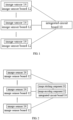
- FIG. 1 is a structural block diagram of a camera according to an optional embodiment of the present application.
- the camera can include: an integrated circuit board 10, and a plurality of image sensor boards 12, each of the a plurality of image sensor boards 12 has an image sensor 14 mounted thereon.
- the image sensor boards 12 are configured for outputting acquired first image signals to the integrated circuit board 10.
- the integrated circuit board 10 is connected with the plurality of image sensor boards 12 and configured for performing stitching and encoding processing on the first image signals.
- a camera which includes: an integrated circuit board according to claims 1 or 2, and a plurality of image sensor boards, each of the image sensor boards has an image sensor mounted thereon; the plurality of image sensor boards are configured for outputting acquired first image signals to the integrated circuit board; and the integrated circuit board is connected with the plurality of image sensor boards and configured for performing stitching and encoding processing on the first image signals.
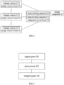
- FIG. 2 is a first structural block diagram of a camera according to an optional embodiment of the present application.
- the integrated circuit board 10 described above further includes: an image stitching component 20 and an image encoding component 22 as specifically described below.
- the image stitching component 20 is configured for outputting second image signals, which are obtained by performing stitching processing on the first image signals, to the image encoding component 22.
- the first image signals are image signals acquired by the image sensors 10
- the second image signals are image signals processed by the image stitching component 20
- third image signals are image signals processed by the image encoding component 22.
- the image stitching component 20 can be implemented with a Field-Programmable Gate Array (FPGA) chip.
- the FPGA chips with different specifications may be selected according to the strength of signals acquired by the image sensors 14.
- an FPGA chip of XC7A200T may be used, which can provide an overall image signal with a resolution of 4096 * 1800 after performing stitching processing for the image signals acquired by four IMX185 image sensors.
- the image encoding component 22 is connected with the image stitching component 20 and configured for outputting third image signals which are obtained by encoding the second image signals.
- the encoding process in the image encoding component 22 includes performing such as analog-digital conversion, format conversion, and compression on the image signals subjected to the stitching processing.
- the image encoding component 22 can be implemented with a Digital Signal Processor (DSP).
- DSP Digital Signal Processor
- the DSP is based on the AMBARELLA DSP platform, the clock rate of the dual core Cortex-A9 integrated therein is up to 1.1GHz, which can implement encoding with 1080P, 120 frames.
- the description here is only for this specific embodiment, other platform's chips, such as a Hi3516A chip, can also be used to encode the images.
- the image encoding component 22 is further configured for sending a control signal to the image stitching component 20 and/or reading a current operation state of the image stitching component via Serial Peripheral Interfaces (SPIs), wherein the control signal is used for controlling or instructing the image stitching component 20 to perform stitching processing on the first image signals.
- SPIs Serial Peripheral Interfaces
- the SPI supports full duplex communication, which further facilitates the information interaction between the image stitching component 20 and the image encoding component 22.
- the half duplex or simplex communication can be used between the image stitching component 20 and the image encoding component 22 in this embodiment.
- the image stitching component 20 is configured for outputting the second image signals to the image encoding component 22 via at least one pair of differential clock signal lines and twelve pairs of differential data signal lines.
- each of the image sensors sends the contents in acquired image signals to the image stitching component 20 (e.g. an FPGA chip) via four pairs of differential data signal lines, and at the same time, a pair of differential clock signal lines is needed to ensure that the image signals sent to the image stitching component 20 are synchronized in time, such that the connected four image sensors operate in synchronous mode.
- the image stitching component 20 implements seamless stitching processing on four image signals by processing the synchronized image signals from the four image sensors.
- the image stitching component 20 outputs at least one pair of differential clock signals and twelve pairs of differential data signals to the image encoding component 22 by using at least one pair of differential clock signal lines and twelve pairs of differential data signal lines.
- the differential clock signal lines are used for transmitting clock signals, and the differential data signal lines are used for transmitting data signals.
- Each pair of signal lines can include two transmission channels.
- one of the two transmission channels of one pair of signal lines is used for transmitting the code "0" and the other is used for transmitting the code "1".
- the twelve pairs of differential data signals derive from 16 differential data signals acquired by the 4 image sensors, and at least one pair of differential clock signals derives from 4 pairs of clock signals of the image sensors. In a good communication environment, it only needs to transmit one clock signal; while in a poor communication environment, it needs to transmit two clock signals of main and standby clock signals, so as to ensure the receipt of the clock signal.
- the image stitching component 20 is connected with the image encoding component 22 via two pairs of differential clock signal lines and twelve pairs of differential data signal lines.
- the image stitching component 20 in the camera according to this embodiment is further configured for configuring the image sensor 14 on each of the image sensor boards 12 and/or reading a current operation state of the image sensor 14 via serial peripheral interfaces.
- interfaces in half duplex or simplex communication can be used to connect the image stitching component 20 and the image sensor boards 12.
- FIG. 3 is a second structural block diagram of a camera according to an optional embodiment of the present application.
- the camera can further include one or more storage components 30, which are connected with the integrated circuit board 10 and configured for storing first image signals.
- the camera can further include the storage component 30 for storing image signals input by the image sensors 14.
- the storage component 30 can store image signals respectively.
- one storage may be divided into four storage divisions for storing image signals acquired by the four image sensors 14 respectively.
- 4 independent storage components 30 can be provided, each is connected with each of the image sensors 14 or connected with the image stitching component 20 in the integrated circuit board 10, and configured for storing image signals acquired by each of the image sensors 14 respectively.
- the image stitching component 20 is externally connected with 4 Double Data Rate synchronous dynamic random storages (DDRs for short), each with 16 bits wide and with a capacity of 1GB.
- DDRs Double Data Rate synchronous dynamic random storages
- the integrated circuit board 10 is connected with a plurality of image sensor boards 12 via board-to-board flexible connecting lines.
- the image sensor boards 12 mainly implement the acquiring of image signals.
- the signals transmitted via the flexible connecting lines include image signals, power and SPI communication signals, and other control signals.
- the image sensor boards 12 are connected with the integrated circuit board 10 via four 1.0-pitch and 30-bit board-to-board flexible connecting lines.
- the shape of a photosensitive surface of an image sensor on each of the image sensor boards 12 is a rectangle, and short edges of the rectangle are parallel to the ground plane and long edges of the rectangle are perpendicular to the ground plane.
- Outer surfaces of the image sensors on the plurality of image sensor boards form a sector with a preset angle.
- each image sensor 14 is mounted on an image sensor board 12.
- the photosensitive surface of the surface of the image sensor 14 is a sheet with a rectangular shape, and short edges of the rectangle are parallel to the ground plane and long edges of the rectangle are perpendicular to the ground plane.
- Outer surfaces of the plurality of image sensors 14 form a sector.
- the extension lines of the normal lines of the outer surfaces of the plurality of image sensors can intersect at a same point, such that the outer surfaces of the image sensors 14 form a sector with 180 degree or other angle.
- Each of the image sensors 14 are arranged at a regular interval along the curve of the sector. The angle of the sector can be adjusted according to the number of the image sensors 14.
- each of the sensors is mounted in such a way that the sensor is centered at the screen center and rotated by 90 degrees. 4 sensors are fixed on a single apparatus with their glass surfaces outward forming a sector with 180 degree.
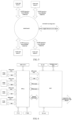
- FIG. 4 is a structural block diagram of an integrated circuit board according to an optional embodiment of the present application.
- the integrated circuit board can be applied in the camera described above, and can also be mounted and applied in other apparatus.
- the integrated circuit board can include: an input port 40, a processor 42 and an output port 44 as described in detail below.
- the input port 40 is connected with a plurality of image sensor boards and configured for receiving an image signal acquired by an image sensor mounted on each of the plurality of image sensor boards.
- the image sensor can be an IMX185 image sensor that is widely used in the industry, and the resolution of 1920 * 1200 can be provided by a single image sensor.
- the image sensor boards are connected with the integrated circuit board via board-to-board flexible connecting lines, such as the board-to-board flexible with the standards of: a 1.0-pitch and 30-bit, which transmits image signals and other control signals.
- the processor 42 is connected with the input port and configured for performing stitching and encoding processing on the image signals.
- the processor 42 can simultaneously perform stitching and encoding processing on the received image signals acquired by a plurality of image sensors, or firstly perform stitching processing and then encode the image signals, or firstly perform encode processing and then perform stitching processing on the image signals.
- the stitching processing is firstly performed on image signals, and then the image signals subjected to the stitching processing are encoded.
- the output port 44 is connected with the processor 42 and configured for outputting the image signals subjected to the stitching and encoding processing.
- the output port 44 can output the image signals processed by the processor 42 to an external display apparatus, a server or the like, by specifically reserving wires for ports, such as alarm inputs and outputs, audio inputs and outputs, 485-interfaces as well as power and network interfaces.
- the input port 40 is configured for receiving image signals via a pair of differential clock signal lines and a plurality pairs of differential data signal lines.
- the number of the image sensor boards is 4.
- An image sensor transmits acquired image signals via a pair of differential clock signal lines and 4 pairs of differential data signal lines.
- the differential clock signal lines are used for ensuring that the image signals output by different image sensors are synchronized in time, and the differential data signal lines are used for transmitting the contents in the image signals.
- each of the image sensor boards can further include, but not limited to, the following components (not shown in the figure): a power circuit and a socket.
- the integrated circuit board can further include, but not limited to, the following components (not shown in the figure): a power supply component (such as, a power supply for the integrated circuit board), a power interface circuit, a power conversion circuit.
- the power supply component can be powered by a Power over Ethernet (POE) component.
- the power interface can be a DC or an AC interface circuit, such as an AC24 or DC 12V interface circuit.
- FIG. 5 is a schematic diagram of the internal structure of a camera according to an optional embodiment of the present application.
- the camera can include: a main board (equivalent to the integrated circuit board in the above embodiment), front-end boards (equivalent to the image sensor boards in the above embodiment), and connecting components.
- the modules in hardware implementation of the camera in this embodiment involve the following portions.
- the image sensors can be IMX185 image sensors widely used in the industry.
- the resolution of 1920 * 1200 can be provided by one single image sensor, the resolution of 4096 * 1800 can be provided by stitching the images from the four sensors .
- the FPGA chip XC7A200T is employed, 4 DDRs, each with 16 bits of a bit wide and 1GB of the capacity, are connected externally.
- the DSP is based on the AMBARELLA DSP platform, the clock rate of the dual core Cortex-A9 internally integrated is up to 1.1GHz, which can implement encoding at 1080P at 120 frames per second.
- the camera of this embodiment is connected with 4 sensors.
- An FPGA in larger package can be used to connect with more sensors.
- FIG. 5 is a structural block diagram of an optional embodiment.
- the main board of this embodiment includes an FPGA module circuit, a DSP module circuit, as well as a POE and an AC24, a DC12V interface circuit, a system power conversion circuit.
- the front-end boards are connected with the main board via four 1.0-pitch and 30-bit board-to-board flexible connecting lines.
- the main board reserves wires for external interfaces, such as alarm inputs and outputs, audio inputs and outputs, 485-interfaces as well as power and network interfaces.
- FIG. 6 is a schematic diagram for performing stitching and encoding processing on an image signal according to an optional embodiment of the present application.
- the main board accesses to four image sensors by XC7A200T chip.
- Each of the sensors is connected with the FPGA chip via four pairs of differential data signal lines and a pair of differential clock signal lines.
- the XC7A200T is mainly used to ensure that the four accessed image sensors operate in synchronous mode.
- the FPGA is connected with image interfaces of the DSP main chip via twelve pairs of differential data signal lines and 2 pairs of differential clock signal lines.
- the DSP module is mainly used for encoding front-end image signals and controlling peripherals.
- the DSP module communicates with the FPGA via an SPI, and an I2C is reserved for communication for configuring the sensors.
- the DSP module communicates with a microcontroller via the I2C.
- the system uses an STM8 microcontroller and heating logic to control a heating module and a fan in order to achieve the function of the heating module.
- the main board can be powered by POE and a DC 12V power supply, the function of being powered by an AC24V power supply is optional.
- the 12V power is converted to 5V power by a DCDC chip, and then the 5V power is converted to appropriate power required by other modules.
- the front-end boards mainly implement the acquiring of image signals.
- the front-end boards are connected with the main board via 1.0-pitch and 30-bit board-to-board flexible connecting lines, in order to implement transmission of the image signals, SPI communication signals and other control signals, and to provide power.
- Each of the sensors is mounted on a sensor circuit board.
- the sensor is a sheet with a rectangular shape.
- Each of the sensors is mounted in such a way that the sensor is rotated by 90 degrees taking the screen center as the origin point, and its short edges are parallel to the ground plane and long edges are perpendicular to the ground plane.
- the 4 sensors are fixed on a single apparatus with their glass surfaces outward forming a sector with 180 degree.
- Each of the sensors is connected with each other via 1.0 pitch and 30-bit board-to-board flexible connecting lines.
- Each of the sensors is connected with the FPGA chip via 4 pairs of differential data signal lines and 1 pair of differential clock signal lines.
- the FPGA can configure the sensors via SPIs.
- the FPGA is connected with DDR chips via wires inside the board.
- the FPGA is further connected with test components, such as a Joint Test Action Group (JTAG for short), for joint testing for FPGA.
- JTAG Joint Test Action Group
- the FPGA is connected with an image processing chip via wires inside the board.
- the FPGA outputs the stitched images to the image processing chip via a set of image data interfaces.
- the FPGA interacts with the image processing chip to exchange control information via a set of SPIs.
- the disclosed technical solution can be implemented in other ways.
- the apparatus embodiments described above are merely illustrative.
- the apparatus can be divided into units according to the logical functions, however, in practice, the apparatus can be divided in other ways.
- a plurality of units or components can be combined or integrated into another system, or some features can be ignored or not executed.
- the coupling or direct coupling or communication connections between each other shown or discussed above can be indirect coupling or communication connections via the interfaces, units or modules, which can be electrical connections or other forms of connections.
- the units illustrated as separate components may or may not be physically separated.
- the components shown as units may or may not be physical units, and can be located on one unit or can be distributed on a plurality of units. Some or all of the units can be selected according to actual needs to achieve the objective of the solution of the present embodiments.
- all the functional units in the embodiments of the present application can be integrated in one processing unit, or each of the units can be an individual unit, or two or more units can be integrated in one unit.
- the integrated unit described above can be implemented as hardware or can be implemented as a software function unit.
- the integrated unit When the integrated unit is implemented as a software function unit and is sold or used as an independent product, the integrated unit can be stored in a computer readable storage medium.
- the computer software product is stored in a storage medium, including instructions to make a computer device (such as, a personal computer, a server or network equipment) perform all or some of the steps of the method of each embodiment of the present application.
- the storage medium includes medium capable of storing program code, such as a USB flash disk, a Read Only Memory (ROM), a Random Access Memory (RAM), a mobile hard disk, a magnetic disk, or an optical disk.
Landscapes
- Engineering & Computer Science (AREA)
- Multimedia (AREA)
- Signal Processing (AREA)
- Human Computer Interaction (AREA)
- Studio Devices (AREA)
Description
- The present application claims the priority to a
Chinese patent application No. 201520530956.2 filed with the State Intellectual Property Office of People's Republic of China on July 21, 2015 - The application relates to the field of video monitoring, in particular to a camera and an integrated circuit board.
- A camera is an important component for a monitoring system. Due to limitations of the lens shooting angle, the common single-lens cameras available from the market can only shoot scenes from relatively small angles. Due to the shooting angle of the camera, pictures can only be taken at a small angle, with a small view angle and more blind spots, and thus it is unable to meet the needs of large-scale outdoor monitoring, such as monitoring of large roads, bridges, squares, roofs, or the like.
- In the prior art, a video monitoring camera includes an image sensor for acquiring images, an image processor for encoding and performing analog-to-digital conversion on the images acquired by the image sensors, communication transmission lines and power transmission lines. Some video monitoring cameras further include a server for performing post-processing and integration on the images encoded by video monitoring cameras, so that the pictures shot are presented with a certain angle and quality when being displayed in a back-end.
- Multi-lens panoramic cameras can avoid the drawbacks of single-lens cameras in monitoring. A conventional video monitoring camera can only receive images from one image sensor, and its monitoring range is generally less than 150 degrees of a view angle. In order to achieve monitoring within 180 degrees in horizontal, it is necessary to place additional monitoring cameras to coverage a greater view angle and to stitch images acquired by a plurality of cameras by a server, which results in high equipment costs. For the case that images acquired by a plurality of cameras are stitched into one image, the cameras should be placed strictly in a certain angle according to standards, otherwise it will seriously affect the effect of stitching, which increases the difficulty in installation and testing on site.
- No effective solution has been proposed so far to solve the above problem.
-
CN 102137229A relates to the technical fields of broadcast television and monitoring, in particular relates to an embedded high-definition panoramic camera and a method thereof. The camera comprises a sensing and acquiring module, a master control circuit and a transmission module, and is characterized in that a spherical shell is provided with multipath sensors; each path of sensor is provided with signal wires which are connected with input ends of charge coupled device (CCD) acquisition modules; signal wires of the output end of a differential signal processing module are connected to the differential receiver end of the master control module by network cables; and the output end of the master control module is connected with a video compression module chip and static image module signal wires, wherein the video compression module chip and the static image module signal wires are connected with signal wires of a Gigabit network transmission module. A brand-new design architecture of the panoramic camera is adopted, and an advanced short-distance transmission technology is applied to a panoramic camera system, thus realizing 360-degree panoramic images of the camera; and an image preprocessing technology, a vide postprocessing technology, a low-power consumption design and other technologies are combined, thus ensuring the high definition and instantaneity of the panoramic images. -
US 2007126863A1 discloses a stereoscopic imaging system, which incorporates a plurality of imaging devices or cameras to generate a high resolution,
wide field of view image database from which images can be combined in real time to provide wide field of view or panoramic or omni-directional still or video images. -
US 2015009350A1 relates to a method of outputting multiple views from a networked camera. Each imager of an array of imagers in the camera captures image frames and transmits the captured image frames to an associated image flow processor. Each image flow processor processes the captured image frames and transmits the processed image frames to a multi-imager video processor. An updating of parameters for said processing by each image flow processor is performed on a frame-by-frame basis.US 2015009350A1 also relates to a video camera including a plurality of imagers, a plurality of image flow processors, a multi-imager video processor, and a plurality of update queues. -
US 2014266773A1 provids a method for a system including a plurality of remote sensor apparatus and a portable receiver. The portable receiver includes an RFID reader. The remote sensor apparatus has an RFID unit. The method includes reading RFID stored in the RFID unit of one or more of the plurality of remote sensor apparatus using the RFID reader. The method also includes registering the one or more of the plurality of remote sensor apparatus using the received RFID. The method further includes receiving data from a first active remote sensor apparatus. The data includes sensor data collected from sensors installed in the first active remote sensor and RFID of the first active remote sensor apparatus. The method also includes processing the sensor data, if the RFID of the first active remote sensor apparatus matches the RFID of any of the one or more of the plurality of remote sensor apparatus. - Embodiments of the present application provide a camera and an integrated circuit board, in order to at least solve the technical problem that it is difficult for camera equipment provided in the prior art to achieve panoramic shooting.
- The present application provides a camera, which includes: an integrated circuit board and a plurality of image sensor boards, wherein each of the image sensor boards has an image sensor mounted thereon; the plurality of image sensor boards are configured for outputting acquired first image signals to the integrated circuit board; and the integrated circuit board is connected with the plurality of image sensor boards and configured for performing stitching and encoding processing on the first image signals.
- Further, the integrated circuit board includes: an image stitching component configured for outputting second image signals, which are obtained by performing stitching processing on the first image signals, to an image encoding component; and the image encoding component connected with the image stitching component and configured for outputting third image signals which are obtained by performing encoding processing on the second image signals.
- Further, the image encoding component is further configured for sending a control signal to the image stitching component and/or reading a current operation state of the image stitching component via serial peripheral interfaces.
- Further, the image stitching component is configured for outputting the second image signals to the image encoding component via at least one pair of differential clock signal lines and twelve pairs of differential data signal lines.
- Further, the image stitching component is further configured for configuring the image sensor on each of the image sensor boards and/or reading a current operation state of the image sensor via serial peripheral interfaces.
- Further, the camera further includes one or more storage components connected with the integrated circuit board and configured for storing the first image signals.
- Further, the integrated circuit board is connected with the plurality of image sensor boards via flexible connecting lines.
- Further, the shape of a photosensitive surface of an image sensor on each of the image sensor boards is a rectangle, short edges of the rectangle are parallel to the ground plane and long edges of the rectangle are perpendicular to the ground plane, and outer surfaces of the image sensors on the plurality of image sensor boards form a sector with a preset angle.
- The present application further provides an integrated circuit board, which includes: an input port, connected with a plurality of image sensor boards and configured for receiving an image signal acquired by an image sensor mounted on each of the plurality of image sensor boards; a processor, connected with the input port and configured for performing stitching and encoding processing on the image signals; and an output port, connected with the processor and configured for outputting image signals subjected to the stitching and encoding processing.
- Further, the input port is configured for receiving the image signals via a pair of differential clock signal lines and a plurality of pairs of differential data signal lines.
- The embodiments of the present application provide an integrated circuit board according to
claim 1 and a camera according to claim 3 comprising said integrated circuit board. - The drawings described herein are used to provide further understanding of the present application, and form a part of the present application. The schematic embodiments and description herein are used to explain the present application and do not constitute improper limitations to the present application. In the drawings:
-
FIG. 1 is a structural block diagram of a camera according to an optional embodiment of the present application; -
FIG. 2 is a first structural block diagram of a camera according to an optional embodiment of the present application; -
FIG. 3 is a second structural block diagram of a camera according to an optional embodiment of the present application; -
FIG. 4 is a structural block diagram of an integrated circuit board according to an optional embodiment of the present application; -
FIG. 5 is a schematic diagram of the internal structure of a camera according to an optional embodiment of the present application; -
FIG. 6 is a schematic diagram for performing stitching and encoding processing on an image signal according to an optional embodiment of the present application; - The reference signs in the drawings described above are provided as follows: 10. integrated circuit board; 12. image sensor board; 14. image sensor; 20. image stitching component; 22. image encoding component; 30. storage component; 40. input port; 42. processor; 44. output port.
- In order to make those of ordinary skills in the art better understand the solution of the present application, the technical solution of the present application will be described in detail with reference to the drawings of embodiments of the present application. Obviously, the embodiments described are merely some of the embodiments of the present application, instead of all the embodiments.
- It should be noted that the terms such as "first", "second" and the like in the description and claims of the present application and in the drawings described above are used to distinguish similar objects, and are not necessarily used to describe a specific order or sequence. It should be understood that the data used in this way are interchangeable under appropriate circumstances so that the embodiments of the present application described herein can be implemented in an order other than those illustrated or described herein. Moreover, the terms "include", "comprise" and "have" or any variants thereof are intended to cover non-exclusive inclusions. For example, processes, methods, systems, products or devices including a series of steps or elements include not only those steps or elements specifically listed but also those not specifically listed or intrinsic to such processes, methods, systems, products or devices.
- A camera is provided according to an embodiment of the present application. It should be noted that steps shown in the flowcharts of the drawings can be performed in a computer system, such as a computer system that can execute a set of computer-executable instructions. Although a logical order is shown in a flowchart, in some cases, the steps shown or described can be performed in an order different from the logical order herein.
-
FIG. 1 is a structural block diagram of a camera according to an optional embodiment of the present application. As shown inFIG. 1 , the camera can include: anintegrated circuit board 10, and a plurality ofimage sensor boards 12, each of the a plurality ofimage sensor boards 12 has animage sensor 14 mounted thereon. - The
image sensor boards 12 are configured for outputting acquired first image signals to the integratedcircuit board 10. - The
integrated circuit board 10 is connected with the plurality ofimage sensor boards 12 and configured for performing stitching and encoding processing on the first image signals. - In the embodiment of the present application, a camera is provided, which includes: an integrated circuit board according to
claims -
FIG. 2 is a first structural block diagram of a camera according to an optional embodiment of the present application. As shown inFIG. 2 , on the basis of the structural block diagram of the camera shown inFIG. 1 , theintegrated circuit board 10 described above further includes: animage stitching component 20 and animage encoding component 22 as specifically described below. - The
image stitching component 20 is configured for outputting second image signals, which are obtained by performing stitching processing on the first image signals, to theimage encoding component 22. - In this embodiment, the first image signals are image signals acquired by the
image sensors 10, the second image signals are image signals processed by theimage stitching component 20, and third image signals are image signals processed by theimage encoding component 22. Specifically, theimage stitching component 20 can be implemented with a Field-Programmable Gate Array (FPGA) chip. The FPGA chips with different specifications may be selected according to the strength of signals acquired by theimage sensors 14. In a preferred embodiment, an FPGA chip of XC7A200T may be used, which can provide an overall image signal with a resolution of 4096 * 1800 after performing stitching processing for the image signals acquired by four IMX185 image sensors. - The
image encoding component 22 is connected with theimage stitching component 20 and configured for outputting third image signals which are obtained by encoding the second image signals. - Optionally, the encoding process in the
image encoding component 22 includes performing such as analog-digital conversion, format conversion, and compression on the image signals subjected to the stitching processing. Theimage encoding component 22 can be implemented with a Digital Signal Processor (DSP). In this embodiment, the DSP is based on the AMBARELLA DSP platform, the clock rate of the dual core Cortex-A9 integrated therein is up to 1.1GHz, which can implement encoding with 1080P, 120 frames. The description here is only for this specific embodiment, other platform's chips, such as a Hi3516A chip, can also be used to encode the images. - In an optional implementation according to this embodiment, the
image encoding component 22 is further configured for sending a control signal to theimage stitching component 20 and/or reading a current operation state of the image stitching component via Serial Peripheral Interfaces (SPIs), wherein the control signal is used for controlling or instructing theimage stitching component 20 to perform stitching processing on the first image signals. The SPI supports full duplex communication, which further facilitates the information interaction between theimage stitching component 20 and theimage encoding component 22. However, the half duplex or simplex communication can be used between theimage stitching component 20 and theimage encoding component 22 in this embodiment. - In an implementation according to this embodiment, the
image stitching component 20 is configured for outputting the second image signals to theimage encoding component 22 via at least one pair of differential clock signal lines and twelve pairs of differential data signal lines. - In this embodiment, each of the image sensors sends the contents in acquired image signals to the image stitching component 20 (e.g. an FPGA chip) via four pairs of differential data signal lines, and at the same time, a pair of differential clock signal lines is needed to ensure that the image signals sent to the
image stitching component 20 are synchronized in time, such that the connected four image sensors operate in synchronous mode. Theimage stitching component 20 implements seamless stitching processing on four image signals by processing the synchronized image signals from the four image sensors. Theimage stitching component 20 outputs at least one pair of differential clock signals and twelve pairs of differential data signals to theimage encoding component 22 by using at least one pair of differential clock signal lines and twelve pairs of differential data signal lines. The differential clock signal lines are used for transmitting clock signals, and the differential data signal lines are used for transmitting data signals. Each pair of signal lines can include two transmission channels. In an optional example, for transmission of binary data signals, one of the two transmission channels of one pair of signal lines is used for transmitting the code "0" and the other is used for transmitting the code "1". The twelve pairs of differential data signals derive from 16 differential data signals acquired by the 4 image sensors, and at least one pair of differential clock signals derives from 4 pairs of clock signals of the image sensors. In a good communication environment, it only needs to transmit one clock signal; while in a poor communication environment, it needs to transmit two clock signals of main and standby clock signals, so as to ensure the receipt of the clock signal. In an optional example of this embodiment, theimage stitching component 20 is connected with theimage encoding component 22 via two pairs of differential clock signal lines and twelve pairs of differential data signal lines. - In an optional implementation of this embodiment, the
image stitching component 20 in the camera according to this embodiment is further configured for configuring theimage sensor 14 on each of theimage sensor boards 12 and/or reading a current operation state of theimage sensor 14 via serial peripheral interfaces. However, in this embodiment, interfaces in half duplex or simplex communication can be used to connect theimage stitching component 20 and theimage sensor boards 12. -
FIG. 3 is a second structural block diagram of a camera according to an optional embodiment of the present application. As shown inFIG. 3 , on the basis of components shown inFIG. 2 , the camera can further include one ormore storage components 30, which are connected with theintegrated circuit board 10 and configured for storing first image signals. - In this embodiment, the camera can further include the
storage component 30 for storing image signals input by theimage sensors 14. Optionally, in an example of using four image sensors for acquiring the image signal, thestorage component 30 can store image signals respectively. For example, one storage may be divided into four storage divisions for storing image signals acquired by the fourimage sensors 14 respectively. Also, 4independent storage components 30 can be provided, each is connected with each of theimage sensors 14 or connected with theimage stitching component 20 in the integratedcircuit board 10, and configured for storing image signals acquired by each of theimage sensors 14 respectively. In a specific implementation, theimage stitching component 20 is externally connected with 4 Double Data Rate synchronous dynamic random storages (DDRs for short), each with 16 bits wide and with a capacity of 1GB. - In an optional implementation of this embodiment, the
integrated circuit board 10 is connected with a plurality ofimage sensor boards 12 via board-to-board flexible connecting lines. In this optional implementation, theimage sensor boards 12 mainly implement the acquiring of image signals. The signals transmitted via the flexible connecting lines include image signals, power and SPI communication signals, and other control signals. In a specific example, theimage sensor boards 12 are connected with theintegrated circuit board 10 via four 1.0-pitch and 30-bit board-to-board flexible connecting lines. - In an optional implementation of this embodiment, the shape of a photosensitive surface of an image sensor on each of the
image sensor boards 12 is a rectangle, and short edges of the rectangle are parallel to the ground plane and long edges of the rectangle are perpendicular to the ground plane. Outer surfaces of the image sensors on the plurality of image sensor boards form a sector with a preset angle. - In this embodiment, each
image sensor 14 is mounted on animage sensor board 12. The photosensitive surface of the surface of theimage sensor 14 is a sheet with a rectangular shape, and short edges of the rectangle are parallel to the ground plane and long edges of the rectangle are perpendicular to the ground plane. Outer surfaces of the plurality ofimage sensors 14 form a sector. In a preferred implementation, the extension lines of the normal lines of the outer surfaces of the plurality of image sensors can intersect at a same point, such that the outer surfaces of theimage sensors 14 form a sector with 180 degree or other angle. Each of theimage sensors 14 are arranged at a regular interval along the curve of the sector. The angle of the sector can be adjusted according to the number of theimage sensors 14. In a specific example, each of the sensors is mounted in such a way that the sensor is centered at the screen center and rotated by 90 degrees. 4 sensors are fixed on a single apparatus with their glass surfaces outward forming a sector with 180 degree. -
FIG. 4 is a structural block diagram of an integrated circuit board according to an optional embodiment of the present application. The integrated circuit board can be applied in the camera described above, and can also be mounted and applied in other apparatus. As shown inFIG. 4 , the integrated circuit board can include: aninput port 40, aprocessor 42 and anoutput port 44 as described in detail below. - The
input port 40 is connected with a plurality of image sensor boards and configured for receiving an image signal acquired by an image sensor mounted on each of the plurality of image sensor boards. - It should be noted that, in practice, the image sensor can be an IMX185 image sensor that is widely used in the industry, and the resolution of 1920 * 1200 can be provided by a single image sensor. Optionally, the image sensor boards are connected with the integrated circuit board via board-to-board flexible connecting lines, such as the board-to-board flexible with the standards of: a 1.0-pitch and 30-bit, which transmits image signals and other control signals.
- The
processor 42 is connected with the input port and configured for performing stitching and encoding processing on the image signals. - Optionally, the
processor 42 can simultaneously perform stitching and encoding processing on the received image signals acquired by a plurality of image sensors, or firstly perform stitching processing and then encode the image signals, or firstly perform encode processing and then perform stitching processing on the image signals. In the embodiment of the invention, the stitching processing is firstly performed on image signals, and then the image signals subjected to the stitching processing are encoded. - The
output port 44 is connected with theprocessor 42 and configured for outputting the image signals subjected to the stitching and encoding processing. - Optionally, the
output port 44 can output the image signals processed by theprocessor 42 to an external display apparatus, a server or the like, by specifically reserving wires for ports, such as alarm inputs and outputs, audio inputs and outputs, 485-interfaces as well as power and network interfaces. - In an optional implementation according to this embodiment, the
input port 40 is configured for receiving image signals via a pair of differential clock signal lines and a plurality pairs of differential data signal lines. - In this embodiment, the number of the image sensor boards is 4. An image sensor transmits acquired image signals via a pair of differential clock signal lines and 4 pairs of differential data signal lines. The differential clock signal lines are used for ensuring that the image signals output by different image sensors are synchronized in time, and the differential data signal lines are used for transmitting the contents in the image signals.
- Optionally, in this embodiment, one image sensor is mounted on each of the image sensor boards. Optionally, in addition to the image sensor, each of the image sensor boards can further include, but not limited to, the following components (not shown in the figure): a power circuit and a socket.
- Optionally, in addition to the
input port 40, theprocessor 42 and theoutput port 44 described above, the integrated circuit board can further include, but not limited to, the following components (not shown in the figure): a power supply component (such as, a power supply for the integrated circuit board), a power interface circuit, a power conversion circuit. The power supply component can be powered by a Power over Ethernet (POE) component. The power interface can be a DC or an AC interface circuit, such as an AC24 or DC 12V interface circuit. - The present application is specifically described below with reference to an optional embodiment.
FIG. 5 is a schematic diagram of the internal structure of a camera according to an optional embodiment of the present application. As shown inFIG. 5 , the camera can include: a main board (equivalent to the integrated circuit board in the above embodiment), front-end boards (equivalent to the image sensor boards in the above embodiment), and connecting components. The modules in hardware implementation of the camera in this embodiment involve the following portions. - For acquiring and outputting of images by image sensors, simultaneous access to four image sensors is supported. The image sensors can be IMX185 image sensors widely used in the industry. The resolution of 1920 * 1200 can be provided by one single image sensor, the resolution of 4096 * 1800 can be provided by stitching the images from the four sensors . With respect to the access processing for four-path images, the FPGA chip XC7A200T is employed, 4 DDRs, each with 16 bits of a bit wide and 1GB of the capacity, are connected externally. The DSP is based on the AMBARELLA DSP platform, the clock rate of the dual core Cortex-A9 internally integrated is up to 1.1GHz, which can implement encoding at 1080P at 120 frames per second. There are two schemes of the chip for processing the images: one is AMBARELLA DSP88, the other is Hi3516A.
- The camera of this embodiment is connected with 4 sensors. However, An FPGA in larger package can be used to connect with more sensors.
- The hardware is composed of a main board and 4 front-end boards.
FIG. 5 is a structural block diagram of an optional embodiment. As shown inFIG. 5 , the main board of this embodiment includes an FPGA module circuit, a DSP module circuit, as well as a POE and an AC24, a DC12V interface circuit, a system power conversion circuit. There are four front-end boards and each includes an image sensor module, a power supply circuit and an ICR socket. The front-end boards are connected with the main board via four 1.0-pitch and 30-bit board-to-board flexible connecting lines. The main board reserves wires for external interfaces, such as alarm inputs and outputs, audio inputs and outputs, 485-interfaces as well as power and network interfaces. -
FIG. 6 is a schematic diagram for performing stitching and encoding processing on an image signal according to an optional embodiment of the present application. As shown inFIG. 6 , the main board accesses to four image sensors by XC7A200T chip. Each of the sensors is connected with the FPGA chip via four pairs of differential data signal lines and a pair of differential clock signal lines. The XC7A200T is mainly used to ensure that the four accessed image sensors operate in synchronous mode. The FPGA is connected with image interfaces of the DSP main chip via twelve pairs of differential data signal lines and 2 pairs of differential clock signal lines. - The DSP module is mainly used for encoding front-end image signals and controlling peripherals. The DSP module communicates with the FPGA via an SPI, and an I2C is reserved for communication for configuring the sensors. The DSP module communicates with a microcontroller via the I2C. The system uses an STM8 microcontroller and heating logic to control a heating module and a fan in order to achieve the function of the heating module. The main board can be powered by POE and a DC 12V power supply, the function of being powered by an AC24V power supply is optional. The 12V power is converted to 5V power by a DCDC chip, and then the 5V power is converted to appropriate power required by other modules.
- The front-end boards mainly implement the acquiring of image signals. The front-end boards are connected with the main board via 1.0-pitch and 30-bit board-to-board flexible connecting lines, in order to implement transmission of the image signals, SPI communication signals and other control signals, and to provide power.
- Each of the sensors is mounted on a sensor circuit board. The sensor is a sheet with a rectangular shape. Each of the sensors is mounted in such a way that the sensor is rotated by 90 degrees taking the screen center as the origin point, and its short edges are parallel to the ground plane and long edges are perpendicular to the ground plane. The 4 sensors are fixed on a single apparatus with their glass surfaces outward forming a sector with 180 degree.
- Each of the sensors is connected with each other via 1.0 pitch and 30-bit board-to-board flexible connecting lines. Each of the sensors is connected with the FPGA chip via 4 pairs of differential data signal lines and 1 pair of differential clock signal lines. In addition, the FPGA can configure the sensors via SPIs.
- The FPGA is connected with DDR chips via wires inside the board. The FPGA is further connected with test components, such as a Joint Test Action Group (JTAG for short), for joint testing for FPGA.
- The FPGA is connected with an image processing chip via wires inside the board. The FPGA outputs the stitched images to the image processing chip via a set of image data interfaces. The FPGA interacts with the image processing chip to exchange control information via a set of SPIs.
- The serial numbers of the above embodiments of the present application, if any, are merely for description and do not indicate that one embodiment is better than another.
- For the description of each of the embodiments of the present application, the emphasis is laid on a particular aspect. For the parts that are not described in detail in a certain embodiment, references can be made to the related description of other embodiments.
- It should be understood that in the embodiments herein, the disclosed technical solution can be implemented in other ways. The apparatus embodiments described above are merely illustrative. For example, the apparatus can be divided into units according to the logical functions, however, in practice, the apparatus can be divided in other ways. For example, a plurality of units or components can be combined or integrated into another system, or some features can be ignored or not executed. Further, the coupling or direct coupling or communication connections between each other shown or discussed above can be indirect coupling or communication connections via the interfaces, units or modules, which can be electrical connections or other forms of connections.
- The units illustrated as separate components may or may not be physically separated. The components shown as units may or may not be physical units, and can be located on one unit or can be distributed on a plurality of units. Some or all of the units can be selected according to actual needs to achieve the objective of the solution of the present embodiments.
- In addition, all the functional units in the embodiments of the present application can be integrated in one processing unit, or each of the units can be an individual unit, or two or more units can be integrated in one unit. The integrated unit described above can be implemented as hardware or can be implemented as a software function unit.
- When the integrated unit is implemented as a software function unit and is sold or used as an independent product, the integrated unit can be stored in a computer readable storage medium. On the basis of the understanding above, the essential technical solution of the present application, or the part contributing to the prior art, or all or a part of the technical solution can be implemented as a software product. The computer software product is stored in a storage medium, including instructions to make a computer device (such as, a personal computer, a server or network equipment) perform all or some of the steps of the method of each embodiment of the present application. The storage medium includes medium capable of storing program code, such as a USB flash disk, a Read Only Memory (ROM), a Random Access Memory (RAM), a mobile hard disk, a magnetic disk, or an optical disk.
- The implementations are merely preferred implementations of the invention defined by the appended claims.
Claims (7)
- An integrated circuit board (10), comprising:an input port, connected with a plurality of image sensor boards (12) and configured for receiving first image signals acquired by an image sensor (14) mounted on each of the plurality of image sensor boards (12);a processor, connected with the input port and configured for performing stitching and encoding processing on the image signals by using an image stitching component (20) and an image encoding component (22); andan output port, connected with the processor and configured for outputting image signals subjected to the stitching and encoding processing;wherein the image stitching component (20) is configured for outputting second image signals, which are obtained by performing stitching processing on the first image signals, to an image encoding component (22);- wherein the image encoding component (22) is connected with the image stitching component (20) and configured for outputting third image signals which are obtained by performing encoding processing on the second image signals;- wherein the image encoding component (22) is further configured for sending a control signal to the image stitching component (20) and/or reading a current operation state of the image stitching component (20) via serial peripheral interfaces,wherein the control signal is used for controlling or instructing the image stitching component (20) to perform stitching processing on the first image signals; andwherein the image stitching component (20) is configured for outputting the second image signals to the image encoding component (22) via at least one pair of differential clock signal lines and twelve pairs of differential data signal lines; the twelve pairs of differential data signals derive from 16 differential data signals acquired by 4 image sensors (14) mounted on said plurality of image sensor boards (12), and the at least one pair of differential clock signals derives from 4 pairs of clock signals of the 4 image sensors (14).
- The integrated circuit board (10) of claim 1, wherein the input port is configured for receiving the image signals via a pair of differential clock signal lines and a plurality of pairs of differential data signal lines.
- A camera, comprising: an integrated circuit board (10) according to claim 1 or 2, and a plurality of image sensor boards (12), wherein each of the image sensor boards (12) has an image sensor (14) mounted thereon;the plurality of image sensor boards (12) are configured for outputting acquired first image signals to the integrated circuit board (10); andthe integrated circuit board (10) is connected with the plurality of image sensor boards (12) and configured for performing stitching and encoding processing on the first image signals; wherein the image stitching component (20) is configured for outputting the second image signals to the image encoding component (22) via at least one pair of differential clock signal lines and twelve pairs of differential data signal lines.
- The camera of claim 3, wherein the image stitching component (20) is further configured for reading a current operation state of the image sensor (14) via serial peripheral interfaces.
- The camera of claim 3, wherein the camera further comprises one or more storage components (30) connected with the integrated circuit board (10) and configured for storing the first image signals.
- The camera of claim 3, wherein the integrated circuit board (10) is connected with the plurality of image sensor boards (12) via flexible connecting lines.
- The camera of claim 3, wherein the shape of a photosensitive surface of an image sensor (14) on each of the image sensor boards (12) is a rectangle, short edges of the rectangle are parallel to the ground plane and long edges of the rectangle are perpendicular to the ground plane, and extension lines of normal lines of outer surfaces of the image sensors (14) intersect at a same point and the outer surfaces of the image sensors (14) on the plurality of image sensor boards (12) form a sector with a preset angle, wherein the image sensors (14) are arranged at a regular interval along the curve of the sector, and the preset angle is adjustable according to the number of the image sensors (14).
Applications Claiming Priority (2)
| Application Number | Priority Date | Filing Date | Title |
|---|---|---|---|
| CN201520530956.2U CN204993576U (en) | 2015-07-21 | 2015-07-21 | Camera and integrated circuit board |
| PCT/CN2016/081830 WO2017012396A1 (en) | 2015-07-21 | 2016-05-12 | Camera and integrated circuit board |
Publications (3)
| Publication Number | Publication Date |
|---|---|
| EP3328052A1 EP3328052A1 (en) | 2018-05-30 |
| EP3328052A4 EP3328052A4 (en) | 2018-12-26 |
| EP3328052B1 true EP3328052B1 (en) | 2023-11-29 |
Family
ID=55127894
Family Applications (1)
| Application Number | Title | Priority Date | Filing Date |
|---|---|---|---|
| EP16827087.4A Active EP3328052B1 (en) | 2015-07-21 | 2016-05-12 | Camera and integrated circuit board |
Country Status (4)
| Country | Link |
|---|---|
| US (1) | US10602060B2 (en) |
| EP (1) | EP3328052B1 (en) |
| CN (1) | CN204993576U (en) |
| WO (1) | WO2017012396A1 (en) |
Families Citing this family (7)
| Publication number | Priority date | Publication date | Assignee | Title |
|---|---|---|---|---|
| CN204993576U (en) | 2015-07-21 | 2016-01-20 | 杭州海康威视数字技术股份有限公司 | Camera and integrated circuit board |
| CN106412372B (en) * | 2016-09-21 | 2019-01-08 | 威海华菱光电股份有限公司 | Imaging sensor |
| CN107959787B (en) * | 2016-10-17 | 2020-04-28 | 杭州海康威视数字技术股份有限公司 | An image processing method and device |
| CN107959769B (en) * | 2016-10-17 | 2020-03-13 | 杭州海康威视数字技术股份有限公司 | Video camera |
| CN106911902B (en) * | 2017-03-15 | 2020-01-07 | 微鲸科技有限公司 | Video image transmission method, reception method and device |
| CN107105135A (en) * | 2017-04-13 | 2017-08-29 | 深圳电航空技术有限公司 | Panorama camera |
| CN108111753A (en) * | 2017-12-14 | 2018-06-01 | 中国电子科技集团公司电子科学研究院 | A kind of high-resolution real time panoramic monitoring device and monitoring method |
Family Cites Families (20)
| Publication number | Priority date | Publication date | Assignee | Title |
|---|---|---|---|---|
| US8004558B2 (en) | 2005-04-07 | 2011-08-23 | Axis Engineering Technologies, Inc. | Stereoscopic wide field of view imaging system |
| TW200715830A (en) * | 2005-10-07 | 2007-04-16 | Sony Taiwan Ltd | Image pick-up device of multiple lens camera system to create panoramic image |
| US9182228B2 (en) * | 2006-02-13 | 2015-11-10 | Sony Corporation | Multi-lens array system and method |
| GB2459602B (en) * | 2007-02-21 | 2011-09-21 | Pixel Velocity Inc | Scalable system for wide area surveillance |
| US7808891B2 (en) * | 2007-08-02 | 2010-10-05 | Thales Avionics, Inc. | System and method for streaming video on demand (VOD) streams over a local network |
| US8355042B2 (en) * | 2008-10-16 | 2013-01-15 | Spatial Cam Llc | Controller in a camera for creating a panoramic image |
| US8350892B2 (en) * | 2008-05-20 | 2013-01-08 | Sony Corporation | Image pickup apparatus, image pickup method, playback control apparatus, playback control method, and program |
| CN101320048A (en) * | 2008-06-30 | 2008-12-10 | 河海大学 | Large-field-of-view vehicle speed measuring device with fan-shaped arrangement of multiple charge-coupled device image sensors |
| US8754941B1 (en) * | 2009-09-22 | 2014-06-17 | Altia Systems, Inc. | Multi-imager video camera with frame-by-frame view switching |
| CN102137229A (en) | 2011-03-09 | 2011-07-27 | 上海贝威科技有限公司 | Embedded high-definition panoramic camera and method thereof |
| US9264597B2 (en) * | 2011-11-10 | 2016-02-16 | Altasens, Inc. | Sensor state map for managing operational states of an image sensor |
| CN102546338B (en) * | 2012-01-12 | 2015-01-14 | 浙江大学 | Multimedia intelligent sensor network system and method based on controller area network (CAN) bus |
| CN102724392B (en) * | 2012-05-16 | 2014-10-22 | 浙江大华技术股份有限公司 | Method and device for implementing analog high-definition camera shooting |
| IN2015DN03007A (en) * | 2012-09-24 | 2015-10-02 | Digital Underground Media Inc | |
| US8957783B2 (en) * | 2012-10-23 | 2015-02-17 | Bounce Imaging, Inc. | Remote surveillance system |
| US9066772B2 (en) * | 2013-02-04 | 2015-06-30 | D4D Technologies, Llc | Intra-oral scanning device with illumination frames interspersed with image frames |
| CN103179401A (en) * | 2013-03-19 | 2013-06-26 | 燕山大学 | Method and device for multi-agent collaborative video acquisition and image information stitching processing |
| US20150264232A1 (en) * | 2014-03-13 | 2015-09-17 | Suyin Optronics Corporation | Multi-lens video camera module |
| CN104202558A (en) * | 2014-07-08 | 2014-12-10 | 南京杰迈视讯科技有限公司 | A network video monitoring system based on GPS positioning and a monitoring method of the same |
| CN204993576U (en) * | 2015-07-21 | 2016-01-20 | 杭州海康威视数字技术股份有限公司 | Camera and integrated circuit board |
-
2015
- 2015-07-21 CN CN201520530956.2U patent/CN204993576U/en not_active Expired - Lifetime
-
2016
- 2016-05-12 US US15/746,051 patent/US10602060B2/en active Active
- 2016-05-12 WO PCT/CN2016/081830 patent/WO2017012396A1/en not_active Ceased
- 2016-05-12 EP EP16827087.4A patent/EP3328052B1/en active Active
Non-Patent Citations (1)
| Title |
|---|
| ANONYMOUS: "Image stitching - Wikipedia", 9 June 2015 (2015-06-09), pages 1 - 6, XP055784300, Retrieved from the Internet <URL:https://en.wikipedia.org/w/index.php?title=Image_stitching&oldid=666131728> [retrieved on 20210310] * |
Also Published As
| Publication number | Publication date |
|---|---|
| EP3328052A4 (en) | 2018-12-26 |
| EP3328052A1 (en) | 2018-05-30 |
| CN204993576U (en) | 2016-01-20 |
| US20180220069A1 (en) | 2018-08-02 |
| WO2017012396A1 (en) | 2017-01-26 |
| US10602060B2 (en) | 2020-03-24 |
Similar Documents
| Publication | Publication Date | Title |
|---|---|---|
| US10602060B2 (en) | Camera and integrated circuit board | |
| US10516824B2 (en) | Apparatus and method for processing image received through a plurality of cameras | |
| US10819912B2 (en) | Apparatus and method for processing image received through a plurality of cameras | |
| US8902322B2 (en) | Systems and methods for generating spherical images | |
| US11172135B2 (en) | Apparatus and method for processing image | |
| US20200267328A1 (en) | Device and method for processing images received through plurality of cameras | |
| US10681313B1 (en) | Home monitoring camera featuring intelligent personal audio assistant, smart zoom and face recognition features | |
| US11871105B2 (en) | Field of view adjustment | |
| CN105120193A (en) | Equipment of recording panoramic video and method thereof | |
| US20200278602A1 (en) | Audio signal processing device and method based on camera operation | |
| CN102137229A (en) | Embedded high-definition panoramic camera and method thereof | |
| CN106534780A (en) | Three-dimensional panoramic video monitoring device and video image processing method thereof | |
| CN102724477A (en) | Device and method for carrying out real-time splicing on surveillance videos based on FPGA (field programmable gata array) | |
| CN105607389B (en) | Combinable multi-lens imaging device | |
| CN109120869A (en) | Double light image integration methods, integration equipment and unmanned plane | |
| Akin et al. | Hemispherical multiple camera system for high resolution omni-directional light field imaging | |
| CN104869313A (en) | Panoramic image photographing method and panoramic image detection system | |
| CN105120192A (en) | Method of processing panoramic video and apparatus thereof | |
| CN107071279A (en) | A kind of method and system of panoramic picture frame stabilization | |
| CN202565409U (en) | Surveillance video real-time splicing device | |
| CN107452053A (en) | A kind of omnidirectional imaging system and its implementation of micro-dimension object | |
| CN208572248U (en) | Array camera based on wireless synchronization | |
| CN207782954U (en) | A kind of twin-lens camera module and electronic equipment | |
| CN205193833U (en) | Image acquisition circuit and including biological equipment of this circuit | |
| CN105120194A (en) | Method of recording panoramic video and apparatus thereof |
Legal Events
| Date | Code | Title | Description |
|---|---|---|---|
| STAA | Information on the status of an ep patent application or granted ep patent |
Free format text: STATUS: THE INTERNATIONAL PUBLICATION HAS BEEN MADE |
|
| PUAI | Public reference made under article 153(3) epc to a published international application that has entered the european phase |
Free format text: ORIGINAL CODE: 0009012 |
|
| STAA | Information on the status of an ep patent application or granted ep patent |
Free format text: STATUS: REQUEST FOR EXAMINATION WAS MADE |
|
| 17P | Request for examination filed |
Effective date: 20180129 |
|
| AK | Designated contracting states |
Kind code of ref document: A1 Designated state(s): AL AT BE BG CH CY CZ DE DK EE ES FI FR GB GR HR HU IE IS IT LI LT LU LV MC MK MT NL NO PL PT RO RS SE SI SK SM TR |
|
| AX | Request for extension of the european patent |
Extension state: BA ME |
|
| DAV | Request for validation of the european patent (deleted) | ||
| DAX | Request for extension of the european patent (deleted) | ||
| A4 | Supplementary search report drawn up and despatched |
Effective date: 20181127 |
|
| RIC1 | Information provided on ipc code assigned before grant |
Ipc: H04N 5/225 20060101AFI20181119BHEP Ipc: H04N 7/18 20060101ALI20181119BHEP |
|
| STAA | Information on the status of an ep patent application or granted ep patent |
Free format text: STATUS: EXAMINATION IS IN PROGRESS |
|
| 17Q | First examination report despatched |
Effective date: 20200528 |
|
| REG | Reference to a national code |
Free format text: PREVIOUS MAIN CLASS: H04N0005225000 Ipc: H04N0007180000 Ref country code: DE Ref legal event code: R079 Ref document number: 602016084434 Country of ref document: DE |
|
| RIC1 | Information provided on ipc code assigned before grant |
Ipc: H04N 5/265 20060101ALI20230612BHEP Ipc: H04N 23/698 20230101ALI20230612BHEP Ipc: H04N 23/54 20230101ALI20230612BHEP Ipc: H04N 23/45 20230101ALI20230612BHEP Ipc: H04N 7/18 20060101AFI20230612BHEP |
|
| GRAP | Despatch of communication of intention to grant a patent |
Free format text: ORIGINAL CODE: EPIDOSNIGR1 |
|
| STAA | Information on the status of an ep patent application or granted ep patent |
Free format text: STATUS: GRANT OF PATENT IS INTENDED |
|
| INTG | Intention to grant announced |
Effective date: 20230724 |
|
| GRAS | Grant fee paid |
Free format text: ORIGINAL CODE: EPIDOSNIGR3 |
|
| GRAA | (expected) grant |
Free format text: ORIGINAL CODE: 0009210 |
|
| STAA | Information on the status of an ep patent application or granted ep patent |
Free format text: STATUS: THE PATENT HAS BEEN GRANTED |
|
| P01 | Opt-out of the competence of the unified patent court (upc) registered |
Effective date: 20230929 |
|
| AK | Designated contracting states |
Kind code of ref document: B1 Designated state(s): AL AT BE BG CH CY CZ DE DK EE ES FI FR GB GR HR HU IE IS IT LI LT LU LV MC MK MT NL NO PL PT RO RS SE SI SK SM TR |
|
| REG | Reference to a national code |
Ref country code: GB Ref legal event code: FG4D |
|
| REG | Reference to a national code |
Ref country code: CH Ref legal event code: EP |
|
| REG | Reference to a national code |
Ref country code: DE Ref legal event code: R096 Ref document number: 602016084434 Country of ref document: DE |
|
| REG | Reference to a national code |
Ref country code: IE Ref legal event code: FG4D |
|
| REG | Reference to a national code |
Ref country code: LT Ref legal event code: MG9D |
|
| REG | Reference to a national code |
Ref country code: NL Ref legal event code: MP Effective date: 20231129 |
|
| PG25 | Lapsed in a contracting state [announced via postgrant information from national office to epo] |
Ref country code: GR Free format text: LAPSE BECAUSE OF FAILURE TO SUBMIT A TRANSLATION OF THE DESCRIPTION OR TO PAY THE FEE WITHIN THE PRESCRIBED TIME-LIMIT Effective date: 20240301 |
|
| PG25 | Lapsed in a contracting state [announced via postgrant information from national office to epo] |
Ref country code: IS Free format text: LAPSE BECAUSE OF FAILURE TO SUBMIT A TRANSLATION OF THE DESCRIPTION OR TO PAY THE FEE WITHIN THE PRESCRIBED TIME-LIMIT Effective date: 20240329 |
|
| PG25 | Lapsed in a contracting state [announced via postgrant information from national office to epo] |
Ref country code: LT Free format text: LAPSE BECAUSE OF FAILURE TO SUBMIT A TRANSLATION OF THE DESCRIPTION OR TO PAY THE FEE WITHIN THE PRESCRIBED TIME-LIMIT Effective date: 20231129 |
|
| PG25 | Lapsed in a contracting state [announced via postgrant information from national office to epo] |
Ref country code: ES Free format text: LAPSE BECAUSE OF FAILURE TO SUBMIT A TRANSLATION OF THE DESCRIPTION OR TO PAY THE FEE WITHIN THE PRESCRIBED TIME-LIMIT Effective date: 20231129 |
|
| PG25 | Lapsed in a contracting state [announced via postgrant information from national office to epo] |
Ref country code: LT Free format text: LAPSE BECAUSE OF FAILURE TO SUBMIT A TRANSLATION OF THE DESCRIPTION OR TO PAY THE FEE WITHIN THE PRESCRIBED TIME-LIMIT Effective date: 20231129 Ref country code: IS Free format text: LAPSE BECAUSE OF FAILURE TO SUBMIT A TRANSLATION OF THE DESCRIPTION OR TO PAY THE FEE WITHIN THE PRESCRIBED TIME-LIMIT Effective date: 20240329 Ref country code: GR Free format text: LAPSE BECAUSE OF FAILURE TO SUBMIT A TRANSLATION OF THE DESCRIPTION OR TO PAY THE FEE WITHIN THE PRESCRIBED TIME-LIMIT Effective date: 20240301 Ref country code: ES Free format text: LAPSE BECAUSE OF FAILURE TO SUBMIT A TRANSLATION OF THE DESCRIPTION OR TO PAY THE FEE WITHIN THE PRESCRIBED TIME-LIMIT Effective date: 20231129 Ref country code: BG Free format text: LAPSE BECAUSE OF FAILURE TO SUBMIT A TRANSLATION OF THE DESCRIPTION OR TO PAY THE FEE WITHIN THE PRESCRIBED TIME-LIMIT Effective date: 20240229 |
|
| REG | Reference to a national code |
Ref country code: AT Ref legal event code: MK05 Ref document number: 1637310 Country of ref document: AT Kind code of ref document: T Effective date: 20231129 |
|
| PG25 | Lapsed in a contracting state [announced via postgrant information from national office to epo] |
Ref country code: NL Free format text: LAPSE BECAUSE OF FAILURE TO SUBMIT A TRANSLATION OF THE DESCRIPTION OR TO PAY THE FEE WITHIN THE PRESCRIBED TIME-LIMIT Effective date: 20231129 |
|
| PG25 | Lapsed in a contracting state [announced via postgrant information from national office to epo] |
Ref country code: SE Free format text: LAPSE BECAUSE OF FAILURE TO SUBMIT A TRANSLATION OF THE DESCRIPTION OR TO PAY THE FEE WITHIN THE PRESCRIBED TIME-LIMIT Effective date: 20231129 Ref country code: RS Free format text: LAPSE BECAUSE OF FAILURE TO SUBMIT A TRANSLATION OF THE DESCRIPTION OR TO PAY THE FEE WITHIN THE PRESCRIBED TIME-LIMIT Effective date: 20231129 Ref country code: PL Free format text: LAPSE BECAUSE OF FAILURE TO SUBMIT A TRANSLATION OF THE DESCRIPTION OR TO PAY THE FEE WITHIN THE PRESCRIBED TIME-LIMIT Effective date: 20231129 Ref country code: NO Free format text: LAPSE BECAUSE OF FAILURE TO SUBMIT A TRANSLATION OF THE DESCRIPTION OR TO PAY THE FEE WITHIN THE PRESCRIBED TIME-LIMIT Effective date: 20240229 Ref country code: NL Free format text: LAPSE BECAUSE OF FAILURE TO SUBMIT A TRANSLATION OF THE DESCRIPTION OR TO PAY THE FEE WITHIN THE PRESCRIBED TIME-LIMIT Effective date: 20231129 Ref country code: LV Free format text: LAPSE BECAUSE OF FAILURE TO SUBMIT A TRANSLATION OF THE DESCRIPTION OR TO PAY THE FEE WITHIN THE PRESCRIBED TIME-LIMIT Effective date: 20231129 Ref country code: HR Free format text: LAPSE BECAUSE OF FAILURE TO SUBMIT A TRANSLATION OF THE DESCRIPTION OR TO PAY THE FEE WITHIN THE PRESCRIBED TIME-LIMIT Effective date: 20231129 |
|
| PG25 | Lapsed in a contracting state [announced via postgrant information from national office to epo] |
Ref country code: DK Free format text: LAPSE BECAUSE OF FAILURE TO SUBMIT A TRANSLATION OF THE DESCRIPTION OR TO PAY THE FEE WITHIN THE PRESCRIBED TIME-LIMIT Effective date: 20231129 |
|
| PG25 | Lapsed in a contracting state [announced via postgrant information from national office to epo] |
Ref country code: CZ Free format text: LAPSE BECAUSE OF FAILURE TO SUBMIT A TRANSLATION OF THE DESCRIPTION OR TO PAY THE FEE WITHIN THE PRESCRIBED TIME-LIMIT Effective date: 20231129 Ref country code: AT Free format text: LAPSE BECAUSE OF FAILURE TO SUBMIT A TRANSLATION OF THE DESCRIPTION OR TO PAY THE FEE WITHIN THE PRESCRIBED TIME-LIMIT Effective date: 20231129 |
|
| PG25 | Lapsed in a contracting state [announced via postgrant information from national office to epo] |
Ref country code: SK Free format text: LAPSE BECAUSE OF FAILURE TO SUBMIT A TRANSLATION OF THE DESCRIPTION OR TO PAY THE FEE WITHIN THE PRESCRIBED TIME-LIMIT Effective date: 20231129 |
|
| PG25 | Lapsed in a contracting state [announced via postgrant information from national office to epo] |
Ref country code: SM Free format text: LAPSE BECAUSE OF FAILURE TO SUBMIT A TRANSLATION OF THE DESCRIPTION OR TO PAY THE FEE WITHIN THE PRESCRIBED TIME-LIMIT Effective date: 20231129 Ref country code: SK Free format text: LAPSE BECAUSE OF FAILURE TO SUBMIT A TRANSLATION OF THE DESCRIPTION OR TO PAY THE FEE WITHIN THE PRESCRIBED TIME-LIMIT Effective date: 20231129 Ref country code: RO Free format text: LAPSE BECAUSE OF FAILURE TO SUBMIT A TRANSLATION OF THE DESCRIPTION OR TO PAY THE FEE WITHIN THE PRESCRIBED TIME-LIMIT Effective date: 20231129 Ref country code: IT Free format text: LAPSE BECAUSE OF FAILURE TO SUBMIT A TRANSLATION OF THE DESCRIPTION OR TO PAY THE FEE WITHIN THE PRESCRIBED TIME-LIMIT Effective date: 20231129 Ref country code: EE Free format text: LAPSE BECAUSE OF FAILURE TO SUBMIT A TRANSLATION OF THE DESCRIPTION OR TO PAY THE FEE WITHIN THE PRESCRIBED TIME-LIMIT Effective date: 20231129 Ref country code: DK Free format text: LAPSE BECAUSE OF FAILURE TO SUBMIT A TRANSLATION OF THE DESCRIPTION OR TO PAY THE FEE WITHIN THE PRESCRIBED TIME-LIMIT Effective date: 20231129 Ref country code: CZ Free format text: LAPSE BECAUSE OF FAILURE TO SUBMIT A TRANSLATION OF THE DESCRIPTION OR TO PAY THE FEE WITHIN THE PRESCRIBED TIME-LIMIT Effective date: 20231129 Ref country code: AT Free format text: LAPSE BECAUSE OF FAILURE TO SUBMIT A TRANSLATION OF THE DESCRIPTION OR TO PAY THE FEE WITHIN THE PRESCRIBED TIME-LIMIT Effective date: 20231129 |
|
| PG25 | Lapsed in a contracting state [announced via postgrant information from national office to epo] |
Ref country code: PT Free format text: LAPSE BECAUSE OF FAILURE TO SUBMIT A TRANSLATION OF THE DESCRIPTION OR TO PAY THE FEE WITHIN THE PRESCRIBED TIME-LIMIT Effective date: 20240401 |
|
| PG25 | Lapsed in a contracting state [announced via postgrant information from national office to epo] |
Ref country code: PT Free format text: LAPSE BECAUSE OF FAILURE TO SUBMIT A TRANSLATION OF THE DESCRIPTION OR TO PAY THE FEE WITHIN THE PRESCRIBED TIME-LIMIT Effective date: 20240401 |
|
| REG | Reference to a national code |
Ref country code: DE Ref legal event code: R097 Ref document number: 602016084434 Country of ref document: DE |
|
| PLBE | No opposition filed within time limit |
Free format text: ORIGINAL CODE: 0009261 |
|
| STAA | Information on the status of an ep patent application or granted ep patent |
Free format text: STATUS: NO OPPOSITION FILED WITHIN TIME LIMIT |
|
| PG25 | Lapsed in a contracting state [announced via postgrant information from national office to epo] |
Ref country code: SI Free format text: LAPSE BECAUSE OF FAILURE TO SUBMIT A TRANSLATION OF THE DESCRIPTION OR TO PAY THE FEE WITHIN THE PRESCRIBED TIME-LIMIT Effective date: 20231129 |
|
| PG25 | Lapsed in a contracting state [announced via postgrant information from national office to epo] |
Ref country code: SI Free format text: LAPSE BECAUSE OF FAILURE TO SUBMIT A TRANSLATION OF THE DESCRIPTION OR TO PAY THE FEE WITHIN THE PRESCRIBED TIME-LIMIT Effective date: 20231129 |
|
| 26N | No opposition filed |
Effective date: 20240830 |
|
| REG | Reference to a national code |
Ref country code: CH Ref legal event code: PL |
|
| PG25 | Lapsed in a contracting state [announced via postgrant information from national office to epo] |
Ref country code: MC Free format text: LAPSE BECAUSE OF FAILURE TO SUBMIT A TRANSLATION OF THE DESCRIPTION OR TO PAY THE FEE WITHIN THE PRESCRIBED TIME-LIMIT Effective date: 20231129 |
|
| PG25 | Lapsed in a contracting state [announced via postgrant information from national office to epo] |
Ref country code: LU Free format text: LAPSE BECAUSE OF NON-PAYMENT OF DUE FEES Effective date: 20240512 |
|
| PG25 | Lapsed in a contracting state [announced via postgrant information from national office to epo] |
Ref country code: MC Free format text: LAPSE BECAUSE OF FAILURE TO SUBMIT A TRANSLATION OF THE DESCRIPTION OR TO PAY THE FEE WITHIN THE PRESCRIBED TIME-LIMIT Effective date: 20231129 Ref country code: LU Free format text: LAPSE BECAUSE OF NON-PAYMENT OF DUE FEES Effective date: 20240512 Ref country code: CH Free format text: LAPSE BECAUSE OF NON-PAYMENT OF DUE FEES Effective date: 20240531 |
|
| REG | Reference to a national code |
Ref country code: BE Ref legal event code: MM Effective date: 20240531 |
|
| PG25 | Lapsed in a contracting state [announced via postgrant information from national office to epo] |
Ref country code: IE Free format text: LAPSE BECAUSE OF NON-PAYMENT OF DUE FEES Effective date: 20240512 |
|
| PG25 | Lapsed in a contracting state [announced via postgrant information from national office to epo] |
Ref country code: BE Free format text: LAPSE BECAUSE OF NON-PAYMENT OF DUE FEES Effective date: 20240531 |
|
| PGFP | Annual fee paid to national office [announced via postgrant information from national office to epo] |
Ref country code: DE Payment date: 20250513 Year of fee payment: 10 |
|
| PGFP | Annual fee paid to national office [announced via postgrant information from national office to epo] |
Ref country code: GB Payment date: 20250521 Year of fee payment: 10 |
|
| PGFP | Annual fee paid to national office [announced via postgrant information from national office to epo] |
Ref country code: FR Payment date: 20250530 Year of fee payment: 10 |
|
| PG25 | Lapsed in a contracting state [announced via postgrant information from national office to epo] |
Ref country code: CY Free format text: LAPSE BECAUSE OF FAILURE TO SUBMIT A TRANSLATION OF THE DESCRIPTION OR TO PAY THE FEE WITHIN THE PRESCRIBED TIME-LIMIT; INVALID AB INITIO Effective date: 20160512 |
|
| PG25 | Lapsed in a contracting state [announced via postgrant information from national office to epo] |
Ref country code: HU Free format text: LAPSE BECAUSE OF FAILURE TO SUBMIT A TRANSLATION OF THE DESCRIPTION OR TO PAY THE FEE WITHIN THE PRESCRIBED TIME-LIMIT; INVALID AB INITIO Effective date: 20160512 |
|
| PG25 | Lapsed in a contracting state [announced via postgrant information from national office to epo] |
Ref country code: FI Free format text: LAPSE BECAUSE OF FAILURE TO SUBMIT A TRANSLATION OF THE DESCRIPTION OR TO PAY THE FEE WITHIN THE PRESCRIBED TIME-LIMIT Effective date: 20231129 |