EP3327765A1 - Semiconductor device and manufacturing method therefor - Google Patents
Semiconductor device and manufacturing method therefor Download PDFInfo
- Publication number
- EP3327765A1 EP3327765A1 EP17202699.9A EP17202699A EP3327765A1 EP 3327765 A1 EP3327765 A1 EP 3327765A1 EP 17202699 A EP17202699 A EP 17202699A EP 3327765 A1 EP3327765 A1 EP 3327765A1
- Authority
- EP
- European Patent Office
- Prior art keywords
- dummy gate
- dielectric layer
- region
- trench
- device region
- Prior art date
- Legal status (The legal status is an assumption and is not a legal conclusion. Google has not performed a legal analysis and makes no representation as to the accuracy of the status listed.)
- Withdrawn
Links
Images




Classifications
-
- H—ELECTRICITY
- H10—SEMICONDUCTOR DEVICES; ELECTRIC SOLID-STATE DEVICES NOT OTHERWISE PROVIDED FOR
- H10D—INORGANIC ELECTRIC SEMICONDUCTOR DEVICES
- H10D30/00—Field-effect transistors [FET]
- H10D30/60—Insulated-gate field-effect transistors [IGFET]
- H10D30/601—Insulated-gate field-effect transistors [IGFET] having lightly-doped drain or source extensions, e.g. LDD IGFETs or DDD IGFETs
-
- H—ELECTRICITY
- H10—SEMICONDUCTOR DEVICES; ELECTRIC SOLID-STATE DEVICES NOT OTHERWISE PROVIDED FOR
- H10D—INORGANIC ELECTRIC SEMICONDUCTOR DEVICES
- H10D89/00—Aspects of integrated devices not covered by groups H10D84/00 - H10D88/00
-
- H—ELECTRICITY
- H10—SEMICONDUCTOR DEVICES; ELECTRIC SOLID-STATE DEVICES NOT OTHERWISE PROVIDED FOR
- H10D—INORGANIC ELECTRIC SEMICONDUCTOR DEVICES
- H10D30/00—Field-effect transistors [FET]
- H10D30/60—Insulated-gate field-effect transistors [IGFET]
- H10D30/601—Insulated-gate field-effect transistors [IGFET] having lightly-doped drain or source extensions, e.g. LDD IGFETs or DDD IGFETs
- H10D30/605—Insulated-gate field-effect transistors [IGFET] having lightly-doped drain or source extensions, e.g. LDD IGFETs or DDD IGFETs having significant overlap between the lightly-doped extensions and the gate electrode
-
- H—ELECTRICITY
- H10—SEMICONDUCTOR DEVICES; ELECTRIC SOLID-STATE DEVICES NOT OTHERWISE PROVIDED FOR
- H10D—INORGANIC ELECTRIC SEMICONDUCTOR DEVICES
- H10D30/00—Field-effect transistors [FET]
- H10D30/60—Insulated-gate field-effect transistors [IGFET]
- H10D30/62—Fin field-effect transistors [FinFET]
-
- H—ELECTRICITY
- H10—SEMICONDUCTOR DEVICES; ELECTRIC SOLID-STATE DEVICES NOT OTHERWISE PROVIDED FOR
- H10D—INORGANIC ELECTRIC SEMICONDUCTOR DEVICES
- H10D64/00—Electrodes of devices having potential barriers
- H10D64/01—Manufacture or treatment
- H10D64/015—Manufacture or treatment removing at least parts of gate spacers, e.g. disposable spacers
-
- H—ELECTRICITY
- H10—SEMICONDUCTOR DEVICES; ELECTRIC SOLID-STATE DEVICES NOT OTHERWISE PROVIDED FOR
- H10D—INORGANIC ELECTRIC SEMICONDUCTOR DEVICES
- H10D64/00—Electrodes of devices having potential barriers
- H10D64/01—Manufacture or treatment
- H10D64/017—Manufacture or treatment using dummy gates in processes wherein at least parts of the final gates are self-aligned to the dummy gates, i.e. replacement gate processes
-
- H—ELECTRICITY
- H10—SEMICONDUCTOR DEVICES; ELECTRIC SOLID-STATE DEVICES NOT OTHERWISE PROVIDED FOR
- H10D—INORGANIC ELECTRIC SEMICONDUCTOR DEVICES
- H10D84/00—Integrated devices formed in or on semiconductor substrates that comprise only semiconducting layers, e.g. on Si wafers or on GaAs-on-Si wafers
- H10D84/01—Manufacture or treatment
- H10D84/0123—Integrating together multiple components covered by H10D12/00 or H10D30/00, e.g. integrating multiple IGBTs
- H10D84/0126—Integrating together multiple components covered by H10D12/00 or H10D30/00, e.g. integrating multiple IGBTs the components including insulated gates, e.g. IGFETs
- H10D84/0147—Manufacturing their gate sidewall spacers
-
- H—ELECTRICITY
- H10—SEMICONDUCTOR DEVICES; ELECTRIC SOLID-STATE DEVICES NOT OTHERWISE PROVIDED FOR
- H10D—INORGANIC ELECTRIC SEMICONDUCTOR DEVICES
- H10D84/00—Integrated devices formed in or on semiconductor substrates that comprise only semiconducting layers, e.g. on Si wafers or on GaAs-on-Si wafers
- H10D84/01—Manufacture or treatment
- H10D84/0123—Integrating together multiple components covered by H10D12/00 or H10D30/00, e.g. integrating multiple IGBTs
- H10D84/0126—Integrating together multiple components covered by H10D12/00 or H10D30/00, e.g. integrating multiple IGBTs the components including insulated gates, e.g. IGFETs
- H10D84/0165—Integrating together multiple components covered by H10D12/00 or H10D30/00, e.g. integrating multiple IGBTs the components including insulated gates, e.g. IGFETs the components including complementary IGFETs, e.g. CMOS devices
- H10D84/0172—Manufacturing their gate conductors
- H10D84/0174—Manufacturing their gate conductors the gate conductors being silicided
-
- H—ELECTRICITY
- H10—SEMICONDUCTOR DEVICES; ELECTRIC SOLID-STATE DEVICES NOT OTHERWISE PROVIDED FOR
- H10D—INORGANIC ELECTRIC SEMICONDUCTOR DEVICES
- H10D84/00—Integrated devices formed in or on semiconductor substrates that comprise only semiconducting layers, e.g. on Si wafers or on GaAs-on-Si wafers
- H10D84/01—Manufacture or treatment
- H10D84/0123—Integrating together multiple components covered by H10D12/00 or H10D30/00, e.g. integrating multiple IGBTs
- H10D84/0126—Integrating together multiple components covered by H10D12/00 or H10D30/00, e.g. integrating multiple IGBTs the components including insulated gates, e.g. IGFETs
- H10D84/0165—Integrating together multiple components covered by H10D12/00 or H10D30/00, e.g. integrating multiple IGBTs the components including insulated gates, e.g. IGFETs the components including complementary IGFETs, e.g. CMOS devices
- H10D84/0184—Manufacturing their gate sidewall spacers
-
- H—ELECTRICITY
- H10—SEMICONDUCTOR DEVICES; ELECTRIC SOLID-STATE DEVICES NOT OTHERWISE PROVIDED FOR
- H10D—INORGANIC ELECTRIC SEMICONDUCTOR DEVICES
- H10D84/00—Integrated devices formed in or on semiconductor substrates that comprise only semiconducting layers, e.g. on Si wafers or on GaAs-on-Si wafers
- H10D84/01—Manufacture or treatment
- H10D84/02—Manufacture or treatment characterised by using material-based technologies
- H10D84/03—Manufacture or treatment characterised by using material-based technologies using Group IV technology, e.g. silicon technology or silicon-carbide [SiC] technology
- H10D84/038—Manufacture or treatment characterised by using material-based technologies using Group IV technology, e.g. silicon technology or silicon-carbide [SiC] technology using silicon technology, e.g. SiGe
-
- H—ELECTRICITY
- H10—SEMICONDUCTOR DEVICES; ELECTRIC SOLID-STATE DEVICES NOT OTHERWISE PROVIDED FOR
- H10D—INORGANIC ELECTRIC SEMICONDUCTOR DEVICES
- H10D84/00—Integrated devices formed in or on semiconductor substrates that comprise only semiconducting layers, e.g. on Si wafers or on GaAs-on-Si wafers
- H10D84/80—Integrated devices formed in or on semiconductor substrates that comprise only semiconducting layers, e.g. on Si wafers or on GaAs-on-Si wafers characterised by the integration of at least one component covered by groups H10D12/00 or H10D30/00, e.g. integration of IGFETs
- H10D84/82—Integrated devices formed in or on semiconductor substrates that comprise only semiconducting layers, e.g. on Si wafers or on GaAs-on-Si wafers characterised by the integration of at least one component covered by groups H10D12/00 or H10D30/00, e.g. integration of IGFETs of only field-effect components
- H10D84/83—Integrated devices formed in or on semiconductor substrates that comprise only semiconducting layers, e.g. on Si wafers or on GaAs-on-Si wafers characterised by the integration of at least one component covered by groups H10D12/00 or H10D30/00, e.g. integration of IGFETs of only field-effect components of only insulated-gate FETs [IGFET]
- H10D84/834—Integrated devices formed in or on semiconductor substrates that comprise only semiconducting layers, e.g. on Si wafers or on GaAs-on-Si wafers characterised by the integration of at least one component covered by groups H10D12/00 or H10D30/00, e.g. integration of IGFETs of only field-effect components of only insulated-gate FETs [IGFET] comprising FinFETs
-
- H—ELECTRICITY
- H10—SEMICONDUCTOR DEVICES; ELECTRIC SOLID-STATE DEVICES NOT OTHERWISE PROVIDED FOR
- H10P—GENERIC PROCESSES OR APPARATUS FOR THE MANUFACTURE OR TREATMENT OF DEVICES COVERED BY CLASS H10
- H10P14/00—Formation of materials, e.g. in the shape of layers or pillars
- H10P14/60—Formation of materials, e.g. in the shape of layers or pillars of insulating materials
-
- H—ELECTRICITY
- H10—SEMICONDUCTOR DEVICES; ELECTRIC SOLID-STATE DEVICES NOT OTHERWISE PROVIDED FOR
- H10P—GENERIC PROCESSES OR APPARATUS FOR THE MANUFACTURE OR TREATMENT OF DEVICES COVERED BY CLASS H10
- H10P90/00—Preparation of wafers not covered by a single main group of this subclass, e.g. wafer reinforcement
- H10P90/12—Preparing bulk and homogeneous wafers
-
- H—ELECTRICITY
- H10—SEMICONDUCTOR DEVICES; ELECTRIC SOLID-STATE DEVICES NOT OTHERWISE PROVIDED FOR
- H10D—INORGANIC ELECTRIC SEMICONDUCTOR DEVICES
- H10D84/00—Integrated devices formed in or on semiconductor substrates that comprise only semiconducting layers, e.g. on Si wafers or on GaAs-on-Si wafers
- H10D84/01—Manufacture or treatment
- H10D84/0123—Integrating together multiple components covered by H10D12/00 or H10D30/00, e.g. integrating multiple IGBTs
- H10D84/0126—Integrating together multiple components covered by H10D12/00 or H10D30/00, e.g. integrating multiple IGBTs the components including insulated gates, e.g. IGFETs
- H10D84/013—Manufacturing their source or drain regions, e.g. silicided source or drain regions
Definitions
- the present invention relates to a technical field of semiconductors, and more particularly to a semiconductor device and a manufacturing method therefor.
- a Fin Field Effect Transistor Fin Field Effect Transistor, FinFET
- MOSFET Metal Oxide Semiconductor Field Effect Transistor
- SCE Short Channel Effect
- System-On-a-Chip System-On-a-Chip
- SOC System-On-a-Chip
- I/O input/output
- core device a core device
- LDD Lightly Doped Drain
- An object of the present invention is improving device reliability.
- a method for manufacturing a semiconductor device comprises: providing a substrate structure, wherein the substrate structure comprises: a substrate, a first dummy gate structure on the substrate; and a Lightly Doped Drain, LDD, region below the first dummy gate structure, wherein the first dummy gate structure comprises a first dummy gate dielectric layer on the substrate, a first dummy gate on the first dummy gate dielectric layer, and a first spacer layer at a side wall of the first dummy gate; removing the first dummy gate; etching back the first spacer layer to reduce the thickness of the first spacer layer; and removing an exposed portion of the first dummy gate dielectric layer to from a trench.
- LDD Lightly Doped Drain
- the substrate structure further comprises: a first device region and a second device region, the first dummy gate structure at the first device region, and a second dummy gate structure at the second device region
- the second dummy gate structure comprises: a second dummy gate dielectric layer at the second device region, a second dummy gate on the second dummy gate dielectric layer, and a second spacer layer at a side wall of the second dummy gate
- the method further comprises: removing the second dummy gate and an exposed portion of the second dummy gate dielectric layer to form a second trench.
- the method further includes: depositing a gate dielectric layer to cover a bottom portion and a side wall of the first trench and a bottom portion and a side wall of the second trench; and depositing a gate material on the gate dielectric layer.
- the method further includes: before depositing a gate dielectric layer, forming an interface layer at the bottom portion of the first trench and the bottom portion of the second trench.
- the method further includes: before depositing a gate dielectric layer, forming a gate oxide layer at the bottom portion of the first trench.
- the first device region includes an I/O device region
- the second device region includes a core device region.
- the first device region includes a first semiconductor region and a first semiconductor fin at the first semiconductor region; and the second device region includes a second semiconductor region and a second semiconductor fin at the second semiconductor region, where the first dummy gate structure spans over the first semiconductor fin and the second dummy gate structure spans over the second semiconductor fin.
- providing a substrate structure may include: providing an initial the substrate; etching the initial substrate to form the first device region and the second device region; forming an isolation region between various semiconductor fins, where a top surface of the isolation region is lower than a top surface of each semiconductor fin; forming dummy gate dielectric layers at surfaces of portions of the various semiconductor fins that are located above the isolation region; depositing a dummy gate material and patterning the dummy gate material to form the first dummy gate and the second dummy gate; forming the first spacer layer at side walls of the first dummy gate and the first dummy gate dielectric layer, and forming the second spacer layer at side walls of the second dummy gate and the second dummy gate dielectric layer; performing LDD injection using the first spacer layer as a mask to form the LDD region to form a first structure; depositing an inter layer dielectric layer on the first structure; and planarizing the interlayer dielectric layer to expose the first dummy gate and the second dummy gate.
- depositing an interlayer dielectric layer on the first structure may include: depositing a contact etch stop layer on the first structure; and depositing the interlayer dielectric layer on the contact etch stop layer.
- a semiconductor device including: a substrate having a first device region and a second device region; a first trench at the first device region; a first spacer layer at a side wall of the first trench; an LDD region below the first trench; a second trench at the second device region; and a second spacer layer at a side wall of the second trench, where a thickness of the first spacer layer is smaller than a thickness of the second spacer layer.
- the device further includes a first gate structure and a second gate structure, where the first gate structure includes a first gate dielectric layer at a bottom portion and a side wall of the first trench, and a first gate electrode on the first gate dielectric layer; and the second gate structure includes a second gate dielectric layer at a bottom portion and a side wall of the second trench, and a second gate electrode on the second gate dielectric layer.
- first gate structure includes a first gate dielectric layer at a bottom portion and a side wall of the first trench, and a first gate electrode on the first gate dielectric layer
- the second gate structure includes a second gate dielectric layer at a bottom portion and a side wall of the second trench, and a second gate electrode on the second gate dielectric layer.
- the first device region includes a first semiconductor region and a first semiconductor fin at the first semiconductor region; and the second device region includes a second semiconductor region and a second semiconductor fin at the second semiconductor region, where the first gate structure spans over the first semiconductor fin, and the second gate structure spans over the second semiconductor fin.
- the device further includes: an interface layer between the bottom portion of the first trench and the first gate dielectric layer, and between the bottom portion of the second trench and the second gate dielectric layer.
- the first gate structure further includes a gate oxide layer between the bottom portion of the first trench and the first gate dielectric layer.
- the first device region includes an I/O device region
- the second device region includes a core device region.
- a device according to the second aspect of the present invention may be obtained by a method according to the first aspect of the present invention.
- a first dummy gate is first removed. Then a thickness of a first spacer layer is reduced by etching it back, and then, a second dummy gate and exposed second dummy gate dielectric layer are removed.
- implementations of methods of the present invention in a case in which thermal budget is not added, may increase an overlapping area of a channel region and an LDD region of a first device after a gate electrode is subsequently formed, so as to improve reliability of the device.
- the inventor has found that to increase an overlapping area of an LDD region and a channel region, dose of injecting the LDD may be increased. However, after the dose of injecting the LDD is increased, a reliability of some devices such as an I/O device may decrease. On this basis, the inventor provides the following solutions to address this problem.
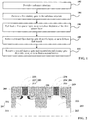
- FIG. 1 is a simplified flowchart of a method for manufacturing a semiconductor device. As shown in FIG. 1 , in step 102, a substrate structure is provided.
- FIG. 2 shows a schematic sectional diagram of one implementation of a substrate structure.
- the substrate structure includes: a substrate having a first device region 201 and a second device region 202, a first dummy gate structure 203 at the first device region 201, a second dummy gate structure 204 at the second device region 202 and a Lightly Doped Drain (LDD) region 205 in the substrate below the first dummy gate structure 203.
- the LDD region 205 facilitates to reduce Hot Carrier Effect (Hot Carrier Effect, HCE).
- HCE Hot Carrier Effect
- the substrate below the second dummy gate structure 204 may also be provided with an LDD region.
- the first device region 201 may include an input/output (I/O) device region
- the second device region for example, may include a core device region.
- the first device region 201 and the second device region 202 may be separated by using an isolation region 206, such as a shallow trench isolation (STI) region.
- the substrate structure may further include a raised first source/drain region 207 at two sides of the first dummy gate structure 203 and a second source/drain region 208 at two sides of the second dummy gate structure 204.
- an interlayer dielectric (ILD) layer 209 may be provided above the isolation region 206.
- ILD interlayer dielectric
- the first dummy gate structure 203 includes a first dummy gate dielectric layer 213 (such as an oxide of silicon) at the first device region 201, a first dummy gate 223 (such as polysilicon) on the first dummy gate dielectric layer 213, and a first spacer layer 233 (such as a nitride of silicon) at a side wall of the first dummy gate 223.
- a first dummy gate dielectric layer 213 such as an oxide of silicon
- a first dummy gate 223 such as polysilicon
- a first spacer layer 233 such as a nitride of silicon
- the second dummy gate structure 204 includes a second dummy gate dielectric layer 214 (such as an oxide of silicon) at the second device region 202, a second dummy gate 224 (such as polysilicon) on the second dummy gate dielectric layer 214, and a second spacer layer 234 (such as a nitride of silicon) at a side wall of the second dummy gate 224.
- a second dummy gate dielectric layer 214 such as an oxide of silicon
- second dummy gate 224 such as polysilicon
- a second spacer layer 234 such as a nitride of silicon
- the first device region 201 may include a first semiconductor region 211 and a first semiconductor fin 221 at the first semiconductor region 211
- the second device region 202 may include a second semiconductor region 212 and a second semiconductor fin 222 at the second semiconductor region 212.
- the first dummy gate structure 203 may span over the first semiconductor fin 221 and the second dummy gate structure 204 may span over the second semiconductor fin 222.
- the term “span” is understood as the following: for example, the first dummy gate structure spans over the first semiconductor fin refers to that an upper surface and a side wall of a portion above the first semiconductor fin are both formed with the first dummy gate structure, and the first dummy gate structure is further formed at a part of the surface of the first semiconductor region.
- the first dummy gate 223 is removed.
- the first dummy gate 223 may be removed using dry etching to expose the first spacer layer 233, as shown in FIG. 3 .
- step 106 the first spacer layer 233 is etched back to reduce a thickness of the first spacer layer 233, as shown in FIG. 4 .
- the exposed first dummy gate dielectric layer 213 is removed to form a first trench 501, as shown in FIG. 5 .
- a part of the first dummy gate dielectric layer 213 which is located below the first spacer layer 233 may also be removed.
- a width of the first spacer layer 233 width along a direction of a channel
- a width of the first dummy gate dielectric layer 213 (width along a direction of a channel) below the first spacer layer 233 may be about 30 angstroms.
- step 110 the second dummy gate 224 and the exposed second dummy gate dielectric layer 214 are removed to form a second trench 601, as shown in FIG. 6 . Similar to the above, in some implementations, when removing the exposed second dummy gate dielectric layer 214, a part of the second dummy gate dielectric layer 214 which is located below the second spacer layer 234 may also be removed.
- One method for manufacturing a semiconductor device is described above.
- a first dummy gate is removed, then a thickness of a first spacer layer is reduced by etching it back, and then a second dummy gate and an exposed second dummy gate dielectric layer are removed.
- the method of this implementation in a case in which thermal budget is not added, may increase an overlapping area of a channel region and an LDD region of a first device after a gate electrode is subsequently formed, so as to improve reliability of the device.
- the present invention provides a semiconductor device.
- the semiconductor device may include: a substrate having a first device region 201 and a second device region 202; a first trench 501 at the first device region 201; a first spacer layer 233 at a side wall of the first trench 501; an LDD region 205 below the first trench; a second trench 601 at the second device region 202; and a second spacer layer 234 at a side wall of the second trench 601.
- a thickness of the first spacer layer 233 is smaller than a thickness of the second spacer layer 234.
- the first device region 201 may be an I/O device region, and the second device region 202 may be a core device region.
- the first device region 201 may include a first semiconductor region 211 and a first semiconductor fin 221 at the first semiconductor region 211; and the second device region 202 may include a second semiconductor region 212 and a second semiconductor fin 222 at the second semiconductor region 212.
- the foregoing manufacturing method may further include the following steps:
- the gate dielectric layer 701 may include a high K dielectric layer with high K dielectric materials such as hafnium oxide, tantalum oxide, aluminum oxide, zirconium oxide, or titanium oxide.
- an interface layer such as a thermal oxide layer
- IL Interface Layer, IL
- a thermal oxide layer at the bottom portion of the first trench 501 and/or the bottom portion of the second trench 601 may further be formed to improve interface properties between the gate dielectric layer 701 and the bottom surfaces of the first trench 501 and/or the second trench 502, thereby improving reliability of the gate dielectric layer 701.
- a gate oxide layer may further be formed at the bottom portion of the first trench 501, where the gate oxide layer and the gate dielectric layer 701 which is subsequently deposited together are used as a gate dielectric layer of a first device (for example, an I/O device).
- a first device for example, an I/O device.
- the in-situ steam generation (in-situ steam generation, ISSG) process may be used to form the gate oxide layer at the bottom portion of the first trench 501.
- a gate material 801 for example, tungsten or other metallic materials, may be deposited on the gate dielectric layer 701, as shown in FIG. 8 .
- a TiN cap layer may be first deposited on the gate dielectric layer 701, and then the gate material 801 is deposited on the TiN cap layer.
- the first gate structure includes a first gate dielectric layer 701A at a bottom portion and a side wall of the first trench 501, and a first gate electrode 801A on the first gate dielectric layer 701A.
- the second gate structure includes a second gate dielectric layer 701B at a bottom portion and a side wall of the second trench 502, and a second gate electrode 801B on the second gate dielectric layer 701B.
- the present invention further provides another semiconductor device, with reference to FIG. 9 .
- the semiconductor device shown in FIG. 9 may further include a first gate structure and a second gate structure. Reference may be made to the foregoing description for specific structures of the first gate structure and the second gate structure, and details are not described herein again.
- the first dummy gate structure may span over the first semiconductor fin 221, and the second dummy gate structure may span over the second semiconductor fin 222.
- the first gate structure may further include a gate oxide layer between the bottom portion of the first trench 501 and the first gate dielectric layer 701A.
- the semiconductor device may further include an interface layer between the bottom portion of the first trench 501 and the first gate dielectric layer 701A, and between the bottom portion of the second trench 601 and the second gate dielectric layer 701B.
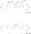
- FIG. 10A to FIG. 10J show schematic sectional drawings of various phases for forming a substrate structure shown in FIG. 2 . Detailed description is made in the following with reference to FIG. 10A to FIG. 10J .
- an initial substrate is provided.
- the initial substrate is etched to form the first device region and the second device region.
- a patterned hard mask 1002 may be formed on an initial substrate 1001.
- the initial substrate 1001 may be, for example, a semiconductor made of silicon (Si), germanium (Ge), or other elements, or may also be a semiconductor made of chemical compounds such as gallium arsenide (GaAs).
- a hard mask 1002 may be, for example, a nitride of silicon, an oxide of silicon, or a nitrogen oxide of silicon.
- the present invention is not limited thereto.
- the initial substrate 1001 is etched using the hard mask as a mask to form a substrate having a first device region 201 and a second device region 202.
- the first device region 201 includes a first semiconductor region 211 and a first semiconductor fin 221 at the first semiconductor region 211.
- the second device region 202 includes a second semiconductor region 212 and a second semiconductor fin 222 at the second semiconductor region 212.
- an isolation region is formed between various semiconductor fins, where a top surface of the isolation region is lower than a top surface of each semiconductor fin.
- an isolation material 1003 (for example, a dielectric material) may be deposited to fill up space between the various semiconductor fins and to cover the hard mask 1002.
- the isolation material 1003 may be deposited using, for example, technologies such as chemical vapor deposition (CVD) of flowable chemical vapour deposition (Flowable Chemical Vapour Deposition, FCVD).
- CVD chemical vapor deposition
- FCVD flowable Chemical Vapour Deposition
- a liner layer may further be formed at a surface of the substrate (that is, the first device region 201 and the second device region 202) (for example, forming a silicon oxide layer through thermal oxidation, not shown in the figures).
- the liner layer may repair surface damages caused to the first semiconductor fin 221 and the second semiconductor fin 222 when etching the initial substrate 1001.
- planarization for example, chemical-mechanical polishing, may further be performed to the isolation material 1003.
- the isolation material 1003 is etched back so that a height of the remaining isolation material 1003 reaches to an expected height, and the hard mask 1002 is exposed.
- the remaining isolation material 1003 after the etching back is an isolation region 206.
- a top surface of the isolation region 206 is lower than top surfaces of the first semiconductor fin 221 and the second semiconductor fin 222.
- the hard mask 1002 is removed.
- the hard mask 1002 may be removed using dry etching.
- ion implantation adjustment may be performed through threshold voltage (Vt).
- Vt threshold voltage
- a sacrificial oxide layer may be formed at surfaces of portions of the various semiconductor fins that are located above the isolation region, then the ion implantation adjustment is performed through threshold voltage, and then the sacrificial oxide layer is removed.
- dummy gate dielectric layers are formed at surfaces of portions of the various semiconductor fins that are located above the isolation region.
- a dummy gate dielectric layer 1004 such as a silicon oxide layer, is formed at surfaces of portions of the first semiconductor fin 221 and the second semiconductor fin 222 that are located above the isolation region 206.
- a dummy gate material is deposited, and the dummy gate material is patterned, so as to form a first dummy gate and a second dummy gate.
- the dummy gate material such as polysilicon
- the dummy gate material is deposited.
- the dummy gate material is patterned.
- a patterned hard mask is formed on the dummy gate material.
- the dummy gate material is etched using the hard mask as a mask and the dummy gate dielectric layer as a etch stop layer to form a first dummy gate 223 and a second dummy gate 224.
- a first spacer layer 233 such as a nitride of silicon
- a second spacer layer 234 such as a nitride of silicon
- silicon nitride layers may be deposited at the structure shown in FIG. 10G , and then the deposited silicon nitride layers are etched.
- a silicon nitride layer at a side wall of the first dummy gate 223 remains as the first spacer layer 233, and a silicon nitride layer at a side wall of the second dummy gate 224 remains as the second spacer layer 234.
- LDD injection is performed using the first spacer layer 233 as a mask, so as to form an LDD region 205, as shown in FIG. 10I .
- a portion of the first semiconductor fin 221 that is not covered by the first dummy gate structure 203 (including the dummy gate dielectric layer 1004 at a surface of the first semiconductor fin 221) is etched to form a recess.
- a semiconductor material is epitaxially grown in the recess, thereby forming a raised first source/drain region 207.
- a part of the second semiconductor fin 222 that is not covered by the second gate structure 204 (including the dummy gate dielectric layer 1004 at a surface of the second semiconductor fin 222) is etched to form a recess. Then, a semiconductor material is epitaxially grown in the recess, thereby forming a raised second source/drain region 208.
- the remaining dummy gate dielectric layer which is on the first semiconductor fin 221 is used as the first dummy gate dielectric layer 213, and remaining dummy gate dielectric layer which is on the second semiconductor fin 222 is used as the second dummy gate dielectric layer 214.
- an interlayer dielectric layer 209 for example, boron phosphate silicate glass, is deposited on the structure shown in FIG. 10I (also called as a first structure). Then, the interlayer dielectric layer 209 is planarized, to expose the first dummy gate 223 and the second dummy gate 224, as shown in FIG. 10J .
- a contact etch stop layer CESL (not shown in the figures) may be deposited on the first structure shown in FIG. 10I , and then, the interlayer dielectric layer 209 is deposited on the CESL to apply expected stress to a device.
- step 102 to step 110 may be executed according to the manner given above.
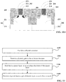
- FIG. 11 is a simplified flowchart of a method for manufacturing a semiconductor device according to another embodiment of the present invention. As shown in FIG. 11 , the method includes the following steps:
- a thickness of the spacer layer is reduced by etching it back after the dummy gate is removed, so that in a case in which thermal budget is not added, an overlapping area of a channel region and an LDD region of a device after a gate electrode is subsequently formed may be increased, so as to improve reliability of the device.
- a gate structure may be formed in the formed channel.
Landscapes
- Insulated Gate Type Field-Effect Transistor (AREA)
Abstract
Description
- The present application claims priority to Chinese Patent Appln. No.
201611046396.9, filed November 23, 2016 - The present invention relates to a technical field of semiconductors, and more particularly to a semiconductor device and a manufacturing method therefor.
- With a critical dimension of a metal oxide semiconductor field effect transistor (Metal Oxide Semiconductor Field Effect Transistor, MOSFET) decreasing, Short Channel Effect (Short Channel Effect, SCE) becomes a critical factor that affects device performances. A Fin Field Effect Transistor (Fin Field Effect Transistor, FinFET) has a better gate control ability, and can effectively suppress the short channel effect. Therefore, often a FinFET device is used in designing a semiconductor element of a smaller dimension.
- Regarding a System-On-a-Chip (System-On-a-Chip, SOC), different types of devices may need to be manufactured at the same time. For example, an input/output (I/O) device and a core device may need to be manufactured at the same time. To control a short channel effect of a core device, a smaller thermal budget is required. However, a smaller thermal budget results in an overlapping area of a Lightly Doped Drain (LDD) region and a channel region of the I/O device being smaller, thereby reducing a reliability of the I/O device. Other devices that are manufactured at the same time may experience the same problems.
- An object of the present invention is improving device reliability.
- The object is achieved by the features of the respective independent claims. Further embodiments and developments are defined in the dependent claims.
- In a first aspect of the present invention, a method for manufacturing a semiconductor device is provided. The method for manufacturing a semiconductor device comprises: providing a substrate structure, wherein the substrate structure comprises: a substrate, a first dummy gate structure on the substrate; and a Lightly Doped Drain, LDD, region below the first dummy gate structure, wherein the first dummy gate structure comprises a first dummy gate dielectric layer on the substrate, a first dummy gate on the first dummy gate dielectric layer, and a first spacer layer at a side wall of the first dummy gate; removing the first dummy gate; etching back the first spacer layer to reduce the thickness of the first spacer layer; and removing an exposed portion of the first dummy gate dielectric layer to from a trench.
- In a further development, wherein the substrate structure further comprises: a first device region and a second device region, the first dummy gate structure at the first device region, and a second dummy gate structure at the second device region, the second dummy gate structure comprises: a second dummy gate dielectric layer at the second device region, a second dummy gate on the second dummy gate dielectric layer, and a second spacer layer at a side wall of the second dummy gate; and the method further comprises: removing the second dummy gate and an exposed portion of the second dummy gate dielectric layer to form a second trench. Preferably, the method further includes: depositing a gate dielectric layer to cover a bottom portion and a side wall of the first trench and a bottom portion and a side wall of the second trench; and depositing a gate material on the gate dielectric layer.
- Preferably, the method further includes: before depositing a gate dielectric layer, forming an interface layer at the bottom portion of the first trench and the bottom portion of the second trench.
- Preferably, the method further includes: before depositing a gate dielectric layer, forming a gate oxide layer at the bottom portion of the first trench.
- Preferably, the first device region includes an I/O device region, and the second device region includes a core device region.
- Preferably, the first device region includes a first semiconductor region and a first semiconductor fin at the first semiconductor region; and the second device region includes a second semiconductor region and a second semiconductor fin at the second semiconductor region, where the first dummy gate structure spans over the first semiconductor fin and the second dummy gate structure spans over the second semiconductor fin.
- Preferably, providing a substrate structure may include: providing an initial the substrate; etching the initial substrate to form the first device region and the second device region; forming an isolation region between various semiconductor fins, where a top surface of the isolation region is lower than a top surface of each semiconductor fin; forming dummy gate dielectric layers at surfaces of portions of the various semiconductor fins that are located above the isolation region; depositing a dummy gate material and patterning the dummy gate material to form the first dummy gate and the second dummy gate; forming the first spacer layer at side walls of the first dummy gate and the first dummy gate dielectric layer, and forming the second spacer layer at side walls of the second dummy gate and the second dummy gate dielectric layer; performing LDD injection using the first spacer layer as a mask to form the LDD region to form a first structure; depositing an inter layer dielectric layer on the first structure; and planarizing the interlayer dielectric layer to expose the first dummy gate and the second dummy gate.
- Preferably, depositing an interlayer dielectric layer on the first structure may include: depositing a contact etch stop layer on the first structure; and depositing the interlayer dielectric layer on the contact etch stop layer.
- In a second aspect of the present invention, a semiconductor device is provided, including: a substrate having a first device region and a second device region; a first trench at the first device region; a first spacer layer at a side wall of the first trench; an LDD region below the first trench; a second trench at the second device region; and a second spacer layer at a side wall of the second trench, where a thickness of the first spacer layer is smaller than a thickness of the second spacer layer.
- Preferably, the device further includes a first gate structure and a second gate structure, where the first gate structure includes a first gate dielectric layer at a bottom portion and a side wall of the first trench, and a first gate electrode on the first gate dielectric layer; and the second gate structure includes a second gate dielectric layer at a bottom portion and a side wall of the second trench, and a second gate electrode on the second gate dielectric layer.
- Preferably, the first device region includes a first semiconductor region and a first semiconductor fin at the first semiconductor region; and the second device region includes a second semiconductor region and a second semiconductor fin at the second semiconductor region, where the first gate structure spans over the first semiconductor fin, and the second gate structure spans over the second semiconductor fin.
- Preferably, the device further includes: an interface layer between the bottom portion of the first trench and the first gate dielectric layer, and between the bottom portion of the second trench and the second gate dielectric layer.
- Preferably, the first gate structure further includes a gate oxide layer between the bottom portion of the first trench and the first gate dielectric layer.
- Preferably, the first device region includes an I/O device region, and the second device region includes a core device region.
- A device according to the second aspect of the present invention may be obtained by a method according to the first aspect of the present invention.
- In implementations of methods for manufacturing a semiconductor device provided by the present invention, a first dummy gate is first removed. Then a thickness of a first spacer layer is reduced by etching it back, and then, a second dummy gate and exposed second dummy gate dielectric layer are removed. Compared with simultaneously removing the first dummy gate and the second dummy gate as in the prior art, implementations of methods of the present invention, in a case in which thermal budget is not added, may increase an overlapping area of a channel region and an LDD region of a first device after a gate electrode is subsequently formed, so as to improve reliability of the device.
- In light of the following detailed descriptions of embodiments and implementations of the present invention for illustration purposes with reference to the accompanying drawings, other characters, aspects, and advantages of the present invention become clear.
- The accompanying drawings form a part of the specification, assist in describing embodiments and implementations of the present invention for illustration purposes, and are used to explain the principles of the present invention together with the specification. In the accompanying drawings:
-
FIG. 1 is a simplified flowchart of a method for manufacturing a semiconductor device; -
FIG. 2 to FIG. 6 show schematic sectional diagrams of various phases of a method for manufacturing a semiconductor device; -
FIG. 7 to FIG. 9 show schematic sectional diagrams of various phases of another method for manufacturing a semiconductor device; -
FIG. 10A to FIG. 10J show schematic sectional diagrams of various phases for forming a substrate structure shown inFIG. 2 ; and -
FIG. 11 is a simplified flowchart of a method for manufacturing a semiconductor device. - Embodiments and implementations of the present invention are described in detail for illustration purposes with reference to the accompanying drawings. It should be noted that unless being described in detail, relative layouts, mathematical expressions, and numeric values of components and steps described in these embodiments and implementations should not be understood as a limitation to the scope of the present invention.
- In addition, it should be understood that for ease of description, sizes of the parts shown in the accompanying drawings are not necessarily drawn according to an actual proportional relationship. For example, thicknesses or widths of some layers may be magnified with respect to other layers.
- The following description about the embodiments and implementations of the present invention are presented for illustration purposes only, and should not be used as a limitation on the present invention and applications or uses of the present invention in any sense.
- Technologies, methods, and devices that are known by a person of ordinary skill in the related fields may not be discussed in detail. However, in cases in which the technologies, methods, and devices are applicable, the technologies, methods, and devices should be considered as a part of the description.
- It should be noted that similar reference signs and letters are used to represent similar items in the following accompanying drawings. Therefore, once an item is defined or described in a figure, the item needs not to be further discussed in the description of the subsequent figures.
- Regarding the foregoing problem, the inventor has found that to increase an overlapping area of an LDD region and a channel region, dose of injecting the LDD may be increased. However, after the dose of injecting the LDD is increased, a reliability of some devices such as an I/O device may decrease. On this basis, the inventor provides the following solutions to address this problem.
-
FIG. 1 is a simplified flowchart of a method for manufacturing a semiconductor device. As shown inFIG. 1 , instep 102, a substrate structure is provided. -
FIG. 2 shows a schematic sectional diagram of one implementation of a substrate structure. As shown inFIG. 2 , the substrate structure includes: a substrate having afirst device region 201 and asecond device region 202, a firstdummy gate structure 203 at thefirst device region 201, a seconddummy gate structure 204 at thesecond device region 202 and a Lightly Doped Drain (LDD)region 205 in the substrate below the firstdummy gate structure 203. TheLDD region 205 facilitates to reduce Hot Carrier Effect (Hot Carrier Effect, HCE). It should be understood that the substrate below the seconddummy gate structure 204 may also be provided with an LDD region. In some implementations, thefirst device region 201, for example, may include an input/output (I/O) device region, and the second device region, for example, may include a core device region. Thefirst device region 201 and thesecond device region 202 may be separated by using anisolation region 206, such as a shallow trench isolation (STI) region. In addition, the substrate structure may further include a raised first source/drain region 207 at two sides of the firstdummy gate structure 203 and a second source/drain region 208 at two sides of the seconddummy gate structure 204. In addition, an interlayer dielectric (ILD)layer 209 may be provided above theisolation region 206. - As shown in
FIG. 2 , the firstdummy gate structure 203 includes a first dummy gate dielectric layer 213 (such as an oxide of silicon) at thefirst device region 201, a first dummy gate 223 (such as polysilicon) on the first dummygate dielectric layer 213, and a first spacer layer 233 (such as a nitride of silicon) at a side wall of thefirst dummy gate 223. The seconddummy gate structure 204 includes a second dummy gate dielectric layer 214 (such as an oxide of silicon) at thesecond device region 202, a second dummy gate 224 (such as polysilicon) on the second dummygate dielectric layer 214, and a second spacer layer 234 (such as a nitride of silicon) at a side wall of thesecond dummy gate 224. It should be understood that thefirst spacer layer 233 may also be on the first dummygate dielectric layer 213, and thesecond spacer layer 234 may also be on the second dummygate dielectric layer 214. - In some implementations, as shown in
FIG. 2 , thefirst device region 201 may include afirst semiconductor region 211 and afirst semiconductor fin 221 at thefirst semiconductor region 211, and thesecond device region 202 may include asecond semiconductor region 212 and asecond semiconductor fin 222 at thesecond semiconductor region 212. In such a case, the firstdummy gate structure 203 may span over thefirst semiconductor fin 221 and the seconddummy gate structure 204 may span over thesecond semiconductor fin 222. It should be noted that in the present context, the term "span" is understood as the following: for example, the first dummy gate structure spans over the first semiconductor fin refers to that an upper surface and a side wall of a portion above the first semiconductor fin are both formed with the first dummy gate structure, and the first dummy gate structure is further formed at a part of the surface of the first semiconductor region. - Subsequently, in
step 104, thefirst dummy gate 223 is removed. For example, thefirst dummy gate 223 may be removed using dry etching to expose thefirst spacer layer 233, as shown inFIG. 3 . - Subsequently, in
step 106, thefirst spacer layer 233 is etched back to reduce a thickness of thefirst spacer layer 233, as shown inFIG. 4 . - Subsequently, in
step 108, the exposed first dummygate dielectric layer 213 is removed to form afirst trench 501, as shown inFIG. 5 . It should be understood that when removing the exposed first dummygate dielectric layer 213, a part of the first dummygate dielectric layer 213 which is located below thefirst spacer layer 233 may also be removed. For example, a width of the first spacer layer 233 (width along a direction of a channel) may be about 50-80 angstroms, and a width of the first dummy gate dielectric layer 213 (width along a direction of a channel) below thefirst spacer layer 233 may be about 30 angstroms. - Subsequently, in
step 110, thesecond dummy gate 224 and the exposed second dummygate dielectric layer 214 are removed to form asecond trench 601, as shown inFIG. 6 . Similar to the above, in some implementations, when removing the exposed second dummygate dielectric layer 214, a part of the second dummygate dielectric layer 214 which is located below thesecond spacer layer 234 may also be removed. - One method for manufacturing a semiconductor device is described above. In the described method, a first dummy gate is removed, then a thickness of a first spacer layer is reduced by etching it back, and then a second dummy gate and an exposed second dummy gate dielectric layer are removed. Compared with simultaneously removing the first dummy gate and the second dummy gate in the prior art, the method of this implementation, in a case in which thermal budget is not added, may increase an overlapping area of a channel region and an LDD region of a first device after a gate electrode is subsequently formed, so as to improve reliability of the device.
- Corresponding to the foregoing method, the present invention provides a semiconductor device. With reference to
FIG. 6 , the semiconductor device may include: a substrate having afirst device region 201 and asecond device region 202; afirst trench 501 at thefirst device region 201; afirst spacer layer 233 at a side wall of thefirst trench 501; anLDD region 205 below the first trench; asecond trench 601 at thesecond device region 202; and asecond spacer layer 234 at a side wall of thesecond trench 601. Herein, a thickness of thefirst spacer layer 233 is smaller than a thickness of thesecond spacer layer 234. - For example, the
first device region 201 may be an I/O device region, and thesecond device region 202 may be a core device region. In one implementation, with reference toFIG. 6 , thefirst device region 201 may include afirst semiconductor region 211 and afirst semiconductor fin 221 at thefirst semiconductor region 211; and thesecond device region 202 may include asecond semiconductor region 212 and asecond semiconductor fin 222 at thesecond semiconductor region 212. - In some embodiments, after the
first trench 501 and thesecond trench 601 shown inFIG. 6 are formed, the foregoing manufacturing method may further include the following steps: - Depositing a
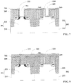
gate dielectric layer 701 to cover a bottom portion and a side wall of thefirst trench 501 and a bottom portion and a side wall of thesecond trench 601, as shown inFIG. 7 . Preferably, thegate dielectric layer 701 may include a high K dielectric layer with high K dielectric materials such as hafnium oxide, tantalum oxide, aluminum oxide, zirconium oxide, or titanium oxide. Preferably, before depositing thegate dielectric layer 701, an interface layer (Interface Layer, IL), such as a thermal oxide layer, at the bottom portion of thefirst trench 501 and/or the bottom portion of thesecond trench 601 may further be formed to improve interface properties between thegate dielectric layer 701 and the bottom surfaces of thefirst trench 501 and/or the second trench 502, thereby improving reliability of thegate dielectric layer 701. - Some devices, such as an I/O device, may need a gate dielectric layer thicker than a core device. Therefore, in some implementations, preferably, before depositing the
gate dielectric layer 701, a gate oxide layer may further be formed at the bottom portion of thefirst trench 501, where the gate oxide layer and thegate dielectric layer 701 which is subsequently deposited together are used as a gate dielectric layer of a first device (for example, an I/O device). For example, the in-situ steam generation (in-situ steam generation, ISSG) process may be used to form the gate oxide layer at the bottom portion of thefirst trench 501. - Subsequently, a
gate material 801, for example, tungsten or other metallic materials, may be deposited on thegate dielectric layer 701, as shown inFIG. 8 . In some implementations, a TiN cap layer may be first deposited on thegate dielectric layer 701, and then thegate material 801 is deposited on the TiN cap layer. - Subsequently, a planarization process such as chemical-mechanical polishing (CMP) may be performed until an
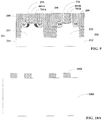
interlayer dielectric layer 209 is exposed to form a first gate structure and a second gate structure, as shown inFIG. 9 . Herein, the first gate structure includes a firstgate dielectric layer 701A at a bottom portion and a side wall of thefirst trench 501, and a first gate electrode 801A on the firstgate dielectric layer 701A. The second gate structure includes a secondgate dielectric layer 701B at a bottom portion and a side wall of the second trench 502, and asecond gate electrode 801B on the secondgate dielectric layer 701B. - Correspondingly, the present invention further provides another semiconductor device, with reference to
FIG. 9 . Compared with the semiconductor device shown inFIG. 6 , the semiconductor device shown inFIG. 9 may further include a first gate structure and a second gate structure. Reference may be made to the foregoing description for specific structures of the first gate structure and the second gate structure, and details are not described herein again. - In addition, as shown in
FIG. 9 , in a case in which thefirst device region 201 includes afirst semiconductor fin 221 and thesecond device region 202 includes asecond semiconductor fin 222, the first dummy gate structure may span over thefirst semiconductor fin 221, and the second dummy gate structure may span over thesecond semiconductor fin 222. In addition, in some implementations, the first gate structure may further include a gate oxide layer between the bottom portion of thefirst trench 501 and the firstgate dielectric layer 701A. - In some implementations, the semiconductor device may further include an interface layer between the bottom portion of the
first trench 501 and the firstgate dielectric layer 701A, and between the bottom portion of thesecond trench 601 and the secondgate dielectric layer 701B. -
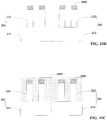
FIG. 10A to FIG. 10J show schematic sectional drawings of various phases for forming a substrate structure shown inFIG. 2 . Detailed description is made in the following with reference toFIG. 10A to FIG. 10J . - First, an initial substrate is provided. The initial substrate is etched to form the first device region and the second device region.
- For example, as shown in
FIG. 10A , a patternedhard mask 1002 may be formed on aninitial substrate 1001. Theinitial substrate 1001 may be, for example, a semiconductor made of silicon (Si), germanium (Ge), or other elements, or may also be a semiconductor made of chemical compounds such as gallium arsenide (GaAs). Ahard mask 1002 may be, for example, a nitride of silicon, an oxide of silicon, or a nitrogen oxide of silicon. However, the present invention is not limited thereto. - Following this, as shown in
FIG. 10B , theinitial substrate 1001 is etched using the hard mask as a mask to form a substrate having afirst device region 201 and asecond device region 202. Thefirst device region 201 includes afirst semiconductor region 211 and afirst semiconductor fin 221 at thefirst semiconductor region 211. Thesecond device region 202 includes asecond semiconductor region 212 and asecond semiconductor fin 222 at thesecond semiconductor region 212. - Subsequently, an isolation region is formed between various semiconductor fins, where a top surface of the isolation region is lower than a top surface of each semiconductor fin.
- For example, as shown in
FIG. 10C , an isolation material 1003 (for example, a dielectric material) may be deposited to fill up space between the various semiconductor fins and to cover thehard mask 1002. For example, theisolation material 1003 may be deposited using, for example, technologies such as chemical vapor deposition (CVD) of flowable chemical vapour deposition (Flowable Chemical Vapour Deposition, FCVD). Optionally, before theisolation material 1003 is deposited, a liner layer may further be formed at a surface of the substrate (that is, thefirst device region 201 and the second device region 202) (for example, forming a silicon oxide layer through thermal oxidation, not shown in the figures). The liner layer may repair surface damages caused to thefirst semiconductor fin 221 and thesecond semiconductor fin 222 when etching theinitial substrate 1001. After theisolation material 1003 is deposited, planarization, for example, chemical-mechanical polishing, may further be performed to theisolation material 1003. - Following this, for example, as shown in
FIG. 10D , theisolation material 1003 is etched back so that a height of the remainingisolation material 1003 reaches to an expected height, and thehard mask 1002 is exposed. Herein, the remainingisolation material 1003 after the etching back is anisolation region 206. A top surface of theisolation region 206 is lower than top surfaces of thefirst semiconductor fin 221 and thesecond semiconductor fin 222. Subsequently, for example, as shown inFIG. 10E , thehard mask 1002 is removed. For example, thehard mask 1002 may be removed using dry etching. - Optionally, ion implantation adjustment may be performed through threshold voltage (Vt). For example, a sacrificial oxide layer may be formed at surfaces of portions of the various semiconductor fins that are located above the isolation region, then the ion implantation adjustment is performed through threshold voltage, and then the sacrificial oxide layer is removed.
- Subsequently, dummy gate dielectric layers are formed at surfaces of portions of the various semiconductor fins that are located above the isolation region.
- As shown in
FIG. 10F , a dummygate dielectric layer 1004, such as a silicon oxide layer, is formed at surfaces of portions of thefirst semiconductor fin 221 and thesecond semiconductor fin 222 that are located above theisolation region 206. - Subsequently, a dummy gate material is deposited, and the dummy gate material is patterned, so as to form a first dummy gate and a second dummy gate.
- As shown in
FIG. 10G , the dummy gate material, such as polysilicon, is deposited. Then, the dummy gate material is patterned. For example, a patterned hard mask is formed on the dummy gate material. Following this, the dummy gate material is etched using the hard mask as a mask and the dummy gate dielectric layer as a etch stop layer to form afirst dummy gate 223 and asecond dummy gate 224. - Subsequently, a
first spacer layer 233, such as a nitride of silicon, is formed at a side wall of thefirst dummy gate 223. Moreover, asecond spacer layer 234, such as a nitride of silicon, is formed at a side wall of thesecond dummy gate 224, as shown inFIG. 10H . For example, silicon nitride layers may be deposited at the structure shown inFIG. 10G , and then the deposited silicon nitride layers are etched. A silicon nitride layer at a side wall of thefirst dummy gate 223 remains as thefirst spacer layer 233, and a silicon nitride layer at a side wall of thesecond dummy gate 224 remains as thesecond spacer layer 234. - Subsequently, LDD injection is performed using the
first spacer layer 233 as a mask, so as to form anLDD region 205, as shown inFIG. 10I . Subsequently, a portion of thefirst semiconductor fin 221 that is not covered by the first dummy gate structure 203 (including the dummygate dielectric layer 1004 at a surface of the first semiconductor fin 221) is etched to form a recess. Then, a semiconductor material is epitaxially grown in the recess, thereby forming a raised first source/drain region 207. - Similarly, a part of the
second semiconductor fin 222 that is not covered by the second gate structure 204 (including the dummygate dielectric layer 1004 at a surface of the second semiconductor fin 222) is etched to form a recess. Then, a semiconductor material is epitaxially grown in the recess, thereby forming a raised second source/drain region 208. The remaining dummy gate dielectric layer which is on thefirst semiconductor fin 221 is used as the first dummygate dielectric layer 213, and remaining dummy gate dielectric layer which is on thesecond semiconductor fin 222 is used as the second dummygate dielectric layer 214. - Subsequently, an
interlayer dielectric layer 209, for example, boron phosphate silicate glass, is deposited on the structure shown inFIG. 10I (also called as a first structure). Then, theinterlayer dielectric layer 209 is planarized, to expose thefirst dummy gate 223 and thesecond dummy gate 224, as shown inFIG. 10J . In other implementations, first, a contact etch stop layer (CESL) (not shown in the figures) may be deposited on the first structure shown inFIG. 10I , and then, theinterlayer dielectric layer 209 is deposited on the CESL to apply expected stress to a device. - As mentioned above, the substrate structure shown in
FIG. 2 is formed.Subsequent step 102 to step 110 may be executed according to the manner given above. -
FIG. 11 is a simplified flowchart of a method for manufacturing a semiconductor device according to another embodiment of the present invention. As shown inFIG. 11 , the method includes the following steps: -
Step 1102, provide a substrate structure. The substrate structure includes: a substrate, for example, a semiconductor substrate made of silicon; a dummy gate structure on the substrate; and a Lightly Doped Drain (LDD) region below the dummy gate structure. The dummy gate structure includes a dummy gate dielectric layer (such as an oxide of silicon) on the substrate, a dummy gate (such as polysilicon) on the dummy gate dielectric layer, and a spacer layer (such as a nitride of silicon) at a side wall of the dummy gate. In some implementations, the substrate may include a semiconductor region and a semiconductor fin at the semiconductor region, and the dummy gate structure spans over the semiconductor fin. -
Step 1104, remove the dummy gate, so as to expose the spacer layer. -
Step 1106, etch back the spacer layer, so as to reduce a thickness of the spacer layer. -
Step 1108, remove exposed dummy gate dielectric layer, so as to form a trench. It should be understood that when removing the exposed dummy gate dielectric layer, a part of the dummy gate dielectric layer which is located below the spacer layer may also be removed. - In this implementation, a thickness of the spacer layer is reduced by etching it back after the dummy gate is removed, so that in a case in which thermal budget is not added, an overlapping area of a channel region and an LDD region of a device after a gate electrode is subsequently formed may be increased, so as to improve reliability of the device.
- In some implementations, a gate structure may be formed in the formed channel.
- Above, a semiconductor device and a manufacturing method therefor according to the implementations of the present invention are described in detail. In describing the present invention, some details generally known in the art are not described. According to the foregoing description, a person skilled in the art may completely understand how to implement the technical solutions disclosed herein. In addition, the embodiments and implementations according to the teaching disclosed in the specification may be freely combined. A person skilled in the art should understand that various amendments may be made to the embodiments and implementations described above without departing from the spirit and scope of the present invention that are defined by the appended claims.
Claims (15)
- A method for manufacturing a semiconductor device, comprising:providing a substrate structure, wherein the substrate structure comprises:a substrate,a first dummy gate structure on the substrate; anda Lightly Doped Drain, LDD, region below the first dummy gate structure,wherein the first dummy gate structure comprises a first dummy gate dielectric layer on the substrate, a first dummy gate on the first dummy gate dielectric layer, and a first spacer layer at a side wall of the first dummy gate;removing the first dummy gate;etching back the first spacer layer to reduce the thickness of the first spacer layer; andremoving an exposed portion of the first dummy gate dielectric layer to from a trench.
- The method according to claim 1, wherein
the substrate structure further comprises:a first device region and a second device region,the first dummy gate structure at the first device region, anda second dummy gate structure at the second device region,the second dummy gate structure comprises:a second dummy gate dielectric layer at the second device region,a second dummy gate on the second dummy gate dielectric layer, anda second spacer layer at a side wall of the second dummy gate; and the method further comprises:removing the second dummy gate and an exposed portion of the second dummy gate dielectric layer to form a second trench. - The method according to claim 2, further comprising:depositing a gate dielectric layer to cover a bottom portion and a side wall of the first trench and a bottom portion and a side wall of the second trench; anddepositing a gate material on the gate dielectric layer.
- The method according to claim 3, further comprising:before depositing the gate dielectric layer, forming an interface layer at the bottom portion of the first trench and the bottom portion of the second trench.
- The method according to any one of the claims 3 or 4, further comprising:before depositing the gate dielectric layer, forming a gate oxide layer at the bottom portion of the first trench.
- The method according to any one of the claims 2-5, wherein the first device region comprises an input/output (I/O) device region, and the second device region comprises a core device region.
- The method according to any one of the claims 2-6, wherein
the first device region comprises a first semiconductor region and a first semiconductor fin at the first semiconductor region; and
the second device region comprises a second semiconductor region and a second semiconductor fin at the second semiconductor region,
wherein the first dummy gate structure spans over the first semiconductor fin and the second dummy gate structure spans over the second semiconductor fin. - The method according to claim 7, wherein steps of providing the substrate structure comprises:providing an initial substrate;etching the initial substrate to form the first device region and the second device region;forming an isolation region between one or more semiconductor fins, wherein a top surface of the isolation region is lower than a top surface of each semiconductor fin;forming dummy gate dielectric layers at surfaces of portions of the one or more semiconductor fins that are located above the isolation region;depositing a dummy gate material and patterning the dummy gate material to form the first dummy gate and the second dummy gate;forming the first spacer layer at a side wall of the first dummy gate, and forming the second spacer layer at a side wall of the second dummy gate;performing LDD injection by using the first spacer layer as a mask to form the LDD region, so as to form a first structure;depositing an interlayer dielectric layer on the first structure; andplanarizing the interlayer dielectric layer to expose the first dummy gate and the second dummy gate.
- The method according to claim 8, wherein depositing the interlayer dielectric layer on the first structure comprises:depositing a contact etch stop layer on the first structure; anddepositing the interlayer dielectric layer on the contact etch stop layer.
- A semiconductor device, comprising:a substrate having a first device region and a second device region;a first trench at the first device region;a first spacer layer at a side wall of the first trench;a Lightly Doped Drain, LDD, region below the first trench;a second trench at the second device region; anda second spacer layer at a side wall of the second trench,wherein a thickness of the first spacer layer is smaller than a thickness of the second spacer layer.
- The device according to claim 10, further comprising:a first gate structure, wherein the first gate structure comprises a first gate dielectric layer at a bottom portion and a side wall of the first trench, and a first gate electrode on the first gate dielectric layer; anda second gate structure, wherein the second gate structure comprises a second gate dielectric layer at a bottom portion and a side wall of the second trench, and a second gate electrode on the second gate dielectric layer.
- The device according to claim 11, wherein
the first device region comprises a first semiconductor region and a first semiconductor fin at the first semiconductor region; and
the second device region comprises a second semiconductor region and a second semiconductor fin at the second semiconductor region,
wherein the first gate structure spans over the first semiconductor fin, and the second gate structure spans over the second semiconductor fin. - The device according to claim 11 or 12, further comprising:an interface layer between the bottom portion of the first trench and the first gate dielectric layer, and between the bottom portion of the second trench and the second gate dielectric layer.
- The device according to any one of the claims 11-13, wherein
the first gate structure further comprises a gate oxide layer between the bottom portion of the first trench and the first gate dielectric layer. - The device according to any one of the claims 10-14, wherein the first device region comprises an I/O device region, and the second device region comprises a core device region.
Applications Claiming Priority (1)
| Application Number | Priority Date | Filing Date | Title |
|---|---|---|---|
| CN201611046396.9A CN108091651B (en) | 2016-11-23 | 2016-11-23 | Semiconductor device and method of manufacturing the same |
Publications (1)
| Publication Number | Publication Date |
|---|---|
| EP3327765A1 true EP3327765A1 (en) | 2018-05-30 |
Family
ID=60450433
Family Applications (1)
| Application Number | Title | Priority Date | Filing Date |
|---|---|---|---|
| EP17202699.9A Withdrawn EP3327765A1 (en) | 2016-11-23 | 2017-11-21 | Semiconductor device and manufacturing method therefor |
Country Status (3)
| Country | Link |
|---|---|
| US (2) | US10461188B2 (en) |
| EP (1) | EP3327765A1 (en) |
| CN (1) | CN108091651B (en) |
Families Citing this family (6)
| Publication number | Priority date | Publication date | Assignee | Title |
|---|---|---|---|---|
| CN107799421B (en) * | 2016-09-05 | 2021-04-02 | 中芯国际集成电路制造(上海)有限公司 | Method of forming a semiconductor device |
| CN109830433B (en) * | 2017-11-23 | 2021-03-30 | 联华电子股份有限公司 | Method of making semiconductor element |
| US10903336B2 (en) * | 2017-11-28 | 2021-01-26 | Taiwan Semiconductor Manufacturing Co., Ltd. | Semiconductor device and method of manufacturing the same |
| CN113972273B (en) * | 2020-07-24 | 2025-01-17 | 中芯国际集成电路制造(上海)有限公司 | Semiconductor structure and forming method thereof |
| CN114497214B (en) * | 2020-10-23 | 2025-06-27 | 中芯国际集成电路制造(上海)有限公司 | Semiconductor structure and method for forming the same |
| US20240105722A1 (en) * | 2022-09-23 | 2024-03-28 | Taiwan Semiconductor Manufacturing Company, Ltd. | Semiconductor device |
Citations (7)
| Publication number | Priority date | Publication date | Assignee | Title |
|---|---|---|---|---|
| EP0932197A1 (en) * | 1998-01-27 | 1999-07-28 | Lsi Logic Corporation | Method of varying MOS transistor electrical characteristics of integrated circuits |
| US20070287259A1 (en) * | 2006-06-08 | 2007-12-13 | Kavalieros Jack T | Forming ultra-shallow junctions |
| US20140179076A1 (en) * | 2012-12-25 | 2014-06-26 | Renesas Electronics Corporation | Manufacturing method of semiconductor device |
| US20150041925A1 (en) * | 2012-11-30 | 2015-02-12 | Institute of Microelectronics, Chinese Academy of Sciences | P type mosfet and method for manufacturing the same |
| US20150069516A1 (en) * | 2013-09-10 | 2015-03-12 | Texas Instruments Incorporated | Inner l-spacer for replacement gate flow |
| US9105742B1 (en) * | 2014-03-27 | 2015-08-11 | International Business Machines Corporation | Dual epitaxial process including spacer adjustment |
| US20160079124A1 (en) * | 2014-09-11 | 2016-03-17 | Institute of Microelectroics, Chinese Academy of Sciences | Method for manufacturing semiconductor device |
Family Cites Families (17)
| Publication number | Priority date | Publication date | Assignee | Title |
|---|---|---|---|---|
| JP2005101196A (en) * | 2003-09-24 | 2005-04-14 | Hitachi Ltd | Manufacturing method of semiconductor integrated circuit device |
| JP5076388B2 (en) * | 2006-07-28 | 2012-11-21 | 富士通セミコンダクター株式会社 | Semiconductor device and manufacturing method thereof |
| US20080237734A1 (en) * | 2007-03-29 | 2008-10-02 | United Microelectronics Corp. | Complementary metal-oxide-semiconductor transistor and method of fabricating the same |
| KR101964262B1 (en) * | 2011-11-25 | 2019-04-02 | 삼성전자주식회사 | Semiconductor device and method of manufacturing same |
| JP5816560B2 (en) * | 2012-01-10 | 2015-11-18 | ルネサスエレクトロニクス株式会社 | Semiconductor device and manufacturing method thereof |
| US20150213564A1 (en) | 2012-08-27 | 2015-07-30 | Hitachi, Ltd. | Consumer cooperation support apparatus |
| CN103839816B (en) * | 2012-11-25 | 2019-04-19 | 中国科学院微电子研究所 | Semiconductor device and method of manufacturing the same |
| US9362386B2 (en) * | 2013-02-27 | 2016-06-07 | Taiwan Semiconductor Manufacturing Company, Ltd. | FETs and methods for forming the same |
| US9269714B2 (en) * | 2013-06-10 | 2016-02-23 | Globalfoundries Inc. | Device including a transistor having a stressed channel region and method for the formation thereof |
| CN104867873B (en) * | 2014-02-21 | 2018-03-20 | 中芯国际集成电路制造(上海)有限公司 | A kind of manufacture method of semiconductor devices |
| US9064890B1 (en) * | 2014-03-24 | 2015-06-23 | Globalfoundries Inc. | Methods of forming isolation material on FinFET semiconductor devices and the resulting devices |
| US9337316B2 (en) * | 2014-05-05 | 2016-05-10 | Taiwan Semiconductor Manufacturing Company, Ltd. | Method for FinFET device |
| US9190272B1 (en) * | 2014-07-15 | 2015-11-17 | Samsung Electronics Co., Ltd. | Semiconductor device and method of fabricating the same |
| CN105489652B (en) * | 2014-09-19 | 2018-09-18 | 中国科学院微电子研究所 | Semiconductor device and manufacturing method thereof |
| US9515188B2 (en) * | 2014-12-22 | 2016-12-06 | Taiwan Semiconductor Manufacturing Company, Ltd. | Fin field effect transistors having conformal oxide layers and methods of forming same |
| US9711533B2 (en) * | 2015-10-16 | 2017-07-18 | Taiwan Semiconductor Manufacturing Company, Ltd. | FinFET devices having different source/drain proximities for input/output devices and non-input/output devices and the method of fabrication thereof |
| US10276565B2 (en) * | 2017-03-23 | 2019-04-30 | Taiwan Semiconductor Manufacturing Co., Ltd. | Semiconductor device and manufacturing method thereof |
-
2016
- 2016-11-23 CN CN201611046396.9A patent/CN108091651B/en active Active
-
2017
- 2017-11-15 US US15/814,154 patent/US10461188B2/en active Active
- 2017-11-21 EP EP17202699.9A patent/EP3327765A1/en not_active Withdrawn
-
2019
- 2019-09-20 US US16/577,732 patent/US10964813B2/en active Active
Patent Citations (7)
| Publication number | Priority date | Publication date | Assignee | Title |
|---|---|---|---|---|
| EP0932197A1 (en) * | 1998-01-27 | 1999-07-28 | Lsi Logic Corporation | Method of varying MOS transistor electrical characteristics of integrated circuits |
| US20070287259A1 (en) * | 2006-06-08 | 2007-12-13 | Kavalieros Jack T | Forming ultra-shallow junctions |
| US20150041925A1 (en) * | 2012-11-30 | 2015-02-12 | Institute of Microelectronics, Chinese Academy of Sciences | P type mosfet and method for manufacturing the same |
| US20140179076A1 (en) * | 2012-12-25 | 2014-06-26 | Renesas Electronics Corporation | Manufacturing method of semiconductor device |
| US20150069516A1 (en) * | 2013-09-10 | 2015-03-12 | Texas Instruments Incorporated | Inner l-spacer for replacement gate flow |
| US9105742B1 (en) * | 2014-03-27 | 2015-08-11 | International Business Machines Corporation | Dual epitaxial process including spacer adjustment |
| US20160079124A1 (en) * | 2014-09-11 | 2016-03-17 | Institute of Microelectroics, Chinese Academy of Sciences | Method for manufacturing semiconductor device |
Also Published As
| Publication number | Publication date |
|---|---|
| US20200020806A1 (en) | 2020-01-16 |
| US20180145172A1 (en) | 2018-05-24 |
| US10964813B2 (en) | 2021-03-30 |
| CN108091651B (en) | 2021-03-30 |
| US10461188B2 (en) | 2019-10-29 |
| CN108091651A (en) | 2018-05-29 |
Similar Documents
| Publication | Publication Date | Title |
|---|---|---|
| US10964813B2 (en) | Semiconductor device and manufacturing method therefor | |
| US9685531B2 (en) | Method for manufacturing semiconductor device having metal gate | |
| US10418456B2 (en) | Method of fabricating a semiconductor device having modified profile metal gate | |
| TWI651761B (en) | Semiconductor devices and methods for forming the same | |
| KR101910243B1 (en) | A semiconductor device and a method for fabricating the same | |
| US20210273106A1 (en) | Flat sti surface for gate oxide uniformity in fin fet devices | |
| US20130161762A1 (en) | Gate structure for semiconductor device | |
| TW202002280A (en) | Semiconductor devices and methods for forming the same | |
| CN110660859A (en) | Manufacturing method of semiconductor device | |
| US10483263B2 (en) | Semiconductor device and manufacturing method therefor | |
| CN103489784B (en) | There is semiconductor device and the manufacture method thereof of the gate height uniformity of improvement | |
| TW201731104A (en) | Gate structure, semiconductor device, and method of forming the same | |
| US10236216B2 (en) | Method for manufacturing a semiconductor device having a fin located on a substrate | |
| TW201923899A (en) | Method of fabricating semiconductor device | |
| CN102237399B (en) | Semiconductor element with metal gate and manufacturing method thereof | |
| TW201421693A (en) | FinFET component and its forming method | |
| TWI775731B (en) | Fin field effect transistor and method for fabricating the same | |
| US20160133744A1 (en) | Transistor and fabrication method thereof | |
| KR20130043046A (en) | Semiconductor device having metal gate electrode and method of fabrication thereof | |
| CN107516649A (en) | Semiconductor device and manufacturing method thereof | |
| CN110491837A (en) | Internal L spacers for replacement gate flow | |
| CN102299092B (en) | Semiconductor device and forming method thereof | |
| US10686081B2 (en) | Semiconductor device, MOS capacitor, and manufacturing methods therefor | |
| CN104253079A (en) | Shallow trench isolation structure, transistor including same and manufacturing method thereof | |
| CN107452793A (en) | Semiconductor device and its manufacture method |
Legal Events
| Date | Code | Title | Description |
|---|---|---|---|
| PUAI | Public reference made under article 153(3) epc to a published international application that has entered the european phase |
Free format text: ORIGINAL CODE: 0009012 |
|
| STAA | Information on the status of an ep patent application or granted ep patent |
Free format text: STATUS: THE APPLICATION HAS BEEN PUBLISHED |
|
| AK | Designated contracting states |
Kind code of ref document: A1 Designated state(s): AL AT BE BG CH CY CZ DE DK EE ES FI FR GB GR HR HU IE IS IT LI LT LU LV MC MK MT NL NO PL PT RO RS SE SI SK SM TR |
|
| AX | Request for extension of the european patent |
Extension state: BA ME |
|
| STAA | Information on the status of an ep patent application or granted ep patent |
Free format text: STATUS: REQUEST FOR EXAMINATION WAS MADE |
|
| 17P | Request for examination filed |
Effective date: 20180810 |
|
| RBV | Designated contracting states (corrected) |
Designated state(s): AL AT BE BG CH CY CZ DE DK EE ES FI FR GB GR HR HU IE IS IT LI LT LU LV MC MK MT NL NO PL PT RO RS SE SI SK SM TR |
|
| RAP1 | Party data changed (applicant data changed or rights of an application transferred) |
Owner name: SEMICONDUCTOR MANUFACTURING INTERNATIONAL (BEIJING Owner name: SEMICONDUCTOR MANUFACTURING INTERNATIONAL (SHANGHA |
|
| STAA | Information on the status of an ep patent application or granted ep patent |
Free format text: STATUS: EXAMINATION IS IN PROGRESS |
|
| 17Q | First examination report despatched |
Effective date: 20201126 |
|
| STAA | Information on the status of an ep patent application or granted ep patent |
Free format text: STATUS: THE APPLICATION IS DEEMED TO BE WITHDRAWN |
|
| 18D | Application deemed to be withdrawn |
Effective date: 20210407 |