EP3327754A1 - A semiconductor device and manufacture thereof - Google Patents
A semiconductor device and manufacture thereof Download PDFInfo
- Publication number
- EP3327754A1 EP3327754A1 EP17203753.3A EP17203753A EP3327754A1 EP 3327754 A1 EP3327754 A1 EP 3327754A1 EP 17203753 A EP17203753 A EP 17203753A EP 3327754 A1 EP3327754 A1 EP 3327754A1
- Authority
- EP
- European Patent Office
- Prior art keywords
- layer
- source region
- insulation layer
- cavity
- dielectric layer
- Prior art date
- Legal status (The legal status is an assumption and is not a legal conclusion. Google has not performed a legal analysis and makes no representation as to the accuracy of the status listed.)
- Withdrawn
Links
Images






Classifications
-
- H—ELECTRICITY
- H10—SEMICONDUCTOR DEVICES; ELECTRIC SOLID-STATE DEVICES NOT OTHERWISE PROVIDED FOR
- H10D—INORGANIC ELECTRIC SEMICONDUCTOR DEVICES
- H10D64/00—Electrodes of devices having potential barriers
- H10D64/01—Manufacture or treatment
- H10D64/017—Manufacture or treatment using dummy gates in processes wherein at least parts of the final gates are self-aligned to the dummy gates, i.e. replacement gate processes
-
- H—ELECTRICITY
- H10—SEMICONDUCTOR DEVICES; ELECTRIC SOLID-STATE DEVICES NOT OTHERWISE PROVIDED FOR
- H10D—INORGANIC ELECTRIC SEMICONDUCTOR DEVICES
- H10D30/00—Field-effect transistors [FET]
- H10D30/60—Insulated-gate field-effect transistors [IGFET]
-
- H—ELECTRICITY
- H10—SEMICONDUCTOR DEVICES; ELECTRIC SOLID-STATE DEVICES NOT OTHERWISE PROVIDED FOR
- H10D—INORGANIC ELECTRIC SEMICONDUCTOR DEVICES
- H10D30/00—Field-effect transistors [FET]
- H10D30/01—Manufacture or treatment
- H10D30/021—Manufacture or treatment of FETs having insulated gates [IGFET]
-
- H—ELECTRICITY
- H10—SEMICONDUCTOR DEVICES; ELECTRIC SOLID-STATE DEVICES NOT OTHERWISE PROVIDED FOR
- H10D—INORGANIC ELECTRIC SEMICONDUCTOR DEVICES
- H10D62/00—Semiconductor bodies, or regions thereof, of devices having potential barriers
- H10D62/10—Shapes, relative sizes or dispositions of the regions of the semiconductor bodies; Shapes of the semiconductor bodies
- H10D62/17—Semiconductor regions connected to electrodes not carrying current to be rectified, amplified or switched, e.g. channel regions
- H10D62/213—Channel regions of field-effect devices
- H10D62/221—Channel regions of field-effect devices of FETs
- H10D62/235—Channel regions of field-effect devices of FETs of IGFETs
-
- H—ELECTRICITY
- H10—SEMICONDUCTOR DEVICES; ELECTRIC SOLID-STATE DEVICES NOT OTHERWISE PROVIDED FOR
- H10D—INORGANIC ELECTRIC SEMICONDUCTOR DEVICES
- H10D62/00—Semiconductor bodies, or regions thereof, of devices having potential barriers
- H10D62/80—Semiconductor bodies, or regions thereof, of devices having potential barriers characterised by the materials
- H10D62/82—Heterojunctions
- H10D62/822—Heterojunctions comprising only Group IV materials heterojunctions, e.g. Si/Ge heterojunctions
-
- H—ELECTRICITY
- H10—SEMICONDUCTOR DEVICES; ELECTRIC SOLID-STATE DEVICES NOT OTHERWISE PROVIDED FOR
- H10D—INORGANIC ELECTRIC SEMICONDUCTOR DEVICES
- H10D64/00—Electrodes of devices having potential barriers
- H10D64/01—Manufacture or treatment
- H10D64/013—Manufacture or treatment of electrodes having a conductor capacitively coupled to a semiconductor by an insulator
- H10D64/01302—Manufacture or treatment of electrodes having a conductor capacitively coupled to a semiconductor by an insulator the insulator being formed after the semiconductor body, the semiconductor being silicon
- H10D64/01332—Making the insulator
-
- H—ELECTRICITY
- H10—SEMICONDUCTOR DEVICES; ELECTRIC SOLID-STATE DEVICES NOT OTHERWISE PROVIDED FOR
- H10D—INORGANIC ELECTRIC SEMICONDUCTOR DEVICES
- H10D64/00—Electrodes of devices having potential barriers
- H10D64/60—Electrodes characterised by their materials
- H10D64/66—Electrodes having a conductor capacitively coupled to a semiconductor by an insulator, e.g. MIS electrodes
-
- H—ELECTRICITY
- H10—SEMICONDUCTOR DEVICES; ELECTRIC SOLID-STATE DEVICES NOT OTHERWISE PROVIDED FOR
- H10D—INORGANIC ELECTRIC SEMICONDUCTOR DEVICES
- H10D84/00—Integrated devices formed in or on semiconductor substrates that comprise only semiconducting layers, e.g. on Si wafers or on GaAs-on-Si wafers
- H10D84/01—Manufacture or treatment
- H10D84/0123—Integrating together multiple components covered by H10D12/00 or H10D30/00, e.g. integrating multiple IGBTs
- H10D84/0126—Integrating together multiple components covered by H10D12/00 or H10D30/00, e.g. integrating multiple IGBTs the components including insulated gates, e.g. IGFETs
- H10D84/013—Manufacturing their source or drain regions, e.g. silicided source or drain regions
-
- H—ELECTRICITY
- H10—SEMICONDUCTOR DEVICES; ELECTRIC SOLID-STATE DEVICES NOT OTHERWISE PROVIDED FOR
- H10D—INORGANIC ELECTRIC SEMICONDUCTOR DEVICES
- H10D84/00—Integrated devices formed in or on semiconductor substrates that comprise only semiconducting layers, e.g. on Si wafers or on GaAs-on-Si wafers
- H10D84/01—Manufacture or treatment
- H10D84/02—Manufacture or treatment characterised by using material-based technologies
- H10D84/03—Manufacture or treatment characterised by using material-based technologies using Group IV technology, e.g. silicon technology or silicon-carbide [SiC] technology
- H10D84/038—Manufacture or treatment characterised by using material-based technologies using Group IV technology, e.g. silicon technology or silicon-carbide [SiC] technology using silicon technology, e.g. SiGe
-
- H—ELECTRICITY
- H10—SEMICONDUCTOR DEVICES; ELECTRIC SOLID-STATE DEVICES NOT OTHERWISE PROVIDED FOR
- H10P—GENERIC PROCESSES OR APPARATUS FOR THE MANUFACTURE OR TREATMENT OF DEVICES COVERED BY CLASS H10
- H10P14/00—Formation of materials, e.g. in the shape of layers or pillars
- H10P14/40—Formation of materials, e.g. in the shape of layers or pillars of conductive or resistive materials
-
- H—ELECTRICITY
- H10—SEMICONDUCTOR DEVICES; ELECTRIC SOLID-STATE DEVICES NOT OTHERWISE PROVIDED FOR
- H10P—GENERIC PROCESSES OR APPARATUS FOR THE MANUFACTURE OR TREATMENT OF DEVICES COVERED BY CLASS H10
- H10P30/00—Ion implantation into wafers, substrates or parts of devices
- H10P30/20—Ion implantation into wafers, substrates or parts of devices into semiconductor materials, e.g. for doping
- H10P30/22—Ion implantation into wafers, substrates or parts of devices into semiconductor materials, e.g. for doping using masks
-
- H—ELECTRICITY
- H10—SEMICONDUCTOR DEVICES; ELECTRIC SOLID-STATE DEVICES NOT OTHERWISE PROVIDED FOR
- H10P—GENERIC PROCESSES OR APPARATUS FOR THE MANUFACTURE OR TREATMENT OF DEVICES COVERED BY CLASS H10
- H10P52/00—Grinding, lapping or polishing of wafers, substrates or parts of devices
- H10P52/40—Chemomechanical polishing [CMP]
- H10P52/403—Chemomechanical polishing [CMP] of conductive or resistive materials
-
- H—ELECTRICITY
- H10—SEMICONDUCTOR DEVICES; ELECTRIC SOLID-STATE DEVICES NOT OTHERWISE PROVIDED FOR
- H10W—GENERIC PACKAGES, INTERCONNECTIONS, CONNECTORS OR OTHER CONSTRUCTIONAL DETAILS OF DEVICES COVERED BY CLASS H10
- H10W20/00—Interconnections in chips, wafers or substrates
- H10W20/01—Manufacture or treatment
- H10W20/071—Manufacture or treatment of dielectric parts thereof
Definitions
- This present invention relates to semiconductor technology and, more specifically, to a semiconductor device and its manufacturing method.
- MOSFET Metal Oxide Semiconductor Field Effect Transistor
- a semiconductor fin 101, a Shallow Trench Isolation (STI) 102, and a well region are first formed, then a pseudo gate structure is formed.
- the pseudo gate structure comprises a pseudo gate insulation layer 103, a pseudo gate electrode 104, and a hard mask layer 105.
- the pseudo gate electrode 104 has a height of H 1 , as shown in Fig. 1A .
- a spacer 106 is formed, and a source electrode 107 and a drain electrode 108 are epitaxially grown. Then an ion implantation process is conducted in the source electrode 107 and the drain electrode 108, a silicon nitride layer 109 covering the whole structure is formed, and an Interlayer Dielectric (ILD) layer 110 is deposited on the silicon nitride layer 109.
- ILD Interlayer Dielectric
- a planarization process is conducted on the structure of Fig. 1B to expose the pseudo gate electrode 104.
- the pseudo gate electrode 104 and the pseudo gate insulation layer 103 are both removed to form a gate structure, which comprises a gate oxide layer 111, a high-K (K is the dielectric constant) dielectric layer 112 and a metal gate electrode 113.
- the process to form the gate structure comprises: forming the gate oxide layer 111 through an oxidation process; depositing the high-K dielectric layer 112 and a gate material layer 113; and conducting a Chemical Mechanical Planarization (CMP) process to form the gate structure.
- the gate material layer may comprise a work function regulation layer and a metal layer on the work function regulation layer.
- the process to form the gate structure may further comprise a process to pre-clean the surface of the semiconductor fin 101 and a process to form an interlayer (IL) layer.
- the metal gate electrode 113 has a height of H 2 , as shown in Fig. 1D .
- metal contact components (not shown in the figures) connecting the metal gate electrode, the source electrode, and the drain electrode are formed.
- the metal gate electrode has a height loss of H 1 - H 2 , the height loss is largely due to the CMP process, the etching process, and the wet cleaning process that may be conducted in the planarization process to expose the pseudo gate electrode, the process to remove the pseudo gate electrode, the pre-clean process, and the CMP process on the gate structure.
- a structure with too large H 1 may block the ion implantation process or cause the pseudo gate electrode to peel off; while a structure with too small H 2 may have a homogeneous issue as a result of drifts or variations in the heights of different devices.
- H 2 is too small, metal contact components may only contact the metal gate electrodes in some devices, but not in other devices.
- a small H 1 and a large H 2 are preferred in a gate manufacturing process.
- the inventors of this present invention investigate the large loss of the interlayer dielectric layer in conventional manufacturing methods, which leads to a large height loss of the gate electrode.
- This present invention provides both a semiconductor device and its manufacturing method.
- the present invention disclosed herein can reduce the loss of the interlayer dielectric layer in the manufacturing process and therefore reduce the height loss of the gate electrode.
- a first of the present invention provides a semiconductor device manufacturing method, comprising: providing a semiconductor structure, wherein the semiconductor structure comprises: a substrate; at least one source region on the substrate; an interlayer dielectric layer covering a portion of the source region, wherein the interlayer dielectric layer has a cavity on the source region; and a pseudo gate insulation layer at the bottom of the cavity covering a portion of the source region; forming a barrier layer in the cavity; forming a loss reduction region in the interlayer dielectric layer by conducting an ion implantation process comprising silicon ion or carbon ion on the semiconductor structure; removing the barrier layer; removing the pseudo gate insulation layer to expose a portion of the source region; and forming a gate structure on the exposed portion of the source region.
- the ion used in the ion implantation process may comprise silicon ion, carbon ion, or an ionic group comprising silicon or carbon.
- providing a semiconductor structure may comprise: providing an initial structure, wherein the initial structure comprises: a substrate; at least one source region on the substrate; a pseudo gate structure on the source region, wherein the pseudo gate structure comprises a pseudo gate insulation layer on the source region and a pseudo gate electrode on the pseudo gate insulation layer; and an interlayer dielectric layer around the pseudo gate structure, wherein the upper surface of the interlayer dielectric layer is on substantially the same horizontal level as the upper surface of the pseudo gate electrode; and removing the pseudo gate electrode to form a cavity.
- the interlayer dielectric layer may comprise a first insulation layer on the source region and a second insulation layer on the first insulation layer
- providing a semiconductor structure may comprise: providing an initial structure, wherein the initial structure comprises: a substrate; at least one source region on the substrate; a pseudo gate structure on the source region, wherein the pseudo gate structure comprises a pseudo gate insulation layer on the source region and a pseudo gate electrode on the pseudo gate insulation layer; and the first insulation layer around the pseudo gate structure, wherein the upper surface of the first insulation layer is on substantially the same horizontal level as the upper surface of the pseudo gate electrode; removing the pseudo gate electrode to form a cavity; and forming the second insulation layer on the first insulation layer and on the bottom and a sidewall of the cavity, wherein the barrier layer is formed on the second insulation layer.
- the method may further comprise removing the second insulation layer in the cavity after the barrier layer is removed but before the pseudo gate insulation layer is removed.
- the method may further comprise conducting a thermal annealing process on the semiconductor structure with the loss reduction region after the barrier layer is removed but before the second insulation layer in the cavity is removed.
- the gate structure may comprise: a gate insulation layer on the exposed portion of the source region; a high-K dielectric layer on the gate insulation layer; and a gate electrode on the high-K dielectric layer.
- forming a gate structure on the exposed portion of the source region may comprise: forming a gate insulation layer on the exposed portion of the source region; forming a high-K dielectric layer on the gate insulation layer covering the semiconductor structure; forming a gate material layer on the high-K dielectric layer; and forming the gate structure by conducting a planarization process on the semiconductor structure after the gate material layer is formed.
- the barrier layer may comprise a Bottom Anti-Reflective Coating (BARC) layer or a photoresist.
- BARC Bottom Anti-Reflective Coating
- forming a barrier layer in the cavity may comprise: forming a barrier layer filling the cavity on the semiconductor structure; and removing a portion of the barrier layer so that the remaining barrier layer partially fills the cavity.
- the source region may comprise a first source region for a first device and a second source region for a second device
- the interlayer dielectric layer may comprise a first part of the interlayer dielectric layer covering a portion of the first source region and a second part of the interlayer dielectric layer covering a portion of the second source region
- the cavity may comprise a first cavity on the first source region and a second cavity on the second source region.
- removing the pseudo gate insulation layer may comprise: forming a hard mask layer on the second part of the interlayer dielectric layer and in the second cavity; removing the pseudo gate insulation layer in the first cavity to expose a portion of the first source region; and removing the hard mask layer.
- the method may further comprise conducting a thermal annealing process on the semiconductor structure with the loss reduction region after the barrier layer is removed but before the hard mask layer is formed.
- removing the pseudo gate insulation layer may comprise: forming a cover layer on the second part of the interlayer dielectric layer and in the second cavity; forming a hard mask layer on the cover layer; removing the pseudo gate insulation layer in the first cavity to expose a portion of the first source region; and removing the hard mask layer and the cover layer.
- the method may further comprise conducting a thermal annealing process on the semiconductor structure with the loss reduction region after the barrier layer is removed but before the cover layer is formed.
- removing the barrier layer may comprise: removing the barrier layer in the first cavity, and wherein removing the pseudo gate insulation layer comprises: forming a hard mask layer on the second part of the interlayer dielectric layer and on the barrier layer in the second cavity; removing the pseudo gate insulation layer in the first cavity to expose a portion of the first source region; and removing the hard mask layer and the barrier layer in the second cavity.
- removing the barrier layer may comprise: removing the barrier layer in the first cavity, and removing the pseudo gate insulation layer comprises: forming a cover layer on the second part of the interlayer dielectric layer and on the barrier layer in the second cavity; forming a hard mask layer on the cover layer; removing the pseudo gate insulation layer in the first cavity to expose a portion of the first source region; and removing the hard mask layer, the cover layer and the barrier layer in the second cavity.
- forming a gate structure may comprise: forming a gate insulation layer on the expose portion of the first source region; forming a high-K dielectric layer in the first cavity and in the second cavity; and forming a gate electrode on the high-K dielectric layer.
- the semiconductor structure may further comprise: a source electrode and a drain electrode in the source region and each at a side of the cavity; and a spacer on a sidewall of the cavity.
- the aforementioned method may further comprise: forming a groove around the source region, and the semiconducting structure further comprises: a third insulation layer at least partially filling the groove; and a fourth insulation layer covering the third insulation layer, the source electrode, and the drain electrode, wherein the interlayer dielectric layer is formed on the fourth insulation layer.
- the source region may be a semiconductor fin or a source region for a planar semiconductor device.
- a second aspect of the present invention provides a semiconductor device, comprising: a substrate; at least one source region on the substrate; a gate structure on the source region; an interlayer dielectric layer around the gate structure, wherein the interlayer dielectric layer has a loss reduction region formed by conducting an ion implantation process comprising silicon ion or carbon ion on the interlayer dielectric layer.
- the gate structure may comprise: a gate insulation layer on the source region; a high-K dielectric layer on the gate insulation layer; and a gate electrode on the high-K dielectric layer.
- the upper surface of the interlayer dielectric layer may be on substantially the same horizontal level as the upper surface of the gate electrode.
- the interlayer dielectric layer may comprise: a first insulation layer covering a portion of the source region; and a second insulation layer on the first insulation layer.
- the source region may comprise: a first source region for a first device; and a second source region for a second device.
- the device may further comprise: a source electrode and a drain electrode in the source region and each at a side of the gate electrode; and a spacer on the source region and located between the gate electrode and the source electrode, and between the gate electrode and the drain electrode.
- the device may further comprise: a groove around the source region; a third insulation layer at least partially filling the groove; and a fourth insulation layer covering the third insulation layer, the source electrode, and the drain electrode, wherein the interlayer dielectric layer is formed on the fourth insulation layer.
- the source region may be a semiconductor fin or a source region for a planar semiconductor device.
- the device according to the second aspect of the present invention may be obtained by a method according to the first aspect of the present invention.
- Embodiments in the figures may represent idealized illustrations. Variations from the shapes illustrated may be possible, for example due to manufacturing techniques and/or tolerances. Thus, the example embodiments shall not be construed as limited to the shapes or regions illustrated herein but are to include deviations in the shapes. For example, an etched region illustrated as a rectangle may have rounded or curved features. The shapes and regions illustrated in the figures are illustrative and shall not limit the invention.
- first,” “second,” etc. may be used herein to describe various elements, these elements shall not be limited by these terms. These terms may be used to distinguish one element from another element. Thus, a first element discussed below may be termed a second element without departing from the teachings of the present present invention. The description of an element as a “first” element may not require or imply the presence of a second element or other elements.
- the terms “first,” “second,” etc. may also be used herein to differentiate different categories or sets of elements. For conciseness, the terms “first,” “second,” etc. may represent “first-category (or first-set),” “second-category (or second-set),” etc., respectively.
- first element such as a layer, film, region, or substrate
- neighbored to or “coupled with” a second element
- the first element can be directly on, directly neighboring, directly connected to or directly coupled with the second element, or an intervening element may also be present between the first element and the second element.
- first element is referred to as being “directly on,” “directly neighboring,” “directly connected to,” or “directly coupled with” a second element, then no intended intervening element (except environmental elements such as air) may also be present between the first element and the second element.
- spatially relative terms such as “beneath,” “below,” “lower,” “above,” “upper,” and the like, may be used herein for ease of description to describe one element or feature's spatial relationship to another element(s) or feature(s) as illustrated in the figures. It will be understood that the spatially relative terms may encompass different orientations of the device in use or operation in addition to the orientation depicted in the figures. For example, if the device in the figures is turned over, elements described as “below” or “beneath” other elements or features would then be oriented “above” the other elements or features. Thus, the term “below” can encompass both an orientation of above and below. The device may be otherwise oriented (rotated 90 degrees or at other orientation), and the spatially relative descriptors used herein shall be interpreted accordingly.
- connection may mean “electrically connect.”
- insulation may mean “electrically insulate.”
- Embodiments of the present invention may also cover an article of manufacture that includes a non-transitory computer readable medium on which computer-readable instructions for carrying out embodiments of the inventive technique are stored.
- the computer readable medium may include, for example, semiconductor, magnetic, opto-magnetic, optical, or other forms of computer readable medium for storing computer readable code.
- the present invention may also cover apparatuses for practicing embodiments of the present invention. Such apparatus may include circuits, dedicated and/or programmable, to carry out operations pertaining to embodiments of the present invention.
- Examples of such apparatus include a general purpose computer and/or a dedicated computing device when appropriately programmed and may include a combination of a computer/computing device and dedicated/programmable hardware circuits (such as electrical, mechanical, and/or optical circuits) adapted for the various operations pertaining to embodiments of the present invention.
- a general purpose computer and/or a dedicated computing device when appropriately programmed and may include a combination of a computer/computing device and dedicated/programmable hardware circuits (such as electrical, mechanical, and/or optical circuits) adapted for the various operations pertaining to embodiments of the present invention.
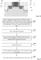
- Fig. 2 shows a flowchart illustrating a semiconductor device manufacturing method in accordance with one or more embodiments of this present invention.
- a semiconductor structure comprises a substrate, at least one source region on the substrate; an interlayer dielectric layer covering a portion of the source region, wherein the interlayer dielectric layer has a cavity on the source region; and a pseudo gate insulation layer on the bottom of the cavity covering a portion of the source region.
- a barrier layer is formed in the cavity.
- the barrier layer may comprise a Bottom Anti-Reflective Coating (BARC) layer or a photoresist.
- BARC Bottom Anti-Reflective Coating
- step S206 an ion implantation process comprising silicon ion or carbon ion is conducted on the semiconductor structure to form a loss reduction region in the interlayer dielectric layer.
- the ions that are implanted in the ion implantation process may comprise silicon ion, carbon ion, or an ionic group comprising silicon or carbon.
- step S208 the barrier layer is removed.
- step S210 the pseudo gate insulation layer is removed to expose a portion of the source region.
- a gate structure is formed on the exposed portion of the source region.
- the gate structure may comprise a gate insulation layer on the exposed portion of the source region, a high-K dielectric layer on the gate insulation layer, and a gate electrode on the high-K dielectric layer.
- the gate insulation layer may comprise silicon dioxide
- the high-K dielectric layer may comprise a silicon nitride, aluminum oxide (Al 2 O 3 ), yttrium oxide (Y 2 O 3 ), lanthanum oxide (La 2 O 3 ), tantalum pentoxide (Ta 2 O 5 ), titanium dioxide (TiO 2 ), hafnium dioxide (HfO 2 ), or zirconium dioxide (ZrO 2 ).
- the gate electrode may be made of a metallic material such as tungsten.
- the gate electrode may also comprise materials for work function regulation layer such as titanium nitride, tantalum nitride, or titanium aluminum alloy.
- a loss reduction region is formed in the interlayer dielectric layer by conducting an ion implantation process comprising silicon ion or carbon ion on the semiconductor structure, the loss reduction region can reduce the loss of interlayer dielectric layer, and reduce the height loss of the gate electrode, in the succeeding stages that involve an etching or a planarization process (for example, step S210 may involve an etching process and step S212 may involve a planarization process).
- this present invention allows a lower pseudo gate electrode and a higher gate electrode than those in conventional methods.
- the manufacturing method of this present invention provides more manufacture margin than conventional methods and helps to improve production yield.
- the source region may be either a semiconductor fin or a source region for a planar device. That it, this present invention can apply to either a fin-type semiconductor device or a planar semiconductor device. For conciseness, this present invention will be described using only examples where the source region is a semiconductor fin.
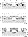
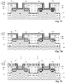
- FIGS. 3A, 3B, 3C , 3D, 3E, 3F , 3G, 3H, and 3I show schematic sectional views illustrating different stages of a semiconductor device manufacturing method in accordance with one or more embodiments of this present invention. This semiconductor device manufacturing method will be described in details with reference to these drawings.
- Figs. 3A and 3B show schematic sectional views illustrating two stages of this semiconducting manufacturing method corresponding to step S202.
- an initial structure is first provided.
- This initial structure may comprise a substrate 300 (e.g., a silicon substrate) and at least one source region 301 (e.g., a semiconductor fin) on the substrate 300.
- the initial structure may further comprise a pseudo gate structure on the source region 301.
- the pseudo gate structure may comprise a pseudo gate insulation layer 302 (e.g., a silicon dioxide layer) on the source region 301, and a pseudo gate electrode 305 (e.g., polycrystalline silicon) on the pseudo gate insulation layer 302.
- the initial structure may further comprise an interlayer dielectric layer 310 (e.g., a silicon dioxide layer) around the pseudo gate structure.
- the upper surface of the interlayer dielectric layer 310 is on substantially the same horizontal level as the upper surface of the pseudo gate electrode 305.
- substantially the same means that the horizontal difference between the upper surface of the interlayer dielectric layer 310 and the upper surface of the pseudo gate electrode 305 is within an acceptable range,
- the upper surface of the interlayer dielectric layer 310 and the upper surface of the pseudo gate electrode 305 may be made at "substantially the same” horizontal level by a same planarization process.
- This present invention is not limited herein though. Additionally, the dash lines in the drawings serve for an illustrative purpose to distinguish different regions only, and do not represent any structural components in the devices.
- the initial structure may further comprise a source electrode 307 and a drain electrode 308 in the source region 301 and each at a side of the pseudo gate structure.
- the initial structure may further comprise a spacer 306 on the source region 301 and located between the source electrode 307 and the pseudo gate electrode 305, and between the drain electrode 308 and the pseudo gate electrode 305.
- the spacer 306 may comprise silicon dioxide or silicon nitride.
- a groove may be formed around the source region 301, and, optionally, the initial structure may further comprise a third insulation layer 303 (e.g., a silicon dioxide layer) at least partially filling the groove, a fourth insulation layer 304 (e.g., a silicon nitride layer) covering the third insulation layer 303, the source electrode 307, and the drain electrode 308, wherein the interlayer dielectric layer 310 is formed on fourth insulation layer 304.
- a third insulation layer 303 e.g., a silicon dioxide layer
- fourth insulation layer 304 e.g., a silicon nitride layer
- the pseudo gate electrode 305 is removed to form a cavity 311, and a semiconductor structure corresponding to step S202 is formed.
- This semiconductor structure comprises a substrate 300 and at least one source region 301 on the substrate 300.
- This semiconductor structure may further comprise an interlayer dielectric layer 310 partially covering the source region 301, wherein the interlayer dielectric layer 310 has a cavity 311 on the source region 301.
- This semiconductor structure may further comprise a pseudo gate insulation layer 302 at the bottom of the cavity 311 covering a portion the source region 301.
- this semiconductor structure may further comprise a source electrode 307 and a drain electrode 308 in the source region 301 and each at a side of the cavity 311.
- This semiconductor structure may further comprise a spacer 306 on a sidewall of the cavity 311.
- a groove may be formed around the source region 301, and, optionally, this semiconductor structure may further comprise a third insulation layer 303 at least partially filling the groove, a fourth insulation layer 304 covering the third insulation layer 303, the source electrode 307, and the drain electrode 308, wherein the interlayer dielectric layer 310 is formed on the fourth insulation layer 304.
- the process to form the barrier layer comprises: forming a barrier layer 312 filling the cavity 311 on the semiconductor structure through deposition or coating.
- the process to form the barrier layer may further comprise removing a portion of the barrier layer 312 so that the remaining barrier layer 312 partially fills the cavity 311, and the upper surface of the interlayer dielectric layer 310 is exposed.
- a loss reduction region 313 is formed in the interlayer dielectric layer 310 by conducting an ion implantation process comprising silicon ion or carbon ion on the semiconductor structure.
- the ion used in the ion implantation process may comprise silicon ion, carbon ion, or an ionic group comprising silicon or carbon.
- the energy for the ion implantation process is in a range of 1 KeV to 10 KeV (e.g., 5 KeV).
- the implantation dose may be in a range of 1 ⁇ 10 12 atom/cm 2 to 1 ⁇ 10 16 atom/cm 2
- Silicon or carbon implanted into the interlayer dielectric layer 310 can reduce the loss of the interlayer dielectric layer 310 in succeeding etching or planarization processes, and thus reduces the height loss of the gate electrode. Additionally, the barrier layer 312 formed on the source region 301 can prevent silicon ion, carbon ion, or an ionic group comprising silicon or carbon from being implanted into the source region 301 in the ion implantation process.
- the ion implantation process may also implant the ions into the spacer 106 and/or the fourth insulation layer 304, thus form a loss reduction region in those regions as well.
- the spacer 106 and the fourth insulation layer 304 are thinner than the interlayer dielectric layer 310, the loss reduction region formed in these regions has a less loss reduction effect than that formed in the interlayer dielectric layer 310. Therefore, the loss reduction region in the spacer 106 and the fourth insulation layer 304 is not shown in the drawing.
- a loss reduction region may also be formed in the spacer 106 and/or the fourth insulation layer 304.
- the barrier layer 312 is removed.
- the barrier layer 312 may be removed by an etching process that has a high etch selectivity ratio to silicon oxide or silicon nitride, such as Reactive Ion Etching (RIE) or wet etching.
- RIE Reactive Ion Etching
- the pseudo gate insulation layer 302 is removed by an etching process to expose a portion of the source region 301.
- the process to form the gate structure may comprise: forming a gate insulation layer 321 (e.g., a silicon dioxide layer) on the exposed portion of the source region 301 through a deposition or an oxidation process; forming a high-K dielectric layer 322 on the gate insulation layer 321 covering the semiconductor structure; and forming a gate material layer 323 on the high-K dielectric layer 322.
- the process to form the gate structure may further comprise: forming a gate structure 320 by conducting a planarization process on the semiconductor structure after the gate material layer 323 is formed.
- a loss reduction region is formed in the interlayer dielectric layer by conducting an ion implantation process comprising silicon ion or carbon ion.
- the loss reduction region can reduce the loss of the interlayer dielectric layer in the succeeding etching or planarization processes, and thus reduce the height loss of the gate electrode.
- this present invention also presents a semiconductor device.
- this semiconductor device comprises a substrate 300 and at least one source region 301 on the substrate 300.
- This semiconductor device may further comprise a gate structure 320 on the source region 301, and an interlayer dielectric layer 310 around the gate structure 320.
- the interlayer dielectric layer 310 has a loss reduction region 313 that is formed by ion implanting silicon or carbon ions into the interlayer dielectric layer 310. That is, the loss reduction region 313 comprise silicon or carbon.
- the gate structure 320 comprises: a gate insulation layer 321 on the source region 301, a high-K dielectric layer 322 on the gate insulation layer 321, and a gate electrode 323 on the high-K dielectric layer 322.
- the upper surface of the interlayer dielectric layer 310 is on substantially the same horizontal level as the upper surface of the gate electrode 323.
- the semiconductor device may further comprise: a source electrode 307 and a drain electrode 308 in the source region 301 and each at a side of the gate electrode 323.
- the semiconductor device may further comprise a spacer 306 on the source region 301 and located between the gate electrode 323 and the source electrode 307, and between the gate electrode 323 and the drain electrode 308.
- a groove is formed around the source region 301.
- the semiconductor device may further comprise a third insulation layer 303 at least partially filling the groove.
- the semiconductor device may further comprise a fourth insulation layer 304 covering the third insulation layer 303, the source electrode 307, and the drain electrode 308, and the interlayer dielectric layer 310 is on the fourth dielectric layer 304.
- the source region 301 may be a semiconductor fin or a source region of a planar device.
- FIGS. 4A, 4B, 4C , 4D, 4E, 4F , 4G, and 4H show schematic sectional views illustrating different stages of a semiconductor device manufacturing method in accordance with one or more embodiments of this present invention. This semiconductor device manufacturing method will be described in details with reference to these drawings.
- an initial structure is first provided.
- This initial structure may comprise a substrate 400 and at least one source region 401 on the substrate 400.
- the initial structure may further comprise a pseudo gate structure on the source region 401.
- the pseudo gate structure may comprise a pseudo gate insulation layer 402 on the source region 401, and a pseudo gate electrode 405 on the pseudo gate insulation layer 402.
- the initial structure may further comprise a first insulation layer 4101 (e.g., a silicon dioxide layer) around the pseudo gate structure.
- the upper surface of the first insulation layer 4101 is on substantially the same horizontal level as the upper surface of the pseudo gate electrode 405.
- the initial structure may further comprise a source electrode 407, a drain electrode 408, a spacer 406, a third insulation layer 403, and a fourth insulation layer 404.
- These structures or components are the same as or similar to, respectively, the source electrode 307, the drain electrode 308, the spacer 306, the third insulation layer 303, and the fourth insulation layer 304 shown in Fig. 3A , thus are not repeatedly described here.
- the pseudo gate electrode 405 is removed to form a cavity 411.
- a second insulation layer 4102 is formed by a deposition method (e.g., Atomic Layer Deposition (ALD)) on the first insulation layer 4101 and on the bottom and the sidewall of the cavity 411.
- the second insulation layer 4102 may comprise silicon dioxide or silicon nitride.
- a portion of the first insulation layer 4101 and a portion of the second insulation layer 4102 may together form an interlayer dielectric layer 410. That is, the interlayer dielectric layer 410 comprises a portion of the first insulation layer 4101 covering the source region 401 and a portion of the second insulation layer 4102 on that portion of the first insulation layer 4101.
- FIG. 4C This concludes the description of the semiconductor structure shown in Fig. 4C .
- This semiconductor structure is similar to the semiconductor structure shown in Fig. 3B .
- the difference between these two semiconductor structures is that the interlayer dielectric layer shown in Fig. 3B has a single layer structure while the interlayer dielectric layer shown in Fig. 4C has a multi-layer structure (e.g., two-layer structure).
- a barrier layer 412 is formed in the cavity 411.
- the barrier layer 412 is formed on the second insulation layer 4102.
- a loss reduction region 413 is formed in the interlayer dielectric layer 410 by conducting an ion implantation process comprising silicon ion or carbon ion on the semiconductor structure.
- the loss reduction region 413 is formed in the second insulation layer 4102. In another embodiment, the loss reduction region 413 may also be formed in the first insulation layer 4101.
- the barrier layer 412 is removed. After the barrier layer 412 is removed, the second insulation layer 4102 in the cavity 411 is also removed.
- the manufacturing method may further comprise conducting a thermal annealing process on the semiconductor structure after the barrier layer 412 is removed but before the second insulation layer 4102 in the cavity 411 is removed.
- the temperature for the thermal annealing process may be in a range of 500°C to 1200°C (e.g., 800°C).
- the thermal annealing process can repair the damage in the semiconductor structure made in the ion implantation process.
- the pseudo gate insulation layer 402 is removed to expose a portion of the source region 401.
- a gate structure 420 is formed on the exposed portion of the source region 401.
- the gate structure 420 may comprise a gate insulation layer 421 on the source region 401, a high-K dielectric layer 422 on the gate insulation layer 421, and a gate electrode 423 on the high-K dielectric layer 422.
- a semiconductor device manufacturing method in accordance with one or more embodiments of this present invention.
- a second insulation layer is formed on the first insulation layer, which increases the thickness of the interlayer dielectric layer and further reduces the loss of interlayer dielectric layer. Therefore the height decrease of the gate electrode can be further avoided in succeeding processes.
- This manufacturing method provides more manufacturing margin than conventional methods and helps to improve production yield.
- the process to form the second insulation layer may be repeated multiple times. For example, referring to Fig. 4F , after the barrier layer 412 and second insulation layer 4102 in the cavity 411 have been removed, a new second insulation layer may be formed on the semiconductor structure of Fig. 4F , a new barrier layer may be formed on the new second insulation layer, and an ion implantation process may be conducted on the semiconductor structure again. After that, the new barrier layer and the new second insulation layer in the cavity will be removed again and this process may be repeated multiple times until the thickness of the second insulation layer meets a predefined criterion. This repeated process may form a thick second insulation layer that can further reduce the loss of the interlayer dielectric layer. In some embodiment, this repeated process can also increase the thickness of the interlayer dielectric layer.
- this present invention further presents a semiconductor device, as shown in Fig. 4H .
- Most of the structures in the semiconductor device shown in Fig. 4H are the same as or similar to their counterparts in the semiconductor device shown in Fig. 3I , therefore are not repeatedly described here.
- the difference between these two semiconductor devices is that the interlayer dielectric layer shown in Fig. 3I has a single layer structure while the interlayer dielectric layer shown in Fig. 4H has a multi-layer structure (e.g., a two-layer structure).
- the interlayer dielectric layer 410 may comprise a portion of the first insulation layer 4101 on the source region 401, and a portion of the second insulation layer 4102 on that portion of the first insulation layer 4101.
- the first insulation layer 4101 may comprise silicon dioxide
- the second insulation layer 4102 may comprise silicon dioxide or silicon nitride.
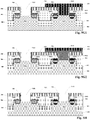
- FIGS. 5A, 5B, 5C , 5D, 5E, 5F , 5G1, 5G2, 5H , and 5I show schematic sectional views illustrating different stages of a semiconductor device manufacturing method in accordance with one or more embodiments of this present invention. This semiconductor device manufacturing method will be described in details with reference to these drawings.
- the initial structure may comprise a substrate 500 and at least one source region on the substrate 500.
- the source region may comprise a first source region 5011 for a first device and a second source region 5012 for a second device.
- the first device may be an N-type Metal Oxide Semiconductor (NMOS) transistor
- the second device may be a P-type Metal Oxide Semiconductor (PMOS) transistor.
- the first device may be a core device while the second device is an Input/Output (I/O) device.
- the initial structure may further comprise a pseudo gate structure on the source region.
- the pseudo gate structure may comprise a first pseudo gate structure on the first source region 5011, and a second pseudo gate structure on the second source region 5012.
- the first pseudo gate structure may comprise a first pseudo gate insulation layer 5021 on the first source region 5011, and a first pseudo gate electrode 5051 on the first pseudo gate insulation layer 5021.
- the second pseudo gate structure may comprise a second pseudo gate insulation layer 5022 on the second source region 5012, and a second pseudo gate electrode 5052 on the second pseudo gate insulation layer 5022.
- the initial structure may further comprise an interlayer dielectric layer 510 around the pseudo gate structure.
- the interlayer dielectric layer 510 may comprise a first part of the interlayer dielectric layer 51001 covering a portion of the first source region 5011, and a second part of the interlayer dielectric layer 51002 covering a portion of the second source region 5012.
- the upper surface of the interlayer dielectric layer 510 is on substantially the same horizontal level as the upper surface of the pseudo gate structure.
- the initial structure may further comprise a first source electrode 5071 and a first drain electrode 5081 both on the first source region 5011, a second source electrode 5072 and a second drain electrode 5082 both on the second source region 5012, a spacer 506, a third insulation layer 503, and a fourth insulation layer 504.
- These structures or components are the same as or similar to, respectively, the source electrode 307, the drain electrode 308, the spacer 306, the third insulation layer 303, and the fourth insulation layer 304 shown in Fig. 4A . Hence, in the interest of avoiding redundancy, these structures are not described in detail.
- the first pseudo gate electrode 5051 and the second pseudo gate electrode 5052 are removed to form a first cavity 5111 and a second cavity 5112, respectively. And a semiconductor structure shown in Fig. 5B is formed.
- a barrier layer 512 filling the first cavity 5111 and the second cavity 5112 is formed on the semiconductor structure of Fig. 5B through deposition or coating.
- the barrier layer 512 may, in addition to filling the first cavity 5111 and the second cavity 5112, form a layer on top of the first part of the interlayer dielectric layer 51001 and the second part of the interlayer dielectric layer 51002.
- a portion of the barrier layer 512 is removed while the remaining barrier layer 512 partially filling the first cavity 5111 and the second cavity 5112. This process exposes the upper surface of the interlayer dielectric layer 510. The portion of the barrier layer 512 that was on the first part of the interlayer dielectric layer 51001 and the second part of the interlayer dielectric layer 51002 is removed during this process.
- a loss reduction region 513 is formed in the interlayer dielectric layer 510 by conducting an ion implantation process comprising silicon ion or carbon ion on the semiconductor structure of Fig. 5D .
- the barrier layer 512 is removed.
- the pseudo gate insulation layer is removed.
- the pseudo gate insulation layer may be removed by two different processes, which will be described with reference to Figs. 5G1, 5G2, and 5H .
- the first process that can be used to remove the pseudo gate insulation layer comprises: forming a hard mask layer 531 (e.g., photoresist) on the second part of the interlayer dielectric layer 51002 and in the second cavity 5112; removing the pseudo gate insulation layer in the first cavity 5111 (the first pseudo gate insulation layer 5021) to expose a portion of the first source region 5011; and, referring to Fig. 5H , removing the hard mask layer 531.
- the first process may further comprise: conducting a thermal annealing process on the semiconductor structure with the loss reduction region after the barrier layer 512 is removed but before the hard mask layer 531 is formed.
- the second process that can be used to remove the pseudo gate insulation layer comprises: forming a cover layer 532 (e.g., a BARC layer) on the second part of the interlayer dielectric layer 51002 and in the second cavity 5112; forming a hard mask layer 533 (e.g., photoresist) on the cover layer 532; removing the pseudo gate insulation layer in the first cavity 5111 (the first pseudo gate insulation layer 5021) to expose a portion of the first source region 5011; and, referring to Fig. 5H , removing the hard mask layer 533 and the cover layer 532.
- the second process may further comprise: conducting a thermal annealing process on the semiconductor structure with the loss reduction region after the barrier layer 512 is removed but before the cover layer 532 is formed.
- the pseudo gate insulation layer in the first cavity 5111 is removed, and the pseudo gate insulation layer in the second cavity 5112 is retained. In some other embodiments, the pseudo gate insulation layer in the second cavity 5112 may also be removed.
- a gate insulation layer 521 is formed at least on the exposed portion of the first source region 5011, then a high-K dielectric layer 522 is formed on the sidewall and the base of the first cavity 5111 and the second cavity 5112, leaving an unfilled portion in each of the first cavity 5111 and the second cavity 5112.
- a gate electrode 523 is formed in the unfilled portions of the first cavity 5111 and the second cavity 5112, and on the high-K dielectric layer 522.
- the high-K dielectric layer 522 is formed on the gate insulation layer 521 in the first cavity 5111, while the high-K dielectric layer 522 is formed on the pseudo gate insulation layer (e.g., the second pseudo gate insulation layer 5022) in the second cavity 5112.
- the pseudo gate insulation layer e.g., the second pseudo gate insulation layer 5022
- the ion implantation process is conducted on at least two devices. After the ion implantation process, the pseudo gate insulation layer on at least one source region is removed, and a gate structure is formed there.
- this present invention also presents a semiconductor device.
- the source region of this semiconductor device comprises the first source region 5011 for a first device and a second source region 5012 for a second device.
- Other structures or components of this semiconductor device are the same as or similar to their counterparts in Fig. 3I , and will not be described here in the interest of avoiding redundancy.
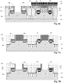
- FIGS. 6A, 6B , and 6C show schematic sectional views illustrating different stages of a semiconductor device manufacturing method in accordance with one or more embodiments of this present invention. This semiconductor device manufacturing method will be described in details with reference to these drawings.
- the barrier layer 512 is removed after the ion implantation process.
- the process to remove the barrier layer 512 may comprise, referring to Fig. 6A , removing the barrier layer 512 in the first cavity 5111 while retaining the barrier layer 512 in the second cavity 5112.
- the pseudo gate insulation layer is removed.
- the pseudo gate insulation layer may be removed by two different processes, which will be described with reference to Figs. 6B , 6C , and 5H .
- the first process that can be used to remove the pseudo gate insulation layer may comprise: forming a hard mask layer 631 (e.g., photoresist) on the second part of the interlayer dielectric layer 51002 and on the barrier layer 512 in the second cavity 5112; removing the pseudo gate insulation layer in the first cavity 5111 (the first pseudo gate insulation layer 5021) to expose a portion of the first source region 5011; and, referring to Fig. 5H , removing the hard mask layer 631 and the barrier layer 512 in the second cavity 5112.
- a hard mask layer 631 e.g., photoresist
- the second process that can be used to remove the pseudo gate insulation layer may comprise: forming a cover layer 632 (e.g., a BARC layer) on the second part of the interlayer dielectric layer 51002 and on the barrier layer 512 in the second cavity 5112; forming a hard mask layer 633 (e.g., photoresist) on the cover layer 632; removing the pseudo gate insulation layer in the first cavity 5111 (the first pseudo gate insulation layer 5021) to expose a portion of the first source region 5011; and, referring to Fig. 5H , removing the hard mask layer 633, the cover layer 632, and the barrier layer 512 in the second cavity 5112.
- a cover layer 632 e.g., a BARC layer
- a hard mask layer 633 e.g., photoresist
- a gate insulation layer 5211 is formed on at least the exposed portion of the first source region 5011, then a high-K dielectric layer 522 is formed on the sidewall and base of the first cavity 5111 and the second cavity 5112 while maintaining unfilled portions of the cavities 5111 and 5112, and a gate electrode 523 is formed to fill the previously unfilled portions of the cavities 5111, 5112 that are lined with the high-K dielectric layer 522.
- Figs. 7A, 7B , 7C, 7D , 7E , 7F, 7G1, 7G2 , 7H, and 7I show schematic sectional views illustrating different stages of a semiconductor device manufacturing method in accordance with one or more embodiments of this present invention. This semiconductor device manufacturing method will be described in details with reference to these drawings.
- This initial structure may comprise a substrate 700, a first source region 7011, a second source region 7012, a first pseudo gate insulation layer 7021, a pseudo gate electrode 7051, a second pseudo gate insulation layer 7022, and a second pseudo gate electrode 7052.
- These structures or components are the same as or similar to, respectively, the substrate 500, the first source region 5011, the second source region 5012, the first pseudo gate insulation layer 5021, the first pseudo gate electrode 5051, the second pseudo gate insulation layer 5052, and the second pseudo gate electrode 5052 of Fig. 5A , thus are not repeatedly described here.
- this initial structure may further comprise a first insulation layer 7101 around the pseudo gate structure.
- the upper surface of the first insulation layer 7101 is at substantially the same horizontal level as the upper surface of the first pseudo gate electrode 7051 and the upper surface of the second pseudo gate electrode 7052.
- the initial structure may further comprise a first source electrode 7071, a first drain electrode 7081, a second source electrode 7072, a second drain electrode 7082, a spacer 706, a third insulation layer 703, and a fourth insulation layer 704.
- first source electrode 7071, the first drain electrode 5081, the second source electrode 5072, the second drain electrode 5082, the spacer 506, the third insulation layer 503, and the fourth insulation layer 504 of Fig. 5A thus are not repeatedly described here.
- the first pseudo gate electrode 7051 and the second pseudo gate electrode 7052 are removed to form a first cavity 7111 and a second cavity 7112, respectively. And a semiconductor structure shown in Fig. 7B is formed.
- a second insulation layer 7102 is deposited on the first insulation layer 7101, on the bottom and a sidewall of the first cavity 7111, and on the bottom and a sidewall of the second cavity 7112.
- the first insulation layer 7101 and the second insulation layer 7102 together form an interlayer dielectric layer 710.
- the interlayer dielectric layer 710 may comprise a first part of the interlayer dielectric layer 71001 covering the first source region 7011, and a second part of the interlayer dielectric layer 71002 covering the second source region 7012.
- a barrier layer 712 is formed in the first cavity 7111 and the second cavity 7112.
- a loss reduction region 713 is formed in the interlayer dielectric layer 710 by conducting an ion implantation process comprising silicon ion or carbon ion on the semiconductor structure.
- the barrier layer 712 is removed.
- the pseudo gate insulation layer is removed.
- the pseudo gate insulation layer may be removed by two different processes, which will be described with reference to Figs. 7G1, 7G2 , and 7H .
- the first process that can be used to remove the pseudo gate insulation layer comprises: forming a hard mask layer 731 (e.g., photoresist) on the second part of the interlayer dielectric layer 71002 and in the second cavity 7112; removing the pseudo gate insulation layer in the first cavity 7111 (the first pseudo gate insulation layer 7021) to expose a portion of the first source region 7011; and, referring to Fig. 7H , removing the hard mask layer 731.
- the first process may further comprise: conducting a thermal annealing process on the semiconductor structure with the loss reduction region after the barrier layer 712 is removed but before the hard mask layer 731 is formed.
- the second process that can be used to remove the pseudo gate insulation layer comprises: forming a cover layer 732 (e.g., a BARC layer) on the second part of the interlayer dielectric layer 71002 and in the second cavity 7112; forming a hard mask layer 733 (e.g., photoresist) on the cover layer 732; removing the pseudo gate insulation layer in the first cavity 7111 (the first pseudo gate insulation layer 7021) to expose a portion of the first source region 7011; and, referring to Fig. 7H , removing the hard mask layer 733 and the cover layer 732.
- the second process may further comprise: conducting a thermal annealing process on the semiconductor structure with the loss reduction region after the barrier layer 712 is removed but before the cover layer 732 is formed.
- the pseudo gate insulation layer in the first cavity 7111 is removed while the pseudo gate insulation layer in the second cavity 7112 is retained. In some other embodiments, the pseudo gate insulation layer in the second cavity 7112 may also be removed.
- a gate insulation layer 721 is formed at least on the exposed portion of the first source region 7011, then a high-K dielectric layer 722 is formed in the first cavity 7111 and the second cavity 7112 along the sidewall and the base, leaving an unfilled portions in the cavities 7111, 7112.
- a gate electrode 723 is formed in the unfilled portions of the cavities 7111, 7112, and on the high-K dielectric layer 722.
- a semiconductor device manufacturing method in accordance with one or more embodiments of this present invention.
- a second insulation layer is formed on the first insulation layer, which increases the thickness of the interlayer dielectric layer and further reduces the loss of interlayer dielectric layer. Therefore the height loss of the gate electrode can be further reduced in succeeding processes.
- the ion implantation process is conducted on at least two devices. After the ion implantation process, the pseudo gate insulation layer on at least one source region is removed, and a gate structure is formed there.
- This manufacturing method reduces the loss of interlayer dielectric layer, which in turn reduces the height loss of the gate electrode.
- this manufacturing method allows a lower pseudo gate electrode and a higher gate electrode than those in conventional methods.
- the manufacturing method of this present invention provides more manufacturing margin than conventional methods and helps to improve product yield.
Landscapes
- Insulated Gate Type Field-Effect Transistor (AREA)
- Thin Film Transistor (AREA)
- Electrodes Of Semiconductors (AREA)
Abstract
Description
- This application claims priority to and benefit of Chinese Patent Application No.
201611066969.4 filed on November 29, 2016 - This present invention relates to semiconductor technology and, more specifically, to a semiconductor device and its manufacturing method.
- In conventional Metal Oxide Semiconductor Field Effect Transistor (MOSFET) manufacturing processes, a gate electrode is typically manufactured by a gate-last process, which is described below with reference to
Figs. 1A, 1B, 1C , and1D . - Referring to
Fig. 1A , asemiconductor fin 101, a Shallow Trench Isolation (STI) 102, and a well region (not shown inFig. 1A ) are first formed, then a pseudo gate structure is formed. The pseudo gate structure comprises a pseudogate insulation layer 103, apseudo gate electrode 104, and ahard mask layer 105. Thepseudo gate electrode 104 has a height of H1, as shown inFig. 1A . - Next, referring to
Fig. 1B , aspacer 106 is formed, and asource electrode 107 and adrain electrode 108 are epitaxially grown. Then an ion implantation process is conducted in thesource electrode 107 and thedrain electrode 108, asilicon nitride layer 109 covering the whole structure is formed, and an Interlayer Dielectric (ILD)layer 110 is deposited on thesilicon nitride layer 109. - Next, referring to
Fig. 1C , a planarization process is conducted on the structure ofFig. 1B to expose thepseudo gate electrode 104. - Next, referring to
Fig. 1D , thepseudo gate electrode 104 and the pseudogate insulation layer 103 are both removed to form a gate structure, which comprises agate oxide layer 111, a high-K (K is the dielectric constant)dielectric layer 112 and ametal gate electrode 113. The process to form the gate structure comprises: forming thegate oxide layer 111 through an oxidation process; depositing the high-Kdielectric layer 112 and agate material layer 113; and conducting a Chemical Mechanical Planarization (CMP) process to form the gate structure. The gate material layer may comprise a work function regulation layer and a metal layer on the work function regulation layer. In some embodiments, the process to form the gate structure may further comprise a process to pre-clean the surface of thesemiconductor fin 101 and a process to form an interlayer (IL) layer. After the gate structure is formed, themetal gate electrode 113 has a height of H2 , as shown inFig. 1D . - Next, metal contact components (not shown in the figures) connecting the metal gate electrode, the source electrode, and the drain electrode are formed.
- In the above-described manufacturing process, the metal gate electrode has a height loss of H1 -H2 , the height loss is largely due to the CMP process, the etching process, and the wet cleaning process that may be conducted in the planarization process to expose the pseudo gate electrode, the process to remove the pseudo gate electrode, the pre-clean process, and the CMP process on the gate structure.
- In actual manufacturing process, a structure with too large H1 may block the ion implantation process or cause the pseudo gate electrode to peel off; while a structure with too small H2 may have a homogeneous issue as a result of drifts or variations in the heights of different devices. For example, when H2 is too small, metal contact components may only contact the metal gate electrodes in some devices, but not in other devices. Hence, a small H1 and a large H2 are preferred in a gate manufacturing process.
- Conventional manufacturing methods have a large height loss (H1 -H2 ) in a gate electrode, thus a large H2 also requires a large H1, and a small H1 also results in a small H1.
- The inventors of this present invention investigate the large loss of the interlayer dielectric layer in conventional manufacturing methods, which leads to a large height loss of the gate electrode.
- It is an object of the present invention to propose a solution to remedy the above described issue or issues.
- The object is achieved by the features of the respective independent claims. Further embodiments and developments are defined in the dependent claims.
- This present invention provides both a semiconductor device and its manufacturing method. The present invention disclosed herein can reduce the loss of the interlayer dielectric layer in the manufacturing process and therefore reduce the height loss of the gate electrode.
- A first of the present invention provides a semiconductor device manufacturing method, comprising: providing a semiconductor structure, wherein the semiconductor structure comprises: a substrate; at least one source region on the substrate; an interlayer dielectric layer covering a portion of the source region, wherein the interlayer dielectric layer has a cavity on the source region; and a pseudo gate insulation layer at the bottom of the cavity covering a portion of the source region; forming a barrier layer in the cavity; forming a loss reduction region in the interlayer dielectric layer by conducting an ion implantation process comprising silicon ion or carbon ion on the semiconductor structure; removing the barrier layer; removing the pseudo gate insulation layer to expose a portion of the source region; and forming a gate structure on the exposed portion of the source region.
- Preferably, the ion used in the ion implantation process may comprise silicon ion, carbon ion, or an ionic group comprising silicon or carbon.
- Preferably, providing a semiconductor structure may comprise: providing an initial structure, wherein the initial structure comprises: a substrate; at least one source region on the substrate; a pseudo gate structure on the source region, wherein the pseudo gate structure comprises a pseudo gate insulation layer on the source region and a pseudo gate electrode on the pseudo gate insulation layer; and an interlayer dielectric layer around the pseudo gate structure, wherein the upper surface of the interlayer dielectric layer is on substantially the same horizontal level as the upper surface of the pseudo gate electrode; and removing the pseudo gate electrode to form a cavity.
- Preferably, the interlayer dielectric layer may comprise a first insulation layer on the source region and a second insulation layer on the first insulation layer, and providing a semiconductor structure may comprise: providing an initial structure, wherein the initial structure comprises: a substrate; at least one source region on the substrate; a pseudo gate structure on the source region, wherein the pseudo gate structure comprises a pseudo gate insulation layer on the source region and a pseudo gate electrode on the pseudo gate insulation layer; and the first insulation layer around the pseudo gate structure, wherein the upper surface of the first insulation layer is on substantially the same horizontal level as the upper surface of the pseudo gate electrode; removing the pseudo gate electrode to form a cavity; and forming the second insulation layer on the first insulation layer and on the bottom and a sidewall of the cavity, wherein the barrier layer is formed on the second insulation layer.
- Preferably, the method may further comprise removing the second insulation layer in the cavity after the barrier layer is removed but before the pseudo gate insulation layer is removed.
- Preferably, the method may further comprise conducting a thermal annealing process on the semiconductor structure with the loss reduction region after the barrier layer is removed but before the second insulation layer in the cavity is removed.
- Preferably, the gate structure may comprise: a gate insulation layer on the exposed portion of the source region; a high-K dielectric layer on the gate insulation layer; and a gate electrode on the high-K dielectric layer.
- Preferably, forming a gate structure on the exposed portion of the source region may comprise: forming a gate insulation layer on the exposed portion of the source region; forming a high-K dielectric layer on the gate insulation layer covering the semiconductor structure; forming a gate material layer on the high-K dielectric layer; and forming the gate structure by conducting a planarization process on the semiconductor structure after the gate material layer is formed.
- Preferably, the barrier layer may comprise a Bottom Anti-Reflective Coating (BARC) layer or a photoresist.
- Preferably, forming a barrier layer in the cavity may comprise: forming a barrier layer filling the cavity on the semiconductor structure; and removing a portion of the barrier layer so that the remaining barrier layer partially fills the cavity.
- Preferably, the source region may comprise a first source region for a first device and a second source region for a second device, the interlayer dielectric layer may comprise a first part of the interlayer dielectric layer covering a portion of the first source region and a second part of the interlayer dielectric layer covering a portion of the second source region, and the cavity may comprise a first cavity on the first source region and a second cavity on the second source region.
- Preferably, removing the pseudo gate insulation layer may comprise: forming a hard mask layer on the second part of the interlayer dielectric layer and in the second cavity; removing the pseudo gate insulation layer in the first cavity to expose a portion of the first source region; and removing the hard mask layer.
- Preferably, the method may further comprise conducting a thermal annealing process on the semiconductor structure with the loss reduction region after the barrier layer is removed but before the hard mask layer is formed.
- Preferably, removing the pseudo gate insulation layer may comprise: forming a cover layer on the second part of the interlayer dielectric layer and in the second cavity; forming a hard mask layer on the cover layer; removing the pseudo gate insulation layer in the first cavity to expose a portion of the first source region; and removing the hard mask layer and the cover layer.
- Preferably, the method may further comprise conducting a thermal annealing process on the semiconductor structure with the loss reduction region after the barrier layer is removed but before the cover layer is formed.
- Preferably, removing the barrier layer may comprise: removing the barrier layer in the first cavity, and wherein removing the pseudo gate insulation layer comprises: forming a hard mask layer on the second part of the interlayer dielectric layer and on the barrier layer in the second cavity; removing the pseudo gate insulation layer in the first cavity to expose a portion of the first source region; and removing the hard mask layer and the barrier layer in the second cavity.
- Preferably, removing the barrier layer may comprise: removing the barrier layer in the first cavity, and removing the pseudo gate insulation layer comprises: forming a cover layer on the second part of the interlayer dielectric layer and on the barrier layer in the second cavity; forming a hard mask layer on the cover layer; removing the pseudo gate insulation layer in the first cavity to expose a portion of the first source region; and removing the hard mask layer, the cover layer and the barrier layer in the second cavity.
- Preferably, forming a gate structure may comprise: forming a gate insulation layer on the expose portion of the first source region; forming a high-K dielectric layer in the first cavity and in the second cavity; and forming a gate electrode on the high-K dielectric layer.
- Preferably, the semiconductor structure may further comprise: a source electrode and a drain electrode in the source region and each at a side of the cavity; and a spacer on a sidewall of the cavity. Additionally, the aforementioned method may further comprise: forming a groove around the source region, and the semiconducting structure further comprises: a third insulation layer at least partially filling the groove; and a fourth insulation layer covering the third insulation layer, the source electrode, and the drain electrode, wherein the interlayer dielectric layer is formed on the fourth insulation layer.
- Preferably, the source region may be a semiconductor fin or a source region for a planar semiconductor device.
- A second aspect of the present invention provides a semiconductor device, comprising: a substrate; at least one source region on the substrate; a gate structure on the source region; an interlayer dielectric layer around the gate structure, wherein the interlayer dielectric layer has a loss reduction region formed by conducting an ion implantation process comprising silicon ion or carbon ion on the interlayer dielectric layer.
- Preferably, the gate structure may comprise: a gate insulation layer on the source region; a high-K dielectric layer on the gate insulation layer; and a gate electrode on the high-K dielectric layer.
- Preferably, the upper surface of the interlayer dielectric layer may be on substantially the same horizontal level as the upper surface of the gate electrode.
- Preferably, the interlayer dielectric layer may comprise: a first insulation layer covering a portion of the source region; and a second insulation layer on the first insulation layer. Additionally, in the aforementioned device, the source region may comprise: a first source region for a first device; and a second source region for a second device.
- Preferably, the device may further comprise: a source electrode and a drain electrode in the source region and each at a side of the gate electrode; and a spacer on the source region and located between the gate electrode and the source electrode, and between the gate electrode and the drain electrode.
- Preferably, the device may further comprise: a groove around the source region; a third insulation layer at least partially filling the groove; and a fourth insulation layer covering the third insulation layer, the source electrode, and the drain electrode, wherein the interlayer dielectric layer is formed on the fourth insulation layer.
- Preferably, the source region may be a semiconductor fin or a source region for a planar semiconductor device.
- The device according to the second aspect of the present invention may be obtained by a method according to the first aspect of the present invention.
- The drawings illustrate some embodiments of this present invention and will be used to describe this present invention along with the specification.
-
Figs. 1A, 1B, 1C , and1D show schematic sectional views illustrating different stages of a conventional MOSFET manufacturing process. -
Fig. 2 shows a flowchart illustrating a semiconductor device manufacturing method in accordance with one or more embodiments of the present invention. -
Figs. 3A, 3B, 3C ,3D, 3E, 3F ,3G, 3H, and 3I show schematic sectional views illustrating different stages of a semiconductor device manufacturing method in accordance with one or more embodiments of the present invention. -
Figs. 4A, 4B, 4C ,4D, 4E, 4F ,4G, and 4H show schematic sectional views illustrating different stages of a semiconductor device manufacturing method in accordance with one or more embodiments of this present invention. -
Figs. 5A, 5B, 5C ,5D, 5E, 5F ,5G1, 5G2, 5H , and5I show schematic sectional views illustrating different stages of a semiconductor device manufacturing method in accordance with one or more embodiments of this present invention. -
Figs. 6A, 6B , and6C show schematic sectional views illustrating different stages of a semiconductor device manufacturing method in accordance with one or more embodiments of this present invention. -
Figs. 7A, 7B ,7C, 7D ,7E ,7F, 7G1, 7G2 ,7H, and 7I show schematic sectional views illustrating different stages of a semiconductor device manufacturing method in accordance with one or more embodiments of this present invention. - Example embodiments of the present invention are described with reference to the accompanying drawings. Well known process steps and/or structures may not be described in detail, in the interest of clarity.
- The drawings and descriptions are illustrative and not restrictive. Like reference numerals may designate like (e.g., analogous or identical) elements in the specification. To the extent possible, any repetitive description will be minimized.
- Relative sizes and thicknesses of elements shown in the drawings are chosen to facilitate description and understanding, without limiting the present invention. In the drawings, the thicknesses of some layers, films, panels, regions, etc., may be exaggerated for clarity.
- Embodiments in the figures may represent idealized illustrations. Variations from the shapes illustrated may be possible, for example due to manufacturing techniques and/or tolerances. Thus, the example embodiments shall not be construed as limited to the shapes or regions illustrated herein but are to include deviations in the shapes. For example, an etched region illustrated as a rectangle may have rounded or curved features. The shapes and regions illustrated in the figures are illustrative and shall not limit the invention.
- Although the terms "first," "second," etc. may be used herein to describe various elements, these elements shall not be limited by these terms. These terms may be used to distinguish one element from another element. Thus, a first element discussed below may be termed a second element without departing from the teachings of the present present invention. The description of an element as a "first" element may not require or imply the presence of a second element or other elements. The terms "first," "second," etc. may also be used herein to differentiate different categories or sets of elements. For conciseness, the terms "first," "second," etc. may represent "first-category (or first-set)," "second-category (or second-set)," etc., respectively.
- If a first element (such as a layer, film, region, or substrate) is referred to as being "on," "neighboring," "connected to," or "coupled with" a second element, then the first element can be directly on, directly neighboring, directly connected to or directly coupled with the second element, or an intervening element may also be present between the first element and the second element. If a first element is referred to as being "directly on," "directly neighboring," "directly connected to," or "directly coupled with" a second element, then no intended intervening element (except environmental elements such as air) may also be present between the first element and the second element.
- Spatially relative terms, such as "beneath," "below," "lower," "above," "upper," and the like, may be used herein for ease of description to describe one element or feature's spatial relationship to another element(s) or feature(s) as illustrated in the figures. It will be understood that the spatially relative terms may encompass different orientations of the device in use or operation in addition to the orientation depicted in the figures. For example, if the device in the figures is turned over, elements described as "below" or "beneath" other elements or features would then be oriented "above" the other elements or features. Thus, the term "below" can encompass both an orientation of above and below. The device may be otherwise oriented (rotated 90 degrees or at other orientation), and the spatially relative descriptors used herein shall be interpreted accordingly.
- The terminology used herein is for the purpose of describing particular embodiments and is not intended to limit the present invention. As used herein, singular forms, "a," "an," and "the" may indicate plural forms as well, unless the context clearly indicates otherwise. The terms "includes" and/or "including," when used in this specification, may specify the presence of stated features, integers, steps, operations, elements, and/or components, but may not preclude the presence or addition of one or more other features, integers, steps, operations, elements, components, and/or groups.
- Unless otherwise defined, terms (including technical and scientific terms) used herein have the same meanings as what is commonly understood by one of ordinary skill in the art related to this field. Terms, such as those defined in commonly used dictionaries, shall be interpreted as having meanings that are consistent with their meanings in the context of the relevant art and shall not be interpreted in an idealized or overly formal sense unless expressly so defined herein.
- The term "connect" may mean "electrically connect." The term "insulate" may mean "electrically insulate."
- Unless explicitly described to the contrary, the word "comprise" and variations such as "comprises," "comprising," "include," or "including" may imply the inclusion of stated elements but not the exclusion of other elements.
- Various embodiments, including methods and techniques, are described in this disclosure. Embodiments of the present invention may also cover an article of manufacture that includes a non-transitory computer readable medium on which computer-readable instructions for carrying out embodiments of the inventive technique are stored. The computer readable medium may include, for example, semiconductor, magnetic, opto-magnetic, optical, or other forms of computer readable medium for storing computer readable code. Further, the present invention may also cover apparatuses for practicing embodiments of the present invention. Such apparatus may include circuits, dedicated and/or programmable, to carry out operations pertaining to embodiments of the present invention. Examples of such apparatus include a general purpose computer and/or a dedicated computing device when appropriately programmed and may include a combination of a computer/computing device and dedicated/programmable hardware circuits (such as electrical, mechanical, and/or optical circuits) adapted for the various operations pertaining to embodiments of the present invention.
-
Fig. 2 shows a flowchart illustrating a semiconductor device manufacturing method in accordance with one or more embodiments of this present invention. - In step S202, a semiconductor structure is provided. The semiconductor structure comprises a substrate, at least one source region on the substrate; an interlayer dielectric layer covering a portion of the source region, wherein the interlayer dielectric layer has a cavity on the source region; and a pseudo gate insulation layer on the bottom of the cavity covering a portion of the source region.
- In step S204, a barrier layer is formed in the cavity. For example, the barrier layer may comprise a Bottom Anti-Reflective Coating (BARC) layer or a photoresist.
- In step S206, an ion implantation process comprising silicon ion or carbon ion is conducted on the semiconductor structure to form a loss reduction region in the interlayer dielectric layer. In some embodiments, the ions that are implanted in the ion implantation process may comprise silicon ion, carbon ion, or an ionic group comprising silicon or carbon.
- In step S208, the barrier layer is removed.
- In step S210, the pseudo gate insulation layer is removed to expose a portion of the source region.
- In step 212, a gate structure is formed on the exposed portion of the source region. For example, the gate structure may comprise a gate insulation layer on the exposed portion of the source region, a high-K dielectric layer on the gate insulation layer, and a gate electrode on the high-K dielectric layer.
- In some embodiments, the gate insulation layer may comprise silicon dioxide, the high-K dielectric layer may comprise a silicon nitride, aluminum oxide (Al2O3), yttrium oxide (Y2O3), lanthanum oxide (La2O3), tantalum pentoxide (Ta2O5), titanium dioxide (TiO2), hafnium dioxide (HfO2), or zirconium dioxide (ZrO2). In some embodiments, the gate electrode may be made of a metallic material such as tungsten. The gate electrode may also comprise materials for work function regulation layer such as titanium nitride, tantalum nitride, or titanium aluminum alloy.
- In the above-described embodiments of this present invention, a loss reduction region is formed in the interlayer dielectric layer by conducting an ion implantation process comprising silicon ion or carbon ion on the semiconductor structure, the loss reduction region can reduce the loss of interlayer dielectric layer, and reduce the height loss of the gate electrode, in the succeeding stages that involve an etching or a planarization process (for example, step S210 may involve an etching process and step S212 may involve a planarization process). Thus, this present invention allows a lower pseudo gate electrode and a higher gate electrode than those in conventional methods. Hence the manufacturing method of this present invention provides more manufacture margin than conventional methods and helps to improve production yield.
- In the embodiments of this present invention, the source region may be either a semiconductor fin or a source region for a planar device. That it, this present invention can apply to either a fin-type semiconductor device or a planar semiconductor device. For conciseness, this present invention will be described using only examples where the source region is a semiconductor fin.
-
Figs. 3A, 3B, 3C ,3D, 3E, 3F ,3G, 3H, and 3I show schematic sectional views illustrating different stages of a semiconductor device manufacturing method in accordance with one or more embodiments of this present invention. This semiconductor device manufacturing method will be described in details with reference to these drawings. -
Figs. 3A and 3B show schematic sectional views illustrating two stages of this semiconducting manufacturing method corresponding to step S202. - Referring to
Fig. 3A , an initial structure is first provided. This initial structure may comprise a substrate 300 (e.g., a silicon substrate) and at least one source region 301 (e.g., a semiconductor fin) on thesubstrate 300. The initial structure may further comprise a pseudo gate structure on thesource region 301. The pseudo gate structure may comprise a pseudo gate insulation layer 302 (e.g., a silicon dioxide layer) on thesource region 301, and a pseudo gate electrode 305 (e.g., polycrystalline silicon) on the pseudogate insulation layer 302. The initial structure may further comprise an interlayer dielectric layer 310 (e.g., a silicon dioxide layer) around the pseudo gate structure. The upper surface of theinterlayer dielectric layer 310 is on substantially the same horizontal level as the upper surface of thepseudo gate electrode 305. - In the above description, "substantially the same" means that the horizontal difference between the upper surface of the
interlayer dielectric layer 310 and the upper surface of thepseudo gate electrode 305 is within an acceptable range, For example, the upper surface of theinterlayer dielectric layer 310 and the upper surface of thepseudo gate electrode 305 may be made at "substantially the same" horizontal level by a same planarization process. This present invention is not limited herein though. Additionally, the dash lines in the drawings serve for an illustrative purpose to distinguish different regions only, and do not represent any structural components in the devices. - Referring to
Fig. 3A , optionally, the initial structure may further comprise asource electrode 307 and adrain electrode 308 in thesource region 301 and each at a side of the pseudo gate structure. The initial structure may further comprise aspacer 306 on thesource region 301 and located between thesource electrode 307 and thepseudo gate electrode 305, and between thedrain electrode 308 and thepseudo gate electrode 305. For example, thespacer 306 may comprise silicon dioxide or silicon nitride. In one embodiment, a groove may be formed around thesource region 301, and, optionally, the initial structure may further comprise a third insulation layer 303 (e.g., a silicon dioxide layer) at least partially filling the groove, a fourth insulation layer 304 (e.g., a silicon nitride layer) covering thethird insulation layer 303, thesource electrode 307, and thedrain electrode 308, wherein theinterlayer dielectric layer 310 is formed onfourth insulation layer 304. - Next, referring to
Fig. 3B , thepseudo gate electrode 305 is removed to form acavity 311, and a semiconductor structure corresponding to step S202 is formed. This semiconductor structure comprises asubstrate 300 and at least onesource region 301 on thesubstrate 300. This semiconductor structure may further comprise aninterlayer dielectric layer 310 partially covering thesource region 301, wherein theinterlayer dielectric layer 310 has acavity 311 on thesource region 301. This semiconductor structure may further comprise a pseudogate insulation layer 302 at the bottom of thecavity 311 covering a portion thesource region 301. - Referring to
Fig. 3B , optionally, this semiconductor structure may further comprise asource electrode 307 and adrain electrode 308 in thesource region 301 and each at a side of thecavity 311. This semiconductor structure may further comprise aspacer 306 on a sidewall of thecavity 311. In one embodiment, a groove may be formed around thesource region 301, and, optionally, this semiconductor structure may further comprise athird insulation layer 303 at least partially filling the groove, afourth insulation layer 304 covering thethird insulation layer 303, thesource electrode 307, and thedrain electrode 308, wherein theinterlayer dielectric layer 310 is formed on thefourth insulation layer 304. - Next, a barrier layer is formed in the cavity. Referring to
Fig. 3C , in one embodiment, the process to form the barrier layer comprises: forming abarrier layer 312 filling thecavity 311 on the semiconductor structure through deposition or coating. Referring toFig. 3D , optionally, the process to form the barrier layer may further comprise removing a portion of thebarrier layer 312 so that the remainingbarrier layer 312 partially fills thecavity 311, and the upper surface of theinterlayer dielectric layer 310 is exposed. - Next, referring to
Fig. 3E , aloss reduction region 313 is formed in theinterlayer dielectric layer 310 by conducting an ion implantation process comprising silicon ion or carbon ion on the semiconductor structure. For example, the ion used in the ion implantation process may comprise silicon ion, carbon ion, or an ionic group comprising silicon or carbon. In one embodiment, the energy for the ion implantation process is in a range of 1 KeV to 10 KeV (e.g., 5 KeV). The implantation dose may be in a range of 1×10¹² atom/cm2 to 1×10¹⁶ atom/cm2 - Silicon or carbon implanted into the
interlayer dielectric layer 310 can reduce the loss of theinterlayer dielectric layer 310 in succeeding etching or planarization processes, and thus reduces the height loss of the gate electrode. Additionally, thebarrier layer 312 formed on thesource region 301 can prevent silicon ion, carbon ion, or an ionic group comprising silicon or carbon from being implanted into thesource region 301 in the ion implantation process. - In some embodiments, the ion implantation process may also implant the ions into the
spacer 106 and/or thefourth insulation layer 304, thus form a loss reduction region in those regions as well. However, since thespacer 106 and thefourth insulation layer 304 are thinner than theinterlayer dielectric layer 310, the loss reduction region formed in these regions has a less loss reduction effect than that formed in theinterlayer dielectric layer 310. Therefore, the loss reduction region in thespacer 106 and thefourth insulation layer 304 is not shown in the drawing. However, a person of ordinary skill in the art in this field would understand that, in some embodiments, a loss reduction region may also be formed in thespacer 106 and/or thefourth insulation layer 304. - Next, referring to
Fig. 3F , thebarrier layer 312 is removed. For example, thebarrier layer 312 may be removed by an etching process that has a high etch selectivity ratio to silicon oxide or silicon nitride, such as Reactive Ion Etching (RIE) or wet etching. - Next, referring to
Fig. 3G , the pseudogate insulation layer 302 is removed by an etching process to expose a portion of thesource region 301. - Next, a gate structure is formed on the exposed portion of the
source region 301. Referring toFig. 3H , in one embodiment, the process to form the gate structure may comprise: forming a gate insulation layer 321 (e.g., a silicon dioxide layer) on the exposed portion of thesource region 301 through a deposition or an oxidation process; forming a high-K dielectric layer 322 on thegate insulation layer 321 covering the semiconductor structure; and forming agate material layer 323 on the high-K dielectric layer 322. Referring toFig. 3I , optionally, the process to form the gate structure may further comprise: forming agate structure 320 by conducting a planarization process on the semiconductor structure after thegate material layer 323 is formed. - This concludes the description of a semiconductor device manufacturing method in accordance with one or more embodiments of this present invention. In this manufacturing method, a loss reduction region is formed in the interlayer dielectric layer by conducting an ion implantation process comprising silicon ion or carbon ion. The loss reduction region can reduce the loss of the interlayer dielectric layer in the succeeding etching or planarization processes, and thus reduce the height loss of the gate electrode. Hence this manufacturing method provides more manufacture margin than conventional methods and helps to improve production yield.
- Based on the manufacturing method described above, this present invention also presents a semiconductor device. Referring to
Fig. 3I , this semiconductor device comprises asubstrate 300 and at least onesource region 301 on thesubstrate 300. This semiconductor device may further comprise agate structure 320 on thesource region 301, and aninterlayer dielectric layer 310 around thegate structure 320. Theinterlayer dielectric layer 310 has aloss reduction region 313 that is formed by ion implanting silicon or carbon ions into theinterlayer dielectric layer 310. That is, theloss reduction region 313 comprise silicon or carbon. - Referring to
Fig. 3I , in one embodiment, thegate structure 320 comprises: agate insulation layer 321 on thesource region 301, a high-K dielectric layer 322 on thegate insulation layer 321, and agate electrode 323 on the high-K dielectric layer 322. - Referring to
Fig. 3I , in one embodiment, the upper surface of theinterlayer dielectric layer 310 is on substantially the same horizontal level as the upper surface of thegate electrode 323. - Referring to
Fig. 3I , in one embodiment, the semiconductor device may further comprise: asource electrode 307 and adrain electrode 308 in thesource region 301 and each at a side of thegate electrode 323. In one embodiment, the semiconductor device may further comprise aspacer 306 on thesource region 301 and located between thegate electrode 323 and thesource electrode 307, and between thegate electrode 323 and thedrain electrode 308. - Referring to
Fig. 3I , in one embodiment, a groove is formed around thesource region 301. And the semiconductor device may further comprise athird insulation layer 303 at least partially filling the groove. In one embodiment, the semiconductor device may further comprise afourth insulation layer 304 covering thethird insulation layer 303, thesource electrode 307, and thedrain electrode 308, and theinterlayer dielectric layer 310 is on thefourth dielectric layer 304. - In the embodiment of this present invention, the
source region 301 may be a semiconductor fin or a source region of a planar device. -
Figs. 4A, 4B, 4C ,4D, 4E, 4F ,4G, and 4H show schematic sectional views illustrating different stages of a semiconductor device manufacturing method in accordance with one or more embodiments of this present invention. This semiconductor device manufacturing method will be described in details with reference to these drawings. - Referring to
Fig. 4A , an initial structure is first provided. This initial structure may comprise asubstrate 400 and at least onesource region 401 on thesubstrate 400. The initial structure may further comprise a pseudo gate structure on thesource region 401. The pseudo gate structure may comprise a pseudogate insulation layer 402 on thesource region 401, and apseudo gate electrode 405 on the pseudogate insulation layer 402. The initial structure may further comprise a first insulation layer 4101 (e.g., a silicon dioxide layer) around the pseudo gate structure. The upper surface of thefirst insulation layer 4101 is on substantially the same horizontal level as the upper surface of thepseudo gate electrode 405. - In some embodiments, the initial structure may further comprise a
source electrode 407, adrain electrode 408, aspacer 406, athird insulation layer 403, and afourth insulation layer 404. These structures or components are the same as or similar to, respectively, thesource electrode 307, thedrain electrode 308, thespacer 306, thethird insulation layer 303, and thefourth insulation layer 304 shown inFig. 3A , thus are not repeatedly described here. - Next, referring to
Fig. 4B , thepseudo gate electrode 405 is removed to form acavity 411. - Next, referring to
Fig. 4C , asecond insulation layer 4102 is formed by a deposition method (e.g., Atomic Layer Deposition (ALD)) on thefirst insulation layer 4101 and on the bottom and the sidewall of thecavity 411. Thesecond insulation layer 4102 may comprise silicon dioxide or silicon nitride. In one embodiment, a portion of thefirst insulation layer 4101 and a portion of thesecond insulation layer 4102 may together form aninterlayer dielectric layer 410. That is, theinterlayer dielectric layer 410 comprises a portion of thefirst insulation layer 4101 covering thesource region 401 and a portion of thesecond insulation layer 4102 on that portion of thefirst insulation layer 4101. - This concludes the description of the semiconductor structure shown in
Fig. 4C . This semiconductor structure is similar to the semiconductor structure shown inFig. 3B . The difference between these two semiconductor structures is that the interlayer dielectric layer shown inFig. 3B has a single layer structure while the interlayer dielectric layer shown inFig. 4C has a multi-layer structure (e.g., two-layer structure). - Next, referring to
Fig. 4D , abarrier layer 412 is formed in thecavity 411. Thebarrier layer 412 is formed on thesecond insulation layer 4102. - Next, referring to
Fig. 4E , aloss reduction region 413 is formed in theinterlayer dielectric layer 410 by conducting an ion implantation process comprising silicon ion or carbon ion on the semiconductor structure. In one embodiment, theloss reduction region 413 is formed in thesecond insulation layer 4102. In another embodiment, theloss reduction region 413 may also be formed in thefirst insulation layer 4101. - Next, referring to
Fig. 4F , thebarrier layer 412 is removed. After thebarrier layer 412 is removed, thesecond insulation layer 4102 in thecavity 411 is also removed. - In one embodiment, the manufacturing method may further comprise conducting a thermal annealing process on the semiconductor structure after the
barrier layer 412 is removed but before thesecond insulation layer 4102 in thecavity 411 is removed. The temperature for the thermal annealing process may be in a range of 500°C to 1200°C (e.g., 800°C). The thermal annealing process can repair the damage in the semiconductor structure made in the ion implantation process. - Next, referring to
Fig. 4G , the pseudogate insulation layer 402 is removed to expose a portion of thesource region 401. - Next, referring to
Fig. 4H , agate structure 420 is formed on the exposed portion of thesource region 401. Thegate structure 420 may comprise agate insulation layer 421 on thesource region 401, a high-K dielectric layer 422 on thegate insulation layer 421, and agate electrode 423 on the high-K dielectric layer 422. - This concludes the description of a semiconductor device manufacturing method in accordance with one or more embodiments of this present invention. In this manufacturing method, a second insulation layer is formed on the first insulation layer, which increases the thickness of the interlayer dielectric layer and further reduces the loss of interlayer dielectric layer. Therefore the height decrease of the gate electrode can be further avoided in succeeding processes. This manufacturing method provides more manufacturing margin than conventional methods and helps to improve production yield.
- In some embodiments, the process to form the second insulation layer may be repeated multiple times. For example, referring to
Fig. 4F , after thebarrier layer 412 andsecond insulation layer 4102 in thecavity 411 have been removed, a new second insulation layer may be formed on the semiconductor structure ofFig. 4F , a new barrier layer may be formed on the new second insulation layer, and an ion implantation process may be conducted on the semiconductor structure again. After that, the new barrier layer and the new second insulation layer in the cavity will be removed again and this process may be repeated multiple times until the thickness of the second insulation layer meets a predefined criterion. This repeated process may form a thick second insulation layer that can further reduce the loss of the interlayer dielectric layer. In some embodiment, this repeated process can also increase the thickness of the interlayer dielectric layer. - Based on the manufacturing method described above, this present invention further presents a semiconductor device, as shown in
Fig. 4H . Most of the structures in the semiconductor device shown inFig. 4H are the same as or similar to their counterparts in the semiconductor device shown inFig. 3I , therefore are not repeatedly described here. The difference between these two semiconductor devices is that the interlayer dielectric layer shown inFig. 3I has a single layer structure while the interlayer dielectric layer shown inFig. 4H has a multi-layer structure (e.g., a two-layer structure). Referring toFig. 4H , in one embodiment, theinterlayer dielectric layer 410 may comprise a portion of thefirst insulation layer 4101 on thesource region 401, and a portion of thesecond insulation layer 4102 on that portion of thefirst insulation layer 4101. Thefirst insulation layer 4101 may comprise silicon dioxide, and thesecond insulation layer 4102 may comprise silicon dioxide or silicon nitride. -
Figs. 5A, 5B, 5C ,5D, 5E, 5F ,5G1, 5G2, 5H , and5I show schematic sectional views illustrating different stages of a semiconductor device manufacturing method in accordance with one or more embodiments of this present invention. This semiconductor device manufacturing method will be described in details with reference to these drawings. - Referring to
Fig. 5A , an initial structure is first provided. The initial structure may comprise asubstrate 500 and at least one source region on thesubstrate 500. For example, the source region may comprise afirst source region 5011 for a first device and asecond source region 5012 for a second device. In one embodiment, the first device may be an N-type Metal Oxide Semiconductor (NMOS) transistor, and the second device may be a P-type Metal Oxide Semiconductor (PMOS) transistor. In another embodiment, the first device may be a core device while the second device is an Input/Output (I/O) device. - Referring to
Fig. 5A , the initial structure may further comprise a pseudo gate structure on the source region. For example, the pseudo gate structure may comprise a first pseudo gate structure on thefirst source region 5011, and a second pseudo gate structure on thesecond source region 5012. The first pseudo gate structure may comprise a first pseudogate insulation layer 5021 on thefirst source region 5011, and a firstpseudo gate electrode 5051 on the first pseudogate insulation layer 5021. The second pseudo gate structure may comprise a second pseudogate insulation layer 5022 on thesecond source region 5012, and a secondpseudo gate electrode 5052 on the second pseudogate insulation layer 5022. - Referring to
Fig. 5A , the initial structure may further comprise aninterlayer dielectric layer 510 around the pseudo gate structure. Theinterlayer dielectric layer 510 may comprise a first part of theinterlayer dielectric layer 51001 covering a portion of thefirst source region 5011, and a second part of theinterlayer dielectric layer 51002 covering a portion of thesecond source region 5012. The upper surface of theinterlayer dielectric layer 510 is on substantially the same horizontal level as the upper surface of the pseudo gate structure. - Additionally, the initial structure may further comprise a
first source electrode 5071 and afirst drain electrode 5081 both on thefirst source region 5011, asecond source electrode 5072 and asecond drain electrode 5082 both on thesecond source region 5012, aspacer 506, athird insulation layer 503, and afourth insulation layer 504. These structures or components are the same as or similar to, respectively, thesource electrode 307, thedrain electrode 308, thespacer 306, thethird insulation layer 303, and thefourth insulation layer 304 shown inFig. 4A . Hence, in the interest of avoiding redundancy, these structures are not described in detail. - Next, referring to
Fig. 5B , the firstpseudo gate electrode 5051 and the secondpseudo gate electrode 5052 are removed to form afirst cavity 5111 and asecond cavity 5112, respectively. And a semiconductor structure shown inFig. 5B is formed. - Next, referring to
Fig. 5C , abarrier layer 512 filling thefirst cavity 5111 and thesecond cavity 5112 is formed on the semiconductor structure ofFig. 5B through deposition or coating. As shown inFig. 5C , thebarrier layer 512 may, in addition to filling thefirst cavity 5111 and thesecond cavity 5112, form a layer on top of the first part of theinterlayer dielectric layer 51001 and the second part of theinterlayer dielectric layer 51002. - Next, referring to
Fig. 5D , a portion of thebarrier layer 512 is removed while the remainingbarrier layer 512 partially filling thefirst cavity 5111 and thesecond cavity 5112. This process exposes the upper surface of theinterlayer dielectric layer 510. The portion of thebarrier layer 512 that was on the first part of theinterlayer dielectric layer 51001 and the second part of theinterlayer dielectric layer 51002 is removed during this process. - Next, referring to
Fig. 5E , aloss reduction region 513 is formed in theinterlayer dielectric layer 510 by conducting an ion implantation process comprising silicon ion or carbon ion on the semiconductor structure ofFig. 5D . - Next, referring to
Fig. 5F , thebarrier layer 512 is removed. - Next, the pseudo gate insulation layer is removed. The pseudo gate insulation layer may be removed by two different processes, which will be described with reference to
Figs. 5G1, 5G2, and 5H . - Referring to
Fig. 5G1 , in one embodiment, the first process that can be used to remove the pseudo gate insulation layer comprises: forming a hard mask layer 531 (e.g., photoresist) on the second part of theinterlayer dielectric layer 51002 and in thesecond cavity 5112; removing the pseudo gate insulation layer in the first cavity 5111 (the first pseudo gate insulation layer 5021) to expose a portion of thefirst source region 5011; and, referring toFig. 5H , removing thehard mask layer 531. In one embodiment, the first process may further comprise: conducting a thermal annealing process on the semiconductor structure with the loss reduction region after thebarrier layer 512 is removed but before thehard mask layer 531 is formed. - Referring to
Fig. 5G2 , in another embodiment, the second process that can be used to remove the pseudo gate insulation layer comprises: forming a cover layer 532 (e.g., a BARC layer) on the second part of theinterlayer dielectric layer 51002 and in thesecond cavity 5112; forming a hard mask layer 533 (e.g., photoresist) on thecover layer 532; removing the pseudo gate insulation layer in the first cavity 5111 (the first pseudo gate insulation layer 5021) to expose a portion of thefirst source region 5011; and, referring toFig. 5H , removing thehard mask layer 533 and thecover layer 532. In one embodiment, the second process may further comprise: conducting a thermal annealing process on the semiconductor structure with the loss reduction region after thebarrier layer 512 is removed but before thecover layer 532 is formed. - In the above-described embodiments, the pseudo gate insulation layer in the
first cavity 5111 is removed, and the pseudo gate insulation layer in thesecond cavity 5112 is retained. In some other embodiments, the pseudo gate insulation layer in thesecond cavity 5112 may also be removed. - Next, referring to
Fig. 5I , after the pseudo gate insulation layer in thefirst cavity 5111 is removed, agate insulation layer 521 is formed at least on the exposed portion of thefirst source region 5011, then a high-K dielectric layer 522 is formed on the sidewall and the base of thefirst cavity 5111 and thesecond cavity 5112, leaving an unfilled portion in each of thefirst cavity 5111 and thesecond cavity 5112. Agate electrode 523 is formed in the unfilled portions of thefirst cavity 5111 and thesecond cavity 5112, and on the high-K dielectric layer 522. In this embodiment, the high-K dielectric layer 522 is formed on thegate insulation layer 521 in thefirst cavity 5111, while the high-K dielectric layer 522 is formed on the pseudo gate insulation layer (e.g., the second pseudo gate insulation layer 5022) in thesecond cavity 5112. - This concludes the description of a semiconductor device manufacturing method in accordance with one or more embodiments of this present invention. In this method, the ion implantation process is conducted on at least two devices. After the ion implantation process, the pseudo gate insulation layer on at least one source region is removed, and a gate structure is formed there.
- Based on the manufacturing method described above, this present invention also presents a semiconductor device. Referring to
Fig. 5I , the source region of this semiconductor device comprises thefirst source region 5011 for a first device and asecond source region 5012 for a second device. Other structures or components of this semiconductor device are the same as or similar to their counterparts inFig. 3I , and will not be described here in the interest of avoiding redundancy. -
Figs. 6A, 6B , and6C show schematic sectional views illustrating different stages of a semiconductor device manufacturing method in accordance with one or more embodiments of this present invention. This semiconductor device manufacturing method will be described in details with reference to these drawings. - Referring to
Fig. 5E , thebarrier layer 512 is removed after the ion implantation process. In some embodiments, the process to remove thebarrier layer 512 may comprise, referring toFig. 6A , removing thebarrier layer 512 in thefirst cavity 5111 while retaining thebarrier layer 512 in thesecond cavity 5112. - Next, the pseudo gate insulation layer is removed. The pseudo gate insulation layer may be removed by two different processes, which will be described with reference to
Figs. 6B ,6C , and5H . - Referring to
Fig. 6B , in one embodiment, the first process that can be used to remove the pseudo gate insulation layer may comprise: forming a hard mask layer 631 (e.g., photoresist) on the second part of theinterlayer dielectric layer 51002 and on thebarrier layer 512 in thesecond cavity 5112; removing the pseudo gate insulation layer in the first cavity 5111 (the first pseudo gate insulation layer 5021) to expose a portion of thefirst source region 5011; and, referring toFig. 5H , removing thehard mask layer 631 and thebarrier layer 512 in thesecond cavity 5112. - Referring to
Fig. 6C , in another embodiment, the second process that can be used to remove the pseudo gate insulation layer may comprise: forming a cover layer 632 (e.g., a BARC layer) on the second part of theinterlayer dielectric layer 51002 and on thebarrier layer 512 in thesecond cavity 5112; forming a hard mask layer 633 (e.g., photoresist) on thecover layer 632; removing the pseudo gate insulation layer in the first cavity 5111 (the first pseudo gate insulation layer 5021) to expose a portion of thefirst source region 5011; and, referring toFig. 5H , removing thehard mask layer 633, thecover layer 632, and thebarrier layer 512 in thesecond cavity 5112. - Next, referring to
Fig. 5I , after the pseudo gate insulation layer in thefirst cavity 5111 is removed, a gate insulation layer 5211 is formed on at least the exposed portion of thefirst source region 5011, then a high-K dielectric layer 522 is formed on the sidewall and base of thefirst cavity 5111 and thesecond cavity 5112 while maintaining unfilled portions of thecavities gate electrode 523 is formed to fill the previously unfilled portions of thecavities K dielectric layer 522. - This concludes the description of a semiconductor manufacturing method in accordance with one or more embodiments of this present invention. In this method, after the ion implantation process, the pseudo gate insulation layer on at least one source region is removed, and a gate structure is formed there.
-
Figs. 7A, 7B ,7C, 7D ,7E ,7F, 7G1, 7G2 ,7H, and 7I show schematic sectional views illustrating different stages of a semiconductor device manufacturing method in accordance with one or more embodiments of this present invention. This semiconductor device manufacturing method will be described in details with reference to these drawings. - Referring to
Fig. 7A , an initial structure is first provided. This initial structure may comprise asubstrate 700, afirst source region 7011, asecond source region 7012, a first pseudogate insulation layer 7021, apseudo gate electrode 7051, a second pseudogate insulation layer 7022, and a secondpseudo gate electrode 7052. These structures or components are the same as or similar to, respectively, thesubstrate 500, thefirst source region 5011, thesecond source region 5012, the first pseudogate insulation layer 5021, the firstpseudo gate electrode 5051, the second pseudogate insulation layer 5052, and the secondpseudo gate electrode 5052 ofFig. 5A , thus are not repeatedly described here. - Referring to
Fig. 7A , this initial structure may further comprise afirst insulation layer 7101 around the pseudo gate structure. The upper surface of thefirst insulation layer 7101 is at substantially the same horizontal level as the upper surface of the firstpseudo gate electrode 7051 and the upper surface of the secondpseudo gate electrode 7052. - Additionally, the initial structure may further comprise a
first source electrode 7071, afirst drain electrode 7081, asecond source electrode 7072, asecond drain electrode 7082, aspacer 706, athird insulation layer 703, and afourth insulation layer 704. These structures or components are the same as or similar to, respectively, thefirst source electrode 5071, thefirst drain electrode 5081, thesecond source electrode 5072, thesecond drain electrode 5082, thespacer 506, thethird insulation layer 503, and thefourth insulation layer 504 ofFig. 5A , thus are not repeatedly described here. - Next, referring to
Fig. 7B , the firstpseudo gate electrode 7051 and the secondpseudo gate electrode 7052 are removed to form afirst cavity 7111 and asecond cavity 7112, respectively. And a semiconductor structure shown inFig. 7B is formed. - Next, referring to
Fig. 7C , asecond insulation layer 7102 is deposited on thefirst insulation layer 7101, on the bottom and a sidewall of thefirst cavity 7111, and on the bottom and a sidewall of thesecond cavity 7112. Thefirst insulation layer 7101 and thesecond insulation layer 7102 together form aninterlayer dielectric layer 710. Theinterlayer dielectric layer 710 may comprise a first part of theinterlayer dielectric layer 71001 covering thefirst source region 7011, and a second part of theinterlayer dielectric layer 71002 covering thesecond source region 7012. - Next, referring to
Fig. 7D , abarrier layer 712 is formed in thefirst cavity 7111 and thesecond cavity 7112. - Next, referring to
Fig. 7E , aloss reduction region 713 is formed in theinterlayer dielectric layer 710 by conducting an ion implantation process comprising silicon ion or carbon ion on the semiconductor structure. - Next, referring to
Fig. 7F , thebarrier layer 712 is removed. - Next, the pseudo gate insulation layer is removed. The pseudo gate insulation layer may be removed by two different processes, which will be described with reference to
Figs. 7G1, 7G2 , and7H . - Referring to
Fig. 7G1 , in one embodiment, the first process that can be used to remove the pseudo gate insulation layer comprises: forming a hard mask layer 731 (e.g., photoresist) on the second part of theinterlayer dielectric layer 71002 and in thesecond cavity 7112; removing the pseudo gate insulation layer in the first cavity 7111 (the first pseudo gate insulation layer 7021) to expose a portion of thefirst source region 7011; and, referring toFig. 7H , removing thehard mask layer 731. In one embodiment, the first process may further comprise: conducting a thermal annealing process on the semiconductor structure with the loss reduction region after thebarrier layer 712 is removed but before thehard mask layer 731 is formed. - Referring to
Fig. 7G2 , in another embodiment, the second process that can be used to remove the pseudo gate insulation layer comprises: forming a cover layer 732 (e.g., a BARC layer) on the second part of theinterlayer dielectric layer 71002 and in thesecond cavity 7112; forming a hard mask layer 733 (e.g., photoresist) on thecover layer 732; removing the pseudo gate insulation layer in the first cavity 7111 (the first pseudo gate insulation layer 7021) to expose a portion of thefirst source region 7011; and, referring toFig. 7H , removing thehard mask layer 733 and thecover layer 732. In one embodiment, the second process may further comprise: conducting a thermal annealing process on the semiconductor structure with the loss reduction region after thebarrier layer 712 is removed but before thecover layer 732 is formed. - In the above-described embodiments, the pseudo gate insulation layer in the
first cavity 7111 is removed while the pseudo gate insulation layer in thesecond cavity 7112 is retained. In some other embodiments, the pseudo gate insulation layer in thesecond cavity 7112 may also be removed. - Next, referring to
Fig. 7I , after the pseudo gate insulation layer in thefirst cavity 7111 is removed, agate insulation layer 721 is formed at least on the exposed portion of thefirst source region 7011, then a high-K dielectric layer 722 is formed in thefirst cavity 7111 and thesecond cavity 7112 along the sidewall and the base, leaving an unfilled portions in thecavities gate electrode 723 is formed in the unfilled portions of thecavities K dielectric layer 722. - This concludes the description of a semiconductor device manufacturing method in accordance with one or more embodiments of this present invention. In this manufacturing method, a second insulation layer is formed on the first insulation layer, which increases the thickness of the interlayer dielectric layer and further reduces the loss of interlayer dielectric layer. Therefore the height loss of the gate electrode can be further reduced in succeeding processes. Additionally, in this manufacturing method, the ion implantation process is conducted on at least two devices. After the ion implantation process, the pseudo gate insulation layer on at least one source region is removed, and a gate structure is formed there.
- This manufacturing method reduces the loss of interlayer dielectric layer, which in turn reduces the height loss of the gate electrode. Thus, this manufacturing method allows a lower pseudo gate electrode and a higher gate electrode than those in conventional methods. Hence, the manufacturing method of this present invention provides more manufacturing margin than conventional methods and helps to improve product yield.
- This concludes the description of a semiconductor device and its manufacturing method in accordance with one or more embodiments of this present invention. For the purpose of conciseness and convenience, some components or procedures that are well known to one of ordinary skill in the art in this field are omitted. These omissions, however, do not prevent one of ordinary skill in the art in this field to make and use the present invention herein disclosed.
Claims (15)
- A semiconductor device manufacturing method, comprising:providing a semiconductor structure, wherein the semiconductor structure comprises:a substrate;at least one source region on the substrate;an interlayer dielectric layer covering a portion of the source region, wherein the interlayer dielectric layer has a cavity on the source region; anda pseudo gate insulation layer at the bottom of the cavity covering a portion of the source region;forming a barrier layer in the cavity;forming a loss reduction region in the interlayer dielectric layer by conducting an ion implantation process comprising silicon ion or carbon ion on the semiconductor structure;removing the barrier layer;removing the pseudo gate insulation layer to expose a portion of the source region; andforming a gate structure on the exposed portion of the source region; andwherein preferably: the source region is a semiconductor fin or a source region for a planar semiconductor device.
- The method of claim 1, wherein
the ion used in the ion implantation process comprises silicon ion, carbon ion, or an ionic group comprising silicon or carbon; and/or
the barrier layer comprises a Bottom Anti-Reflective Coating, BARC, layer or a photoresist. - The method of claim 1 or 2, wherein providing a semiconductor structure comprises:providing an initial structure, wherein the initial structure comprises:a substrate;at least one source region on the substrate;a pseudo gate structure on the source region, wherein the pseudo gate structure comprises a pseudo gate insulation layer on the source region and a pseudo gate electrode on the pseudo gate insulation layer; andan interlayer dielectric layer around the pseudo gate structure, wherein the upper surface of the interlayer dielectric layer is on substantially the same horizontal level as the upper surface of the pseudo gate electrode; andremoving the pseudo gate electrode to form a cavity.
- The method of any one of the claims 1-3, wherein the interlayer dielectric layer comprises a first insulation layer on the source region and a second insulation layer on the first insulation layer, and wherein providing a semiconductor structure comprises:providing an initial structure, wherein the initial structure comprises:a substrate;at least one source region on the substrate;a pseudo gate structure on the source region, wherein the pseudo gate structure comprises a pseudo gate insulation layer on the source region and a pseudo gate electrode on the pseudo gate insulation layer; andthe first insulation layer around the pseudo gate structure, wherein the upper surface of the first insulation layer is on substantially the same horizontal level as the upper surface of the pseudo gate electrode;removing the pseudo gate electrode to form a cavity; andforming the second insulation layer on the first insulation layer and on the bottom and a sidewall of the cavity, wherein the barrier layer is formed on the second insulation layer; andwherein the method, preferably, further comprises: removing the second insulation layer in the cavity after the barrier layer is removed but before the pseudo gate insulation layer is removed, wherein, preferably, a thermal annealing process is conducted on the semiconductor structure with the loss reduction region after the barrier layer is removed but before the second insulation layer in the cavity is removed.
- The method of any one of the claims 1-4, wherein the gate structure comprises:a gate insulation layer on the exposed portion of the source region;a high-K dielectric layer on the gate insulation layer; anda gate electrode on the high-K dielectric layer; andwherein preferably: forming a gate structure on the exposed portion of the source region comprises:forming a gate insulation layer on the exposed portion of the source region;forming a high-K dielectric layer on the gate insulation layer covering the semiconductor structure;forming a gate material layer on the high-K dielectric layer; andforming the gate structure by conducting a planarization process on the semiconductor structure after the gate material layer is formed.
- The method of any one of the claims 1-5, wherein forming a barrier layer in the cavity comprises:forming a barrier layer filling the cavity on the semiconductor structure; andremoving a portion of the barrier layer so that the remaining barrier layer partially fills the cavity.
- The method of any one of the claims 1-6, wherein the source region comprises a first source region for a first device and a second source region for a second device, wherein the interlayer dielectric layer comprises a first part of the interlayer dielectric layer covering a portion of the first source region and a second part of the interlayer dielectric layer covering a portion of the second source region, and wherein the cavity comprises a first cavity on the first source region and a second cavity on the second source region.
- The method of claim 7, wherein
removing the pseudo gate insulation layer comprises: forming a hard mask layer on the second part of the interlayer dielectric layer and in the second cavity; removing the pseudo gate insulation layer in the first cavity to expose a portion of the first source region; and removing the hard mask layer. - The method of claim 8, wherein
the method further comprises: conducting a thermal annealing process on the semiconductor structure with the loss reduction region after the barrier layer is removed but before the hard mask layer is formed; and/or
forming a gate structure comprises: forming a gate insulation layer on the expose portion of the first source region; forming a high-K dielectric layer in the first cavity and in the second cavity; and forming a gate electrode on the high-K dielectric layer. - The method of claim 7, wherein one of:(a) removing the pseudo gate insulation layer comprises: forming a cover layer on the second part of the interlayer dielectric layer and in the second cavity; forming a hard mask layer on the cover layer; removing the pseudo gate insulation layer in the first cavity to expose a portion of the first source region; and removing the hard mask layer and the cover layer; wherein, preferably, a thermal annealing process is conducted on the semiconductor structure with the loss reduction region after the barrier layer is removed but before the cover layer is formed;(b) removing the barrier layer comprises: removing the barrier layer in the first cavity, and wherein removing the pseudo gate insulation layer comprises: forming a hard mask layer on the second part of the interlayer dielectric layer and on the barrier layer in the second cavity; removing the pseudo gate insulation layer in the first cavity to expose a portion of the first source region; and removing the hard mask layer and the barrier layer in the second cavity; and(c) removing the barrier layer comprises: removing the barrier layer in the first cavity, and wherein removing the pseudo gate insulation layer comprises: forming a cover layer on the second part of the interlayer dielectric layer and on the barrier layer in the second cavity; forming a hard mask layer on the cover layer; removing the pseudo gate insulation layer in the first cavity to expose a portion of the first source region; and removing the hard mask layer, the cover layer and the barrier layer in the second cavity.
- The method of any one of the claims 1-10, wherein the semiconductor structure further comprises: a source electrode and a drain electrode in the source region and each at a side of the cavity; and a spacer on a sidewall of the cavity; and
wherein preferably: the method further comprises: forming a groove around the source region, and wherein the semiconducting structure further comprises: a third insulation layer at least partially filling the groove; and a fourth insulation layer covering the third insulation layer, the source electrode, and the drain electrode, wherein the interlayer dielectric layer is formed on the fourth insulation layer. - A semiconductor device, comprising:a substrate;at least one source region on the substrate;a gate structure on the source region;an interlayer dielectric layer around the gate structure, wherein the interlayer dielectric layer has a loss reduction region formed by conducting an ion implantation process comprisingsilicon ion or carbon ion on the interlayer dielectric layer.
- The device of claim 12, wherein
the gate structure comprises: a gate insulation layer on the source region; a high-K dielectric layer on the gate insulation layer; and a gate electrode on the high-K dielectric layer; and
wherein, preferably, the upper surface of the interlayer dielectric layer is on substantially the same horizontal level as the upper surface of the gate electrode. - The device of claim 13, further comprising:a source electrode and a drain electrode in the source region and each at a side of the gate electrode; and a spacer on the source region located between the gate electrode and the source electrode, and between the gate electrode and the drain electrode, and,preferably : a groove around the source region; a third insulation layer at least partially filling the groove; and a fourth insulation layer covering the third insulation layer, the source electrode, and the drain electrode, wherein the interlayer dielectric layer is formed on the fourth insulation layer.
- The device of any one of the claims 12-14, wherein at least one of:- the interlayer dielectric layer comprises: a first insulation layer covering a portion of the source region; and a second insulation layer on the first insulation layer;- the source region comprises: a first source region for a first device; and a second source region for a second device; and- the source region is a semiconductor fin or a source region for a planar semiconductor device.
Applications Claiming Priority (1)
| Application Number | Priority Date | Filing Date | Title |
|---|---|---|---|
| CN201611066969.4A CN108122974B (en) | 2016-11-29 | 2016-11-29 | Semiconductor device and method of manufacturing the same |
Publications (1)
| Publication Number | Publication Date |
|---|---|
| EP3327754A1 true EP3327754A1 (en) | 2018-05-30 |
Family
ID=60480207
Family Applications (1)
| Application Number | Title | Priority Date | Filing Date |
|---|---|---|---|
| EP17203753.3A Withdrawn EP3327754A1 (en) | 2016-11-29 | 2017-11-27 | A semiconductor device and manufacture thereof |
Country Status (3)
| Country | Link |
|---|---|
| US (2) | US10535750B2 (en) |
| EP (1) | EP3327754A1 (en) |
| CN (1) | CN108122974B (en) |
Cited By (1)
| Publication number | Priority date | Publication date | Assignee | Title |
|---|---|---|---|---|
| CN111312812A (en) * | 2018-12-11 | 2020-06-19 | 中芯国际集成电路制造(上海)有限公司 | Semiconductor structure and forming method thereof |
Citations (3)
| Publication number | Priority date | Publication date | Assignee | Title |
|---|---|---|---|---|
| US20120248550A1 (en) * | 2011-03-31 | 2012-10-04 | Taiwan Semiconductor Manufacturing Company, Ltd. | Plasma doping to reduce dielectric loss during removal of dummy layers in a gate structure |
| US20140015104A1 (en) * | 2012-07-13 | 2014-01-16 | Taiwan Semiconductor Manufacturing Company, Ltd. | Methods for Introducing Carbon to a Semiconductor Structure and Structures Formed Thereby |
| US20150206949A1 (en) * | 2014-01-21 | 2015-07-23 | Semiconductor Manufacturing International (Shanghai) Corporation | Transistors and fabrication methods thereof |
Family Cites Families (9)
| Publication number | Priority date | Publication date | Assignee | Title |
|---|---|---|---|---|
| US5494843A (en) * | 1995-06-28 | 1996-02-27 | Taiwan Semiconductor Manufacturing Co. | Method for forming MOSFET devices |
| US6686637B1 (en) * | 2002-11-21 | 2004-02-03 | International Business Machines Corporation | Gate structure with independently tailored vertical doping profile |
| US6949785B2 (en) * | 2004-01-14 | 2005-09-27 | Taiwan Semiconductor Manufacturing Co., Ltd. | Random access memory (RAM) capacitor in shallow trench isolation with improved electrical isolation to overlying gate electrodes |
| TWI277202B (en) * | 2005-09-27 | 2007-03-21 | Promos Technologies Inc | Bottle-shaped trench and method of fabricating the same |
| US9716156B2 (en) * | 2015-05-02 | 2017-07-25 | Alpha And Omega Semiconductor Incorporated | Device structure and manufacturing method using HDP deposited source-body implant block |
| US9117842B2 (en) * | 2013-03-13 | 2015-08-25 | Globalfoundries Inc. | Methods of forming contacts to source/drain regions of FinFET devices |
| CN103441086B (en) * | 2013-08-29 | 2016-01-06 | 京东方科技集团股份有限公司 | Detect the method for photoresist layer ion implantation blocking capability |
| US9252271B2 (en) * | 2013-11-27 | 2016-02-02 | Taiwan Semiconductor Manufacturing Company Limited | Semiconductor device and method of making |
| CN104795531B (en) | 2015-04-24 | 2018-08-10 | 深圳市格瑞普电池有限公司 | Lithium ion battery and its pole piece |
-
2016
- 2016-11-29 CN CN201611066969.4A patent/CN108122974B/en active Active
-
2017
- 2017-11-27 EP EP17203753.3A patent/EP3327754A1/en not_active Withdrawn
- 2017-11-28 US US15/824,776 patent/US10535750B2/en active Active
-
2019
- 2019-09-26 US US16/584,516 patent/US20200027966A1/en not_active Abandoned
Patent Citations (3)
| Publication number | Priority date | Publication date | Assignee | Title |
|---|---|---|---|---|
| US20120248550A1 (en) * | 2011-03-31 | 2012-10-04 | Taiwan Semiconductor Manufacturing Company, Ltd. | Plasma doping to reduce dielectric loss during removal of dummy layers in a gate structure |
| US20140015104A1 (en) * | 2012-07-13 | 2014-01-16 | Taiwan Semiconductor Manufacturing Company, Ltd. | Methods for Introducing Carbon to a Semiconductor Structure and Structures Formed Thereby |
| US20150206949A1 (en) * | 2014-01-21 | 2015-07-23 | Semiconductor Manufacturing International (Shanghai) Corporation | Transistors and fabrication methods thereof |
Non-Patent Citations (1)
| Title |
|---|
| HE YONGGEN ET AL: "Investigation of Si Implantation into ILD (Interlayer Dielectric) for film property modification", 2014 INTERNATIONAL WORKSHOP ON JUNCTION TECHNOLOGY (IWJT), IEEE, 18 May 2014 (2014-05-18), pages 1 - 4, XP032611282, DOI: 10.1109/IWJT.2014.6842042 * |
Cited By (2)
| Publication number | Priority date | Publication date | Assignee | Title |
|---|---|---|---|---|
| CN111312812A (en) * | 2018-12-11 | 2020-06-19 | 中芯国际集成电路制造(上海)有限公司 | Semiconductor structure and forming method thereof |
| CN111312812B (en) * | 2018-12-11 | 2023-07-14 | 中芯国际集成电路制造(上海)有限公司 | Semiconductor structure and forming method thereof |
Also Published As
| Publication number | Publication date |
|---|---|
| US20180151696A1 (en) | 2018-05-31 |
| US10535750B2 (en) | 2020-01-14 |
| CN108122974A (en) | 2018-06-05 |
| US20200027966A1 (en) | 2020-01-23 |
| CN108122974B (en) | 2020-07-07 |
Similar Documents
| Publication | Publication Date | Title |
|---|---|---|
| US10923565B2 (en) | Self-aligned contact air gap formation | |
| US10170367B2 (en) | Semiconductor device and method | |
| KR101770476B1 (en) | Semiconductor component and method for fabricating the same | |
| TW201729346A (en) | Method of cutting a metal gate | |
| US9324710B2 (en) | Very planar gate cut post replacement gate process | |
| TW201643997A (en) | Semiconductor device structure and forming method thereof | |
| US9859273B2 (en) | Semiconductor structure and manufacturing process thereof | |
| US10084040B2 (en) | Seamless gap fill | |
| CN107017286A (en) | Semiconductor device and method for manufacturing the same | |
| US20250364323A1 (en) | Integrated circuit structure and manufacturing method thereof | |
| TWI804880B (en) | Semiconductor device and method | |
| KR102042718B1 (en) | Fin field-effect transistor device and method | |
| US10263004B2 (en) | Semiconductor device and method of manufacturing | |
| TW201639151A (en) | Buffer layer and method of forming same | |
| KR20170128170A (en) | Semiconductor structure with insertion layer and method for manufacturing the same | |
| TWI594305B (en) | Semiconductor device including fin structure and method of manufacturing the same | |
| US10347629B2 (en) | FinFET device | |
| US9117926B2 (en) | Semiconductor devices and methods for manufacturing the same | |
| US10535750B2 (en) | Semiconductor device manufacturing method with reduced gate electrode height loss and related devices | |
| TW201909420A (en) | Semiconductor element structure and method of manufacturing same | |
| US12610761B2 (en) | Metal etching with reduced tilt angle | |
| TW202505698A (en) | Semiconductor die and manufacture method thereof |
Legal Events
| Date | Code | Title | Description |
|---|---|---|---|
| PUAI | Public reference made under article 153(3) epc to a published international application that has entered the european phase |
Free format text: ORIGINAL CODE: 0009012 |
|
| STAA | Information on the status of an ep patent application or granted ep patent |
Free format text: STATUS: THE APPLICATION HAS BEEN PUBLISHED |
|
| AK | Designated contracting states |
Kind code of ref document: A1 Designated state(s): AL AT BE BG CH CY CZ DE DK EE ES FI FR GB GR HR HU IE IS IT LI LT LU LV MC MK MT NL NO PL PT RO RS SE SI SK SM TR |
|
| AX | Request for extension of the european patent |
Extension state: BA ME |
|
| RAP1 | Party data changed (applicant data changed or rights of an application transferred) |
Owner name: SEMICONDUCTOR MANUFACTURING INTERNATIONAL (SHANGHA Owner name: SEMICONDUCTOR MANUFACTURING INTERNATIONAL (BEIJING |
|
| STAA | Information on the status of an ep patent application or granted ep patent |
Free format text: STATUS: REQUEST FOR EXAMINATION WAS MADE |
|
| 17P | Request for examination filed |
Effective date: 20181130 |
|
| RBV | Designated contracting states (corrected) |
Designated state(s): AL AT BE BG CH CY CZ DE DK EE ES FI FR GB GR HR HU IE IS IT LI LT LU LV MC MK MT NL NO PL PT RO RS SE SI SK SM TR |
|
| STAA | Information on the status of an ep patent application or granted ep patent |
Free format text: STATUS: EXAMINATION IS IN PROGRESS |
|
| 17Q | First examination report despatched |
Effective date: 20200228 |
|
| STAA | Information on the status of an ep patent application or granted ep patent |
Free format text: STATUS: THE APPLICATION IS DEEMED TO BE WITHDRAWN |
|
| 18D | Application deemed to be withdrawn |
Effective date: 20200710 |