EP3327708A1 - Display device - Google Patents
Display device Download PDFInfo
- Publication number
- EP3327708A1 EP3327708A1 EP17203526.3A EP17203526A EP3327708A1 EP 3327708 A1 EP3327708 A1 EP 3327708A1 EP 17203526 A EP17203526 A EP 17203526A EP 3327708 A1 EP3327708 A1 EP 3327708A1
- Authority
- EP
- European Patent Office
- Prior art keywords
- light emitting
- emitting elements
- gradation value
- sub
- frames
- Prior art date
- Legal status (The legal status is an assumption and is not a legal conclusion. Google has not performed a legal analysis and makes no representation as to the accuracy of the status listed.)
- Granted
Links
Images





Classifications
-
- G—PHYSICS
- G09—EDUCATION; CRYPTOGRAPHY; DISPLAY; ADVERTISING; SEALS
- G09G—ARRANGEMENTS OR CIRCUITS FOR CONTROL OF INDICATING DEVICES USING STATIC MEANS TO PRESENT VARIABLE INFORMATION
- G09G3/00—Control arrangements or circuits, of interest only in connection with visual indicators other than cathode-ray tubes
- G09G3/20—Control arrangements or circuits, of interest only in connection with visual indicators other than cathode-ray tubes for presentation of an assembly of a number of characters, e.g. a page, by composing the assembly by combination of individual elements arranged in a matrix no fixed position being assigned to or needed to be assigned to the individual characters or partial characters
- G09G3/22—Control arrangements or circuits, of interest only in connection with visual indicators other than cathode-ray tubes for presentation of an assembly of a number of characters, e.g. a page, by composing the assembly by combination of individual elements arranged in a matrix no fixed position being assigned to or needed to be assigned to the individual characters or partial characters using controlled light sources
- G09G3/30—Control arrangements or circuits, of interest only in connection with visual indicators other than cathode-ray tubes for presentation of an assembly of a number of characters, e.g. a page, by composing the assembly by combination of individual elements arranged in a matrix no fixed position being assigned to or needed to be assigned to the individual characters or partial characters using controlled light sources using electroluminescent panels
- G09G3/32—Control arrangements or circuits, of interest only in connection with visual indicators other than cathode-ray tubes for presentation of an assembly of a number of characters, e.g. a page, by composing the assembly by combination of individual elements arranged in a matrix no fixed position being assigned to or needed to be assigned to the individual characters or partial characters using controlled light sources using electroluminescent panels semiconductive, e.g. using light-emitting diodes [LED]
-
- G—PHYSICS
- G09—EDUCATION; CRYPTOGRAPHY; DISPLAY; ADVERTISING; SEALS
- G09G—ARRANGEMENTS OR CIRCUITS FOR CONTROL OF INDICATING DEVICES USING STATIC MEANS TO PRESENT VARIABLE INFORMATION
- G09G3/00—Control arrangements or circuits, of interest only in connection with visual indicators other than cathode-ray tubes
- G09G3/20—Control arrangements or circuits, of interest only in connection with visual indicators other than cathode-ray tubes for presentation of an assembly of a number of characters, e.g. a page, by composing the assembly by combination of individual elements arranged in a matrix no fixed position being assigned to or needed to be assigned to the individual characters or partial characters
- G09G3/2007—Display of intermediate tones
- G09G3/2014—Display of intermediate tones by modulation of the duration of a single pulse during which the logic level remains constant
-
- G—PHYSICS
- G09—EDUCATION; CRYPTOGRAPHY; DISPLAY; ADVERTISING; SEALS
- G09G—ARRANGEMENTS OR CIRCUITS FOR CONTROL OF INDICATING DEVICES USING STATIC MEANS TO PRESENT VARIABLE INFORMATION
- G09G3/00—Control arrangements or circuits, of interest only in connection with visual indicators other than cathode-ray tubes
- G09G3/20—Control arrangements or circuits, of interest only in connection with visual indicators other than cathode-ray tubes for presentation of an assembly of a number of characters, e.g. a page, by composing the assembly by combination of individual elements arranged in a matrix no fixed position being assigned to or needed to be assigned to the individual characters or partial characters
- G09G3/2007—Display of intermediate tones
- G09G3/2018—Display of intermediate tones by time modulation using two or more time intervals
- G09G3/2022—Display of intermediate tones by time modulation using two or more time intervals using sub-frames
-
- G—PHYSICS
- G09—EDUCATION; CRYPTOGRAPHY; DISPLAY; ADVERTISING; SEALS
- G09G—ARRANGEMENTS OR CIRCUITS FOR CONTROL OF INDICATING DEVICES USING STATIC MEANS TO PRESENT VARIABLE INFORMATION
- G09G3/00—Control arrangements or circuits, of interest only in connection with visual indicators other than cathode-ray tubes
- G09G3/20—Control arrangements or circuits, of interest only in connection with visual indicators other than cathode-ray tubes for presentation of an assembly of a number of characters, e.g. a page, by composing the assembly by combination of individual elements arranged in a matrix no fixed position being assigned to or needed to be assigned to the individual characters or partial characters
- G09G3/2007—Display of intermediate tones
- G09G3/2018—Display of intermediate tones by time modulation using two or more time intervals
- G09G3/2022—Display of intermediate tones by time modulation using two or more time intervals using sub-frames
- G09G3/2025—Display of intermediate tones by time modulation using two or more time intervals using sub-frames the sub-frames having all the same time duration
-
- G—PHYSICS
- G09—EDUCATION; CRYPTOGRAPHY; DISPLAY; ADVERTISING; SEALS
- G09G—ARRANGEMENTS OR CIRCUITS FOR CONTROL OF INDICATING DEVICES USING STATIC MEANS TO PRESENT VARIABLE INFORMATION
- G09G3/00—Control arrangements or circuits, of interest only in connection with visual indicators other than cathode-ray tubes
- G09G3/20—Control arrangements or circuits, of interest only in connection with visual indicators other than cathode-ray tubes for presentation of an assembly of a number of characters, e.g. a page, by composing the assembly by combination of individual elements arranged in a matrix no fixed position being assigned to or needed to be assigned to the individual characters or partial characters
- G09G3/34—Control arrangements or circuits, of interest only in connection with visual indicators other than cathode-ray tubes for presentation of an assembly of a number of characters, e.g. a page, by composing the assembly by combination of individual elements arranged in a matrix no fixed position being assigned to or needed to be assigned to the individual characters or partial characters by control of light from an independent source
- G09G3/3406—Control of illumination source
- G09G3/3413—Details of control of colour illumination sources
-
- G—PHYSICS
- G09—EDUCATION; CRYPTOGRAPHY; DISPLAY; ADVERTISING; SEALS
- G09G—ARRANGEMENTS OR CIRCUITS FOR CONTROL OF INDICATING DEVICES USING STATIC MEANS TO PRESENT VARIABLE INFORMATION
- G09G2300/00—Aspects of the constitution of display devices
- G09G2300/04—Structural and physical details of display devices
- G09G2300/0439—Pixel structures
- G09G2300/0452—Details of colour pixel setup, e.g. pixel composed of a red, a blue and two green components
-
- G—PHYSICS
- G09—EDUCATION; CRYPTOGRAPHY; DISPLAY; ADVERTISING; SEALS
- G09G—ARRANGEMENTS OR CIRCUITS FOR CONTROL OF INDICATING DEVICES USING STATIC MEANS TO PRESENT VARIABLE INFORMATION
- G09G2320/00—Control of display operating conditions
- G09G2320/02—Improving the quality of display appearance
- G09G2320/0242—Compensation of deficiencies in the appearance of colours
-
- G—PHYSICS
- G09—EDUCATION; CRYPTOGRAPHY; DISPLAY; ADVERTISING; SEALS
- G09G—ARRANGEMENTS OR CIRCUITS FOR CONTROL OF INDICATING DEVICES USING STATIC MEANS TO PRESENT VARIABLE INFORMATION
- G09G2320/00—Control of display operating conditions
- G09G2320/02—Improving the quality of display appearance
- G09G2320/0252—Improving the response speed
-
- G—PHYSICS
- G09—EDUCATION; CRYPTOGRAPHY; DISPLAY; ADVERTISING; SEALS
- G09G—ARRANGEMENTS OR CIRCUITS FOR CONTROL OF INDICATING DEVICES USING STATIC MEANS TO PRESENT VARIABLE INFORMATION
- G09G2320/00—Control of display operating conditions
- G09G2320/06—Adjustment of display parameters
- G09G2320/0613—The adjustment depending on the type of the information to be displayed
- G09G2320/062—Adjustment of illumination source parameters
-
- G—PHYSICS
- G09—EDUCATION; CRYPTOGRAPHY; DISPLAY; ADVERTISING; SEALS
- G09G—ARRANGEMENTS OR CIRCUITS FOR CONTROL OF INDICATING DEVICES USING STATIC MEANS TO PRESENT VARIABLE INFORMATION
- G09G2320/00—Control of display operating conditions
- G09G2320/06—Adjustment of display parameters
- G09G2320/0666—Adjustment of display parameters for control of colour parameters, e.g. colour temperature
Definitions
- the present invention relates to a display device.
- a display device including a display unit which includes a plurality of light emitting elements, and a control unit that turns on the plurality of light emitting elements at different gradation values has been proposed in Japanese Patent Publication No. 2010-054989 .
- a display device can be provided in which a chromaticity shift between a desired chromaticity and a chromaticity actually obtained is less distinguishable even at a relatively low luminance.
- the blue light emitting elements L31 - L34 typically refer to those light emitting elements each having a peak emission wavelength range from 450 nm to 490 nm at a 20 mA of forward current.
- a light emitting diode LED
- the red light emitting elements L11 - L14 and the blue light emitting elements L31- L34 have relatively short output rise time and short output fall time compared to those of the green light emitting elements L21- L24. For this reason, even in the case of a very short lighting period, a relatively long steady state period can be ensured. Moreover, the red light emitting elements L11 - L14 and the blue light emitting elements L31- L34 have relatively small chromaticity variance attributable to current value variance, and the chromaticity does not shift much between a steady state period and a transient state period. Accordingly, it is relatively easy to turn on the red light emitting elements L11 - L14 and the blue light emitting elements L31 - L34 with a chromaticity close to the desired chromaticity.
- Copper foil or the like can be used for the common lines COM1 and COM2, and the drive lines SEG11 - SEG32. Copper foil refers to the wiring provided on a printed wiring board.
- the common lines COM1 and COM2, and the drive lines SEG11 - SEG32 can be formed into various shapes on a printed wiring board, such as linear, planar (e.g., a square or circular shape), or the like.
- the use of the term, "line,” is not intended to limit the actual shapes of the common lines COM1 and COM2, or the drive lines SEG11 - SEG32.
- the term is merely used to schematically describe the common lines COM1 and COM2, and the drive lines SEG11 - SEG32 in a circuit diagram.
- the red light emitting elements L11 - L14 and the blue light emitting elements L31 - L34 have a larger steady state period in the total lighting period even when having a short lighting period as compared to the green light emitting elements L21 - L24. For this reason, they can relatively be easy to obtain a chromaticity close to the desired chromaticity even if the lighting is controlled as described above.
- the pulse width in a sub-frame having the maximum gradation value is preferably longer than 100 ns, more preferably longer than 200 ns. This can increase the steady state period even for the green light emitting elements L21 - L24, thereby allowing them to turn on with a chromaticity that is close to the desired chromaticity.
- the gradation value for each sub-frame is set to be controlled by pulse width modulation to 64 levels (0 - 63).
- the gradation value for the entire main frame can be controlled to 2048 levels (0 - 2047; 32 sub-frames ⁇ 64 levels).
- TABLE 1 shows the chromaticity obtained by the lighting control method described above, and FIG. 7 shows the chromaticity diagram based on TABLE 1.
- TABLE 1 Gradation Value White Red Green Blue x y x y x y x y x y 32 0.290 0.334 0.696 0.303 0.241 0.708 0.137 0.055 1024 0.290 0.301 0.696 0.303 0.209 0.720 0.139 0.050
Landscapes
- Engineering & Computer Science (AREA)
- Physics & Mathematics (AREA)
- Computer Hardware Design (AREA)
- General Physics & Mathematics (AREA)
- Theoretical Computer Science (AREA)
- Control Of Indicators Other Than Cathode Ray Tubes (AREA)
- Control Of El Displays (AREA)
Abstract
Description
- This application claims priority to Japanese Patent Application No.
2016-230744, filed on November 29, 2016 - The present invention relates to a display device.
- A display device including a display unit which includes a plurality of light emitting elements, and a control unit that turns on the plurality of light emitting elements at different gradation values has been proposed in Japanese Patent Publication No.
2010-054989 - In the aforementioned conventional display device, however, when the gradation value approaches zero, lowering the luminance, the lighting period of an individual light emitting element is shortened which likely allows for a distinguishable difference between a desired chromaticity and the chromaticity actually obtained.
- Therefore, a need exists to solve the above-mentioned problem.
- The present invention advantageously provides a display device including a display unit including a plurality of light emitting elements, and a control unit that individually controls the plurality of light emitting elements in each of a plurality of main frames according to gradation data externally input based on output from an external device. The plurality of main frames each include a plurality of sub-frames. The control unit turns on predetermined ones of the plurality of light emitting elements in a predetermined one of the plurality of main frames such that a difference between a gradation value of one or more of the plurality of sub-frames having a maximum gradation value and a gradation value of one or more of the plurality of sub-frames having a minimum gradation value is at least 2.
- According to an embodiment of the present invention, a display device can be provided in which a chromaticity shift between a desired chromaticity and a chromaticity actually obtained is less distinguishable even at a relatively low luminance.
- A more complete appreciation of the invention and many of the attendant advantages thereof will become readily apparent with reference to the following detailed description, particularly when considered in conjunction with the accompanying drawings, in which:
-
FIG. 1 is a circuit diagram of a display device according to an embodiment of the present invention; -
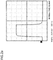
FIG. 2A is a chart showing an example of a relationship between time and an output of a red light emitting element; -
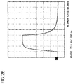
FIG. 2B is a chart showing an example of a relationship between time and an output of a green light emitting element; -
FIG. 2C is a chart showing an example of a relationship between time and an output of a blue light emitting element; -
FIG. 3 is a timing chart illustrating an example operation of acontrol unit 20 ofFIG. 1 ; -
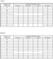
FIG. 4 is a chart illustrating in detail a control applied to green light emitting elements L21 - L24 ofFIG. 1 ; -
FIG. 5 is a chart illustrating in detail a control applied to red light emitting elements L11 - L14 ofFIG. 1 ; -
FIG. 6 is a timing chart illustrating another example operation of thecontrol unit 20 ofFIG. 1 ; -
FIG. 7 is a chromaticity diagram based on TABLE 1; and -
FIG. 8 is a chromaticity diagram based on TABLE 2. -
FIG. 1 is a circuit diagram of adisplay device 1 according to an embodiment of the present invention. As shown inFIG. 1 , thedisplay device 1 includes adisplay unit 10 and acontrol unit 20. Thedisplay unit 10 includes a plurality of light emitting elements L11 - L34 (i.e., L11, L12, L13, L14, L21, L22, L23, L24, L31, L32, L33, and L34),common lines COM 1 and COM2, a power supply V, and drive lines SEG11 - SEG32 (i.e., SEG 11, SEG 12, SEG 21, SEG 22, SEG 31, and SEG 32). The plurality of light emitting elements L11 - L34 configured with red light emitting elements L11 - L14, green light emitting elements L21 - L24, and blue light emitting elements L31 - L34. Each component will be explained in detail below. - The
display unit 10 has a plurality of pixels. Each pixel, for example, is structured with one or more of the red light emitting elements L11 - L14, one or more of the green light emitting elements L21- L24, and one or more of the blue light emitting elements L31- L34. The red light emitting elements L11 - L14 typically refer to those light emitting elements each having a peak emission wavelength range from 615 nm to 645 nm at a 20 mA of forward current. The green light emitting elements L21 - L24 typically refer to those light emitting elements each having a peak emission wavelength range from 500 nm to 560 nm at a 20 mA of forward current. The blue light emitting elements L31 - L34 typically refer to those light emitting elements each having a peak emission wavelength range from 450 nm to 490 nm at a 20 mA of forward current. For each light emitting element, a light emitting diode (LED), for example, can be used. -
FIG. 2A is a chart showing an example of a relationship between time and an output of one of the red light emitting elements.FIG. 2B is an example of a relationship between time and an output of one of the green light emitting elements.FIG. 2C is an example of a relationship between time and an output of one of the blue light emitting elements. InFIGS. 2A to 2C , the horizontal axis represents time, and the vertical axis represents output. InFIGS. 2A to 2C each division on the horizontal axis represents 200 ns. As shown inFIGS. 2A to 2C , when a light emitting element is pulse-driven, the output of the light emitting element is unstable when the output rises and falls. In the following explanations, the state in which the output of a light emitting element is stable will be referred to as a steady state, and the state in which the output of a light emitting element is unstable will be referred to as a transient state. A period during which a light emitting element is in a steady state will be referred to as a steady state period, and a period during which a light emitting element is in a transient state will be referred to as a transient state period. In the case of a very short steady state period, it is difficult to allow a light emitting element to turn on with a luminance close to the desired luminance or with a chromaticity close to the desired chromaticity. A lighting period (i.e., the period from the rise to the fall of the output of a light emitting element) constitutes a steady state period and transient state periods. - The output rise time of the red light emitting elements L11 - L14 is about 40 ns to about 45 ns, and the output fall time thereof is about 50 ns to 55 ns. The output rise time of the blue light emitting elements L31 - L34 is about 60 ns to about 70 ns, and the output fall time thereof is about 80 ns to about 100 ns. In contrast, the output rise time of the green light emitting elements L21- L24 is about 130 ns to 150 ns, and the output fall time thereof is about 220 ns to about 240 ns. As such, the green light emitting elements L21 - L24 have longer output rise time and longer output fall time as compared to the red light emitting elements L11 - L14 and the blue light emitting elements L31 - L34. For this reason, in the case of the green light emitting elements L21 - L24 whose lighting period is very short, the lighting period is dominantly accounted for by transient periods to thereby shorten the steady state period which makes it difficult to turn on the light emitting elements with a chromaticity close to the desired chromaticity.
- As compared to the red light emitting elements L11 - L14 and the blue light emitting elements L31 - L34, the green light emitting elements L21 - L24 tend to have more extensive chromaticity variance attributable to the variance of the current supplied. The details of the reason for this are unclear, but are believed to be attributable to the fact that LEDs are primarily used as the light emitting elements. In general, both blue and green LEDs are made of nitride semiconductors, but a green LED contains more indium in the active layer where light is emitted, which is believed to be the cause of the extensive chromaticity variance resulting from varying current values. Accordingly, compared to the red light emitting elements L11 - L14 and the blue light emitting elements L31 - L34, the green light emitting elements L21- L24 tend to have a chromaticity shift between a steady state period and a transient state period, and when the steady state period is very short, the chromaticity shift from what is desired tends to be extensive.
- The red light emitting elements L11 - L14 and the blue light emitting elements L31- L34 have relatively short output rise time and short output fall time compared to those of the green light emitting elements L21- L24. For this reason, even in the case of a very short lighting period, a relatively long steady state period can be ensured. Moreover, the red light emitting elements L11 - L14 and the blue light emitting elements L31- L34 have relatively small chromaticity variance attributable to current value variance, and the chromaticity does not shift much between a steady state period and a transient state period. Accordingly, it is relatively easy to turn on the red light emitting elements L11 - L14 and the blue light emitting elements L31 - L34 with a chromaticity close to the desired chromaticity.
- The common lines COM1 and COM2 are respectively connected to ends of the light emitting elements L11 - L34. The light emitting elements L11 - L34 may be connected to the common lines COM1 and COM2 at their common anode or common cathode. The common lines COM1 and COM2 may be branched or diverged along the way. In the present embodiment, two common lines are provided, but the number of common lines may be any as long as it is one or more.
- A plurality of drive lines SEG11 - SEG32 are connected to the respective other ends of the light emitting elements L11 - L34.
- Copper foil or the like can be used for the common lines COM1 and COM2, and the drive lines SEG11 - SEG32. Copper foil refers to the wiring provided on a printed wiring board. The common lines COM1 and COM2, and the drive lines SEG11 - SEG32 can be formed into various shapes on a printed wiring board, such as linear, planar (e.g., a square or circular shape), or the like. The use of the term, "line," is not intended to limit the actual shapes of the common lines COM1 and COM2, or the drive lines SEG11 - SEG32. The term is merely used to schematically describe the common lines COM1 and COM2, and the drive lines SEG11 - SEG32 in a circuit diagram.
- The power supply V supplies voltage to the light emitting elements L11 - L34. In the case where two or more common lines are provided, the power supply V may be provided per common line. However, the power supply V can be shared by two or more common lines. In the case where the power supply V is shared by two or more common lines, the voltage supplied by the power supply V may always be applied to each common line by way of static control, or may be applied by way of time-divided dynamic control. For example, a series or switched mode constant voltage direct current power supply can be used for the power supplies V.
- The source drivers SW11 and SW12 are switches for connecting the common lines COM1 and COM2 to the power supply V, and are turned ON or OFF by the
control unit 20 using a time-division switching technique. For the source drivers SW11 and SW12, a P-channel FET or PNP transistor can be used. FET stands for "field effect transistor". - The sink drivers SW21 - SW26 are respectively connected to the drive lines SEG11- SEG32. The sink drivers SW21 - SW26 are switches for connecting the drive lines SEG11 - SEG32 to GND, and are turned ON or OFF by the
control unit 20. For the sink drivers SW21 - SW26, an NPN transistor or N-channel FET can be used. The electric current flowing to the drive lines SEG11 - SEG32 can be controlled by an element or device, such as a resistor, constant current source, or the like. These elements or devices can be disposed between the individual sink drivers SW21 - SW26 and GND, or between the individual sink drivers SW21 - SW26 and the light emitting elements L11 - L34. - For the
control unit 20, an FPGA, microcomputer, or combination of these can be used. FPGA stands for "field programmable gate array". - The
control unit 20 controls individual light emitting elements L11 - L34. They are controlled by using, for example, pulse width modulation (PWM). In other words, thecontrol unit 20 controls the light emitting elements L11 - L34 by turning ON or OFF the sink drivers SW21 - SW26 to apply voltage having a predetermined pulse width to the light emitting elements L11 - L34. To give an example, thecontrol unit 20 supplies an electric current by turning ON or OFF the sink drivers SW12 and SW25 to apply voltage having a predetermined pulse width along the route: power supply V → common line COM2 → light emitting element L24 → drive line SEG22 → GND. This turns on the light emitting element L24 for a predetermined period of time. -
FIG. 3 is a timing chart explaining an example of the operation of thecontrol unit 20. As shown inFIG. 3 , thecontrol unit 20 controls individual light emitting elements L11 - L34 in each of the plurality of main frames. Each main frame includes a plurality of sub-frames, and thecontrol unit 20 applies voltage having a predetermined pulse width to the light emitting elements L11 - L34 in each of the individual sub-frames. The length of a main frame is preferably 16.7 ms (60 Hz) or 20 ms (50 Hz) if an image or the like is displayed using multiple main frames, and preferably from 8 ms to 15 ms, if a text message is displayed. - The pulse widths of the voltages in individual sub-frames correspond to the gradation values for the individual sub-frames. The higher the gradation value, the longer the pulse width becomes, and the lower the gradation value, the shorter the pulse width becomes. The quantitative relationship between pulse width and gradation value can be defined in various ways. In the present embodiment, "zero" gradation value corresponds to "zero" pulse width, i.e., when the gradation value is zero, the pulse width is zero. Even in the case of not turning on the light emitting elements, it might be occasionally described herein that "the light emitting elements are turned on at 0 gradation value," or "electric current is supplied to the light emitting elements by applying voltage having 0 pulse width."
- The gradation values for individual sub-frames are determined according to the gradation data externally input based on output from an external device. The gradation data includes at least one of the following: gradation values for individual main frames, gradation values for individual sub-frames, and the data from which these gradation values can be derived. The gradation value for one main frame equals the sum of the gradation values for the sub-frames constituting the main frame. The
control unit 20, the external device which outputs gradation data, or the like, distributes the gradation value of individual main frames to the plurality of sub-frames constituting the main frame. Thedisplay device 1 may include amemory 30 that stores the gradation value for each sub-frame. In this case, thecontrol unit 20 controls lighting of the light emitting elements L11 - L34 based on the gradation values stored in thememory 30. -
FIG. 4 is a chart that explains in detail how the green light emitting elements L21 - L24 are controlled. InFIG. 4 , the leftmost column shows the gradation values for a main frame, and four other columns on the right show the gradation values for the sub-frames that constitute the main frame. In the example shown inFIG. 3 , one main frame is structured with four sub-frames. - In the case where the gradation value of the main frame is 0 or 1, or 7 or higher, the
control unit 20 controls lighting of the green light emitting elements L21- L24 such that the difference between the gradation value of a sub-frame having the maximum gradation value and the gradation value of a sub-frame having the minimum gradation value is 1 at most. For example, when the gradation value of the main frame is 7, thesub-frames sub-frame 1 has the minimum gradation value. The gradation value of thesub-frame sub-frame 1 is 1, and thus the difference between the gradation value of a sub-frame having the maximum gradation value and the gradation value of a sub-frame having the minimum gradation value is 1. - In contrast, for the main frames each having the gradation value of 2 or higher but 6 at most, the
control unit 20 controls lighting of the green light emitting elements L21 - L24 such that the difference between the gradation value of a sub-frame having the maximum gradation value and the gradation value of a sub-frame having the minimum gradation value is at least 2. For example, for the main frame having the gradation value of 6, thesub-frames sub-frame 1 has the minimum gradation value. The gradation value of thesub-frame sub-frame 1 is 0, and thus the difference between the gradation value of sub-frames having the maximum gradation value and the gradation value of a sub-frame having the minimum gradation value is 2. -
FIG. 5 is a chart that explains in detail how the red light emitting elements L11 - L14 are controlled. Similar toFIG. 4 , the leftmost column shows the gradation values for a main frame, and the four other columns on the right show the gradation values for the sub-frames that constitute the main frame. In the example shown inFIG. 5 , one main frame is also structured with four sub-frames as shown inFIG. 4 . - The
control unit 20 controls lighting of the red light emitting elements L11 - L14 such that the difference between the gradation value of a sub-frame having the maximum gradation value and the gradation value of a sub-frame having the minimum gradation value is 1 at most, regardless of the gradation value of the main frame. For example, if the gradation value of the main frame is 6, thesub-frames sub-frames sub-frame sub-frame - The blue light emitting elements L31 - L34 are controlled in the same way as the red light emitting elements Lull - L14, and thus the drawing and the explanation for them will be omitted.
- As described above, the
control unit 20 controls lighting of the green light emitting elements L21 - L24 so that the difference between the gradation value of a sub-frame having the maximum gradation value and the gradation value of a sub-frame having the minimum gradation value is at least 2, if the gradation value of the main frame is at least 2 but 6 at most. In this manner, even if the gradation value of a main frame is too low to distribute adequately large graduation values to all sub-frames, in other words, where the desired chromaticity cannot be obtained in any sub-frame, the green light emitting elements L21 - L24 can be turned on in a sub-frame having the maximum gradation value using a relatively high gradation value. In addition, even though a chromaticity shift is likely to occur in a sub-frame having the minimum gradation value due to an increased transient state period as compared to the steady state period, the shift would not be distinguishable because the lighting period for the light emitting elements itself is shorter than that of the other sub-frames, or they are not turned on. Accordingly, the green light emitting elements L21- L24 can be turned on with a chromaticity that is close to the desired chromaticity when the green light emitting elements L21- L24 are viewed in a main frame as a whole. The gradation value of a sub-frame having the maximum gradation value is high, but the gradation value of the main frame as a whole can be maintained because the gradation value of a sub-frame having the minimum gradation value is kept low. - The
control unit 20 controls lighting of the red light emitting elements L11 - L14 and the blue light emitting elements L31 - L34 such that the difference between the gradation value of a sub-frame having the maximum gradation value and the gradation value of a sub-frame having the minimum gradation value is 1 at most, regardless of the gradation value of the main frame. This reduces the time where the light emitting elements are continuously not turned on, thereby reducing the occurrences of a flickering phenomenon, i.e., wavering of a displayed image. The red light emitting elements L11 - L14 and the blue light emitting elements L31 - L34 have a larger steady state period in the total lighting period even when having a short lighting period as compared to the green light emitting elements L21 - L24. For this reason, they can relatively be easy to obtain a chromaticity close to the desired chromaticity even if the lighting is controlled as described above. - According to the present embodiment discussed above, a display device can be provided in which the difference between a desired chromaticity and the chromaticity actually obtained is less likely to be distinguishable even when the luminance is relatively low.
- The pulse width in a sub-frame having the maximum gradation value is preferably longer than 100 ns, more preferably longer than 200 ns. This can increase the steady state period even for the green light emitting elements L21 - L24, thereby allowing them to turn on with a chromaticity that is close to the desired chromaticity.
- The steady state period with respect to a total lighting period in a sub-frame having the maximum gradation value is preferably at least 50%. This allows the green light emitting elements L21- L24 to turn on with a chromaticity that is even closer to the desired chromaticity in a sub-frame having the maximum gradation value. The steady state period with respect to a total lighting period in a sub-frame having the minimum gradation value is preferably 50% at most. This makes the lighting period for the light emitting elements itself shorter in a sub-frame having the minimum gradation value than that in the other sub-frames, or they are not turned on, thereby allowing the green light emitting elements L21 - L24 to turn on with a chromaticity that is even closer to the desired chromaticity in a sub-frame having the minimum gradation value when viewed in a main frame as a whole.
- In the present embodiment, as predetermined light emitting elements, the green light emitting elements L21 - L24, are controlled differently from the red light emitting elements L11 - L14 and the blue light emitting elements L31 - L34. However, all light emitting elements may be, as predetermined light emitting elements, controlled to turn on such that the difference between the gradation value of a sub-frame having the maximum gradation value and the gradation value of a sub-frame having the minimum gradation value is at least 2. This can unify the lighting control method thereby simplifying the method for controlling the light emitting elements.
- In the present embodiment, the green light emitting elements L21- L24 are controlled such that the difference between the gradation value of a sub-frame having the maximum gradation value and the gradation value of a sub-frame having the minimum gradation value is at least 2 for a predetermined main frame having a gradation value of 2 or higher but 6 or lower. However, the main frame in which this control method is applied can be suitably determined. Alternatively, this control method can be applied to all main frames. The present embodiment is particularly effective in the case where the gradation value of at least one of the sub-frames cannot turn on the subject light emitting elements with a desired chromaticity, assuming that the gradation value of one main frame is equally distributed among multiple sub-frames that constitute the main frame. If equal distribution is impossible, the gradation value can be distributed to the sub-frames in such a way that the difference between the gradation value of a sub-frame having the maximum gradation value and the gradation value of a sub-frame having the minimum gradation value is 1 at most, in order to obtain the above-mentioned effect.
-
FIG. 6 is a timing chart explaining another example of the operation of thecontrol unit 20. As shown inFIG. 6 , thecontrol unit 20, in the case where a predetermined main frame includes a plurality of sub-frames having the maximum gradation value and a plurality of sub-frames having the minimum gradation value, preferably turns on predetermined light emitting elements such that the sub-frames having the maximum gradation values and the sub-frames having the minimum gradation values alternate. In other words, the control unit preferably applies control, if the gradation value of the main frame is 4, for example, such that the gradation value of thesub-frames sub-frames sub-frames sub-frame - The display device in an example will be explained next.
- The display device in the Example includes 1728 light emitting elements arranged at 4 mm intervals both vertically and horizontally, 24 common lines arranged in a horizontal direction, 216 drive lines (72 × 3 colors) arranged in a vertical direction, a 5V DC constant voltage source as a power supply, an FPGA as a control unit, P-channel FETs as source drivers, and constant current driven NPN transistors as sink drivers.
- The display device has 576 pixels, each pixel including a red light emitting element, a green light emitting element, and a blue light emitting element. In other words, the 1728 light emitting elements consist of 576 red light emitting elements, 576 green light emitting elements, and 576 blue light emitting elements. The sink drivers are set to supply a 16.8 mA current to the red light emitting elements, 18.7 mA current to the green light emitting elements, and 16.8 mA current to the blue light emitting elements. The common lines are respectively connected to the anode sides of the light emitting elements, and the drive lines are respectively connected to the cathode sides of the light emitting elements.
- Voltage is applied to each common line using a time-division dynamic lighting system. The duty ratio is 1/24, and the duration of voltage application per common line is 47.9 µs, and the duration when no voltage is applied to any common line is 10 µs. Here (47.9 µs + 10 µs) × 24 duty = 1.389 ms. Thus, the length of a sub-frame is 1.389 ms.
- A main frame is configured with 32 sub-frames. 1.389 ms × 32 = 44.4 ms, and thus the length of a main frame is 44.4 ms.
- The gradation value for each sub-frame is set to be controlled by pulse width modulation to 64 levels (0 - 63). The gradation value for the entire main frame can be controlled to 2048 levels (0 - 2047; 32 sub-frames × 64 levels).
Pulse width and gradation value are assumed to be in the relationship: Pulse Width = Gradation Value × 72.9 ns. - It is assumed that the green light emitting elements can achieve a chromaticity close to the desired chromaticity (i.e., the chromaticity achieved when the pulse width is adequately large; hereinafter the same applies in the Example) by applying voltage having a pulse width of at least 1166.7 ns, in other words, voltage of a gradation value of at least 16 (i.e., 1166.7 ns/72.9 ns ≈ 16). On the other hand, it is assumed that the red and blue light emitting elements can achieve a chromaticity close to the desired chromaticity by applying voltage having a pulse width of at least 72.9 ns, in other words, voltage of a gradation value of at least 1 (i.e., 72.9 ns/72.9 ns = 1).
- The cases where the gradation values for the green light emitting elements in a main frame in the display device described above are 1024 and 32 will be examined.
- When the gradation value of a main frame is 1024, the main frame is set such that the total gradation value 1024 is equally distributed among the sub-frames, and the green light emitting elements are turned on in each sub-frame using a gradation value of 32 (the gradation value of the entire main frame 1024 / the number of sub-frames 32 = 32). Accordingly, the pulse width in each sub-frame is 2333.3 ns (i.e., 72.9 ns × gradation value 32 = 2333.3 ns), and the green light emitting elements turn on with desired chromaticity.
- In the case where the gradation value 32 of an entire main frame is equally distributed among the sub-frames, the gradation value for each sub-frame would be 1 (i.e., the gradation value of the entire main frame 32 / the number of sub-frames 32 = 1). The pulse width for each sub-frame would thus be 72.9 ns (72.9 ns ×
gradation value 1 = 72.9 ns), making the chromaticity of the green light emitting elements unstable to achieve the desired chromaticity in all sub-frames. Accordingly, in the case where the gradation value for the entire main frame is 32, the control unit is set to turn on the green light emitting elements such that the sub-frames having a gradation value of 0 (i.e., gradation value not resulting in a desired chromaticity) and the sub-frames having a gradation value of 2 (gradation value achieving a chromaticity close to the desired chromaticity) alternate. - The control unit is set to control to turn on the red and blue light emitting elements using a gradation value of 1 in all sub-frames whether the gradation value for the green light emitting elements in a main frame is 1024 or 32.
- TABLE 1 shows the chromaticity obtained by the lighting control method described above, and
FIG. 7 shows the chromaticity diagram based on TABLE 1.TABLE 1 Gradation Value White Red Green Blue x y x y x y x y 32 0.290 0.334 0.696 0.303 0.241 0.708 0.137 0.055 1024 0.290 0.301 0.696 0.303 0.209 0.720 0.139 0.050 - Here, in TABLE 1, the "Red" columns show the chromaticity obtained by the red light emitting elements, the "Green" columns show the chromaticity obtained by the green light emitting elements, the "Blue" columns show the chromaticity obtained by the blue light emitting elements, and the "White" columns show the chromaticity obtained by all of the red light emitting elements, green light emitting elements, and blue light emitting elements. In other words, the "White" columns show the composite chromaticity that combines the chromaticity obtained by the red, green, and blue light emitting elements.
- As shown in TABLE 1, in the display device in this Example, when the gradation value for the entire main frame is 32, the values x and y of the green light emitting elements are respectively 0.241 and 0.708. Also, when the gradation value of the entire main frame is 1024, the values x and y of the green light emitting elements are respectively 0.209 and 0.720. Accordingly, for the green light emitting elements, there is a shift of 0.032 (= 0.241 - 0.209) in x value and a shift of 0.012 (= 0.720 - 0.708) in y value between the total main frame gradation values of 32 and 1024. When the gradation value is 32, the luminance of the light emitting elements is 7.2 cd/m2 for "White", 1.3 cd/m2 for "Red", 5.2 cd/m2 for "Green", and 0.5 cd/m2 for "Blue". When the gradation value is 1024, the luminance of the light emitting elements is 206.5 cd/m2 for "White", 48.8 cd/m2 for "Red", 141.0 cd/m2 for "Green", and 16.4 cd/m2 for "Blue".
- A display device in a Comparative Example will be explained next.
- The display device in the Comparative Example differs from the display device in the Example in terms of the lighting control method for the green light emitting elements. It is otherwise the same as or similar to the display device in the Example. To specifically explain, in the Comparative Example, even when the gradation value for the entire main frame is 32, the gradation value for the entire main frame is equally distributed to the sub-frames, and the green light emitting elements are turned on with a gradation value of 1 (i.e., the gradation value resulting in unstable chromaticity) in all sub-frames. TABLE 2 shows the chromaticity obtained by such lighting control, and
FIG. 8 shows the chromaticity diagram based on TABLE 2.TABLE 2 Gradation Value White Red Green Blue x y x y x y x y 32 0.294 0.357 0.696 0.303 0.263 0.699 0.137 0.055 1024 0.289 0.300 0.696 0.303 0.208 0.721 0.139 0.050 - As shown in TABLE 2, in the display device in the Comparative Example, when the gradation value for the entire main frame is 32, the values x and y of the green light emitting elements are respectively 0.263 and 0.699. Also, when the gradation value is 1024, the values x and y of the green light emitting elements are respectively 0.208 and 0.721. Accordingly, for the green light emitting elements, there is a shift of 0.055 (= 0.263 - 0.208) in x value, and a shift of 0.022 (= 0.721 - 0.699) in y value between the total main frame gradation values of 32 and 1024. When the gradation value is 32, the luminance of the light emitting elements is 8.0 cd/m2 for "White", 1.3 cd/m2 for "Red", 5.9 cd/m2 for "Green", and 0.5 cd/m2 for "Blue". When the gradation value is 1024, the luminance of the light emitting elements is 204.9 cd/m2 for "White", 48.5 cd/m2 for "Red", 140.9 cd/m2 for "Green", and 16.4 cd/m2 for "Blue".
- As discussed above, in the display device in the Comparative Example, there is an x value shift of 0.055 and a y value shift of 0.022 for the green light emitting elements between the total main frame gradation values of 32 and 1024. In contrast, according to the display device in the Example, the x value shift can be reduced to 0.032, and the y value shift can be reduced to 0.012. Accordingly, the display device of the Example can bring the chromaticity of the green light emitting elements closer to the desired chromaticity under the condition that the total gradation value of a main frame is low, compared to the display device in the Comparative Example.
- The certain embodiment and example explained above merely illustrate examples, and do not in any way limit the present invention as defined by the scope of the claims.
- The display device according to the present invention can be utilized, for example, in a large screen television as well as a message board displaying information such as traffic updates.
Claims (7)
- A display device comprising:a display unit including a plurality of light emitting elements: anda control unit that individually controls the plurality of light emitting elements in each of a plurality of main frames according to gradation data externally input based on output from an external device, whereinthe plurality of main frames each include a plurality of sub-frames, andthe control unit turns on predetermined ones of the plurality of light emitting elements in a predetermined one of the plurality of main frames such that a difference between a gradation value of one or more of the plurality of sub-frames having a maximum gradation value and a gradation value of one or more of the plurality of sub-frames having a minimum gradation value is at least 2.
- The display device according to claim 1 further comprising:a memory for storing the gradation values to be distributed to the plurality of sub-frames that constitute one of the plurality of main frames,
whereinthe control unit individually turns on the plurality of light emitting elements based on the gradation values stored in the memory. - The display device according to any of the preceding claims, wherein
the control unit, in the predetermined one of the plurality of main frames, turns on the predetermined ones of the plurality of light emitting elements such that a steady state period with respect to a total lighting period in the one or more sub-frames having the maximum gradation value is at least 50%, while turning on the predetermined ones of the plurality of light emitting elements such that the steady state period with respect to the total lighting period in the one or more sub-frames having the minimum gradation value is 50% at most. - The display device according to any of the preceding claims, wherein
the predetermined one of the plurality of main frames constitute the one or more sub-frames having the maximum gradation value, and the one or more sub-frame having the minimum gradation value, and
the control unit, in the predetermined one of the plurality of main frames, turns on the predetermined ones of the plurality of light emitting elements such that the one or more sub-frames having the maximum gradation value and the one or more sub-frames having the minimum gradation values alternate. - The display device according to any of the preceding claims, wherein
the control unit applies voltage to the plurality of light emitting elements by pulse width modulation, and
the pulse width in the one or more sub-frames having the maximum gradation value is longer than 100 ns. - The display device according to any of the preceding claims, wherein
the plurality of light emitting elements include one or more green light emitting elements. - The display device according to any of the preceding claims, wherein
the display unit includes a plurality of pixels,
the plurality of pixels each include at least one red light emitting element, at least one green light emitting element, and at least one blue light emitting element, and
the predetermined ones of the plurality of light emitting elements include one or more green light emitting elements.
Applications Claiming Priority (1)
| Application Number | Priority Date | Filing Date | Title |
|---|---|---|---|
| JP2016230744A JP6774320B2 (en) | 2016-11-29 | 2016-11-29 | Display device |
Publications (2)
| Publication Number | Publication Date |
|---|---|
| EP3327708A1 true EP3327708A1 (en) | 2018-05-30 |
| EP3327708B1 EP3327708B1 (en) | 2021-04-28 |
Family
ID=60452523
Family Applications (1)
| Application Number | Title | Priority Date | Filing Date |
|---|---|---|---|
| EP17203526.3A Active EP3327708B1 (en) | 2016-11-29 | 2017-11-24 | Display device |
Country Status (3)
| Country | Link |
|---|---|
| US (1) | US10475373B2 (en) |
| EP (1) | EP3327708B1 (en) |
| JP (1) | JP6774320B2 (en) |
Families Citing this family (4)
| Publication number | Priority date | Publication date | Assignee | Title |
|---|---|---|---|---|
| JP6774320B2 (en) * | 2016-11-29 | 2020-10-21 | 日亜化学工業株式会社 | Display device |
| JP6673300B2 (en) * | 2017-06-28 | 2020-03-25 | 日亜化学工業株式会社 | Display device |
| JP2020177121A (en) * | 2019-04-18 | 2020-10-29 | 日亜化学工業株式会社 | Display device and its manufacturing method |
| CN113327540A (en) * | 2021-06-01 | 2021-08-31 | 成都辰显光电有限公司 | Display panel, driving method thereof and display device |
Citations (4)
| Publication number | Priority date | Publication date | Assignee | Title |
|---|---|---|---|---|
| US20060232601A1 (en) * | 2005-04-14 | 2006-10-19 | Semiconductor Energy Laboratory Co., Ltd. | Display device, and driving method and electronic apparatus of the display device |
| JP2010054989A (en) | 2008-08-29 | 2010-03-11 | Mitsubishi Electric Corp | Gradation control method and display device |
| JP2013019921A (en) * | 2009-11-10 | 2013-01-31 | Panasonic Corp | Liquid crystal display device |
| US20160321980A1 (en) * | 2015-04-30 | 2016-11-03 | Nichia Corporation | Display apparatus, lighting control circuit, and method of lighting display apparatus |
Family Cites Families (18)
| Publication number | Priority date | Publication date | Assignee | Title |
|---|---|---|---|---|
| JP3161548B2 (en) * | 1991-11-05 | 2001-04-25 | 日本放送協会 | Halftone image display method and halftone image display device |
| JP3598664B2 (en) * | 1996-07-22 | 2004-12-08 | 株式会社デンソー | EL display device |
| JPH10149128A (en) * | 1996-11-18 | 1998-06-02 | Mk Seiko Co Ltd | Display device |
| JP2000148088A (en) * | 1998-11-16 | 2000-05-26 | Tdk Corp | Drive assembly for organic el display device |
| JP2003099003A (en) | 2000-02-03 | 2003-04-04 | Nichia Chem Ind Ltd | Image display device, image display control method, and image display device control method |
| JP3368890B2 (en) | 2000-02-03 | 2003-01-20 | 日亜化学工業株式会社 | Image display device and control method thereof |
| JP3720322B2 (en) | 2002-11-26 | 2005-11-24 | 名古屋電機工業株式会社 | Display method for outdoor display device, outdoor display device, and display control program |
| JP4341839B2 (en) * | 2003-11-17 | 2009-10-14 | シャープ株式会社 | Image display device, electronic apparatus, liquid crystal television device, liquid crystal monitor device, image display method, display control program, and recording medium |
| JP4327676B2 (en) * | 2004-07-28 | 2009-09-09 | 株式会社東芝 | Image printing method and image printing apparatus |
| JP2006119212A (en) | 2004-10-19 | 2006-05-11 | Mitsubishi Electric Corp | Electronics |
| JP2006195306A (en) * | 2005-01-17 | 2006-07-27 | Sony Corp | LIGHT EMITTING DEVICE DRIVE METHOD, LIGHT EMITTING DEVICE DRIVE DEVICE, AND DISPLAY DEVICE |
| US8130246B2 (en) * | 2005-03-14 | 2012-03-06 | Sharp Kabushiki Kaisha | Image display apparatus, image display monitor and television receiver |
| JP4954579B2 (en) * | 2005-04-14 | 2012-06-20 | 株式会社半導体エネルギー研究所 | Driving method of display device |
| JP5278730B2 (en) * | 2008-04-16 | 2013-09-04 | Nltテクノロジー株式会社 | CONTROLLER, HOLD TYPE DISPLAY, ELECTRONIC DEVICE, SIGNAL ADJUSTMENT METHOD FOR HOLD TYPE DISPLAY |
| JP5733154B2 (en) * | 2011-10-27 | 2015-06-10 | 株式会社Jvcケンウッド | Liquid crystal display |
| JP6255709B2 (en) * | 2013-04-26 | 2018-01-10 | 株式会社Jvcケンウッド | Liquid crystal display |
| JP6774320B2 (en) * | 2016-11-29 | 2020-10-21 | 日亜化学工業株式会社 | Display device |
| JP6520907B2 (en) * | 2016-12-21 | 2019-05-29 | 日亜化学工業株式会社 | Display device |
-
2016
- 2016-11-29 JP JP2016230744A patent/JP6774320B2/en active Active
-
2017
- 2017-11-24 EP EP17203526.3A patent/EP3327708B1/en active Active
- 2017-11-27 US US15/822,208 patent/US10475373B2/en active Active
Patent Citations (4)
| Publication number | Priority date | Publication date | Assignee | Title |
|---|---|---|---|---|
| US20060232601A1 (en) * | 2005-04-14 | 2006-10-19 | Semiconductor Energy Laboratory Co., Ltd. | Display device, and driving method and electronic apparatus of the display device |
| JP2010054989A (en) | 2008-08-29 | 2010-03-11 | Mitsubishi Electric Corp | Gradation control method and display device |
| JP2013019921A (en) * | 2009-11-10 | 2013-01-31 | Panasonic Corp | Liquid crystal display device |
| US20160321980A1 (en) * | 2015-04-30 | 2016-11-03 | Nichia Corporation | Display apparatus, lighting control circuit, and method of lighting display apparatus |
Also Published As
| Publication number | Publication date |
|---|---|
| JP2018087887A (en) | 2018-06-07 |
| US20180151110A1 (en) | 2018-05-31 |
| US10475373B2 (en) | 2019-11-12 |
| EP3327708B1 (en) | 2021-04-28 |
| JP6774320B2 (en) | 2020-10-21 |
Similar Documents
| Publication | Publication Date | Title |
|---|---|---|
| CN110718195B (en) | Light emitting device, display device, and LED display device | |
| JP4295163B2 (en) | Display device, organic electroluminescent display device, and display device driving method | |
| US10546530B2 (en) | Pixel driving circuit and display device thereof | |
| KR100686334B1 (en) | Display device and driving method thereof | |
| US7315292B2 (en) | Electric current adjustment of light emitting element of display device | |
| KR102738532B1 (en) | Led driver and led driving method | |
| US20050116656A1 (en) | Amoled display and driving method thereof | |
| EP3327708B1 (en) | Display device | |
| KR20050046469A (en) | Pixel circuit in display device and driving method thereof | |
| US9622307B2 (en) | Apparatus and technique for modular electronic display control | |
| US20210217348A1 (en) | Display device and light-emitting control circuit thereof, driving method | |
| WO2010007808A1 (en) | Light emitting element driving circuit | |
| US12555525B2 (en) | Driver circuit for light emitting modules with combined active and passive matrix functionalities | |
| EP1568004A1 (en) | Colour control for active matrix electroluminescent display | |
| JP7101463B2 (en) | Light emitting element drive device, semiconductor device, light emitting device and liquid crystal display device | |
| US10467945B2 (en) | Display device | |
| US12230203B2 (en) | Display apparatus | |
| CN111316345A (en) | Sub-pixel circuit, active type electroluminescent display and driving method thereof | |
| CN115035837A (en) | Light board and control method thereof, and display panel | |
| KR100632808B1 (en) | Active matrix display panel and device with simplified driving circuit | |
| JP6442885B2 (en) | Display device | |
| KR101266395B1 (en) | Driving method of display device and device appling the same | |
| KR20020074567A (en) | apparatus for power supply in indicating element | |
| KR20060095132A (en) | Organic electroluminescent display | |
| JP2006072227A (en) | Drive circuit of display device |
Legal Events
| Date | Code | Title | Description |
|---|---|---|---|
| PUAI | Public reference made under article 153(3) epc to a published international application that has entered the european phase |
Free format text: ORIGINAL CODE: 0009012 |
|
| STAA | Information on the status of an ep patent application or granted ep patent |
Free format text: STATUS: THE APPLICATION HAS BEEN PUBLISHED |
|
| AK | Designated contracting states |
Kind code of ref document: A1 Designated state(s): AL AT BE BG CH CY CZ DE DK EE ES FI FR GB GR HR HU IE IS IT LI LT LU LV MC MK MT NL NO PL PT RO RS SE SI SK SM TR |
|
| AX | Request for extension of the european patent |
Extension state: BA ME |
|
| STAA | Information on the status of an ep patent application or granted ep patent |
Free format text: STATUS: REQUEST FOR EXAMINATION WAS MADE |
|
| 17P | Request for examination filed |
Effective date: 20181115 |
|
| RBV | Designated contracting states (corrected) |
Designated state(s): AL AT BE BG CH CY CZ DE DK EE ES FI FR GB GR HR HU IE IS IT LI LT LU LV MC MK MT NL NO PL PT RO RS SE SI SK SM TR |
|
| STAA | Information on the status of an ep patent application or granted ep patent |
Free format text: STATUS: EXAMINATION IS IN PROGRESS |
|
| 17Q | First examination report despatched |
Effective date: 20190513 |
|
| GRAP | Despatch of communication of intention to grant a patent |
Free format text: ORIGINAL CODE: EPIDOSNIGR1 |
|
| STAA | Information on the status of an ep patent application or granted ep patent |
Free format text: STATUS: GRANT OF PATENT IS INTENDED |
|
| INTG | Intention to grant announced |
Effective date: 20201119 |
|
| GRAS | Grant fee paid |
Free format text: ORIGINAL CODE: EPIDOSNIGR3 |
|
| GRAA | (expected) grant |
Free format text: ORIGINAL CODE: 0009210 |
|
| STAA | Information on the status of an ep patent application or granted ep patent |
Free format text: STATUS: THE PATENT HAS BEEN GRANTED |
|
| AK | Designated contracting states |
Kind code of ref document: B1 Designated state(s): AL AT BE BG CH CY CZ DE DK EE ES FI FR GB GR HR HU IE IS IT LI LT LU LV MC MK MT NL NO PL PT RO RS SE SI SK SM TR |
|
| REG | Reference to a national code |
Ref country code: GB Ref legal event code: FG4D |
|
| REG | Reference to a national code |
Ref country code: CH Ref legal event code: EP |
|
| REG | Reference to a national code |
Ref country code: AT Ref legal event code: REF Ref document number: 1387989 Country of ref document: AT Kind code of ref document: T Effective date: 20210515 |
|
| REG | Reference to a national code |
Ref country code: DE Ref legal event code: R096 Ref document number: 602017037502 Country of ref document: DE |
|
| REG | Reference to a national code |
Ref country code: IE Ref legal event code: FG4D |
|
| REG | Reference to a national code |
Ref country code: LT Ref legal event code: MG9D |
|
| REG | Reference to a national code |
Ref country code: AT Ref legal event code: MK05 Ref document number: 1387989 Country of ref document: AT Kind code of ref document: T Effective date: 20210428 |
|
| PG25 | Lapsed in a contracting state [announced via postgrant information from national office to epo] |
Ref country code: LT Free format text: LAPSE BECAUSE OF FAILURE TO SUBMIT A TRANSLATION OF THE DESCRIPTION OR TO PAY THE FEE WITHIN THE PRESCRIBED TIME-LIMIT Effective date: 20210428 Ref country code: FI Free format text: LAPSE BECAUSE OF FAILURE TO SUBMIT A TRANSLATION OF THE DESCRIPTION OR TO PAY THE FEE WITHIN THE PRESCRIBED TIME-LIMIT Effective date: 20210428 Ref country code: NL Free format text: LAPSE BECAUSE OF FAILURE TO SUBMIT A TRANSLATION OF THE DESCRIPTION OR TO PAY THE FEE WITHIN THE PRESCRIBED TIME-LIMIT Effective date: 20210428 Ref country code: AT Free format text: LAPSE BECAUSE OF FAILURE TO SUBMIT A TRANSLATION OF THE DESCRIPTION OR TO PAY THE FEE WITHIN THE PRESCRIBED TIME-LIMIT Effective date: 20210428 Ref country code: BG Free format text: LAPSE BECAUSE OF FAILURE TO SUBMIT A TRANSLATION OF THE DESCRIPTION OR TO PAY THE FEE WITHIN THE PRESCRIBED TIME-LIMIT Effective date: 20210728 Ref country code: HR Free format text: LAPSE BECAUSE OF FAILURE TO SUBMIT A TRANSLATION OF THE DESCRIPTION OR TO PAY THE FEE WITHIN THE PRESCRIBED TIME-LIMIT Effective date: 20210428 |
|
| PG25 | Lapsed in a contracting state [announced via postgrant information from national office to epo] |
Ref country code: IS Free format text: LAPSE BECAUSE OF FAILURE TO SUBMIT A TRANSLATION OF THE DESCRIPTION OR TO PAY THE FEE WITHIN THE PRESCRIBED TIME-LIMIT Effective date: 20210828 Ref country code: LV Free format text: LAPSE BECAUSE OF FAILURE TO SUBMIT A TRANSLATION OF THE DESCRIPTION OR TO PAY THE FEE WITHIN THE PRESCRIBED TIME-LIMIT Effective date: 20210428 Ref country code: GR Free format text: LAPSE BECAUSE OF FAILURE TO SUBMIT A TRANSLATION OF THE DESCRIPTION OR TO PAY THE FEE WITHIN THE PRESCRIBED TIME-LIMIT Effective date: 20210729 Ref country code: NO Free format text: LAPSE BECAUSE OF FAILURE TO SUBMIT A TRANSLATION OF THE DESCRIPTION OR TO PAY THE FEE WITHIN THE PRESCRIBED TIME-LIMIT Effective date: 20210728 Ref country code: PT Free format text: LAPSE BECAUSE OF FAILURE TO SUBMIT A TRANSLATION OF THE DESCRIPTION OR TO PAY THE FEE WITHIN THE PRESCRIBED TIME-LIMIT Effective date: 20210830 Ref country code: PL Free format text: LAPSE BECAUSE OF FAILURE TO SUBMIT A TRANSLATION OF THE DESCRIPTION OR TO PAY THE FEE WITHIN THE PRESCRIBED TIME-LIMIT Effective date: 20210428 Ref country code: RS Free format text: LAPSE BECAUSE OF FAILURE TO SUBMIT A TRANSLATION OF THE DESCRIPTION OR TO PAY THE FEE WITHIN THE PRESCRIBED TIME-LIMIT Effective date: 20210428 Ref country code: SE Free format text: LAPSE BECAUSE OF FAILURE TO SUBMIT A TRANSLATION OF THE DESCRIPTION OR TO PAY THE FEE WITHIN THE PRESCRIBED TIME-LIMIT Effective date: 20210428 |
|
| REG | Reference to a national code |
Ref country code: NL Ref legal event code: MP Effective date: 20210428 |
|
| PG25 | Lapsed in a contracting state [announced via postgrant information from national office to epo] |
Ref country code: ES Free format text: LAPSE BECAUSE OF FAILURE TO SUBMIT A TRANSLATION OF THE DESCRIPTION OR TO PAY THE FEE WITHIN THE PRESCRIBED TIME-LIMIT Effective date: 20210428 Ref country code: RO Free format text: LAPSE BECAUSE OF FAILURE TO SUBMIT A TRANSLATION OF THE DESCRIPTION OR TO PAY THE FEE WITHIN THE PRESCRIBED TIME-LIMIT Effective date: 20210428 Ref country code: CZ Free format text: LAPSE BECAUSE OF FAILURE TO SUBMIT A TRANSLATION OF THE DESCRIPTION OR TO PAY THE FEE WITHIN THE PRESCRIBED TIME-LIMIT Effective date: 20210428 Ref country code: DK Free format text: LAPSE BECAUSE OF FAILURE TO SUBMIT A TRANSLATION OF THE DESCRIPTION OR TO PAY THE FEE WITHIN THE PRESCRIBED TIME-LIMIT Effective date: 20210428 Ref country code: EE Free format text: LAPSE BECAUSE OF FAILURE TO SUBMIT A TRANSLATION OF THE DESCRIPTION OR TO PAY THE FEE WITHIN THE PRESCRIBED TIME-LIMIT Effective date: 20210428 Ref country code: SM Free format text: LAPSE BECAUSE OF FAILURE TO SUBMIT A TRANSLATION OF THE DESCRIPTION OR TO PAY THE FEE WITHIN THE PRESCRIBED TIME-LIMIT Effective date: 20210428 Ref country code: SK Free format text: LAPSE BECAUSE OF FAILURE TO SUBMIT A TRANSLATION OF THE DESCRIPTION OR TO PAY THE FEE WITHIN THE PRESCRIBED TIME-LIMIT Effective date: 20210428 |
|
| REG | Reference to a national code |
Ref country code: DE Ref legal event code: R097 Ref document number: 602017037502 Country of ref document: DE |
|
| PLBE | No opposition filed within time limit |
Free format text: ORIGINAL CODE: 0009261 |
|
| STAA | Information on the status of an ep patent application or granted ep patent |
Free format text: STATUS: NO OPPOSITION FILED WITHIN TIME LIMIT |
|
| 26N | No opposition filed |
Effective date: 20220131 |
|
| PG25 | Lapsed in a contracting state [announced via postgrant information from national office to epo] |
Ref country code: IS Free format text: LAPSE BECAUSE OF FAILURE TO SUBMIT A TRANSLATION OF THE DESCRIPTION OR TO PAY THE FEE WITHIN THE PRESCRIBED TIME-LIMIT Effective date: 20210828 Ref country code: AL Free format text: LAPSE BECAUSE OF FAILURE TO SUBMIT A TRANSLATION OF THE DESCRIPTION OR TO PAY THE FEE WITHIN THE PRESCRIBED TIME-LIMIT Effective date: 20210428 |
|
| PG25 | Lapsed in a contracting state [announced via postgrant information from national office to epo] |
Ref country code: MC Free format text: LAPSE BECAUSE OF FAILURE TO SUBMIT A TRANSLATION OF THE DESCRIPTION OR TO PAY THE FEE WITHIN THE PRESCRIBED TIME-LIMIT Effective date: 20210428 |
|
| REG | Reference to a national code |
Ref country code: CH Ref legal event code: PL |
|
| PG25 | Lapsed in a contracting state [announced via postgrant information from national office to epo] |
Ref country code: LU Free format text: LAPSE BECAUSE OF NON-PAYMENT OF DUE FEES Effective date: 20211124 Ref country code: IT Free format text: LAPSE BECAUSE OF FAILURE TO SUBMIT A TRANSLATION OF THE DESCRIPTION OR TO PAY THE FEE WITHIN THE PRESCRIBED TIME-LIMIT Effective date: 20210428 Ref country code: BE Free format text: LAPSE BECAUSE OF NON-PAYMENT OF DUE FEES Effective date: 20211130 |
|
| REG | Reference to a national code |
Ref country code: BE Ref legal event code: MM Effective date: 20211130 |
|
| PG25 | Lapsed in a contracting state [announced via postgrant information from national office to epo] |
Ref country code: LI Free format text: LAPSE BECAUSE OF NON-PAYMENT OF DUE FEES Effective date: 20211130 Ref country code: CH Free format text: LAPSE BECAUSE OF NON-PAYMENT OF DUE FEES Effective date: 20211130 |
|
| PG25 | Lapsed in a contracting state [announced via postgrant information from national office to epo] |
Ref country code: IE Free format text: LAPSE BECAUSE OF NON-PAYMENT OF DUE FEES Effective date: 20211124 |
|
| PG25 | Lapsed in a contracting state [announced via postgrant information from national office to epo] |
Ref country code: HU Free format text: LAPSE BECAUSE OF FAILURE TO SUBMIT A TRANSLATION OF THE DESCRIPTION OR TO PAY THE FEE WITHIN THE PRESCRIBED TIME-LIMIT; INVALID AB INITIO Effective date: 20171124 |
|
| P01 | Opt-out of the competence of the unified patent court (upc) registered |
Effective date: 20230522 |
|
| PG25 | Lapsed in a contracting state [announced via postgrant information from national office to epo] |
Ref country code: CY Free format text: LAPSE BECAUSE OF FAILURE TO SUBMIT A TRANSLATION OF THE DESCRIPTION OR TO PAY THE FEE WITHIN THE PRESCRIBED TIME-LIMIT Effective date: 20210428 |
|
| PG25 | Lapsed in a contracting state [announced via postgrant information from national office to epo] |
Ref country code: MK Free format text: LAPSE BECAUSE OF FAILURE TO SUBMIT A TRANSLATION OF THE DESCRIPTION OR TO PAY THE FEE WITHIN THE PRESCRIBED TIME-LIMIT Effective date: 20210428 |
|
| PG25 | Lapsed in a contracting state [announced via postgrant information from national office to epo] |
Ref country code: TR Free format text: LAPSE BECAUSE OF FAILURE TO SUBMIT A TRANSLATION OF THE DESCRIPTION OR TO PAY THE FEE WITHIN THE PRESCRIBED TIME-LIMIT Effective date: 20210428 |
|
| PG25 | Lapsed in a contracting state [announced via postgrant information from national office to epo] |
Ref country code: MT Free format text: LAPSE BECAUSE OF FAILURE TO SUBMIT A TRANSLATION OF THE DESCRIPTION OR TO PAY THE FEE WITHIN THE PRESCRIBED TIME-LIMIT Effective date: 20210428 |
|
| PGFP | Annual fee paid to national office [announced via postgrant information from national office to epo] |
Ref country code: FR Payment date: 20250930 Year of fee payment: 9 |
|
| PGFP | Annual fee paid to national office [announced via postgrant information from national office to epo] |
Ref country code: DE Payment date: 20250930 Year of fee payment: 9 |
|
| PGFP | Annual fee paid to national office [announced via postgrant information from national office to epo] |
Ref country code: GB Payment date: 20251001 Year of fee payment: 9 |