EP3327615A1 - Fingerprint recognition system - Google Patents
Fingerprint recognition system Download PDFInfo
- Publication number
- EP3327615A1 EP3327615A1 EP16901908.0A EP16901908A EP3327615A1 EP 3327615 A1 EP3327615 A1 EP 3327615A1 EP 16901908 A EP16901908 A EP 16901908A EP 3327615 A1 EP3327615 A1 EP 3327615A1
- Authority
- EP
- European Patent Office
- Prior art keywords
- clock signal
- fingerprint identification
- identification system
- pixel circuit
- circuit
- Prior art date
- Legal status (The legal status is an assumption and is not a legal conclusion. Google has not performed a legal analysis and makes no representation as to the accuracy of the status listed.)
- Granted
Links
Images



Classifications
-
- G—PHYSICS
- G06—COMPUTING OR CALCULATING; COUNTING
- G06V—IMAGE OR VIDEO RECOGNITION OR UNDERSTANDING
- G06V40/00—Recognition of biometric, human-related or animal-related patterns in image or video data
- G06V40/10—Human or animal bodies, e.g. vehicle occupants or pedestrians; Body parts, e.g. hands
- G06V40/12—Fingerprints or palmprints
- G06V40/13—Sensors therefor
- G06V40/1306—Sensors therefor non-optical, e.g. ultrasonic or capacitive sensing
-
- G—PHYSICS
- G06—COMPUTING OR CALCULATING; COUNTING
- G06F—ELECTRIC DIGITAL DATA PROCESSING
- G06F3/00—Input arrangements for transferring data to be processed into a form capable of being handled by the computer; Output arrangements for transferring data from processing unit to output unit, e.g. interface arrangements
- G06F3/01—Input arrangements or combined input and output arrangements for interaction between user and computer
- G06F3/03—Arrangements for converting the position or the displacement of a member into a coded form
- G06F3/041—Digitisers, e.g. for touch screens or touch pads, characterised by the transducing means
- G06F3/044—Digitisers, e.g. for touch screens or touch pads, characterised by the transducing means by capacitive means
-
- G—PHYSICS
- G06—COMPUTING OR CALCULATING; COUNTING
- G06V—IMAGE OR VIDEO RECOGNITION OR UNDERSTANDING
- G06V40/00—Recognition of biometric, human-related or animal-related patterns in image or video data
- G06V40/10—Human or animal bodies, e.g. vehicle occupants or pedestrians; Body parts, e.g. hands
- G06V40/12—Fingerprints or palmprints
- G06V40/1347—Preprocessing; Feature extraction
- G06V40/1359—Extracting features related to ridge properties; Determining the fingerprint type, e.g. whorl or loop
-
- H—ELECTRICITY
- H02—GENERATION; CONVERSION OR DISTRIBUTION OF ELECTRIC POWER
- H02M—APPARATUS FOR CONVERSION BETWEEN AC AND AC, BETWEEN AC AND DC, OR BETWEEN DC AND DC, AND FOR USE WITH MAINS OR SIMILAR POWER SUPPLY SYSTEMS; CONVERSION OF DC OR AC INPUT POWER INTO SURGE OUTPUT POWER; CONTROL OR REGULATION THEREOF
- H02M1/00—Details of apparatus for conversion
- H02M1/14—Arrangements for reducing ripples from DC input or output
-
- H—ELECTRICITY
- H02—GENERATION; CONVERSION OR DISTRIBUTION OF ELECTRIC POWER
- H02M—APPARATUS FOR CONVERSION BETWEEN AC AND AC, BETWEEN AC AND DC, OR BETWEEN DC AND DC, AND FOR USE WITH MAINS OR SIMILAR POWER SUPPLY SYSTEMS; CONVERSION OF DC OR AC INPUT POWER INTO SURGE OUTPUT POWER; CONTROL OR REGULATION THEREOF
- H02M3/00—Conversion of DC power input into DC power output
- H02M3/02—Conversion of DC power input into DC power output without intermediate conversion into AC
- H02M3/04—Conversion of DC power input into DC power output without intermediate conversion into AC by static converters
- H02M3/06—Conversion of DC power input into DC power output without intermediate conversion into AC by static converters using resistors or capacitors, e.g. potential divider
- H02M3/07—Conversion of DC power input into DC power output without intermediate conversion into AC by static converters using resistors or capacitors, e.g. potential divider using capacitors charged and discharged alternately by semiconductor devices with control electrode, e.g. charge pumps
Definitions
- the present invention relates to a fingerprint identification system, and more particularly, to a fingerprint identification system capable of reducing effect caused by ripple.
- the fingerprint identification system utilizes the pixel circuit to receive a finger touch.
- the pixel circuit would convert a touch capacitance, formed between the pixel circuit and the finger, as the pixel output signal, and the backend circuit of the pixel circuit may determine whether the pixel circuit is corresponding to a finger ridge or a finger valley, according to the pixel output signal.
- the power of the pixel circuit is supplied by a charge pump.
- the pixel circuit receives a pixel clock signal clk_pxl so as to convert the touch capacitance into the pixel output signal.
- the charge pump circuit receives a charge pump clock signal clk_cp to output a supply voltage V supply ' to the pixel circuit.
- the supply voltage generated by the charge pump circuit has a ripple rp', and a waveform of the ripple rp' is related to the charge pump clock signal clk_cp.
- the pixel clock signal clk_pxl and the charge pump clock signal clk_cp do not have direct relationship in between.
- the pixel clock signal clk_pxl is independent of the charge pump clock signal clk_cp, among every sampling interval of the pixel circuit, the average of the ripple rp' is not the same.
- the ripple rp' of the charge pump circuit would bring more noise to the fingerprint identification system and reduce an accuracy of the fingerprint identification, such that an overall performance of fingerprint identification is reduced.
- the present invention/application provides a fingerprint identification system, comprises a charge pump circuit , configured to generate a supply voltage, wherein the charge pump circuit receives a first clock signal; a pixel circuit, forming a touch capacitance, determining whether the pixel circuit is corresponding to a finger valley or a finger ridge according to the touch capacitance, wherein the pixel circuit receives a second clock signal and the supply voltage; and a clock generating circuit, configured to generate the first clock signal and the second clock signal; wherein the first clock signal is related to the second clock signal.
- the clock generating circuit comprises a clock generating unit configured to generate the first clock signal.
- the clock generating circuit comprises a frequency divider, coupled to the clock generating unit, configured to generate the second clock signal according to the first clock signal.
- a second period of the second clock signal is an even multiple of a first period of the first clock signal.
- the second period is twice of the first period.
- the first clock signal is synchronized with the second clock signal.
- the first clock signal and the second clock signal have rising edges at the same time.
- a duty cycle of the first clock signal and the second clock signal is 50%.
- the pixel circuit charges the touch capacitance during a sampling interval, and the sampling interval is an integer multiple of a first period of the first clock signal.
- the fingerprint identification system utilizes the first clock signal and the second clock signal, which are synchronized with each other, such that when the pixel circuit performs the sampling operation within the sampling interval, the average of the supply voltage generated by the charge pump circuit are the same. Therefore, noise effect on the fingerprint identification system caused by the ripple is reduced, and performance of the fingerprint identification system is enhanced.
- FIG. 1 is a schematic diagram of a fingerprint identification system 10 according to an embodiment of the present invention.
- FIG. 2 is a waveform diagram of a first clock signal clk_1, a supply voltage V supply , a ripple rp and a second clock signal clk_2.
- the fingerprint identification system 10 comprises a clock generating circuit 100, a charge pump circuit 102 and a pixel circuit 104.
- the pixel circuit 104 forms a touch capacitance Cf with a finger FG.
- the pixel circuit 104 may convert the touch capacitance Cf into a pixel output signal Vo, and the backend circuit of the pixel circuit 104 (not illustrated in FIG.
- the charge pump circuit 102 is configured to provide the supply voltage V supply for the pixel circuit 104. That is, the charge pump circuit 102 generates the supply voltage V supply to the pixel circuit 104, where the supply voltage V supply has a periodical ripple rp.
- the clock generating circuit 100 coupled to the charge pump circuit 102 and the pixel circuit 104, is configured to generate the first clock signal clk_1 to the charge pump circuit 102 and generate the second clock signal clk_2 to the pixel circuit 104, where the first clock signal clk_1 is related to the second clock signal clk_2.
- the first clock signal clk_1 and the second clock signal clk_2 are signals synchronized with each other.
- a rising edge of the second clock signal clk_2 is aligned to/with a rising edge of the first clock signal clk_1.
- the first clock signal clk_1 has a first period T 1
- the second clock signal clk_2 has a second period T 2 .
- the first clock signal clk_1 and the second clock signal clk_2 are clock signals with 50% duty cycle.
- the clock generating circuit 100 may comprise a clock generating unit 106 and a frequency divider 108.
- the clock generating unit 106 is configured to generate the first clock signal clk_1 for the charge pump circuit 102.
- the frequency divider 108 coupled to the clock generating unit 106, is configured to generate the second clock signal clk_2 for the pixel circuit 104 according to the first clock signal clk_1.
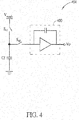
- FIG. 3 and FIG. 4 are schematic diagrams of a charge pump circuit 302 and a pixel circuit 404, respectively.
- the charge pump circuit 302 may be configured to realize the charge pump circuit 102.
- the charge pump circuit 302 comprises switches S 31 -S 34 and a capacitor C.
- the switches S 31 and S 34 are coupled to a first terminal of the capacitor C.
- the switches S 32 and S 33 are coupled to a second terminal of the capacitor C.
- the switches S 31 and S 32 receives a voltage V DD .
- the switch S 33 is coupled to a ground terminal.
- the switch S 34 is configured to output the supply voltage V supply .
- the switches S 31 -S 34 are controlled by the first clock signal clk_1. For example, when the first clock signal clk_1 is high, the switches S 31 and S 33 are conducted, and the switches S 32 and S 34 are cutoff. At this time, the capacitor C is charged by the charge pump circuit 302, which means that the capacitor C is charged up to the voltage V DD . On the other hand, when the first clock signal clk_1 is low, the switches S 32 and S 34 are conducted, and the switches S 31 and S 33 are cutoff. At this time, the supply voltage V supply outputted by the charge pump circuit 302 is 2V DD .
- the pixel circuit 404 may be configured to realize the pixel circuit 104.
- the pixel circuit 404 comprises switches S 41 , S 42 and an integrating circuit 400.
- the switches S 41 and S 42 are coupled to the touch capacitance Cf.
- the switch S 41 receives the supply voltage V supply .
- the switch S 42 is coupled to the integrating circuit 400.
- the switches S 41 and S 42 are controlled by the second clock signal clk_2.
- the pixel clock signal clk_2 is high (corresponding to the sampling interval T s in FIG. 2 )
- the pixel circuit 404 performs a sampling operation, which means that the pixel circuit 404 charges the touch capacitance Cf.
- the pixel circuit 404 may exploit charge sharing to convert the charges stored in the touch capacitance into the pixel output signal Vo via the integrating circuit 400.
- the backend circuit of the pixel circuit 404 may determine whether the location of the pixel circuit 404 is corresponding to a finger ridge or a finger valley according to the pixel output signal Vo.
- the clock generating circuit 100 may generate the second clock signal clk_2, such that when the pixel circuit 104/404 performs the sampling operation (i.e., within the sampling interval T s ), the average V supply of the supply voltage V supply remains the same.
- a pixel clock signal clk_pxl and a charge pump clock signal clk_cp within the pixel circuit do not have direct relationship.
- FIG. 5 is a waveform diagram of the charge pump clock signal clk_cp, the pixel clock signal clk_pxl, a supply voltage V supply ' and a ripple rp' in the art.
- the pixel clock signal clk_pxl and the charge pump clock signal clk_cp are independent clock signals. That is, rising edges of the pixel clock signal clk_pxl and the charge pump clock signal clk_cp do not have certain relationship.
- the pixel clock signal clk_pxl is high (corresponding to the sampling interval T s ')
- the pixel circuit charges the formed touch capacitance.
- the average of the ripple rp' remains not exactly the same.
- the ripple rp' of the charge pump circuit would bring more noise to the fingerprint identification system, and reduce an accuracy of fingerprint identification, such that the overall fingerprint identification performance is reduced.
- the fingerprint identification system 10 may reduce noise effect caused by the ripple rp on the fingerprint identification system 10, and enhance the performance of the fingerprint identification system 10.
- the second period T 2 are not limited to be twice of the first period T1.
- the second period T 2 may be 4 times, 6 times or 8 times of the first period T 1 , i.e., the second period T 2 may be an even multiple of the first period T 1 .
- the sampling interval T s the pixel circuit 104/404 performing the sampling operation is an integer multiple of the first period T 1 , the requirements of the present invention are satisfied.
- the present invention provides the first clock signal and the second clock signal, which are synchronized with each other, to the charge pump circuit and the pixel circuit, respectively, such that when the pixel circuit performs the sampling operation within the sampling interval, the average of the supply voltage generated by the charge pump circuit remains the same.
- the present invention may reduce noise effect of the fingerprint identification system caused by the ripple, and thereby enhance performance of the fingerprint identification system.
Landscapes
- Engineering & Computer Science (AREA)
- Theoretical Computer Science (AREA)
- Human Computer Interaction (AREA)
- Physics & Mathematics (AREA)
- General Physics & Mathematics (AREA)
- Multimedia (AREA)
- Power Engineering (AREA)
- Computer Vision & Pattern Recognition (AREA)
- General Engineering & Computer Science (AREA)
- Measurement Of The Respiration, Hearing Ability, Form, And Blood Characteristics Of Living Organisms (AREA)
- Image Input (AREA)
Abstract
Description
- The present application is a continuation of international application No.
PCT/CN2016/100454, filed on September 27, 2016 - The present invention relates to a fingerprint identification system, and more particularly, to a fingerprint identification system capable of reducing effect caused by ripple.
- With the development of technology, mobile phones, digital cameras, tablet PCs, notebook computers and other portable electronic devices become more and more popular. The portable electronic devices are intended for personal use, with certain privacy. The information stored in the portable device such as phonebook, photos, personal information, etc., are privately owned. If the electronic device is lost, these data may be accessed by other people, causing unnecessary loss. Even though there are several ways using password to protect the electronic device from being used by the other people, the password may be easily to be spread or cracked, which lowers the security. Moreover, the user needs to remember the password so as to use electronic devices. If the user forgets the password, troubles would be brought to the user. Hence, personal fingerprint identification is utilized to achieve the purpose of personal identification, for enhancing the data security.
- In general, the fingerprint identification system utilizes the pixel circuit to receive a finger touch. The pixel circuit would convert a touch capacitance, formed between the pixel circuit and the finger, as the pixel output signal, and the backend circuit of the pixel circuit may determine whether the pixel circuit is corresponding to a finger ridge or a finger valley, according to the pixel output signal. In addition, the power of the pixel circuit is supplied by a charge pump. The pixel circuit receives a pixel clock signal clk_pxl so as to convert the touch capacitance into the pixel output signal. The charge pump circuit receives a charge pump clock signal clk_cp to output a supply voltage Vsupply' to the pixel circuit. Unavoidably, the supply voltage generated by the charge pump circuit has a ripple rp', and a waveform of the ripple rp' is related to the charge pump clock signal clk_cp.
- Generally, the pixel clock signal clk_pxl and the charge pump clock signal clk_cp do not have direct relationship in between. Under a condition that the pixel clock signal clk_pxl is independent of the charge pump clock signal clk_cp, among every sampling interval of the pixel circuit, the average of the ripple rp' is not the same. In this case, the ripple rp' of the charge pump circuit would bring more noise to the fingerprint identification system and reduce an accuracy of the fingerprint identification, such that an overall performance of fingerprint identification is reduced.
- Therefore, how to reduce effect caused by ripple is a significant objective in the field.
- It is therefore a primary objective of the present invention to provide a fingerprint identification system reducing effect caused by ripple, to improve over disadvantages of the prior art.
- To solved the problem stated in the above, the present invention/application provides a fingerprint identification system, comprises a charge pump circuit , configured to generate a supply voltage, wherein the charge pump circuit receives a first clock signal; a pixel circuit, forming a touch capacitance, determining whether the pixel circuit is corresponding to a finger valley or a finger ridge according to the touch capacitance, wherein the pixel circuit receives a second clock signal and the supply voltage; and a clock generating circuit, configured to generate the first clock signal and the second clock signal; wherein the first clock signal is related to the second clock signal.
- Preferably, the clock generating circuit comprises a clock generating unit configured to generate the first clock signal.
- Preferably, the clock generating circuit comprises a frequency divider, coupled to the clock generating unit, configured to generate the second clock signal according to the first clock signal.
- Preferably, a second period of the second clock signal is an even multiple of a first period of the first clock signal.
- Preferably, the second period is twice of the first period.
- Preferably, the first clock signal is synchronized with the second clock signal.
- Preferably, the first clock signal and the second clock signal have rising edges at the same time.
- Preferably, a duty cycle of the first clock signal and the second clock signal is 50%.
- Preferably, the pixel circuit charges the touch capacitance during a sampling interval, and the sampling interval is an integer multiple of a first period of the first clock signal.
- The fingerprint identification system provided by the present invention utilizes the first clock signal and the second clock signal, which are synchronized with each other, such that when the pixel circuit performs the sampling operation within the sampling interval, the average of the supply voltage generated by the charge pump circuit are the same. Therefore, noise effect on the fingerprint identification system caused by the ripple is reduced, and performance of the fingerprint identification system is enhanced.
- These and other objectives of the present invention will no doubt become obvious to those of ordinary skill in the art after reading the following detailed description of the preferred embodiment that is illustrated in the various figures and drawings.
-
-
FIG. 1 is a schematic diagram of a fingerprint identification system according to an embodiment of the present invention. -
FIG. 2 is a waveform diagram of a plurality of signals according to an embodiment of the present invention. -
FIG. 3 is a schematic diagram of a charge pump circuit. -
FIG. 4 is a schematic diagram of a pixel circuit. -
FIG. 5 is a waveform diagram of a plurality of signals. - In order to make the objects, technical solutions and advantages of the present invention become more apparent, the following relies on the accompanying drawings and embodiments to describe the present invention in further detail. It should be understood that the specific embodiments described herein are only for explaining the present invention and are not intended to limit the present invention.
- Please refer to
FIG. 1 andFIG. 2 .FIG. 1 is a schematic diagram of afingerprint identification system 10 according to an embodiment of the present invention.FIG. 2 is a waveform diagram of a first clock signal clk_1, a supply voltage Vsupply, a ripple rp and a second clock signal clk_2. Thefingerprint identification system 10 comprises aclock generating circuit 100, acharge pump circuit 102 and apixel circuit 104. Thepixel circuit 104 forms a touch capacitance Cf with a finger FG. Thepixel circuit 104 may convert the touch capacitance Cf into a pixel output signal Vo, and the backend circuit of the pixel circuit 104 (not illustrated inFIG. 1 ) may determine whether the location at which thepixel circuit 104 locates is corresponding to a finger ridge or a finger valley according to the pixel output signal Vo. Thecharge pump circuit 102 is configured to provide the supply voltage Vsupply for thepixel circuit 104. That is, thecharge pump circuit 102 generates the supply voltage Vsupply to thepixel circuit 104, where the supply voltage Vsupply has a periodical ripple rp. Theclock generating circuit 100, coupled to thecharge pump circuit 102 and thepixel circuit 104, is configured to generate the first clock signal clk_1 to thecharge pump circuit 102 and generate the second clock signal clk_2 to thepixel circuit 104, where the first clock signal clk_1 is related to the second clock signal clk_2. Specifically, as shown inFIG. 2 , the first clock signal clk_1 and the second clock signal clk_2 are signals synchronized with each other. To be more precisely, in an embodiment, a rising edge of the second clock signal clk_2 is aligned to/with a rising edge of the first clock signal clk_1. In addition, the first clock signal clk_1 has a first period T1, and the second clock signal clk_2 has a second period T2. The interval when the second clock signal clk_2 is high (voltage) is corresponding to a sampling interval Ts, and the sampling interval Ts is an integer multiple of the first period T1, i.e., Ts=N T1, where N is a positive integer. - In an embodiment, the first clock signal clk_1 and the second clock signal clk_2 are clock signals with 50% duty cycle. The clock generating
circuit 100 may comprise aclock generating unit 106 and afrequency divider 108. Theclock generating unit 106 is configured to generate the first clock signal clk_1 for thecharge pump circuit 102. Thefrequency divider 108, coupled to theclock generating unit 106, is configured to generate the second clock signal clk_2 for thepixel circuit 104 according to the first clock signal clk_1. Thefrequency divider 108 may generate the second clock signal clk_2, such that the second period T2 (corresponding to the second clock signal clk_2) is twice of the first period T1 (corresponding to the first clock signal clk_1) . That is, the time interval when the second clock signal clk_2 is high voltage is the first period T1 of the first clock signal clk_1 (i.e., Ts=T1, N =1). In this case, among every sampling interval Ts of thepixel circuit 104, the supply voltage Vsupply would have the same averageV supply. Therefore, noise caused by the ripple rp affecting thefingerprint identification system 10 is reduced, and performance of thefingerprint identification system 10 is enhanced. - In addition, implementations of the
charge pump circuit 102 and thepixel circuit 104 are not limited to certain circuit structures. For example, please refer toFIG. 3 andFIG. 4 .FIG. 3 andFIG. 4 are schematic diagrams of acharge pump circuit 302 and apixel circuit 404, respectively. Thecharge pump circuit 302 may be configured to realize thecharge pump circuit 102. As shown inFIG. 3 , thecharge pump circuit 302 comprises switches S31-S34 and a capacitor C. The switches S31 and S34 are coupled to a first terminal of the capacitor C. The switches S32 and S33 are coupled to a second terminal of the capacitor C. The switches S31 and S32 receives a voltage VDD. The switch S33 is coupled to a ground terminal. The switch S34 is configured to output the supply voltage Vsupply. The switches S31-S34 are controlled by the first clock signal clk_1. For example, when the first clock signal clk_1 is high, the switches S31 and S33 are conducted, and the switches S32 and S34 are cutoff. At this time, the capacitor C is charged by thecharge pump circuit 302, which means that the capacitor C is charged up to the voltage VDD. On the other hand, when the first clock signal clk_1 is low, the switches S32 and S34 are conducted, and the switches S31 and S33 are cutoff. At this time, the supply voltage Vsupply outputted by thecharge pump circuit 302 is 2VDD. - In addition, the
pixel circuit 404 may be configured to realize thepixel circuit 104. As shown inFIG. 4 , thepixel circuit 404 comprises switches S41, S42 and an integratingcircuit 400. The switches S41 and S42 are coupled to the touch capacitance Cf. The switch S41 receives the supply voltage Vsupply. The switch S42 is coupled to the integratingcircuit 400. The switches S41 and S42 are controlled by the second clock signal clk_2. When the pixel clock signal clk_2 is high (corresponding to the sampling interval Ts inFIG. 2 ), thepixel circuit 404 performs a sampling operation, which means that thepixel circuit 404 charges the touch capacitance Cf. On the other hand, when the pixel clock signal clk_2 is low, thepixel circuit 404 may exploit charge sharing to convert the charges stored in the touch capacitance into the pixel output signal Vo via the integratingcircuit 400. The backend circuit of thepixel circuit 404 may determine whether the location of thepixel circuit 404 is corresponding to a finger ridge or a finger valley according to the pixel output signal Vo. - As can be seen, the
clock generating circuit 100 may generate the second clock signal clk_2, such that when thepixel circuit 104/404 performs the sampling operation (i.e., within the sampling interval Ts), the averageV supply of the supply voltage Vsupply remains the same. In comparison, in the prior art, a pixel clock signal clk_pxl and a charge pump clock signal clk_cp within the pixel circuit do not have direct relationship. Specifically, please refer toFIG. 5, FIG. 5 is a waveform diagram of the charge pump clock signal clk_cp, the pixel clock signal clk_pxl, a supply voltageV supply' and a ripple rp' in the art. In the art, the pixel clock signal clk_pxl and the charge pump clock signal clk_cp are independent clock signals. That is, rising edges of the pixel clock signal clk_pxl and the charge pump clock signal clk_cp do not have certain relationship. In addition, when the pixel clock signal clk_pxl is high (corresponding to the sampling interval Ts'), the pixel circuit charges the formed touch capacitance. Under a condition that the pixel clock signal clk_pxl is independent of the charge pump clock signal clk_cp, among every sampling interval Ts' of the pixel circuit, the average of the ripple rp' remains not exactly the same. In this case, the ripple rp' of the charge pump circuit would bring more noise to the fingerprint identification system, and reduce an accuracy of fingerprint identification, such that the overall fingerprint identification performance is reduced. In other words, thefingerprint identification system 10 may reduce noise effect caused by the ripple rp on thefingerprint identification system 10, and enhance the performance of thefingerprint identification system 10. - Notably, the embodiments stated in the above are utilized for illustrating the concept of the present invention. Those skilled in the art may make modifications and alterations accordingly, and not limited herein. For example, when the first clock signal clk_1 and the second clock signal clk_2 are clock signals with 50% duty cycle, the second period T2 are not limited to be twice of the first period T1. The second period T2 may be 4 times, 6 times or 8 times of the first period T1, i.e., the second period T2 may be an even multiple of the first period T1. As long as the sampling interval Ts the
pixel circuit 104/404 performing the sampling operation is an integer multiple of the first period T1, the requirements of the present invention are satisfied. - In summary, the present invention provides the first clock signal and the second clock signal, which are synchronized with each other, to the charge pump circuit and the pixel circuit, respectively, such that when the pixel circuit performs the sampling operation within the sampling interval, the average of the supply voltage generated by the charge pump circuit remains the same. Compared to the prior art, the present invention may reduce noise effect of the fingerprint identification system caused by the ripple, and thereby enhance performance of the fingerprint identification system.
- The foregoing is only embodiments of the present application, which is not intended to limit the present application. Any modification following the spirit and principle of the present application, equivalent substitutions, improvements should be included within the scope of the present invention.
Claims (9)
- A fingerprint identification system, characterized in that, the fingerprint identification system comprises:a charge pump circuit , configured to generate a supply voltage, wherein the charge pump circuit receives a first clock signal;a pixel circuit, forming a touch capacitance, configured to determine whether the pixel circuit is corresponding to a finger valley or a finger ridge according to the touch capacitance, wherein the pixel circuit receives a second clock signal and the supply voltage; anda clock generating circuit, configured to generate the first clock signal and the second clock signal;wherein the first clock signal is related to the second clock signal.
- The fingerprint identification system as claim 1, characterized in that, the clock generating circuit comprises a clock generating unit configured to generate the first clock signal.
- The fingerprint identification system as claim 2, characterized in that, the clock generating circuit comprises a frequency divider, coupled to the clock generating unit, configured to generate the second clock signal according to the first clock signal.
- The fingerprint identification system as any of claims 1-3, characterized in that, a second period of the second clock signal is an even multiple of a first period of the first clock signal.
- The fingerprint identification system as claim 4, characterized in that, the second period is twice of the first period.
- The fingerprint identification system as any of claims 1-5, characterized in that, the first clock signal is synchronized with the second clock signal.
- The fingerprint identification system as any of claims 1-6, characterized in that, the first clock signal and the second clock signal have rising edges at the same time.
- The fingerprint identification system as any of claims 1-7, characterized in that, a duty cycle of the first clock signal and the second clock signal is 50%.
- The fingerprint identification system as any of claims 1-8, characterized in that, the pixel circuit charges the touch capacitance during a sampling interval, and the sampling interval is an integer multiple of a first period of the first clock signal.
Applications Claiming Priority (1)
| Application Number | Priority Date | Filing Date | Title |
|---|---|---|---|
| PCT/CN2016/100454 WO2018058337A1 (en) | 2016-09-27 | 2016-09-27 | Fingerprint recognition system |
Publications (3)
| Publication Number | Publication Date |
|---|---|
| EP3327615A1 true EP3327615A1 (en) | 2018-05-30 |
| EP3327615A4 EP3327615A4 (en) | 2018-07-18 |
| EP3327615B1 EP3327615B1 (en) | 2023-09-06 |
Family
ID=58215708
Family Applications (1)
| Application Number | Title | Priority Date | Filing Date |
|---|---|---|---|
| EP16901908.0A Active EP3327615B1 (en) | 2016-09-27 | 2016-09-27 | Fingerprint recognition system |
Country Status (5)
| Country | Link |
|---|---|
| US (1) | US10521638B2 (en) |
| EP (1) | EP3327615B1 (en) |
| KR (1) | KR20180051441A (en) |
| CN (1) | CN106462760B (en) |
| WO (1) | WO2018058337A1 (en) |
Family Cites Families (24)
| Publication number | Priority date | Publication date | Assignee | Title |
|---|---|---|---|---|
| AU2003254280A1 (en) * | 2002-08-02 | 2004-02-23 | Cross Match Technologies, Inc. | System and method for counting ridges in a captured print image |
| DE602005013401D1 (en) * | 2004-07-22 | 2009-04-30 | Nec Corp | IMAGE PROCESSING SYSTEM |
| RU2361272C2 (en) * | 2005-01-31 | 2009-07-10 | Присайз Биометрикс Аб | Method and device for improved identification of fingerprints |
| US8116540B2 (en) * | 2008-04-04 | 2012-02-14 | Validity Sensors, Inc. | Apparatus and method for reducing noise in fingerprint sensing circuits |
| KR20090106816A (en) * | 2008-04-07 | 2009-10-12 | 삼성전자주식회사 | Clock Driver and Charge Pump With the Same |
| US8164367B1 (en) * | 2009-01-15 | 2012-04-24 | Integrated Device Technology, Inc. | Spread spectrum clock generation technique for imaging applications |
| CN102055467B (en) * | 2009-11-05 | 2013-02-06 | 晨星软件研发(深圳)有限公司 | Phase Locked Loop and Its Related Methods |
| US20110168782A1 (en) * | 2010-01-12 | 2011-07-14 | Nxp B.V. | Capacitance under a fringe capacitor of a radio frquency integrated circuit |
| JP5427648B2 (en) * | 2010-03-02 | 2014-02-26 | 株式会社ジャパンディスプレイ | Coordinate input device and display device including the same |
| US8710956B2 (en) * | 2011-06-06 | 2014-04-29 | Leonard P. Longo | Fingerprinting apparatus, system, and method |
| US8982090B2 (en) * | 2012-01-01 | 2015-03-17 | Cypress Semiconductor Corporation | Optical stylus synchronization |
| US10503948B2 (en) * | 2014-03-06 | 2019-12-10 | Qualcomm Incorporated | Multi-spectral ultrasonic imaging |
| US20160033988A1 (en) * | 2014-07-31 | 2016-02-04 | Semiconductor Components Industries, Llc | Power converter using charge pump divider and method therefor |
| TWI526945B (en) * | 2014-08-26 | 2016-03-21 | 神盾股份有限公司 | Capacitive fingerprint sensing device and fingerprint sensing method thereof |
| CN104298962B (en) * | 2014-09-04 | 2018-04-27 | 深圳市汇顶科技股份有限公司 | Finger print detection device and method |
| KR101659492B1 (en) | 2014-11-10 | 2016-09-23 | 한신대학교 산학협력단 | Charge Transfer Circuit for Capacitive Sensing and Apparatus For Detecting Fingerprint Having Thereof |
| US9491151B2 (en) * | 2015-01-07 | 2016-11-08 | Ememory Technology Inc. | Memory apparatus, charge pump circuit and voltage pumping method thereof |
| CN105046192A (en) * | 2015-05-21 | 2015-11-11 | 广东光阵光电科技有限公司 | An identification control method and device for a fingerprint identification module |
| CN106971149A (en) * | 2015-07-24 | 2017-07-21 | 深圳市汇顶科技股份有限公司 | Fingerprint detection circuit and fingerprint identification system |
| CN106980824A (en) * | 2015-07-27 | 2017-07-25 | 深圳市汇顶科技股份有限公司 | Fingerprint detection circuit and fingerprint identification system |
| KR20170024664A (en) * | 2015-08-26 | 2017-03-08 | 삼성전기주식회사 | Apparatus for sensing touch input |
| CN107004126A (en) * | 2015-11-02 | 2017-08-01 | 深圳市汇顶科技股份有限公司 | Multifunctional fingerprint sensor with anti-fingerprint spoofing optical sensing |
| KR102586120B1 (en) * | 2016-09-23 | 2023-10-06 | 엘지디스플레이 주식회사 | Touch driving circuit, touch display device and method for driving thereof |
| EP3321848B1 (en) * | 2016-09-27 | 2019-12-25 | Shenzhen Goodix Technology Co., Ltd. | Capacitive sensing circuit |
-
2016
- 2016-09-27 KR KR1020177035380A patent/KR20180051441A/en not_active Ceased
- 2016-09-27 WO PCT/CN2016/100454 patent/WO2018058337A1/en not_active Ceased
- 2016-09-27 CN CN201680001058.5A patent/CN106462760B/en active Active
- 2016-09-27 EP EP16901908.0A patent/EP3327615B1/en active Active
-
2017
- 2017-11-21 US US15/820,390 patent/US10521638B2/en active Active
Also Published As
| Publication number | Publication date |
|---|---|
| US10521638B2 (en) | 2019-12-31 |
| KR20180051441A (en) | 2018-05-16 |
| EP3327615A4 (en) | 2018-07-18 |
| US20180096185A1 (en) | 2018-04-05 |
| CN106462760B (en) | 2019-12-17 |
| CN106462760A (en) | 2017-02-22 |
| WO2018058337A1 (en) | 2018-04-05 |
| EP3327615B1 (en) | 2023-09-06 |
Similar Documents
| Publication | Publication Date | Title |
|---|---|---|
| CN107077610B (en) | Capacitance interpretation circuit and fingerprint identification system | |
| US10346668B2 (en) | Capacitive sensing circuit | |
| US10565420B2 (en) | Capacitive sensing circuit | |
| US10496869B2 (en) | Fingerprint detection circuit and fingerprint recognition system | |
| CN106462758B (en) | Fingerprint identification system and electronic device | |
| US20170243044A1 (en) | Signal conversion circuit and fingerprint identification system | |
| US10380401B2 (en) | Capacitance sensing circuit and fingerprint identification system | |
| US20150188344A1 (en) | Charging and discharging control system and method for battery | |
| US10521638B2 (en) | Fingerprint identification system | |
| HK1221318A1 (en) | Fingerprint recognition system | |
| US10650215B2 (en) | Fingerprint sensor and terminal device | |
| EP3206159A1 (en) | Output conversion circuit and fingerprint recognition system | |
| CN112701758A (en) | Charging current setting method and system and mobile terminal | |
| CN115146747A (en) | Digital temperature sensor and passive radio frequency tag containing the same | |
| UA123194U (en) | MOBILE COMPUTER TERMINAL "K.VRT800" |
Legal Events
| Date | Code | Title | Description |
|---|---|---|---|
| STAA | Information on the status of an ep patent application or granted ep patent |
Free format text: STATUS: UNKNOWN |
|
| STAA | Information on the status of an ep patent application or granted ep patent |
Free format text: STATUS: THE INTERNATIONAL PUBLICATION HAS BEEN MADE |
|
| PUAI | Public reference made under article 153(3) epc to a published international application that has entered the european phase |
Free format text: ORIGINAL CODE: 0009012 |
|
| STAA | Information on the status of an ep patent application or granted ep patent |
Free format text: STATUS: REQUEST FOR EXAMINATION WAS MADE |
|
| 17P | Request for examination filed |
Effective date: 20171123 |
|
| AK | Designated contracting states |
Kind code of ref document: A1 Designated state(s): AL AT BE BG CH CY CZ DE DK EE ES FI FR GB GR HR HU IE IS IT LI LT LU LV MC MK MT NL NO PL PT RO RS SE SI SK SM TR |
|
| AX | Request for extension of the european patent |
Extension state: BA ME |
|
| A4 | Supplementary search report drawn up and despatched |
Effective date: 20180615 |
|
| RIC1 | Information provided on ipc code assigned before grant |
Ipc: G06F 3/044 20060101ALI20180611BHEP Ipc: G06K 9/00 20060101AFI20180611BHEP Ipc: H02M 1/14 20060101ALI20180611BHEP Ipc: H02M 3/07 20060101ALI20180611BHEP |
|
| DAV | Request for validation of the european patent (deleted) | ||
| DAX | Request for extension of the european patent (deleted) | ||
| STAA | Information on the status of an ep patent application or granted ep patent |
Free format text: STATUS: EXAMINATION IS IN PROGRESS |
|
| 17Q | First examination report despatched |
Effective date: 20210330 |
|
| REG | Reference to a national code |
Ref country code: DE Ref legal event code: R079 Free format text: PREVIOUS MAIN CLASS: G06K0009000000 Ipc: G06V0040130000 Ref country code: DE Ref legal event code: R079 Ref document number: 602016082661 Country of ref document: DE Free format text: PREVIOUS MAIN CLASS: G06K0009000000 Ipc: G06V0040130000 |
|
| GRAP | Despatch of communication of intention to grant a patent |
Free format text: ORIGINAL CODE: EPIDOSNIGR1 |
|
| STAA | Information on the status of an ep patent application or granted ep patent |
Free format text: STATUS: GRANT OF PATENT IS INTENDED |
|
| RIC1 | Information provided on ipc code assigned before grant |
Ipc: H02M 3/07 20060101ALI20230420BHEP Ipc: H02M 1/14 20060101ALI20230420BHEP Ipc: G06V 40/12 20220101ALI20230420BHEP Ipc: G06V 40/13 20220101AFI20230420BHEP |
|
| INTG | Intention to grant announced |
Effective date: 20230508 |
|
| GRAS | Grant fee paid |
Free format text: ORIGINAL CODE: EPIDOSNIGR3 |
|
| GRAA | (expected) grant |
Free format text: ORIGINAL CODE: 0009210 |
|
| STAA | Information on the status of an ep patent application or granted ep patent |
Free format text: STATUS: THE PATENT HAS BEEN GRANTED |
|
| AK | Designated contracting states |
Kind code of ref document: B1 Designated state(s): AL AT BE BG CH CY CZ DE DK EE ES FI FR GB GR HR HU IE IS IT LI LT LU LV MC MK MT NL NO PL PT RO RS SE SI SK SM TR |
|
| REG | Reference to a national code |
Ref country code: GB Ref legal event code: FG4D |
|
| REG | Reference to a national code |
Ref country code: CH Ref legal event code: EP |
|
| REG | Reference to a national code |
Ref country code: IE Ref legal event code: FG4D |
|
| REG | Reference to a national code |
Ref country code: DE Ref legal event code: R096 Ref document number: 602016082661 Country of ref document: DE |
|
| REG | Reference to a national code |
Ref country code: LT Ref legal event code: MG9D |
|
| REG | Reference to a national code |
Ref country code: NL Ref legal event code: MP Effective date: 20230906 |
|
| PG25 | Lapsed in a contracting state [announced via postgrant information from national office to epo] |
Ref country code: GR Free format text: LAPSE BECAUSE OF FAILURE TO SUBMIT A TRANSLATION OF THE DESCRIPTION OR TO PAY THE FEE WITHIN THE PRESCRIBED TIME-LIMIT Effective date: 20231207 |
|
| PG25 | Lapsed in a contracting state [announced via postgrant information from national office to epo] |
Ref country code: SE Free format text: LAPSE BECAUSE OF FAILURE TO SUBMIT A TRANSLATION OF THE DESCRIPTION OR TO PAY THE FEE WITHIN THE PRESCRIBED TIME-LIMIT Effective date: 20230906 Ref country code: RS Free format text: LAPSE BECAUSE OF FAILURE TO SUBMIT A TRANSLATION OF THE DESCRIPTION OR TO PAY THE FEE WITHIN THE PRESCRIBED TIME-LIMIT Effective date: 20230906 Ref country code: NO Free format text: LAPSE BECAUSE OF FAILURE TO SUBMIT A TRANSLATION OF THE DESCRIPTION OR TO PAY THE FEE WITHIN THE PRESCRIBED TIME-LIMIT Effective date: 20231206 Ref country code: LV Free format text: LAPSE BECAUSE OF FAILURE TO SUBMIT A TRANSLATION OF THE DESCRIPTION OR TO PAY THE FEE WITHIN THE PRESCRIBED TIME-LIMIT Effective date: 20230906 Ref country code: LT Free format text: LAPSE BECAUSE OF FAILURE TO SUBMIT A TRANSLATION OF THE DESCRIPTION OR TO PAY THE FEE WITHIN THE PRESCRIBED TIME-LIMIT Effective date: 20230906 Ref country code: HR Free format text: LAPSE BECAUSE OF FAILURE TO SUBMIT A TRANSLATION OF THE DESCRIPTION OR TO PAY THE FEE WITHIN THE PRESCRIBED TIME-LIMIT Effective date: 20230906 Ref country code: GR Free format text: LAPSE BECAUSE OF FAILURE TO SUBMIT A TRANSLATION OF THE DESCRIPTION OR TO PAY THE FEE WITHIN THE PRESCRIBED TIME-LIMIT Effective date: 20231207 Ref country code: FI Free format text: LAPSE BECAUSE OF FAILURE TO SUBMIT A TRANSLATION OF THE DESCRIPTION OR TO PAY THE FEE WITHIN THE PRESCRIBED TIME-LIMIT Effective date: 20230906 |
|
| REG | Reference to a national code |
Ref country code: AT Ref legal event code: MK05 Ref document number: 1609578 Country of ref document: AT Kind code of ref document: T Effective date: 20230906 |
|
| PG25 | Lapsed in a contracting state [announced via postgrant information from national office to epo] |
Ref country code: NL Free format text: LAPSE BECAUSE OF FAILURE TO SUBMIT A TRANSLATION OF THE DESCRIPTION OR TO PAY THE FEE WITHIN THE PRESCRIBED TIME-LIMIT Effective date: 20230906 |
|
| PG25 | Lapsed in a contracting state [announced via postgrant information from national office to epo] |
Ref country code: IS Free format text: LAPSE BECAUSE OF FAILURE TO SUBMIT A TRANSLATION OF THE DESCRIPTION OR TO PAY THE FEE WITHIN THE PRESCRIBED TIME-LIMIT Effective date: 20240106 |
|
| PG25 | Lapsed in a contracting state [announced via postgrant information from national office to epo] |
Ref country code: AT Free format text: LAPSE BECAUSE OF FAILURE TO SUBMIT A TRANSLATION OF THE DESCRIPTION OR TO PAY THE FEE WITHIN THE PRESCRIBED TIME-LIMIT Effective date: 20230906 |
|
| PG25 | Lapsed in a contracting state [announced via postgrant information from national office to epo] |
Ref country code: ES Free format text: LAPSE BECAUSE OF FAILURE TO SUBMIT A TRANSLATION OF THE DESCRIPTION OR TO PAY THE FEE WITHIN THE PRESCRIBED TIME-LIMIT Effective date: 20230906 |
|
| PG25 | Lapsed in a contracting state [announced via postgrant information from national office to epo] |
Ref country code: SM Free format text: LAPSE BECAUSE OF FAILURE TO SUBMIT A TRANSLATION OF THE DESCRIPTION OR TO PAY THE FEE WITHIN THE PRESCRIBED TIME-LIMIT Effective date: 20230906 Ref country code: RO Free format text: LAPSE BECAUSE OF FAILURE TO SUBMIT A TRANSLATION OF THE DESCRIPTION OR TO PAY THE FEE WITHIN THE PRESCRIBED TIME-LIMIT Effective date: 20230906 Ref country code: IS Free format text: LAPSE BECAUSE OF FAILURE TO SUBMIT A TRANSLATION OF THE DESCRIPTION OR TO PAY THE FEE WITHIN THE PRESCRIBED TIME-LIMIT Effective date: 20240106 Ref country code: ES Free format text: LAPSE BECAUSE OF FAILURE TO SUBMIT A TRANSLATION OF THE DESCRIPTION OR TO PAY THE FEE WITHIN THE PRESCRIBED TIME-LIMIT Effective date: 20230906 Ref country code: EE Free format text: LAPSE BECAUSE OF FAILURE TO SUBMIT A TRANSLATION OF THE DESCRIPTION OR TO PAY THE FEE WITHIN THE PRESCRIBED TIME-LIMIT Effective date: 20230906 Ref country code: CZ Free format text: LAPSE BECAUSE OF FAILURE TO SUBMIT A TRANSLATION OF THE DESCRIPTION OR TO PAY THE FEE WITHIN THE PRESCRIBED TIME-LIMIT Effective date: 20230906 Ref country code: AT Free format text: LAPSE BECAUSE OF FAILURE TO SUBMIT A TRANSLATION OF THE DESCRIPTION OR TO PAY THE FEE WITHIN THE PRESCRIBED TIME-LIMIT Effective date: 20230906 Ref country code: SK Free format text: LAPSE BECAUSE OF FAILURE TO SUBMIT A TRANSLATION OF THE DESCRIPTION OR TO PAY THE FEE WITHIN THE PRESCRIBED TIME-LIMIT Effective date: 20230906 Ref country code: PT Free format text: LAPSE BECAUSE OF FAILURE TO SUBMIT A TRANSLATION OF THE DESCRIPTION OR TO PAY THE FEE WITHIN THE PRESCRIBED TIME-LIMIT Effective date: 20240108 |
|
| REG | Reference to a national code |
Ref country code: CH Ref legal event code: PL |
|
| PG25 | Lapsed in a contracting state [announced via postgrant information from national office to epo] |
Ref country code: LU Free format text: LAPSE BECAUSE OF NON-PAYMENT OF DUE FEES Effective date: 20230927 |
|
| REG | Reference to a national code |
Ref country code: BE Ref legal event code: MM Effective date: 20230930 |
|
| PG25 | Lapsed in a contracting state [announced via postgrant information from national office to epo] |
Ref country code: PL Free format text: LAPSE BECAUSE OF FAILURE TO SUBMIT A TRANSLATION OF THE DESCRIPTION OR TO PAY THE FEE WITHIN THE PRESCRIBED TIME-LIMIT Effective date: 20230906 Ref country code: LU Free format text: LAPSE BECAUSE OF NON-PAYMENT OF DUE FEES Effective date: 20230927 Ref country code: IT Free format text: LAPSE BECAUSE OF FAILURE TO SUBMIT A TRANSLATION OF THE DESCRIPTION OR TO PAY THE FEE WITHIN THE PRESCRIBED TIME-LIMIT Effective date: 20230906 |
|
| REG | Reference to a national code |
Ref country code: DE Ref legal event code: R097 Ref document number: 602016082661 Country of ref document: DE |
|
| PG25 | Lapsed in a contracting state [announced via postgrant information from national office to epo] |
Ref country code: MC Free format text: LAPSE BECAUSE OF FAILURE TO SUBMIT A TRANSLATION OF THE DESCRIPTION OR TO PAY THE FEE WITHIN THE PRESCRIBED TIME-LIMIT Effective date: 20230906 |
|
| REG | Reference to a national code |
Ref country code: IE Ref legal event code: MM4A |
|
| PG25 | Lapsed in a contracting state [announced via postgrant information from national office to epo] |
Ref country code: IE Free format text: LAPSE BECAUSE OF NON-PAYMENT OF DUE FEES Effective date: 20230927 |
|
| PG25 | Lapsed in a contracting state [announced via postgrant information from national office to epo] |
Ref country code: DK Free format text: LAPSE BECAUSE OF FAILURE TO SUBMIT A TRANSLATION OF THE DESCRIPTION OR TO PAY THE FEE WITHIN THE PRESCRIBED TIME-LIMIT Effective date: 20230906 |
|
| PLBE | No opposition filed within time limit |
Free format text: ORIGINAL CODE: 0009261 |
|
| STAA | Information on the status of an ep patent application or granted ep patent |
Free format text: STATUS: NO OPPOSITION FILED WITHIN TIME LIMIT |
|
| PG25 | Lapsed in a contracting state [announced via postgrant information from national office to epo] |
Ref country code: CH Free format text: LAPSE BECAUSE OF NON-PAYMENT OF DUE FEES Effective date: 20230930 |
|
| PG25 | Lapsed in a contracting state [announced via postgrant information from national office to epo] |
Ref country code: MC Free format text: LAPSE BECAUSE OF FAILURE TO SUBMIT A TRANSLATION OF THE DESCRIPTION OR TO PAY THE FEE WITHIN THE PRESCRIBED TIME-LIMIT Effective date: 20230906 Ref country code: IE Free format text: LAPSE BECAUSE OF NON-PAYMENT OF DUE FEES Effective date: 20230927 Ref country code: DK Free format text: LAPSE BECAUSE OF FAILURE TO SUBMIT A TRANSLATION OF THE DESCRIPTION OR TO PAY THE FEE WITHIN THE PRESCRIBED TIME-LIMIT Effective date: 20230906 Ref country code: CH Free format text: LAPSE BECAUSE OF NON-PAYMENT OF DUE FEES Effective date: 20230930 Ref country code: SI Free format text: LAPSE BECAUSE OF FAILURE TO SUBMIT A TRANSLATION OF THE DESCRIPTION OR TO PAY THE FEE WITHIN THE PRESCRIBED TIME-LIMIT Effective date: 20230906 |
|
| 26N | No opposition filed |
Effective date: 20240607 |
|
| PG25 | Lapsed in a contracting state [announced via postgrant information from national office to epo] |
Ref country code: BE Free format text: LAPSE BECAUSE OF NON-PAYMENT OF DUE FEES Effective date: 20230930 |
|
| PG25 | Lapsed in a contracting state [announced via postgrant information from national office to epo] |
Ref country code: FR Free format text: LAPSE BECAUSE OF NON-PAYMENT OF DUE FEES Effective date: 20231106 |
|
| PG25 | Lapsed in a contracting state [announced via postgrant information from national office to epo] |
Ref country code: FR Free format text: LAPSE BECAUSE OF NON-PAYMENT OF DUE FEES Effective date: 20231106 |
|
| PG25 | Lapsed in a contracting state [announced via postgrant information from national office to epo] |
Ref country code: BG Free format text: LAPSE BECAUSE OF FAILURE TO SUBMIT A TRANSLATION OF THE DESCRIPTION OR TO PAY THE FEE WITHIN THE PRESCRIBED TIME-LIMIT Effective date: 20230906 |
|
| PG25 | Lapsed in a contracting state [announced via postgrant information from national office to epo] |
Ref country code: BG Free format text: LAPSE BECAUSE OF FAILURE TO SUBMIT A TRANSLATION OF THE DESCRIPTION OR TO PAY THE FEE WITHIN THE PRESCRIBED TIME-LIMIT Effective date: 20230906 |
|
| REG | Reference to a national code |
Ref country code: DE Ref legal event code: R082 Ref document number: 602016082661 Country of ref document: DE Representative=s name: KBN IP PATENTANWAELTE PARTNERSCHAFT MBB, DE |
|
| PG25 | Lapsed in a contracting state [announced via postgrant information from national office to epo] |
Ref country code: CY Free format text: LAPSE BECAUSE OF FAILURE TO SUBMIT A TRANSLATION OF THE DESCRIPTION OR TO PAY THE FEE WITHIN THE PRESCRIBED TIME-LIMIT; INVALID AB INITIO Effective date: 20160927 |
|
| PG25 | Lapsed in a contracting state [announced via postgrant information from national office to epo] |
Ref country code: HU Free format text: LAPSE BECAUSE OF FAILURE TO SUBMIT A TRANSLATION OF THE DESCRIPTION OR TO PAY THE FEE WITHIN THE PRESCRIBED TIME-LIMIT; INVALID AB INITIO Effective date: 20160927 |
|
| PGFP | Annual fee paid to national office [announced via postgrant information from national office to epo] |
Ref country code: DE Payment date: 20250819 Year of fee payment: 10 |
|
| PGFP | Annual fee paid to national office [announced via postgrant information from national office to epo] |
Ref country code: GB Payment date: 20250814 Year of fee payment: 10 |
|
| PG25 | Lapsed in a contracting state [announced via postgrant information from national office to epo] |
Ref country code: TR Free format text: LAPSE BECAUSE OF FAILURE TO SUBMIT A TRANSLATION OF THE DESCRIPTION OR TO PAY THE FEE WITHIN THE PRESCRIBED TIME-LIMIT Effective date: 20230906 |