EP3327454A1 - Battery system with a shared cell supervision circuit unit - Google Patents
Battery system with a shared cell supervision circuit unit Download PDFInfo
- Publication number
- EP3327454A1 EP3327454A1 EP16200852.8A EP16200852A EP3327454A1 EP 3327454 A1 EP3327454 A1 EP 3327454A1 EP 16200852 A EP16200852 A EP 16200852A EP 3327454 A1 EP3327454 A1 EP 3327454A1
- Authority
- EP
- European Patent Office
- Prior art keywords
- bus bar
- battery system
- terminal
- battery
- circuit unit
- Prior art date
- Legal status (The legal status is an assumption and is not a legal conclusion. Google has not performed a legal analysis and makes no representation as to the accuracy of the status listed.)
- Granted
Links
Images



Classifications
-
- G—PHYSICS
- G01—MEASURING; TESTING
- G01R—MEASURING ELECTRIC VARIABLES; MEASURING MAGNETIC VARIABLES
- G01R31/00—Arrangements for testing electric properties; Arrangements for locating electric faults; Arrangements for electrical testing characterised by what is being tested not provided for elsewhere
- G01R31/36—Arrangements for testing, measuring or monitoring the electrical condition of accumulators or electric batteries, e.g. capacity or state of charge [SoC]
- G01R31/382—Arrangements for monitoring battery or accumulator variables, e.g. SoC
- G01R31/3835—Arrangements for monitoring battery or accumulator variables, e.g. SoC involving only voltage measurements
-
- G—PHYSICS
- G01—MEASURING; TESTING
- G01R—MEASURING ELECTRIC VARIABLES; MEASURING MAGNETIC VARIABLES
- G01R31/00—Arrangements for testing electric properties; Arrangements for locating electric faults; Arrangements for electrical testing characterised by what is being tested not provided for elsewhere
- G01R31/36—Arrangements for testing, measuring or monitoring the electrical condition of accumulators or electric batteries, e.g. capacity or state of charge [SoC]
- G01R31/382—Arrangements for monitoring battery or accumulator variables, e.g. SoC
-
- G—PHYSICS
- G01—MEASURING; TESTING
- G01R—MEASURING ELECTRIC VARIABLES; MEASURING MAGNETIC VARIABLES
- G01R31/00—Arrangements for testing electric properties; Arrangements for locating electric faults; Arrangements for electrical testing characterised by what is being tested not provided for elsewhere
- G01R31/36—Arrangements for testing, measuring or monitoring the electrical condition of accumulators or electric batteries, e.g. capacity or state of charge [SoC]
- G01R31/392—Determining battery ageing or deterioration, e.g. state of health
-
- G—PHYSICS
- G01—MEASURING; TESTING
- G01R—MEASURING ELECTRIC VARIABLES; MEASURING MAGNETIC VARIABLES
- G01R31/00—Arrangements for testing electric properties; Arrangements for locating electric faults; Arrangements for electrical testing characterised by what is being tested not provided for elsewhere
- G01R31/36—Arrangements for testing, measuring or monitoring the electrical condition of accumulators or electric batteries, e.g. capacity or state of charge [SoC]
- G01R31/396—Acquisition or processing of data for testing or for monitoring individual cells or groups of cells within a battery
Definitions
- the present invention relates to a battery system which comprises a first and a second battery module, comprising at least one battery cell and a first and a second terminal respectively.
- the battery system further comprises a first bus bar, electrically connecting the first terminal of the first battery module with the terminal of another battery module and/or with a potential of the battery system.
- the battery system comprises a second bus bar, electrically connecting the second terminal of the first battery module with the first terminal of the second battery module.
- the battery system comprises a Cell Supervision Circuit Unit with a plurality of input channels, wherein the first and second terminal of the first and second battery module are connected to one of the plurality of input channels respectively, the first terminal of the first battery module being connected to a GND-input channel.
- a rechargeable or secondary battery system differs from a primary battery system in that it can be repeatedly charged and discharged, while the latter provides only an irreversible conversion of chemical to electrical energy.
- Low-capacity rechargeable battery systems are used as power supply for small electronic devices, such as cellular phones, notebook computers and camcorders, while high-capacity rechargeable battery systems are used as the power supply for hybrid vehicles and the like.
- battery systems comprise a plurality of battery modules, wherein the battery modules comprise a plurality of battery cells.
- the battery cells of a battery module are controlled and supervised with regard to a plurality of different parameters, as for example their respective State of Charge (SoC), temperature and output voltage via so called Cell Supervision Circuit Units (CSC).
- SoC State of Charge
- CSC Cell Supervision Circuit Units
- Such Cell Supervision Circuits or Cell Supervision Circuit Units often are realized as Analog-Front-End (AFE) chips and/or as printed circuit boards (PCB) that are available having 6, 12 or 18 input channels respectively.
- AFE Analog-Front-End
- PCB printed circuit boards
- one Cell Supervision Circuit Unit is allocated to one battery module respectively.
- CSC Cell Supervision Circuit Unit
- a battery system 300 of the state of the art is shown in figure 1 .
- the battery system 300 comprises six battery modules, each battery module comprising a plurality of battery cells 10 and an own Cell Supervision Circuit Unit 50 respectively.
- the input channels of the Cell Supervision Circuit Units 50 of the battery modules are electrically connected to the battery cells 10 of the respective corresponding battery module.
- the battery system 300 shown in figure 1 exemplarily comprises a battery management unit 255 which is connected to the first of the battery modules 1 via a connector 256 of the battery management unit 255.
- the first terminal 11-1 of the first battery module 1 is electrically connected to a predefined potential 4 which in this example is exemplarily equal to the potential of a plus pole of the battery system 300.
- the second terminal 11-2 of the first battery module 1 is electrically connected to the first terminal 12-1 of the second battery module 2 of the six battery modules.
- the first and the second bus bars 100, 200 are exemplarily realized as metal stripes or bars which are formed to electrically interconnect the aforementioned terminals 11-1, 11-2, 12-1, 12-2.
- the remaining battery modules are electrically interconnected in series.
- a battery system comprises a first and a second battery module, comprising at least one battery cell and a first and a second terminal respectively. Furthermore, the battery system comprises a first bus bar, electrically connecting the first terminal of the first battery module with the terminal of another battery module and/or with a potential of the battery system. Moreover, the battery system comprises a second bus bar, electrically connecting the second terminal of the first battery module with the first terminal of the second battery module.
- the battery system further comprises a Cell Supervision Circuit Unit with a plurality of input channels, wherein the first and second terminal of the first and second battery module are connected to one of the plurality of input channels respectively, the first terminal of the first battery module being connected to a GND-input channel.
- the Cell Supervision Circuit Unit is adapted to measure the voltage drop across the first bus bar.
- the Cell Supervision Circuit Unit was used to control and supervise the battery cells also of the second battery module, this control/supervision would be performed erroneously, as the voltage drop across the second bus bar would not be considered by the Cell Supervision Circuit Unit. It is not possible to simply measure the voltages that drop across the second bus bar with one separate channel of the Cell Supervision Circuit Unit, as it is not possible to measure negative voltages with the same. However, when the voltage drop across the second and the further bus bars of a battery system is calculated, the calculated voltages can be taken into account by a Cell Supervision Circuit Unit, thus allowing for the same to control and supervise a plurality of battery modules - and the battery cells thereof - interconnected via bus bars. Expressed in other words, the invention allows for the usage of a shared Cell Supervision Circuit Unit for a plurality of battery modules, interconnected via multiple connectors/bus bars.
- a bus bar is a conductive strip or bar that conducts electricity within a battery system, electrically interconnecting the terminals of battery modules and/or of battery cells and/or of electrical apparatuses and components.
- the bus bar is a conductive metallic strip or bar.
- the GND-input channel is a ground input channel or an input channel for a ground potential.
- a Cell Supervision Circuit Unit is equal to a full Cell Supervision Circuit.
- the potential of the battery system is equal to a ground potential, to the potential of a plus pole or to the potential of a minus pole of the battery system. Furthermore preferred, the potential of the battery system is substantially equal to a ground potential, to the potential of a plus pole or to the potential of a minus pole of the battery system.
- a terminal of a battery module is formed by a terminal of a battery cell of the respective battery module.
- the first terminal of the first battery module is formed by a terminal of a battery cell of the first battery module.
- the Cell Supervision Circuit Unit is realized as a chip or a chipset.
- the Cell Supervision Circuit Unit has six input channels. Even more preferred, the Cell Supervision Circuit Unit has 12 input channels. In such an embodiment, the maximum number of cells that can be handled by a single Cell Supervision Circuit Unit is 12.
- the Cell Supervision Circuit Unit has 18 input channels. In many applications - as for example in electric vehicle (EV) applications - the number of serial connected battery cells per battery module is low, which is due to a high number of parallel battery cell connections. Therefore it is possible to use a single Cell Supervision Circuit Unit for more than one battery module.
- EV electric vehicle
- the first terminal of the first battery module is connected to a GND-input channel of the Cell Supervision Circuit Unit.
- the battery system further comprises an electronic circuit, adapted to calculate the voltage drop across the second bus bar, using the measured voltage drop across the first bus bar.
- an electronic circuit adapted to calculate the voltage drop across the second bus bar, using the measured voltage drop across the first bus bar.
- it is possible to precisely calculate the voltage dropping across the bus bars coming to use within the battery system. This allows for a significant reduction of costs.
- the accuracy is increased.
- the voltage drop over the further bus bars is measured with an additional input channel of the Cell Supervision Circuit Unit, there is no risk of a negative voltage being supplied to an input of a battery management system chip which may damage the same through an overvoltage.
- the invention allows for the usage of a single Cell Supervision Circuit Unit to supervise/control multiple battery modules of the battery system and thus to significantly decrease the number of Cell Supervision Circuit Units coming to use within the battery system. Therefore, the costs of production and the power consumption of the battery system are significantly decreased and the energy efficiency of the battery system is significantly increased.
- the voltage drops across the bus bars are known, the voltages of the different cells of the battery modules can be measured and adjusted accordingly by the Cell Supervision Circuit Unit coming to use.
- the electronic circuit is adapted to calculate the voltage drop across the second bus bar as a function of the measured voltage drop across the first bus bar and of at least one geometrical parameter of the second bus bar.
- the same current flows through every bus bar. Therefore, the voltage drop across a bus bar should substantially be the same for same dimensions - apart from negligible influence of the temperature. If a bus bar is twice as long as the another bus bar - and the other dimensions as width and height of the bus bars are the same - the voltage dropping across this bus bar is also doubled. Due to this reason the voltage drop can be calculated for different lengths of bus bars, when the voltage drop of one bus bar is known.
- the width and height of the first and the second bus bar are identical or substantially identical.
- the at least one geometrical parameter is chosen out of a group of parameters, the group of parameters comprising the length of the second bus bar, the width of the second bus bar and the height of the second bus bar.
- the calculation of the voltage drops across the other bus bars can be performed in a highly accurate manner.
- the electronic circuit is adapted to calculate the voltage drop across the second bus bar as a function of the measured voltage drop across the first bus bar and of at least one parameter of the second bus bar.
- the at least one parameter is the material of the second bus bar.
- the electronic circuit is adapted to consider and/or calculate the inductivity of the bus bar in order to calculate the voltage dropping across the second bus bar.
- the electronic circuit is further adapted to consider and/or calculate the ohmic resistance of the second bus bar in order to calculate the voltage dropping across the second bus bar, wherein the cross section, the length and/or the material of the second bus bar is considered.
- the first and second bus bars comprise copper.
- the ratio I BB /R is constant for all the bus bars of the battery system.
- At least one input filter especially a low-pass filter is used to reduce the measured voltage drop due to the inductance of the bus bar.
- the voltage drop across the bus bars is not linearly scalable due to the length of the bus bars respectively.
- the linearity of the calculated inductance can be changed/transferred to an insignificant value.
- the inductive, not scalable part of the impedance is suppressed to an insignificant value.
- the voltage drop is linearly scalable and the incorrectly measured cell voltage can be corrected.
- the electronic circuit is integrated within the Cell Supervision Circuit Unit.
- the battery system is even more compact, as the electronic circuit which is allowing for the omittance of a plurality of Cell Supervision Circuit Units is integrated within the one Cell Supervision Circuit Unit that is maintained within the battery system and thus does not require a lot of additional space.
- the electronic circuit comprises a processing unit.
- a processing unit allows for quick and accurate calculations.
- the processing unit is realized as a microcontroller or a microprocessor.
- the battery system further comprises a level shifter circuit electrically connected to the Cell Supervision Circuit Unit and/or to the first and/or second battery module.
- the level shifter circuit can be used to measure positive and negative voltages, preventing negative voltages from directly being supplied to the input channels of the Cell Supervision Circuit Unit and thus from destroying the Cell Supervision Circuit Unit.
- the level shifter circuit is a part of the electronic circuit. Furthermore preferred, the level shifter circuit is a part of the Cell Supervision Circuit Unit.
- the level shifter circuit comprises an inverting amplifier, wherein the inverting amplifier comprises an operational amplifier, the operational amplifier comprising an inverting input terminal, a non-inverting input terminal and an output terminal.
- the inverting amplifier comprises an operational amplifier, the operational amplifier comprising an inverting input terminal, a non-inverting input terminal and an output terminal.
- Such an inverting amplifier with an operational amplifier is reliable, provides for a high gain and has a high input resistance and a low output resistance.
- the value of the sum of the resistances within the feedback circuit of the inverting amplifier is 20k ⁇ , wherein the value of the sum of the resistances arranged in series to the inverting input terminal of the inverting amplifier is 10k ⁇ .
- the output terminal of the operational amplifier is electrically connected to a general purpose input/output terminal of the Cell Supervision Circuit Unit.
- the measurement of the voltage drop across the first bus bar can easily be performed via the Cell Supervision Circuit Unit.
- embodiments of the invention can be carried out in which only the one single general purpose input/output terminal of the Cell Supervision Circuit Unit (GPIO) is used to measure the voltage drop across the first bus bar, thus allowing for the realization of a compact battery system.
- GPIO General purpose input/output terminal of the Cell Supervision Circuit Unit
- the inverting input terminal of the operational amplifier is electrically connected to the first bus bar.
- the inverting input terminal of the operational amplifier is electrically connected to a fraction of the first bus bar that is on an end of the first bus bar opposing the fraction of the first bus bar that is in contact with the first terminal of the first battery module. In such an embodiment, the voltage drop across the whole first bus bar is measured.
- the non-inverting input terminal of the operational amplifier is electrically connected to a reference output terminal of the Cell Supervision Circuit Unit.
- the reference output voltage is also provided by the Cell Supervision Circuit Unit and thus does not need to be provided by an external component. This allows for a more compact design of the battery system and enables a precise measurement of the voltage drop across the first bus bar.
- the reference output terminal of the Cell Supervision Circuit Unit is electrically connected to the first terminal of a switching element, the second terminal of the switching element being electrically connected to the inverting input terminal of the operational amplifier.
- the switching element is provided for diagnosis purposes in order to reach a predefined Automotive Safety Integrity Level (ASIL).
- ASIL Automotive Safety Integrity Level
- the switching element is a field effect transistor.
- Such field effect transistors have lower losses than for example bipolar transistors and allow for a quick switching of currents.
- the switching element is a PMOS transistor.
- PMOS transistors can be realized as highly integrated elements that have small dimensions but nevertheless allow for a reliable switching of currents.
- the operational amplifier comprises a first and a second power supply input terminal, wherein the first power supply input terminal is electrically connected to the ground potential of the battery system and/or wherein the second power supply input terminal is electrically connected to the Cell Supervision Circuit Unit.
- the first power supply input terminal is electrically connected to the ground potential of the battery system and/or wherein the second power supply input terminal is electrically connected to the Cell Supervision Circuit Unit.
- no further component needs to be provided for the supply of power to the power supply input terminals, allowing for a compact realization of the battery system.
- an inaccuracy of an offset voltage and of a reference voltage of the operational amplifier is compensated by zerogoing, when a current through the bus bars is equal to zero.
- a current through the bus bars is equal to zero.
- This offset can be calibrated when there is no current drawn out of the battery system.
- a vehicle including a battery system as defined above is provided.
- first and second are used to describe various elements, these elements should not be limited by these terms. These terms are only used to distinguish one element from another element. For example, a first element may be named a second element and, similarly, a second element may be named a first element, without departing from the scope of the present invention.
- the term “substantially,” “about,” and similar terms are used as terms of approximation and not as terms of degree, and are intended to account for the inherent deviations in measured or calculated values that would be recognized by those of ordinary skill in the art. Further, if the term “substantially” is used in combination with a feature that could be expressed using a numeric value, the term “substantially” denotes a range of +/- 5% of the value centered on the value.
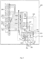
- FIG. 2 illustrates a first embodiment of a battery system 300 according to the invention.
- the battery system 300 comprises a plurality of battery modules which are connected in series.
- all battery modules comprise a plurality of battery cells 10, which are exemplarily connected in series.
- the battery cells 10 of the battery modules can also be connected in parallel or in parallel and in series.
- each battery module comprises a first and a second terminal respectively. Of the plurality of battery cells 10, only three battery cells 10 per battery module are shown for the sake of a better understanding.
- the battery system 300 shown in figure 2 comprises a plurality of bus bars, interconnecting the terminals of the battery modules respectively.
- a first bus bar 100 is electrically connecting the first terminal 11-1 of the first battery module 1 with the terminal of another battery module 7.
- the first bus bar 100 can also be used to connect the first terminal 11-1 of the first battery module 1 with a another potential (not shown) of the battery system 300.
- the battery system 300 comprises a second bus bar 200, electrically connecting the second terminal 11-2 of the first battery module 1 with the first terminal 12-1 of the second battery module 2.
- the other battery modules are interconnected via bus bars respectively.
- the battery system 300 further comprises a Cell Supervision Circuit Unit 50 with a plurality of input channels CH0-CH12, wherein the first and second terminal 11-1, 11-2, 12-1, 12-2 of the first and second battery module 1, 2 are connected to one of the plurality of input channels CH0-CH12 respectively, wherein the first terminal 11-1 of the first battery module 1 is electrically connected to a GND-input channel CH0. Furthermore, each terminal of the battery cells 10 of the first and second battery module 1, 2 is electrically connected to an input channel CH0-CH12 of the Cell Supervision Circuit Unit 50.
- the Cell Supervision Circuit Unit 50 exemplarily is realized as a 12-Channel Analog-Frontend (AFE)-Chip which is adapted to measure the voltages at the points of connection to the battery modules.
- the Cell Supervision Circuit Unit 50 is not adapted to directly measure the voltage dropping across the second bus bar 200 electrically interconnecting the first and the second battery module 1, 2. Also the voltages dropping across the third bus bar 230 electrically interconnecting the second and the third battery module 2, 3 and across the fourth bus bar 240 electrically interconnecting the third and the fourth battery module 3, 5 cannot simply be measured using the Cell Supervision Circuit Unit 50 for the reasons mentioned further above.
- the Cell Supervision Circuit Unit 50 is adapted to measure the voltage drop U 1sBB across the first bus bar 100, which is performed using a level shifter circuit 120 that is electrically connected to the Cell Supervision Circuit Unit 50 and to the first battery module 1 and which will be described further below.
- the battery system 300 further comprises an electronic circuit 150 adapted to calculate the voltage drop U 2ndBB across the second bus bar 200, using the measured voltage drop across the first bus bar 100. Furthermore, in this embodiment, the electronic circuit 150 is also adapted to calculate the voltage drops across the other bus bars 230, 240 of the battery system 300, especially the voltage drops U 3rdBB , U 4thBB across the third and fourth bus bar 230, 240 of the battery system 300.
- the aforementioned voltage drops U 2ndBB , U 3rdBB , U 4thBB are calculated as a function of the measured voltage drop U 1stBB across the first bus bar 100 and of the geometrical length I BB of the bus bars 100, 200, 230, 240 respectively, as the width and the height of the bus bars 100, 200, 230, 240 of the battery system 300 in this embodiment are identical. Furthermore, in this embodiment, all bus bars 100, 200, 230, 240 are made of copper.
- the electronic circuit 150 can also be adapted to calculate the aforementioned voltage drops U 2ndBB , U 3rdBB , U 4thBB , further considering different width, heights or materials of the different bus bars 100, 200, 230, 240.
- the electronic circuit 150 in this embodiment is integrated within the Cell Supervision Circuit Unit 50. However, it can also be a component that is separate from the Cell Supervision Circuit Unit 50 and/or integrated within another component of the battery system 300, for example within a battery management unit or a battery management system of the battery system 300, or in a separate internal or external processing unit of the battery system 300.
- U 1sBB is the measured voltage drop across the first bus bar 100
- I 2ndBB is the geometrical length of the second bus bar 200
- I 1stBB is the geometrical length of the first bus bar 100.
- the electronic circuit 150 is adapted to calculate the voltage drops U 3rdBB , U 4thBB in the same manner, using the same formula.
- the battery system 300 further comprises a level shifter circuit 120 electrically connected to the Cell Supervision Circuit Unit 50 and to the first battery module 1, 2.
- the level shifter circuit 120 allows for the measurement of negative voltages and comprises an inverting amplifier 121, wherein the inverting amplifier 121 comprises an operational amplifier 125, the operational amplifier 125 comprising an inverting input terminal 125-1, a non-inverting input terminal 125-2 and an output terminal 128.
- the output terminal 128 of the operational amplifier 125 is electrically connected to a general purpose input/output terminal GPIO of the Cell Supervision Circuit Unit 50.
- the inverting input terminal 125-1 of the operational amplifier 125 is electrically connected to the first bus bar 100, in more detail to a fraction of the first bus bar 100 that is connected to the terminal of the another battery module 7.
- the general purpose input/output terminal GPIO of the Cell Supervision Circuit Unit 50 the output terminal 128 of the operational amplifier 125 is connected to is adapted to measure the voltage at the output terminal 128 down to a predefined negative boundary, which in this embodiment exemplarily is equal to -1,5V.
- a first resistor R 1 is connected in series to the inverting input terminal 125-1.
- the non-inverting input terminal 125-2 of the operational amplifier 125 is electrically connected to a reference output terminal REF_OUT of the Cell Supervision Circuit Unit 50.
- a second resistor R 2 is arranged in the electrical path electrically interconnecting the non-inverting input terminal 125-2 of the operational amplifier 125 with the reference output terminal REF_OUT of the Cell Supervision Circuit Unit 50.
- the reference output terminal REF_OUT of the Cell Supervision Circuit Unit 50 in this embodiment is adapted to output a reference voltage for the level shifter circuit 120.
- the operational amplifier 125 comprises a feedback circuit, comprising an electrical path 129 that is connected to the output terminal 128 of the operational amplifier 125 and to the inverting input terminal 125-1 of the operational amplifier 125.
- the electrical path 129 of the feedback circuit comprises a third and fourth resistor R 3 , R 4 connected in series.
- a fifth resistor R 5 is arranged within an electrical path electrically interconnecting the non-inverting input terminal 125-2 of the operational amplifier 125 with the ground potential 4 of the battery system 300.
- the resistors R 1 , R 2 , R 3 , R 4 and R 5 exemplarily have the same value of 10k ⁇ . However, they also can have any other value respectively and differ from one another. Thus, in another embodiment, R 1 , R 2 , R 3 , R 4 and R 5 may have different values.
- the reference output terminal REF_OUT of the Cell Supervision Circuit Unit 50 in this embodiment is electrically connected to the first terminal of a switching element 60, the second terminal of the switching element 60 being electrically connected to the inverting input terminal 125-1 of the operational amplifier 125.
- the switching element 60 is exemplarily realized as a PMOS-transistor, however, it also can be realized as any other kind of switching element, for example as another FET, as a bipolar transistor or as another kind of switching means.
- the Gate-Terminal of the PMOS-transistor in this embodiment exemplarily is electrically connected to another general purpose input/output terminal GPIO of the Cell Supervision Circuit Unit 50, adapted to provide the Gate-Terminal of the PMOS-transistor with a voltage allowing for the transfer of the switching element 60/the PMOS-transistor into a conductive state.
- the further resistor R6 also can have any other value or be omitted, just as the resistors R 1 , R 2 , R 3 , R 4 and R 5 -
- the reference output terminal REF_OUT of the Cell Supervision Circuit Unit 50 in this embodiment is adapted to provide for a reference voltage for the non-inverting input terminal 125-2 of the operational amplifier 125.
- the reference voltage provided to the non-inverting input terminal 125-2 of the operational amplifier 125 exemplarily has a value of 1,5V.
- the reference output terminal REF_OUT of the Cell Supervision Circuit Unit 50 in this embodiment is adapted to provide for a test voltage which will be described further hereinafter.
- the operational amplifier 125 comprises a first and a second power supply input terminal 126, 127, wherein the first power supply input terminal 126 is electrically connected to the ground potential 4 of the battery system 300 and wherein the second power supply input terminal 127 is electrically connected to the Cell Supervision Circuit Unit 50, in more detail to a power supply output of the Cell Supervision Circuit Unit 50, denoted VREG, which is adapted to supply the second power supply input terminal 127 with a voltage of in this embodiment exemplarily 5V.
- VREG power supply output of the Cell Supervision Circuit Unit 50
- the resistors R1 to R5 are equal to the resistors R 1 , R 2 , R 3 , R 4 and R 5 described further above.
- the absolute value of this gain decreases due to different aspects.
- These aspects among others comprise an error caused by an offset of the operational amplifier 125 and the accuracy of the reference voltage provided by the reference output terminal REF_OUT of the Cell Supervision Circuit Unit 50. While the reference voltage directly provided at the reference output terminal REF_OUT of the Cell Supervision Circuit Unit 50 is equal to 2V, the reference voltage U REF finally supplied to the non-inverting input terminal 125-2 is equal to 1.5V.
- the PMOS-transistor in order to reach a required Automotive Safety Integrity Level (ASIL), can be switched on via the another general purpose input/output terminal GPIO of the Cell Supervision Circuit Unit 50, allowing for a diagnoses of the level shifter circuit 120, providing the inverting input terminal 125-1 of the operational amplifier 125 with an additional voltage.
- the operational amplifier 125 is chosen to be the TSV631. However, also any other suitable operational amplifier 125 can be used.
- the accuracy of the resistors R 1 to R 6 is 0.1%, having a 10ppm temperature coefficient, the presented circuit is sufficient to get the required accuracy of the bus bar measurement.
- the arrow indicates an arrangement of input filters and of a balancing circuit which is not shown in figure 2 for the sake of a better understanding.
- a balancing circuit and input filters which in this embodiment are realized as low pass filters, are arranged in between the input channels CH0 to CH12 of the Cell Supervision Circuit Unit 50 and the battery modules of the battery system.
- the linearity of the calculated inductance can be changed/transferred to an insignificant value.
- the inductive, not scalable part of the impedance is suppressed to an insignificant value.
- the voltage drop is linearly scalable and the incorrectly measured cell voltage can be corrected.
- the voltages of the battery modules and battery cells 10 have to be measured synchronously via the input channels CH0 to CH12 of the Cell Supervision Circuit Unit 50. If the time constant of the aforementioned input filters is high, then a small shift between the measurements does not influence the result.
- a diagram is shown illustrating the voltage drop across the first bus bar 100 in dependence of the length of the first bus bar 100, with and without low-pass filtering.
- the ordinate of the diagram of figure 3 shows the voltage drop across the first bus bar 100 in mV.
- the abscissa shows the length of the respective first bus bar 100 in cm.
- the dotted line in the diagram shows the voltage drop across the first bus bar 100 without that a low-pass-filtering is applied to the measured values.
- the continuous line in the diagram of figure 3 shows the voltage drop across the first bus bar 100 with a low-pass-filtering that is applied to the measurement.
- Figure 4 illustrates a voltage drop calculated from a measured current by the electronic circuit 150 of the embodiment of a battery system 300 shown in figure 2 .
- figure 4 shows two diagrams.
- the upper diagram shown in figure 4 illustrates the current in ampere measurable over time in seconds at the output 128 of the operational amplifier 120 of the battery system 300 shown in figure 2 .
- the lower diagram shown in figure 4 illustrates the voltage drop across the second bus bar 200 in mV over time in seconds, using a realistic drive cycle, the voltage drop being calculated/simulated from the aforementioned measured current as shown in the upper diagram.
Landscapes
- Physics & Mathematics (AREA)
- General Physics & Mathematics (AREA)
- Secondary Cells (AREA)
- Measurement Of Current Or Voltage (AREA)
Abstract
Description
- The present invention relates to a battery system which comprises a first and a second battery module, comprising at least one battery cell and a first and a second terminal respectively. The battery system further comprises a first bus bar, electrically connecting the first terminal of the first battery module with the terminal of another battery module and/or with a potential of the battery system. Moreover, the battery system comprises a second bus bar, electrically connecting the second terminal of the first battery module with the first terminal of the second battery module. Furthermore, the battery system comprises a Cell Supervision Circuit Unit with a plurality of input channels, wherein the first and second terminal of the first and second battery module are connected to one of the plurality of input channels respectively, the first terminal of the first battery module being connected to a GND-input channel.
- A rechargeable or secondary battery system differs from a primary battery system in that it can be repeatedly charged and discharged, while the latter provides only an irreversible conversion of chemical to electrical energy. Low-capacity rechargeable battery systems are used as power supply for small electronic devices, such as cellular phones, notebook computers and camcorders, while high-capacity rechargeable battery systems are used as the power supply for hybrid vehicles and the like.
- Usually, battery systems comprise a plurality of battery modules, wherein the battery modules comprise a plurality of battery cells. The battery cells of a battery module are controlled and supervised with regard to a plurality of different parameters, as for example their respective State of Charge (SoC), temperature and output voltage via so called Cell Supervision Circuit Units (CSC). Such Cell Supervision Circuits or Cell Supervision Circuit Units often are realized as Analog-Front-End (AFE) chips and/or as printed circuit boards (PCB) that are available having 6, 12 or 18 input channels respectively. In the state of the art, one Cell Supervision Circuit Unit is allocated to one battery module respectively.
- However, as many different electronic components come to use within a Cell Supervision Circuit Unit (CSC), such an allocation is cost intensive and inefficient regarding the overall power consumption of the battery system.
- A
battery system 300 of the state of the art is shown infigure 1 . Thebattery system 300 comprises six battery modules, each battery module comprising a plurality ofbattery cells 10 and an own CellSupervision Circuit Unit 50 respectively. The input channels of the CellSupervision Circuit Units 50 of the battery modules are electrically connected to thebattery cells 10 of the respective corresponding battery module. Furthermore, thebattery system 300 shown infigure 1 exemplarily comprises abattery management unit 255 which is connected to the first of thebattery modules 1 via aconnector 256 of thebattery management unit 255. Via afirst bus bar 100, the first terminal 11-1 of thefirst battery module 1 is electrically connected to a predefined potential 4 which in this example is exemplarily equal to the potential of a plus pole of thebattery system 300. Furthermore, via asecond bus bar 200, the second terminal 11-2 of thefirst battery module 1 is electrically connected to the first terminal 12-1 of thesecond battery module 2 of the six battery modules. In this example, the first and thesecond bus bars - Via further bus bars, the remaining battery modules are electrically interconnected in series.
- One or more of the drawbacks of the prior art could be avoided or at least reduced by means of the present invention. In particular, a battery system is provided. The battery system comprises a first and a second battery module, comprising at least one battery cell and a first and a second terminal respectively. Furthermore, the battery system comprises a first bus bar, electrically connecting the first terminal of the first battery module with the terminal of another battery module and/or with a potential of the battery system. Moreover, the battery system comprises a second bus bar, electrically connecting the second terminal of the first battery module with the first terminal of the second battery module. The battery system further comprises a Cell Supervision Circuit Unit with a plurality of input channels, wherein the first and second terminal of the first and second battery module are connected to one of the plurality of input channels respectively, the first terminal of the first battery module being connected to a GND-input channel. The Cell Supervision Circuit Unit is adapted to measure the voltage drop across the first bus bar.
- With such a battery system, it is possible to allocate one single Cell Supervision Circuit Unit to two or more than two battery modules, as the measurement of the voltage drop across the first bus bar allows for the calculation/estimation of the voltage that drops across the other bus bars of the battery system respectively, thus allowing for one Cell Supervision Circuit Unit to control and supervise the battery cells of multiple different battery modules. The voltage drop across the first bus bar can easily be measured, as the first bus bar is connected to the GND-input channel of the Cell Supervision Circuit Unit. The voltage drop across the other bus bars of the battery system cannot simply be measured, as these bus bars are not on the ground potential of the Cell Supervision Circuit Unit. Therefore, if the Cell Supervision Circuit Unit was used to control and supervise the battery cells also of the second battery module, this control/supervision would be performed erroneously, as the voltage drop across the second bus bar would not be considered by the Cell Supervision Circuit Unit. It is not possible to simply measure the voltages that drop across the second bus bar with one separate channel of the Cell Supervision Circuit Unit, as it is not possible to measure negative voltages with the same. However, when the voltage drop across the second and the further bus bars of a battery system is calculated, the calculated voltages can be taken into account by a Cell Supervision Circuit Unit, thus allowing for the same to control and supervise a plurality of battery modules - and the battery cells thereof - interconnected via bus bars. Expressed in other words, the invention allows for the usage of a shared Cell Supervision Circuit Unit for a plurality of battery modules, interconnected via multiple connectors/bus bars.
- Preferably, a bus bar is a conductive strip or bar that conducts electricity within a battery system, electrically interconnecting the terminals of battery modules and/or of battery cells and/or of electrical apparatuses and components. Preferably, the bus bar is a conductive metallic strip or bar.
- Preferably, the GND-input channel is a ground input channel or an input channel for a ground potential.
- Preferably, a Cell Supervision Circuit Unit is equal to a full Cell Supervision Circuit.
- Preferably, the potential of the battery system is equal to a ground potential, to the potential of a plus pole or to the potential of a minus pole of the battery system. Furthermore preferred, the potential of the battery system is substantially equal to a ground potential, to the potential of a plus pole or to the potential of a minus pole of the battery system.
- Preferably, a terminal of a battery module is formed by a terminal of a battery cell of the respective battery module. Especially preferred, the first terminal of the first battery module is formed by a terminal of a battery cell of the first battery module.
- Preferably, the Cell Supervision Circuit Unit is realized as a chip or a chipset. Preferably, the Cell Supervision Circuit Unit has six input channels. Even more preferred, the Cell Supervision Circuit Unit has 12 input channels. In such an embodiment, the maximum number of cells that can be handled by a single Cell Supervision Circuit Unit is 12. Furthermore preferred, the Cell Supervision Circuit Unit has 18 input channels. In many applications - as for example in electric vehicle (EV) applications - the number of serial connected battery cells per battery module is low, which is due to a high number of parallel battery cell connections. Therefore it is possible to use a single Cell Supervision Circuit Unit for more than one battery module.
- Preferably, the first terminal of the first battery module is connected to a GND-input channel of the Cell Supervision Circuit Unit.
- Preferably, the battery system further comprises an electronic circuit, adapted to calculate the voltage drop across the second bus bar, using the measured voltage drop across the first bus bar. In such an embodiment, it is possible to precisely calculate the voltage dropping across the bus bars coming to use within the battery system. This allows for a significant reduction of costs. Furthermore, when compared to an approach that neglects the voltage drop over the bus bars between the battery modules, the accuracy is increased. When compared to an approach in which the voltage drop over the further bus bars is measured with an additional input channel of the Cell Supervision Circuit Unit, there is no risk of a negative voltage being supplied to an input of a battery management system chip which may damage the same through an overvoltage. Thus, the invention allows for the usage of a single Cell Supervision Circuit Unit to supervise/control multiple battery modules of the battery system and thus to significantly decrease the number of Cell Supervision Circuit Units coming to use within the battery system. Therefore, the costs of production and the power consumption of the battery system are significantly decreased and the energy efficiency of the battery system is significantly increased. When the voltage drops across the bus bars are known, the voltages of the different cells of the battery modules can be measured and adjusted accordingly by the Cell Supervision Circuit Unit coming to use.
- In a preferred embodiment, the electronic circuit is adapted to calculate the voltage drop across the second bus bar as a function of the measured voltage drop across the first bus bar and of at least one geometrical parameter of the second bus bar. In a series connection of battery modules, the same current flows through every bus bar. Therefore, the voltage drop across a bus bar should substantially be the same for same dimensions - apart from negligible influence of the temperature. If a bus bar is twice as long as the another bus bar - and the other dimensions as width and height of the bus bars are the same - the voltage dropping across this bus bar is also doubled. Due to this reason the voltage drop can be calculated for different lengths of bus bars, when the voltage drop of one bus bar is known.
- Preferably, the width and height of the first and the second bus bar are identical or substantially identical. Furthermore preferred, the voltage drop across the second bus bar is calculated using the formula:

- Preferably, the at least one geometrical parameter is chosen out of a group of parameters, the group of parameters comprising the length of the second bus bar, the width of the second bus bar and the height of the second bus bar. In such an embodiment, the calculation of the voltage drops across the other bus bars can be performed in a highly accurate manner.
- In a preferred embodiment, the electronic circuit is adapted to calculate the voltage drop across the second bus bar as a function of the measured voltage drop across the first bus bar and of at least one parameter of the second bus bar. Preferably, the at least one parameter is the material of the second bus bar.
- Preferably, the electronic circuit is adapted to consider and/or calculate the inductivity of the bus bar in order to calculate the voltage dropping across the second bus bar. Preferably, the electronic circuit is adapted to consider and/or calculate the inductivity of the second bus bar according to the formula:

- Preferably, the electronic circuit is further adapted to consider and/or calculate the ohmic resistance of the second bus bar in order to calculate the voltage dropping across the second bus bar, wherein the cross section, the length and/or the material of the second bus bar is considered.
- Preferably, the electronic circuit is adapted to calculate the ohmic resistance R of a bus bar of a predefined material M according to the following formula:

- Preferably, the first and second bus bars comprise copper. Preferably, the electronic circuit is adapted to calculate the ohmic resistance RCU of a copper bus bar according to the following formula:

- Preferably, the ratio IBB/R is constant for all the bus bars of the battery system.
- Preferably, at least one input filter, especially a low-pass filter is used to reduce the measured voltage drop due to the inductance of the bus bar. As can be derived from the aforementioned formulas, the voltage drop across the bus bars is not linearly scalable due to the length of the bus bars respectively. However, with the aforementioned input filters, the linearity of the calculated inductance can be changed/transferred to an insignificant value.
- Expressed in other words, when a low pass filter is used, the inductive, not scalable part of the impedance is suppressed to an insignificant value. By using only the scalable ohmic part of the impedance, the voltage drop is linearly scalable and the incorrectly measured cell voltage can be corrected.
- In a preferred embodiment, the electronic circuit is integrated within the Cell Supervision Circuit Unit. In such an embodiment, the battery system is even more compact, as the electronic circuit which is allowing for the omittance of a plurality of Cell Supervision Circuit Units is integrated within the one Cell Supervision Circuit Unit that is maintained within the battery system and thus does not require a lot of additional space.
- Preferably, the electronic circuit comprises a processing unit. Such a processing unit allows for quick and accurate calculations. Preferably, the processing unit is realized as a microcontroller or a microprocessor.
- In a preferred embodiment, the battery system further comprises a level shifter circuit electrically connected to the Cell Supervision Circuit Unit and/or to the first and/or second battery module. In such an embodiment, the level shifter circuit can be used to measure positive and negative voltages, preventing negative voltages from directly being supplied to the input channels of the Cell Supervision Circuit Unit and thus from destroying the Cell Supervision Circuit Unit.
- Preferably, the level shifter circuit is a part of the electronic circuit. Furthermore preferred, the level shifter circuit is a part of the Cell Supervision Circuit Unit.
- In a preferred embodiment, the level shifter circuit comprises an inverting amplifier, wherein the inverting amplifier comprises an operational amplifier, the operational amplifier comprising an inverting input terminal, a non-inverting input terminal and an output terminal. Such an inverting amplifier with an operational amplifier is reliable, provides for a high gain and has a high input resistance and a low output resistance. Preferably, the value of the sum of the resistances within the feedback circuit of the inverting amplifier is twice as high as the value of the sum of the resistances arranged in series to the inverting input terminal of the inverting amplifier, providing for a gain A of A = -2. Preferably, the value of the sum of the resistances within the feedback circuit of the inverting amplifier is 20kΩ, wherein the value of the sum of the resistances arranged in series to the inverting input terminal of the inverting amplifier is 10kΩ.
- Preferably, the output terminal of the operational amplifier is electrically connected to a general purpose input/output terminal of the Cell Supervision Circuit Unit. In such an embodiment, the measurement of the voltage drop across the first bus bar can easily be performed via the Cell Supervision Circuit Unit. Furthermore, embodiments of the invention can be carried out in which only the one single general purpose input/output terminal of the Cell Supervision Circuit Unit (GPIO) is used to measure the voltage drop across the first bus bar, thus allowing for the realization of a compact battery system.
- In a preferred embodiment, the inverting input terminal of the operational amplifier is electrically connected to the first bus bar. Preferably, the inverting input terminal of the operational amplifier is electrically connected to a fraction of the first bus bar that is on an end of the first bus bar opposing the fraction of the first bus bar that is in contact with the first terminal of the first battery module. In such an embodiment, the voltage drop across the whole first bus bar is measured.
- In a preferred embodiment, the non-inverting input terminal of the operational amplifier is electrically connected to a reference output terminal of the Cell Supervision Circuit Unit. In such an embodiment, the reference output voltage is also provided by the Cell Supervision Circuit Unit and thus does not need to be provided by an external component. This allows for a more compact design of the battery system and enables a precise measurement of the voltage drop across the first bus bar.
- Preferably, the reference output terminal of the Cell Supervision Circuit Unit is electrically connected to the first terminal of a switching element, the second terminal of the switching element being electrically connected to the inverting input terminal of the operational amplifier. The switching element is provided for diagnosis purposes in order to reach a predefined Automotive Safety Integrity Level (ASIL). The switching element can for example be switched on a test voltage of 10k/100k*3V=300mV.
- In a preferred embodiment, the switching element is a field effect transistor. Such field effect transistors have lower losses than for example bipolar transistors and allow for a quick switching of currents.
- Especially preferred, the switching element is a PMOS transistor. PMOS transistors can be realized as highly integrated elements that have small dimensions but nevertheless allow for a reliable switching of currents.
- Preferably, the operational amplifier comprises a first and a second power supply input terminal, wherein the first power supply input terminal is electrically connected to the ground potential of the battery system and/or wherein the second power supply input terminal is electrically connected to the Cell Supervision Circuit Unit. In such an embodiment, no further component needs to be provided for the supply of power to the power supply input terminals, allowing for a compact realization of the battery system.
- Preferably, an inaccuracy of an offset voltage and of a reference voltage of the operational amplifier is compensated by zerogoing, when a current through the bus bars is equal to zero. When the current through a bus bar is equal to zero, there should also be a voltage drop measurable across the bus bars which is equal to zero. This offset can be calibrated when there is no current drawn out of the battery system.
- According to another aspect of the present invention, a vehicle including a battery system as defined above is provided.
- Further aspects of the present invention could be learned from the dependent claims or the following description.
- Features will become apparent to those of ordinary skill in the art by describing in detail exemplary embodiments with reference to the attached drawings in which:
- Fig. 1
- illustrates a battery system of the state of the art;
- Fig. 2
- illustrates a battery system according to an embodiment of the invention;
- Fig. 3
- illustrates a diagram showing the voltage drop across the first bus bar in dependence of the length of the first bus bar, with and without low-pass filtering, and
- Fig. 4
- illustrates a voltage drop calculated from a measured current by the electronic circuit of the embodiment of a battery system as shown in
figure 2 . - Reference will now be made in detail to embodiments, examples of which are illustrated in the accompanying drawings. Effects and features of the exemplary embodiments will be described with reference to the accompanying drawings. In the drawings, like reference numerals denote like elements, and redundant descriptions are omitted. As used herein, the term "and/or" includes any and all combinations of one or more of the associated listed items. Further, the use of "may" when describing embodiments of the present invention refers to "one or more embodiments of the present invention."
- It will be understood that although the terms "first" and "second" are used to describe various elements, these elements should not be limited by these terms. These terms are only used to distinguish one element from another element. For example, a first element may be named a second element and, similarly, a second element may be named a first element, without departing from the scope of the present invention.
- In the following description of embodiments of the present invention, the terms of a singular form may include plural forms unless the context clearly indicates otherwise.
- The present invention, may be embodied in various different forms, and should not be construed as being limited to only the illustrated embodiments herein. Rather, these embodiments are provided as examples so that this disclosure will be thorough and complete, and will fully convey the aspects and features of the present invention to those skilled in the art. Accordingly, elements and techniques that are not necessary to those having ordinary skill in the art for a complete understanding of the aspects and features of the present invention may not be described.
- It will be understood that, although the terms "first," "second," "third," etc., may be used herein to describe various elements and/or components, these elements and/or components should not be limited by these terms. These terms are used to distinguish one element and/or component from another element and/or component. Thus, a first element and/or component described below could be termed a second element and/or component, without departing from the scope of the present invention.
- It will be understood that when an element or component is referred to as being "on," "connected to," or "coupled to" another element or component, it can be directly on, connected to, or coupled to the other element or component, or one or more intervening elements or components may be present. In addition, it will also be understood that when an element or component is referred to as being "between" two elements or components, it can be the only element or component between the two elements or components, or one or more intervening elements or components may also be present.
- The terminology used herein is for the purpose of describing particular embodiments only and is not intended to be limiting of the present invention. As used herein, the singular forms "a," "an," and "the" are intended to include the plural forms as well, unless the context clearly indicates otherwise. It will be further understood that the terms "comprises," "comprising," "includes," and "including," when used in this specification, specify the presence of the stated features, integers, operations, elements, and/or components, but do not preclude the presence or addition of one or more other features, integers, operations, elements, components, and/or groups thereof. As used herein, the term "and/or" includes any and all combinations of one or more of the associated listed items. Expressions such as "at least one of," when preceding a list of elements, modify the entire list of elements and do not modify the individual elements of the list.
- As used herein, the term "substantially," "about," and similar terms are used as terms of approximation and not as terms of degree, and are intended to account for the inherent deviations in measured or calculated values that would be recognized by those of ordinary skill in the art. Further, if the term "substantially" is used in combination with a feature that could be expressed using a numeric value, the term "substantially" denotes a range of +/- 5% of the value centered on the value.
-
Figure 2 illustrates a first embodiment of abattery system 300 according to the invention. Thebattery system 300 comprises a plurality of battery modules which are connected in series. In the following, for the sake of a better understanding, the invention will be described mainly referring to a first, a second and athird battery module battery cells 10, which are exemplarily connected in series. However, in other embodiments, thebattery cells 10 of the battery modules can also be connected in parallel or in parallel and in series. Furthermore, each battery module comprises a first and a second terminal respectively. Of the plurality ofbattery cells 10, only threebattery cells 10 per battery module are shown for the sake of a better understanding. - Moreover, the
battery system 300 shown infigure 2 comprises a plurality of bus bars, interconnecting the terminals of the battery modules respectively. Afirst bus bar 100 is electrically connecting the first terminal 11-1 of thefirst battery module 1 with the terminal of another battery module 7. However, as shown infigure 1 , thefirst bus bar 100 can also be used to connect the first terminal 11-1 of thefirst battery module 1 with a another potential (not shown) of thebattery system 300. Furthermore, thebattery system 300 comprises asecond bus bar 200, electrically connecting the second terminal 11-2 of thefirst battery module 1 with the first terminal 12-1 of thesecond battery module 2. In this embodiment, also the other battery modules are interconnected via bus bars respectively. Thebattery system 300 further comprises a CellSupervision Circuit Unit 50 with a plurality of input channels CH0-CH12, wherein the first and second terminal 11-1, 11-2, 12-1, 12-2 of the first andsecond battery module first battery module 1 is electrically connected to a GND-input channel CH0. Furthermore, each terminal of thebattery cells 10 of the first andsecond battery module Supervision Circuit Unit 50. - In this embodiment, the Cell
Supervision Circuit Unit 50 exemplarily is realized as a 12-Channel Analog-Frontend (AFE)-Chip which is adapted to measure the voltages at the points of connection to the battery modules. The CellSupervision Circuit Unit 50 is not adapted to directly measure the voltage dropping across thesecond bus bar 200 electrically interconnecting the first and thesecond battery module third battery module 2, 3 and across thefourth bus bar 240 electrically interconnecting the third and thefourth battery module 3, 5 cannot simply be measured using the CellSupervision Circuit Unit 50 for the reasons mentioned further above. Infigure 2 , this is indicated via a lightning symbol in between the respective channels CH3, CH4 and between CH6 and CH7 and between CH 9 and CH10 of the CellSupervision Circuit Unit 50 respectively. However, the CellSupervision Circuit Unit 50 is adapted to measure the voltage drop U1sBB across thefirst bus bar 100, which is performed using alevel shifter circuit 120 that is electrically connected to the CellSupervision Circuit Unit 50 and to thefirst battery module 1 and which will be described further below. - In this embodiment, the
battery system 300 further comprises anelectronic circuit 150 adapted to calculate the voltage drop U2ndBB across thesecond bus bar 200, using the measured voltage drop across thefirst bus bar 100. Furthermore, in this embodiment, theelectronic circuit 150 is also adapted to calculate the voltage drops across theother bus bars 230, 240 of thebattery system 300, especially the voltage drops U3rdBB, U4thBB across the third andfourth bus bar 230, 240 of thebattery system 300. In this embodiment, the aforementioned voltage drops U2ndBB, U3rdBB, U4thBB are calculated as a function of the measured voltage drop U1stBB across thefirst bus bar 100 and of the geometrical length IBB of the bus bars 100, 200, 230, 240 respectively, as the width and the height of the bus bars 100, 200, 230, 240 of thebattery system 300 in this embodiment are identical. Furthermore, in this embodiment, allbus bars electronic circuit 150 can also be adapted to calculate the aforementioned voltage drops U2ndBB, U3rdBB, U4thBB, further considering different width, heights or materials of thedifferent bus bars electronic circuit 150 in this embodiment is integrated within the CellSupervision Circuit Unit 50. However, it can also be a component that is separate from the CellSupervision Circuit Unit 50 and/or integrated within another component of thebattery system 300, for example within a battery management unit or a battery management system of thebattery system 300, or in a separate internal or external processing unit of thebattery system 300. - In this embodiment, the
electronic circuit 150 is adapted to calculate the voltage dropping across thesecond bus bar 200 according to the formula:
second bus bar 200. U1sBB is the measured voltage drop across thefirst bus bar 100, I2ndBB is the geometrical length of thesecond bus bar 200 and I1stBB is the geometrical length of thefirst bus bar 100. In this embodiment, the measured voltage drop U1sBB across thefirst bus bar 100 exemplarily is U1sBB = -13mV, wherein the length of thefirst bus bar 100 is I1stBB = 135mm. The length of thesecond bus bar 200 is I2ndBB = 405mm. As allbus bars electronic circuit 150 calculates:
- Furthermore, the
electronic circuit 150 is adapted to calculate the voltage drops U3rdBB, U4thBB in the same manner, using the same formula. - As already mentioned, the
battery system 300 further comprises alevel shifter circuit 120 electrically connected to the CellSupervision Circuit Unit 50 and to thefirst battery module level shifter circuit 120 allows for the measurement of negative voltages and comprises an invertingamplifier 121, wherein the invertingamplifier 121 comprises anoperational amplifier 125, theoperational amplifier 125 comprising an inverting input terminal 125-1, a non-inverting input terminal 125-2 and anoutput terminal 128. In this embodiment, theoutput terminal 128 of theoperational amplifier 125 is electrically connected to a general purpose input/output terminal GPIO of the CellSupervision Circuit Unit 50. The inverting input terminal 125-1 of theoperational amplifier 125 is electrically connected to thefirst bus bar 100, in more detail to a fraction of thefirst bus bar 100 that is connected to the terminal of the another battery module 7. The general purpose input/output terminal GPIO of the CellSupervision Circuit Unit 50 theoutput terminal 128 of theoperational amplifier 125 is connected to is adapted to measure the voltage at theoutput terminal 128 down to a predefined negative boundary, which in this embodiment exemplarily is equal to -1,5V. - A first resistor R1 is connected in series to the inverting input terminal 125-1. The non-inverting input terminal 125-2 of the
operational amplifier 125 is electrically connected to a reference output terminal REF_OUT of the CellSupervision Circuit Unit 50. A second resistor R2 is arranged in the electrical path electrically interconnecting the non-inverting input terminal 125-2 of theoperational amplifier 125 with the reference output terminal REF_OUT of the CellSupervision Circuit Unit 50. The reference output terminal REF_OUT of the CellSupervision Circuit Unit 50 in this embodiment is adapted to output a reference voltage for thelevel shifter circuit 120. Moreover, theoperational amplifier 125 comprises a feedback circuit, comprising anelectrical path 129 that is connected to theoutput terminal 128 of theoperational amplifier 125 and to the inverting input terminal 125-1 of theoperational amplifier 125. Theelectrical path 129 of the feedback circuit comprises a third and fourth resistor R3, R4 connected in series. A fifth resistor R5 is arranged within an electrical path electrically interconnecting the non-inverting input terminal 125-2 of theoperational amplifier 125 with the ground potential 4 of thebattery system 300. In this embodiment, the resistors R1, R2, R3, R4 and R5 exemplarily have the same value of 10kΩ. However, they also can have any other value respectively and differ from one another. Thus, in another embodiment, R1, R2, R3, R4 and R5 may have different values. - The reference output terminal REF_OUT of the Cell
Supervision Circuit Unit 50 in this embodiment is electrically connected to the first terminal of a switching element 60, the second terminal of the switching element 60 being electrically connected to the inverting input terminal 125-1 of theoperational amplifier 125. The switching element 60 is exemplarily realized as a PMOS-transistor, however, it also can be realized as any other kind of switching element, for example as another FET, as a bipolar transistor or as another kind of switching means. The Gate-Terminal of the PMOS-transistor in this embodiment exemplarily is electrically connected to another general purpose input/output terminal GPIO of the CellSupervision Circuit Unit 50, adapted to provide the Gate-Terminal of the PMOS-transistor with a voltage allowing for the transfer of the switching element 60/the PMOS-transistor into a conductive state. In this embodiment, the switching element 60 is connected in series to a further resistor R6 which has a value of exemplarily R6 = 100kΩ. However, the further resistor R6 also can have any other value or be omitted, just as the resistors R1, R2, R3, R4 and R5-The reference output terminal REF_OUT of the CellSupervision Circuit Unit 50 in this embodiment is adapted to provide for a reference voltage for the non-inverting input terminal 125-2 of theoperational amplifier 125. The reference voltage provided to the non-inverting input terminal 125-2 of theoperational amplifier 125 exemplarily has a value of 1,5V. Furthermore, the reference output terminal REF_OUT of the CellSupervision Circuit Unit 50 in this embodiment is adapted to provide for a test voltage which will be described further hereinafter. Moreover, theoperational amplifier 125 comprises a first and a second powersupply input terminal supply input terminal 126 is electrically connected to the ground potential 4 of thebattery system 300 and wherein the second powersupply input terminal 127 is electrically connected to the CellSupervision Circuit Unit 50, in more detail to a power supply output of the CellSupervision Circuit Unit 50, denoted VREG, which is adapted to supply the second powersupply input terminal 127 with a voltage of in this embodiment exemplarily 5V. - The output voltage Uout at the
output terminal 128 of thelevel shifter circuit 120 in this embodiment can be calculated according to the equation:
operational amplifier 125 and wherein UREF is the reference voltage provided to the non-inverting input terminal 125-2 of theoperational amplifier 125. The resistors R1 to R5 are equal to the resistors R1, R2, R3, R4 and R5 described further above. - In this equation, the term

operational amplifier 125, wherein the gain A of thelevel shifter circuit 120 in this embodiment exemplarily is equal to
- As mentioned before, the resistors R1, R3 and R4 have the same value, causing the gain of the inverting
amplifier 121 and of thelevel shifter circuit 120 to be A = -2. However, the absolute value of this gain decreases due to different aspects. These aspects among others comprise an error caused by an offset of theoperational amplifier 125 and the accuracy of the reference voltage provided by the reference output terminal REF_OUT of the CellSupervision Circuit Unit 50. While the reference voltage directly provided at the reference output terminal REF_OUT of the CellSupervision Circuit Unit 50 is equal to 2V, the reference voltage UREF finally supplied to the non-inverting input terminal 125-2 is equal to 1.5V. - This means that a negative voltage down to -1.5V can be measured with the
level shifter circuit 120. If the voltage UIN at theoperational amplifier 125 is below -1.5V, for example UIN = -2V, this voltage cannot be measured anymore by thelevel shifter circuit 120, causing theoperational amplifier 125 to come into saturation. However, even in the case of such a saturation, the CellSupervision Circuit Unit 50 which in this embodiment is realized as an AFE chip (see above) is not destroyed. The switching element 60 which in this embodiment is realized as a PMOS-transistor is provided for diagnoses purposes. In more detail, in order to reach a required Automotive Safety Integrity Level (ASIL), the PMOS-transistor can be switched on via the another general purpose input/output terminal GPIO of the CellSupervision Circuit Unit 50, allowing for a diagnoses of thelevel shifter circuit 120, providing the inverting input terminal 125-1 of theoperational amplifier 125 with an additional voltage. In more detail, the PMOS-transistor allows for a test voltage of 10k/100k*3V=300mV to be supplied to the inverting input terminal 125-1 of theoperational amplifier 125. In this embodiment, theoperational amplifier 125 is chosen to be the TSV631. However, also any other suitableoperational amplifier 125 can be used. Moreover, if the accuracy of the resistors R1 to R6 is 0.1%, having a 10ppm temperature coefficient, the presented circuit is sufficient to get the required accuracy of the bus bar measurement. - In
figure 2 , the arrow indicates an arrangement of input filters and of a balancing circuit which is not shown infigure 2 for the sake of a better understanding. Expressed in other words, a balancing circuit and input filters, which in this embodiment are realized as low pass filters, are arranged in between the input channels CH0 to CH12 of the CellSupervision Circuit Unit 50 and the battery modules of the battery system. With these input filters, the linearity of the calculated inductance can be changed/transferred to an insignificant value. Thus, when a low pass filter comes to use, the inductive, not scalable part of the impedance is suppressed to an insignificant value. By using only the scalable ohmic part of the impedance the voltage drop is linearly scalable and the incorrectly measured cell voltage can be corrected. - However, depending on those input filters, the voltages of the battery modules and
battery cells 10 have to be measured synchronously via the input channels CH0 to CH12 of the CellSupervision Circuit Unit 50. If the time constant of the aforementioned input filters is high, then a small shift between the measurements does not influence the result. - In
figure 3 , a diagram is shown illustrating the voltage drop across thefirst bus bar 100 in dependence of the length of thefirst bus bar 100, with and without low-pass filtering. In more detail, the ordinate of the diagram offigure 3 shows the voltage drop across thefirst bus bar 100 in mV. The abscissa shows the length of the respectivefirst bus bar 100 in cm. The dotted line in the diagram shows the voltage drop across thefirst bus bar 100 without that a low-pass-filtering is applied to the measured values. The continuous line in the diagram offigure 3 shows the voltage drop across thefirst bus bar 100 with a low-pass-filtering that is applied to the measurement. The time constant τ of the low pass filter used is exemplarily equal to τ = 2ms. However, any other filter can come to use within a battery system that is according to the invention. -
Figure 4 illustrates a voltage drop calculated from a measured current by theelectronic circuit 150 of the embodiment of abattery system 300 shown infigure 2 . In more detail,figure 4 shows two diagrams. The upper diagram shown infigure 4 illustrates the current in ampere measurable over time in seconds at theoutput 128 of theoperational amplifier 120 of thebattery system 300 shown infigure 2 . The lower diagram shown infigure 4 illustrates the voltage drop across thesecond bus bar 200 in mV over time in seconds, using a realistic drive cycle, the voltage drop being calculated/simulated from the aforementioned measured current as shown in the upper diagram.
Claims (15)
- A battery system (300), comprising:a first and a second battery module (1, 2), comprising at least one battery cell (10) and a first and a second terminal (11-1, 11-2, 12-1, 12-2) respectively;a first bus bar (100), electrically connecting the first terminal (11-1) of the first battery module (1) with the terminal of another battery module (7) and/or with a potential (4) of the battery system (300);a second bus bar (200), electrically connecting the second terminal (11-2) of the first battery module (1) with the first terminal (12-1) of the second battery module (2);a Cell Supervision Circuit Unit (50) with a plurality of input channels (CH0-CH12), wherein the first and second terminal (11-1, 11-2, 12-1, 12-2) of the first and second battery module (1, 2) are connected to one of the plurality of input channels (CH0-CH12) respectively, the first terminal (11-1) of the first battery module (1) being connected to a GND-input channel (CHO),characterized in that,
the Cell Supervision Circuit Unit (50) is adapted to measure the voltage drop (U1stBB) across the first bus bar (100). - The battery system (300) of claim 1, further comprising an electronic circuit (150), adapted to calculate the voltage drop (U2ndBB) across the second bus bar (200), using the measured voltage drop across the first bus bar (100).
- The battery system (300) of claim 2, wherein the electronic circuit (150) is adapted to calculate the voltage drop (U2ndBB) across the second bus bar (200) as a function of the measured voltage drop (U1stBB) across the first bus bar (100) and of at least one geometrical parameter of the second bus bar (200).
- The battery system (300) of claim 3, wherein the at least one geometrical parameter is chosen out of a group of parameters, the group of parameters comprising the length (I) of the second bus bar (200), the width (w) of the second bus bar (200) and the height (h) of the second bus bar (200).
- The battery system (300) of any one of the claims 2 to 4, wherein the electronic circuit (150) is integrated within the Cell Supervision Circuit Unit (50).
- The battery system (300) of any one of the claims 2 to 5, wherein the electronic circuit (150) comprises a processing unit.
- The battery system (300) of any one of the previous claims, further comprising a level shifter circuit (120) electrically connected to the Cell Supervision Circuit Unit (50) and/or to the first and/or second battery module (1, 2).
- The battery system (300) of claim 7, wherein the level shifter circuit (120) comprises an inverting amplifier (121), wherein the inverting amplifier (121) comprises an operational amplifier (125), the operational amplifier (125) comprising an inverting input terminal (125-1), a non-inverting input terminal (125-2) and an output terminal (128).
- The battery system (300) of claim 8, wherein the output terminal (128) of the operational amplifier (125) is electrically connected to a general purpose input/output terminal (GPIO) of the Cell Supervision Circuit Unit (50).
- The battery system (300) of claim 8 or 9, wherein the inverting input terminal (125-1) of the operational amplifier (125) is electrically connected to the first bus bar (100).
- The battery system (300) of one of the claims 8 to 10, wherein the non-inverting input terminal (125-2) of the operational amplifier (125) is electrically connected to a reference output terminal (REF_OUT) of the Cell Supervision Circuit Unit (50).
- The battery system (300) of one of the claims 8 to 11, wherein the reference output terminal (REF_OUT) of the Cell Supervision Circuit Unit (50) is electrically connected to the first terminal of a switching element (60), the second terminal of the switching element (60) being electrically connected to the inverting input terminal (125-1) of the operational amplifier (125).
- The battery system (300) of claim 12, wherein the switching element (60) is a field effect transistor.
- The battery system (300) of claim 13, wherein the switching element (60) is a PMOS transistor.
- The battery system (300) of one of the claims 8 to 14, wherein the operational amplifier (125) comprises a first and a second power supply input terminal (126, 127), wherein the first power supply input terminal (126) is electrically connected to the ground potential of the battery system (300) and/or wherein the second power supply input terminal (127) is electrically connected to the Cell Supervision Circuit Unit (50).
Priority Applications (3)
| Application Number | Priority Date | Filing Date | Title |
|---|---|---|---|
| EP16200852.8A EP3327454B1 (en) | 2016-11-28 | 2016-11-28 | Battery system with a shared cell supervision circuit unit |
| PL16200852T PL3327454T3 (en) | 2016-11-28 | 2016-11-28 | Battery system with a shared cell supervision circuit unit |
| HUE16200852A HUE052482T2 (en) | 2016-11-28 | 2016-11-28 | Battery system with a shared cell supervision circuit unit |
Applications Claiming Priority (1)
| Application Number | Priority Date | Filing Date | Title |
|---|---|---|---|
| EP16200852.8A EP3327454B1 (en) | 2016-11-28 | 2016-11-28 | Battery system with a shared cell supervision circuit unit |
Publications (2)
| Publication Number | Publication Date |
|---|---|
| EP3327454A1 true EP3327454A1 (en) | 2018-05-30 |
| EP3327454B1 EP3327454B1 (en) | 2020-09-30 |
Family
ID=57406153
Family Applications (1)
| Application Number | Title | Priority Date | Filing Date |
|---|---|---|---|
| EP16200852.8A Active EP3327454B1 (en) | 2016-11-28 | 2016-11-28 | Battery system with a shared cell supervision circuit unit |
Country Status (3)
| Country | Link |
|---|---|
| EP (1) | EP3327454B1 (en) |
| HU (1) | HUE052482T2 (en) |
| PL (1) | PL3327454T3 (en) |
Cited By (4)
| Publication number | Priority date | Publication date | Assignee | Title |
|---|---|---|---|---|
| CN109459706A (en) * | 2018-09-26 | 2019-03-12 | 漳州科华技术有限责任公司 | Battery detection method and device |
| CN111169321A (en) * | 2018-11-09 | 2020-05-19 | 宝沃汽车(中国)有限公司 | Control method for automobile, battery pack and battery information acquisition system |
| CN116940851A (en) * | 2021-03-05 | 2023-10-24 | 新唐科技日本株式会社 | Voltage measuring device |
| EP4575537A1 (en) * | 2023-12-22 | 2025-06-25 | Volvo Truck Corporation | Improved battery cell terminal voltage estimation |
Citations (6)
| Publication number | Priority date | Publication date | Assignee | Title |
|---|---|---|---|---|
| US20070285054A1 (en) * | 2006-06-12 | 2007-12-13 | Guoxing Li | Apparatus and method for detecting battery pack voltage |
| EP2244319A1 (en) * | 2009-04-24 | 2010-10-27 | Sanyo Electric Co., Ltd. | Battery module, battery system and electric vehicle |
| US20110196632A1 (en) * | 2010-02-11 | 2011-08-11 | Denso Corporation | Battery pack monitoring apparatus |
| DE102010040713A1 (en) * | 2010-09-14 | 2012-03-15 | Sb Limotive Company Ltd. | Battery with detection of cell voltages and battery current and only one potential separation device |
| US20140232413A1 (en) * | 2013-02-15 | 2014-08-21 | Omron Automotive Electronics Co., Ltd. | Battery voltage detection device, assembled battery management system |
| US20150241520A1 (en) * | 2014-02-25 | 2015-08-27 | Lapis Semiconductor Co., Ltd. | Battery monitoring system and battery monitoring chip |
-
2016
- 2016-11-28 EP EP16200852.8A patent/EP3327454B1/en active Active
- 2016-11-28 PL PL16200852T patent/PL3327454T3/en unknown
- 2016-11-28 HU HUE16200852A patent/HUE052482T2/en unknown
Patent Citations (6)
| Publication number | Priority date | Publication date | Assignee | Title |
|---|---|---|---|---|
| US20070285054A1 (en) * | 2006-06-12 | 2007-12-13 | Guoxing Li | Apparatus and method for detecting battery pack voltage |
| EP2244319A1 (en) * | 2009-04-24 | 2010-10-27 | Sanyo Electric Co., Ltd. | Battery module, battery system and electric vehicle |
| US20110196632A1 (en) * | 2010-02-11 | 2011-08-11 | Denso Corporation | Battery pack monitoring apparatus |
| DE102010040713A1 (en) * | 2010-09-14 | 2012-03-15 | Sb Limotive Company Ltd. | Battery with detection of cell voltages and battery current and only one potential separation device |
| US20140232413A1 (en) * | 2013-02-15 | 2014-08-21 | Omron Automotive Electronics Co., Ltd. | Battery voltage detection device, assembled battery management system |
| US20150241520A1 (en) * | 2014-02-25 | 2015-08-27 | Lapis Semiconductor Co., Ltd. | Battery monitoring system and battery monitoring chip |
Cited By (4)
| Publication number | Priority date | Publication date | Assignee | Title |
|---|---|---|---|---|
| CN109459706A (en) * | 2018-09-26 | 2019-03-12 | 漳州科华技术有限责任公司 | Battery detection method and device |
| CN111169321A (en) * | 2018-11-09 | 2020-05-19 | 宝沃汽车(中国)有限公司 | Control method for automobile, battery pack and battery information acquisition system |
| CN116940851A (en) * | 2021-03-05 | 2023-10-24 | 新唐科技日本株式会社 | Voltage measuring device |
| EP4575537A1 (en) * | 2023-12-22 | 2025-06-25 | Volvo Truck Corporation | Improved battery cell terminal voltage estimation |
Also Published As
| Publication number | Publication date |
|---|---|
| PL3327454T3 (en) | 2021-04-06 |
| EP3327454B1 (en) | 2020-09-30 |
| HUE052482T2 (en) | 2021-04-28 |
Similar Documents
| Publication | Publication Date | Title |
|---|---|---|
| CN101140317B (en) | Battery pack total voltage detection and leakage detection device | |
| KR100337905B1 (en) | Integrated resistor detects electrical parameters | |
| EP3327454B1 (en) | Battery system with a shared cell supervision circuit unit | |
| EP1391962A1 (en) | Voltage measuring circuit of battery pack | |
| EP2808689A2 (en) | Monitoring battery contact point in charge/discharge system with batteries connected in series | |
| US20190146039A1 (en) | Method for Determining the Internal Resistance of Battery Cells, Battery Module, and Device | |
| CN110999024A (en) | Battery protection circuit and battery pack including the same | |
| CN110832332B (en) | Apparatus and method for measuring voltage and battery pack including the same | |
| US9310442B2 (en) | Battery having cell voltage and battery current detection and comprising only one electrical isolation device | |
| EP3907813B1 (en) | Temperature measuring apparatus, battery apparatus including the same and temperature measuring method | |
| US20180231613A1 (en) | Semiconductor device and battery monitoring system | |
| CN115315632B (en) | Management device and power supply system | |
| GB2554747A (en) | Battery balancing component | |
| US9513339B2 (en) | Device and method for equalizing current drain from a battery stack | |
| US20190346510A1 (en) | Methods and apparatus for determining a resistance value of a resistor in a battery system | |
| CN215870843U (en) | Current detection device, semiconductor chip, battery management system and electric equipment | |
| EP4485679B1 (en) | Battery pack | |
| CN109075303A (en) | Battery | |
| EP2509185B1 (en) | Balancer circuit for rechargeable batteries | |
| JP6599831B2 (en) | Battery temperature monitoring system | |
| EP4210196B1 (en) | Battery management system, battery pack and method for controlling discharge of at least one battery cell | |
| CN113777392B (en) | Overcurrent detection circuits, integrated devices, and battery management systems | |
| CN118251601A (en) | Battery devices and battery management systems for insulation resistance measurement | |
| CN202435254U (en) | Frequency adjusting device of switch power source control chip | |
| CN113557440A (en) | Battery device and current sensor diagnostic method |
Legal Events
| Date | Code | Title | Description |
|---|---|---|---|
| PUAI | Public reference made under article 153(3) epc to a published international application that has entered the european phase |
Free format text: ORIGINAL CODE: 0009012 |
|
| STAA | Information on the status of an ep patent application or granted ep patent |
Free format text: STATUS: REQUEST FOR EXAMINATION WAS MADE |
|
| 17P | Request for examination filed |
Effective date: 20171107 |
|
| AK | Designated contracting states |
Kind code of ref document: A1 Designated state(s): AL AT BE BG CH CY CZ DE DK EE ES FI FR GB GR HR HU IE IS IT LI LT LU LV MC MK MT NL NO PL PT RO RS SE SI SK SM TR |
|
| AX | Request for extension of the european patent |
Extension state: BA ME |
|
| GRAP | Despatch of communication of intention to grant a patent |
Free format text: ORIGINAL CODE: EPIDOSNIGR1 |
|
| STAA | Information on the status of an ep patent application or granted ep patent |
Free format text: STATUS: GRANT OF PATENT IS INTENDED |
|
| RIC1 | Information provided on ipc code assigned before grant |
Ipc: G01R 31/396 20190101ALI20200528BHEP Ipc: G01R 31/392 20190101ALI20200528BHEP Ipc: G01R 31/382 20190101ALI20200528BHEP Ipc: G01R 31/36 20200101AFI20200528BHEP Ipc: G01R 31/3835 20190101ALI20200528BHEP |
|
| INTG | Intention to grant announced |
Effective date: 20200624 |
|
| GRAS | Grant fee paid |
Free format text: ORIGINAL CODE: EPIDOSNIGR3 |
|
| GRAA | (expected) grant |
Free format text: ORIGINAL CODE: 0009210 |
|
| STAA | Information on the status of an ep patent application or granted ep patent |
Free format text: STATUS: THE PATENT HAS BEEN GRANTED |
|
| AK | Designated contracting states |
Kind code of ref document: B1 Designated state(s): AL AT BE BG CH CY CZ DE DK EE ES FI FR GB GR HR HU IE IS IT LI LT LU LV MC MK MT NL NO PL PT RO RS SE SI SK SM TR |
|
| REG | Reference to a national code |
Ref country code: CH Ref legal event code: EP Ref country code: GB Ref legal event code: FG4D |
|
| REG | Reference to a national code |
Ref country code: DE Ref legal event code: R096 Ref document number: 602016044872 Country of ref document: DE Ref country code: AT Ref legal event code: REF Ref document number: 1319347 Country of ref document: AT Kind code of ref document: T Effective date: 20201015 |
|
| REG | Reference to a national code |
Ref country code: IE Ref legal event code: FG4D |
|
| PG25 | Lapsed in a contracting state [announced via postgrant information from national office to epo] |
Ref country code: FI Free format text: LAPSE BECAUSE OF FAILURE TO SUBMIT A TRANSLATION OF THE DESCRIPTION OR TO PAY THE FEE WITHIN THE PRESCRIBED TIME-LIMIT Effective date: 20200930 Ref country code: SE Free format text: LAPSE BECAUSE OF FAILURE TO SUBMIT A TRANSLATION OF THE DESCRIPTION OR TO PAY THE FEE WITHIN THE PRESCRIBED TIME-LIMIT Effective date: 20200930 Ref country code: HR Free format text: LAPSE BECAUSE OF FAILURE TO SUBMIT A TRANSLATION OF THE DESCRIPTION OR TO PAY THE FEE WITHIN THE PRESCRIBED TIME-LIMIT Effective date: 20200930 Ref country code: GR Free format text: LAPSE BECAUSE OF FAILURE TO SUBMIT A TRANSLATION OF THE DESCRIPTION OR TO PAY THE FEE WITHIN THE PRESCRIBED TIME-LIMIT Effective date: 20201231 Ref country code: NO Free format text: LAPSE BECAUSE OF FAILURE TO SUBMIT A TRANSLATION OF THE DESCRIPTION OR TO PAY THE FEE WITHIN THE PRESCRIBED TIME-LIMIT Effective date: 20201230 Ref country code: BG Free format text: LAPSE BECAUSE OF FAILURE TO SUBMIT A TRANSLATION OF THE DESCRIPTION OR TO PAY THE FEE WITHIN THE PRESCRIBED TIME-LIMIT Effective date: 20201230 |
|
| PG25 | Lapsed in a contracting state [announced via postgrant information from national office to epo] |
Ref country code: LV Free format text: LAPSE BECAUSE OF FAILURE TO SUBMIT A TRANSLATION OF THE DESCRIPTION OR TO PAY THE FEE WITHIN THE PRESCRIBED TIME-LIMIT Effective date: 20200930 Ref country code: RS Free format text: LAPSE BECAUSE OF FAILURE TO SUBMIT A TRANSLATION OF THE DESCRIPTION OR TO PAY THE FEE WITHIN THE PRESCRIBED TIME-LIMIT Effective date: 20200930 |
|
| REG | Reference to a national code |
Ref country code: NL Ref legal event code: MP Effective date: 20200930 |
|
| REG | Reference to a national code |
Ref country code: LT Ref legal event code: MG4D |
|
| REG | Reference to a national code |
Ref country code: HU Ref legal event code: AG4A Ref document number: E052482 Country of ref document: HU |
|
| PG25 | Lapsed in a contracting state [announced via postgrant information from national office to epo] |
Ref country code: EE Free format text: LAPSE BECAUSE OF FAILURE TO SUBMIT A TRANSLATION OF THE DESCRIPTION OR TO PAY THE FEE WITHIN THE PRESCRIBED TIME-LIMIT Effective date: 20200930 Ref country code: CZ Free format text: LAPSE BECAUSE OF FAILURE TO SUBMIT A TRANSLATION OF THE DESCRIPTION OR TO PAY THE FEE WITHIN THE PRESCRIBED TIME-LIMIT Effective date: 20200930 Ref country code: RO Free format text: LAPSE BECAUSE OF FAILURE TO SUBMIT A TRANSLATION OF THE DESCRIPTION OR TO PAY THE FEE WITHIN THE PRESCRIBED TIME-LIMIT Effective date: 20200930 Ref country code: PT Free format text: LAPSE BECAUSE OF FAILURE TO SUBMIT A TRANSLATION OF THE DESCRIPTION OR TO PAY THE FEE WITHIN THE PRESCRIBED TIME-LIMIT Effective date: 20210201 Ref country code: SM Free format text: LAPSE BECAUSE OF FAILURE TO SUBMIT A TRANSLATION OF THE DESCRIPTION OR TO PAY THE FEE WITHIN THE PRESCRIBED TIME-LIMIT Effective date: 20200930 Ref country code: LT Free format text: LAPSE BECAUSE OF FAILURE TO SUBMIT A TRANSLATION OF THE DESCRIPTION OR TO PAY THE FEE WITHIN THE PRESCRIBED TIME-LIMIT Effective date: 20200930 |
|
| PG25 | Lapsed in a contracting state [announced via postgrant information from national office to epo] |
Ref country code: ES Free format text: LAPSE BECAUSE OF FAILURE TO SUBMIT A TRANSLATION OF THE DESCRIPTION OR TO PAY THE FEE WITHIN THE PRESCRIBED TIME-LIMIT Effective date: 20200930 Ref country code: AL Free format text: LAPSE BECAUSE OF FAILURE TO SUBMIT A TRANSLATION OF THE DESCRIPTION OR TO PAY THE FEE WITHIN THE PRESCRIBED TIME-LIMIT Effective date: 20200930 Ref country code: IS Free format text: LAPSE BECAUSE OF FAILURE TO SUBMIT A TRANSLATION OF THE DESCRIPTION OR TO PAY THE FEE WITHIN THE PRESCRIBED TIME-LIMIT Effective date: 20210130 |
|
| PG25 | Lapsed in a contracting state [announced via postgrant information from national office to epo] |
Ref country code: SK Free format text: LAPSE BECAUSE OF FAILURE TO SUBMIT A TRANSLATION OF THE DESCRIPTION OR TO PAY THE FEE WITHIN THE PRESCRIBED TIME-LIMIT Effective date: 20200930 Ref country code: MC Free format text: LAPSE BECAUSE OF FAILURE TO SUBMIT A TRANSLATION OF THE DESCRIPTION OR TO PAY THE FEE WITHIN THE PRESCRIBED TIME-LIMIT Effective date: 20200930 Ref country code: NL Free format text: LAPSE BECAUSE OF FAILURE TO SUBMIT A TRANSLATION OF THE DESCRIPTION OR TO PAY THE FEE WITHIN THE PRESCRIBED TIME-LIMIT Effective date: 20200930 |
|
| REG | Reference to a national code |
Ref country code: CH Ref legal event code: PL |
|
| REG | Reference to a national code |
Ref country code: DE Ref legal event code: R097 Ref document number: 602016044872 Country of ref document: DE |
|
| PG25 | Lapsed in a contracting state [announced via postgrant information from national office to epo] |
Ref country code: LU Free format text: LAPSE BECAUSE OF NON-PAYMENT OF DUE FEES Effective date: 20201128 |
|
| PLBE | No opposition filed within time limit |
Free format text: ORIGINAL CODE: 0009261 |
|
| STAA | Information on the status of an ep patent application or granted ep patent |
Free format text: STATUS: NO OPPOSITION FILED WITHIN TIME LIMIT |
|
| REG | Reference to a national code |
Ref country code: BE Ref legal event code: MM Effective date: 20201130 |
|
| PG25 | Lapsed in a contracting state [announced via postgrant information from national office to epo] |
Ref country code: LI Free format text: LAPSE BECAUSE OF NON-PAYMENT OF DUE FEES Effective date: 20201130 Ref country code: CH Free format text: LAPSE BECAUSE OF NON-PAYMENT OF DUE FEES Effective date: 20201130 Ref country code: DK Free format text: LAPSE BECAUSE OF FAILURE TO SUBMIT A TRANSLATION OF THE DESCRIPTION OR TO PAY THE FEE WITHIN THE PRESCRIBED TIME-LIMIT Effective date: 20200930 |
|
| 26N | No opposition filed |
Effective date: 20210701 |
|
| PG25 | Lapsed in a contracting state [announced via postgrant information from national office to epo] |
Ref country code: IT Free format text: LAPSE BECAUSE OF FAILURE TO SUBMIT A TRANSLATION OF THE DESCRIPTION OR TO PAY THE FEE WITHIN THE PRESCRIBED TIME-LIMIT Effective date: 20200930 Ref country code: IE Free format text: LAPSE BECAUSE OF NON-PAYMENT OF DUE FEES Effective date: 20201128 |
|
| PG25 | Lapsed in a contracting state [announced via postgrant information from national office to epo] |
Ref country code: SI Free format text: LAPSE BECAUSE OF FAILURE TO SUBMIT A TRANSLATION OF THE DESCRIPTION OR TO PAY THE FEE WITHIN THE PRESCRIBED TIME-LIMIT Effective date: 20200930 |
|
| PG25 | Lapsed in a contracting state [announced via postgrant information from national office to epo] |
Ref country code: IS Free format text: LAPSE BECAUSE OF FAILURE TO SUBMIT A TRANSLATION OF THE DESCRIPTION OR TO PAY THE FEE WITHIN THE PRESCRIBED TIME-LIMIT Effective date: 20210130 Ref country code: TR Free format text: LAPSE BECAUSE OF FAILURE TO SUBMIT A TRANSLATION OF THE DESCRIPTION OR TO PAY THE FEE WITHIN THE PRESCRIBED TIME-LIMIT Effective date: 20200930 Ref country code: MT Free format text: LAPSE BECAUSE OF FAILURE TO SUBMIT A TRANSLATION OF THE DESCRIPTION OR TO PAY THE FEE WITHIN THE PRESCRIBED TIME-LIMIT Effective date: 20200930 Ref country code: CY Free format text: LAPSE BECAUSE OF FAILURE TO SUBMIT A TRANSLATION OF THE DESCRIPTION OR TO PAY THE FEE WITHIN THE PRESCRIBED TIME-LIMIT Effective date: 20200930 |
|
| PG25 | Lapsed in a contracting state [announced via postgrant information from national office to epo] |
Ref country code: MK Free format text: LAPSE BECAUSE OF FAILURE TO SUBMIT A TRANSLATION OF THE DESCRIPTION OR TO PAY THE FEE WITHIN THE PRESCRIBED TIME-LIMIT Effective date: 20200930 |
|
| PG25 | Lapsed in a contracting state [announced via postgrant information from national office to epo] |
Ref country code: BE Free format text: LAPSE BECAUSE OF NON-PAYMENT OF DUE FEES Effective date: 20201130 |
|
| P01 | Opt-out of the competence of the unified patent court (upc) registered |
Effective date: 20230528 |
|
| REG | Reference to a national code |
Ref country code: AT Ref legal event code: UEP Ref document number: 1319347 Country of ref document: AT Kind code of ref document: T Effective date: 20200930 |
|
| PGFP | Annual fee paid to national office [announced via postgrant information from national office to epo] |
Ref country code: HU Payment date: 20251127 Year of fee payment: 10 |
|
| PGFP | Annual fee paid to national office [announced via postgrant information from national office to epo] |
Ref country code: DE Payment date: 20251104 Year of fee payment: 10 |
|
| PGFP | Annual fee paid to national office [announced via postgrant information from national office to epo] |
Ref country code: GB Payment date: 20251030 Year of fee payment: 10 |
|
| PGFP | Annual fee paid to national office [announced via postgrant information from national office to epo] |
Ref country code: AT Payment date: 20251110 Year of fee payment: 10 |
|
| PGFP | Annual fee paid to national office [announced via postgrant information from national office to epo] |
Ref country code: FR Payment date: 20251117 Year of fee payment: 10 |
|
| PGFP | Annual fee paid to national office [announced via postgrant information from national office to epo] |
Ref country code: PL Payment date: 20251113 Year of fee payment: 10 |