EP3323140B1 - Radio frequency control system and method for controlling the same - Google Patents
Radio frequency control system and method for controlling the same Download PDFInfo
- Publication number
- EP3323140B1 EP3323140B1 EP16824919.1A EP16824919A EP3323140B1 EP 3323140 B1 EP3323140 B1 EP 3323140B1 EP 16824919 A EP16824919 A EP 16824919A EP 3323140 B1 EP3323140 B1 EP 3323140B1
- Authority
- EP
- European Patent Office
- Prior art keywords
- matching network
- signal
- power
- controller
- ratio
- Prior art date
- Legal status (The legal status is an assumption and is not a legal conclusion. Google has not performed a legal analysis and makes no representation as to the accuracy of the status listed.)
- Active
Links
Images




Classifications
-
- H—ELECTRICITY
- H01—ELECTRIC ELEMENTS
- H01J—ELECTRIC DISCHARGE TUBES OR DISCHARGE LAMPS
- H01J37/00—Discharge tubes with provision for introducing objects or material to be exposed to the discharge, e.g. for the purpose of examination or processing thereof
- H01J37/32—Gas-filled discharge tubes
- H01J37/32009—Arrangements for generation of plasma specially adapted for examination or treatment of objects, e.g. plasma sources
- H01J37/32082—Radio frequency generated discharge
-
- H—ELECTRICITY
- H01—ELECTRIC ELEMENTS
- H01J—ELECTRIC DISCHARGE TUBES OR DISCHARGE LAMPS
- H01J37/00—Discharge tubes with provision for introducing objects or material to be exposed to the discharge, e.g. for the purpose of examination or processing thereof
- H01J37/32—Gas-filled discharge tubes
- H01J37/32009—Arrangements for generation of plasma specially adapted for examination or treatment of objects, e.g. plasma sources
- H01J37/32082—Radio frequency generated discharge
- H01J37/32137—Radio frequency generated discharge controlling of the discharge by modulation of energy
- H01J37/32146—Amplitude modulation, includes pulsing
-
- H—ELECTRICITY
- H01—ELECTRIC ELEMENTS
- H01J—ELECTRIC DISCHARGE TUBES OR DISCHARGE LAMPS
- H01J37/00—Discharge tubes with provision for introducing objects or material to be exposed to the discharge, e.g. for the purpose of examination or processing thereof
- H01J37/32—Gas-filled discharge tubes
- H01J37/32009—Arrangements for generation of plasma specially adapted for examination or treatment of objects, e.g. plasma sources
- H01J37/32082—Radio frequency generated discharge
- H01J37/32174—Circuits specially adapted for controlling the RF discharge
-
- H—ELECTRICITY
- H01—ELECTRIC ELEMENTS
- H01J—ELECTRIC DISCHARGE TUBES OR DISCHARGE LAMPS
- H01J37/00—Discharge tubes with provision for introducing objects or material to be exposed to the discharge, e.g. for the purpose of examination or processing thereof
- H01J37/32—Gas-filled discharge tubes
- H01J37/32009—Arrangements for generation of plasma specially adapted for examination or treatment of objects, e.g. plasma sources
- H01J37/32082—Radio frequency generated discharge
- H01J37/32174—Circuits specially adapted for controlling the RF discharge
- H01J37/32183—Matching circuits
-
- H—ELECTRICITY
- H01—ELECTRIC ELEMENTS
- H01J—ELECTRIC DISCHARGE TUBES OR DISCHARGE LAMPS
- H01J37/00—Discharge tubes with provision for introducing objects or material to be exposed to the discharge, e.g. for the purpose of examination or processing thereof
- H01J37/32—Gas-filled discharge tubes
- H01J37/32431—Constructional details of the reactor
- H01J37/32798—Further details of plasma apparatus not provided for in groups H01J37/3244 - H01J37/32788; special provisions for cleaning or maintenance of the apparatus
- H01J37/32899—Multiple chambers, e.g. cluster tools
-
- H—ELECTRICITY
- H01—ELECTRIC ELEMENTS
- H01J—ELECTRIC DISCHARGE TUBES OR DISCHARGE LAMPS
- H01J37/00—Discharge tubes with provision for introducing objects or material to be exposed to the discharge, e.g. for the purpose of examination or processing thereof
- H01J37/32—Gas-filled discharge tubes
- H01J37/32917—Plasma diagnostics
- H01J37/3299—Feedback systems
-
- H—ELECTRICITY
- H05—ELECTRIC TECHNIQUES NOT OTHERWISE PROVIDED FOR
- H05H—PLASMA TECHNIQUE; PRODUCTION OF ACCELERATED ELECTRICALLY-CHARGED PARTICLES OR OF NEUTRONS; PRODUCTION OR ACCELERATION OF NEUTRAL MOLECULAR OR ATOMIC BEAMS
- H05H1/00—Generating plasma; Handling plasma
- H05H1/24—Generating plasma
- H05H1/46—Generating plasma using applied electromagnetic fields, e.g. high frequency or microwave energy
-
- H—ELECTRICITY
- H05—ELECTRIC TECHNIQUES NOT OTHERWISE PROVIDED FOR
- H05H—PLASMA TECHNIQUE; PRODUCTION OF ACCELERATED ELECTRICALLY-CHARGED PARTICLES OR OF NEUTRONS; PRODUCTION OR ACCELERATION OF NEUTRAL MOLECULAR OR ATOMIC BEAMS
- H05H2242/00—Auxiliary systems
- H05H2242/20—Power circuits
- H05H2242/26—Matching networks
Definitions
- the present disclosure relates to radio frequency (RF) power delivery systems and to centralized control of RF impedance matching networks.
- RF radio frequency
- Plasma etching is frequently used in semiconductor fabrication. In plasma etching, ions are accelerated by an electric field to etch exposed surfaces on a substrate. The electric field is generated based on RF power signals generated by a radio frequency (RF) generator of a RF power system. The RF power signals generated by the RF generator must be precisely controlled to effectively execute plasma etching.
- RF radio frequency
- a RF power system may include a RF generator, a matching network and a load (e.g., a plasma chamber).
- the RF generator generates RF power signals, which are received at the matching network.
- the matching network matches an input impedance of the matching network to a characteristic impedance of a transmission line between the RF generator and the matching network. This impedance matching aids in maximizing an amount of power forwarded to the matching network ("forward power") and minimizing an amount of power reflected back from the matching network to the RF generator (“reverse power"). Forward power may be maximized and reverse power may be minimized when the input impedance of the matching network matches the characteristic impedance of the transmission line.
- a first, more traditional approach is to apply a continuous wave signal to the load.
- the continuous wave signal is typically a sinusoidal wave that is output continuously by the power supply to the load.
- the RF signal assumes a sinusoidal output, and the amplitude and/or frequency of the sinusoidal wave can be varied in order to vary the output power applied to the load.
- a second approach to applying the RF signal to the load involves pulsing the RF signal, rather than applying a continuous wave signal to the load.
- a RF sinusoidal signal is modulated by a modulation signal in order to define an envelope for the modulated sinusoidal signal.
- the RF sinusoidal signal typically is output at a constant frequency and amplitude. Power delivered to the load is varied by varying the modulation signal, rather than varying the sinusoidal, RF signal.
- output power applied to the load is determined by using sensors that measure the forward and reflected power or the voltage and current of the RF signal applied to the load. Either set of these signals is analyzed in a typical feedback loop. The analysis typically determines a power value which is used to adjust the output of the RF power supply in order to vary the power applied to the load.
- the varying impedance of the load causes a corresponding varying power applied to the load, as applied power is in part a function of the impedance of the load.
- One advance includes applying a single output from the RF generator to a matching network and providing multiple RF feeds to plasma chambers to allow for increased control of various plasma parameters.
- a RF generator provides a single input to the matching network, and the matching network provides multiple RF feeds to corresponding multiple electrodes of one or multiple plasma chambers.
- the transition from continuous wave RF power delivery systems to pulse RF power delivery systems presents additional challenges.
- the power dissipated in the plasma depends upon the impedance of the plasma. If the impedance varies in relation to the timescale of the RF pulse (typically in the range of 1 kHz-10 kHz), so as to not extinguish the plasma between pulse events, the sensors and actuators in the matching network and generator must respond on a similar timescale to provide optimal power coupling to the plasma load. Further, the time response of the impedance is plasma dependent and varies in accordance with factors such as chemistry, pressure, and power coupling.
- the various parasitic elements outside of the plasma such as resistive loss in the RF coupling antenna or the match system, present a time varying power coupling efficiency during the pulse cycle because they are a constant dissipated impedance in series with a time varying impedance load.
- the transmitted and reflected power sensors and RF generators are typically calibrated for a matched termination, power compensation due to impedance mismatch can contribute to increased variability in power delivery.
- the RF power supply and the matching network function independently.
- the RF power supply controls the RF output to the matching network, and the matching network independently controls tuning of the match elements to provide an impedance match.
- the matching network also controls the relative output between the multiple outputs from the matching network applied to the respective multiple electrodes of the one or multiple plasma chambers.
- the conventional approach has various cost and complexity limitations in connection with both continuous wave and pulse mode operation. For example, the RF metrology requirements for the input and output of the impedance matching device are increased. Further, for frequency tuning systems, the RF metrology of the impedance matching network requires frequency tracking to scale the sampled RF to the operating frequency and synchronization with the RF generator to alleviate aliasing and control latency issues.
- the conventional approach also requires that the matching network includes computing resources to perform the ratio control functionality, also adding cost and complexity. Further yet, and further adding cost and complexity, in order to minimize undesirable RF transients, the RF generator and matching network must be coordinated for proper RF power regulation. Present, conventional systems also require synchronization of the RF output measurements, which typically occurs at the matching network. The above challenges are further increased in connection with pulse mode operation.
- US 8282983 B1 describes apparatus and methods to minimize wafer-to-wafer process variation in RF-based semiconductor processing reactors with shared RF source for multiple processing areas.
- RF sensors associated with each processing area sends signal to the RF balance controller.
- the controller modifies station impedance using power adjustment mechanisms.
- station to station distribution of a selected RF parameter e.g., load power
- Closed loop control maintains balance despite changing conditions.
- WO 2009/099486 A1 describes a system and method for delivering power to a dynamic load.
- the system includes a power supply providing DC power having a substantially constant power open loop response, a power amplifier for converting the DC power to RF power, a sensor for measuring voltage, current and phase angle between voltage and current vectors associated with the RF power, an electrically controllable impedance matching system to modify the impedance of the power amplifier to at least a substantially matched impedance of a dynamic load, and a controller for controlling the electrically controllable impedance matching system.
- the system further includes a sensor calibration measuring module for determining power delivered by the power amplifier, an electronic matching system calibration module for determining power delivered to a dynamic load, and a power dissipation module for calculating power dissipated in the electrically controllable impedance matching system.
- US 2010/0194195 A1 describes a radio frequency (RF) system which includes a control module that allocates M predetermined frequency intervals.
- the system also includes N RF sources that each applies first RF power to electrodes within a plasma chamber at frequencies within an assigned respective one of the M predetermined frequency intervals.
- the N RF sources also each respond to second RF power including feedback from the plasma chamber.
- the N RF sources each include a processing module that adjusts the first RF power based on the second RF power and the respective one of the M predetermined frequency intervals.
- M and N are integers greater than 1.
- US 2013/0105086 A1 discloses a plasma processing apparatus including a process chamber having an interior processing volume, and first, second and third RF coils disposed proximate the process chamber to couple RF energy into the processing volume.
- the RF power source is a single RF power source and provides RF power to each of the first, second, and third RF coils.
- a power divider is provided to adjust the RF power respectively delivered to two or more of the first, second, and third RF coils.
- Claim 1 defines a radio frequency (RF) control system
- Claim 11 defines a method for controlling a radio frequency (RF) control system.
- RF radio frequency
- Example embodiments are provided so that this disclosure will be thorough, and will fully convey the scope to those who are skilled in the art. Numerous specific details are set forth such as examples of specific components, devices, and methods, to provide a thorough understanding of embodiments of the present disclosure. It will be apparent to those skilled in the art that specific details need not be employed, that example embodiments may be embodied in many different forms and that neither should be construed to limit the scope of the disclosure. In some example embodiments, well-known processes, well-known device structures, and well-known technologies are not described in detail.
- first, second, third, etc. may be used herein to describe various elements, components, regions, layers and/or sections, these elements, components, regions, layers and/or sections should not be limited by these terms. These terms may be only used to distinguish one element, component, region, layer or section from another region, layer or section. Terms such as “first,” “second,” and other numerical terms when used herein do not imply a sequence or order unless clearly indicated by the context. Thus, a first element, component, region, layer or section discussed below could be termed a second element, component, region, layer or section without departing from the teachings of the example embodiments.
- spatially relative terms such as “inner,” “outer,” “beneath,” “below,” “lower,” “above,” “upper,” and the like, may be used herein for ease of description to describe one element or feature's relationship to another element(s) or feature(s) as illustrated in the figures.
- Spatially relative terms may be intended to encompass different orientations of the device in use or operation in addition to the orientation depicted in the figures. For example, if the device in the figures is turned over, elements described as “below” or “beneath” other elements or features would then be oriented “above” the other elements or features.
- the example term “below” can encompass both an orientation of above and below.
- the device may be otherwise oriented (rotated 90 degrees or at other orientations) and the spatially relative descriptors used herein interpreted accordingly.
- RF power system 10 includes a RF generator 12, a matching network 14, and a plurality of loads 16a, 16b, ... , 16n (referred to collectively as load 16) of the matching network 14.
- RF generator 12 generates a RF power signal 18, which is provided to matching network 14.
- Matching network 14 matches an input impedance of matching network 14 to a characteristic impedance of a transmission line between the RF generator 12 and matching network 14. Put another way, matching network 14 matches an impedance of load 16 to an impedance as seen by the output of RF generator 12.
- Matching network 14 and load 16 may be considered as the load on the RF generator 12.
- 16n may be, for example, a plasma chamber or other RF load, such one or multiple electrodes of one or multiple plasma chambers.
- the impedance of load 16 may be static (i.e. unchanging over time) or dynamic (i.e. changing over time).
- RF generator 12 includes a RF power source or power amplifier 20 and a first or internal feedback loop 22a and a second or external feedback loop 22b.
- Power amplifier 20 generates RF power signal 18, which is output to matching network 14.
- Power amplifier 20 may generate the RF power signal 18 based on a power signal received from a power source (not shown) external to power amplifier 20.
- the power source may be external to the RF generator 12.
- the power source may be, for example, a direct current (DC) power source.
- First or internal feedback loop 22a includes one or more sensors (first sensors) 26 that generate signals X and Y (also 30) input to controller 28 of power amplifier 20.
- Internal feedback loop 22a also includes a scaling module 32, a summer 36, and a power control module 40.
- Sensors 26 may include voltage, current, and/or directional coupler sensors. Sensors 26 may detect (i) voltage V and current I output of power amplifier 20, and/or (ii) forward (or source) power P FWD out of power amplifier 20 and/or RF generator 12 and reverse (or reflected) power P REV received from matching network 14.
- the voltage V, current I, forward power P FWD , and reverse power P REV may be scaled and/or filtered versions of the actual voltage, current, forward power and reverse power of the output of the power amplifier 20.
- the sensors 26 may be analog and/or digital sensors. In a digital implementation, the sensors 26 may include analog-to-digital (A/D) converters and signal sampling components with corresponding sampling rates. Signals X and Y can represent any of the voltage V and current I or forward (or source) power P FWD and reverse (or reflected) power P REV .
- Sensors 26 generate sensor signals X, Y, which are received by scaling module 32.
- Scaling module 32 scales sensor signals 30 and generates a power feedback signal 34.
- Power feedback signal 34 is generated based on the sensor signals 30 and a scaling matrix.
- the power feedback signal 34 may, for example, represent the forward power for forward power leveling power delivery.
- Power feedback signal 34 may represent the RF power transferred to the matching network 14 or load power P d and can be represented by equation (1), where V is voltage output of the power amplifier 20 and/or RF generator 12, I is current out of the power amplifier 20 and/or RF generator 12, and ⁇ is a phase difference between the voltage and the current outputs V, I of the power amplifier 20.
- Summer 36 sums the power feedback signal 34 with a predetermined power setpoint signal 38, which may be generated by a power setpoint module (not shown). Power feedback signal 34 may be subtracted from the predetermined power setpoint signal 38 to generate an error signal e fb .
- Power control module 40 receives the error signal e fb and generates a power control signal u fb p to regulate power out of power amplifier 20.
- Power control signal u fb p is provided to power amplifier 20.
- Power amplifier 20 adjusts RF power signal 18 based on power control signal u fb p .
- RF power signal 18 may be a continuous waveform or a pulse waveform.
- Power control module 40 may include a proportional integral derivative (PID) controller or subset thereof and/or a direct digital synthesis (DDS) component(s). In various implementations, power control module 40 is a first PID controller or subset thereof with a function identified as D fb p z .
- Power control signal u fb p may be a drive signal and have a DC offset or rail voltage, a frequency, and a phase.
- Tuning network 14 includes a tuning and ratio actuator 48 and a match controller 50.
- Tuning network and ratio actuator 48 includes tuning elements for varying the impedance at the output of RF generator 12 in order to respond to variations in load 16 and maintain a stable impedance at the output of RF generator 12.
- Tuning network and ratio actuator 48 for example, includes one or both of a first match tuning element 56 and a second match tuning element 58, each of which are adjustable in order to vary the impedance at matching network 14 to maintain a match condition.
- tuning network and ratio actuator 48 includes one or both of a load capacitance that corresponds to first tune element 56 and a tune capacitance that corresponds to second tune element 58.
- Tuning network and ratio actuator 48 also includes one or more ratio tuning element 59.
- Ratio element 59 enables tuning network and ratio actuator 48 to vary the output of RF power output to selected transmission lines 52a, 52b, ... , 52n applied to the respective loads 16a, 16b, ... , 16n to achieve predetermined target ratios, as will be described in greater detail.
- Matching network 14 also includes a plurality of RF sensors 54a, 54b, ,..., 54c (referred to collectively as sensor 54) associated with respect of transmission lines 52a, 52b,..., 52n for sensing the respective characteristics of the RF power output by tuning network and ratio actuator 48.
- RF sensors 54 operate similarly as described with respect to RF sensor 26 of RF generator 12.
- RF sensors 54a, 54b, ..., 54c generate signals that vary in accordance with the RF power applied to the respective transmission lines 52a, 52b, ..., 52c, and the signals are input to match controller 50.
- Match controller 50 communicates a characteristic signal that varies in accordance with the information sensed by respective RF sensors 54 to controller 28 of RF generator 12 over communication link 23.
- a first technique includes RF power amplifier 20 connected to matching network 14.
- Matching network 14 may include an impedance matching network and ratio actuator 48 to effect one or both ratio control between any two selected loads 16a, 16b, ... , 16n and impedance matching between RF generator 12 match network 14.
- tuning network and ratio actuator 48 includes two or more variable tuning elements 56, 58, such as variable capacitors.
- Variable tuning elements 56, 58 may be in a 'L'-configuration (one load capacitance in parallel with RF generator 12 and one tune capacitance in series with load 16).
- Variable tuning elements 56, 58 adjust tune and load parameters of the matching network 14, and may have respectively an associated tune input and load input.
- the tune and load parameters refer to impedance adjustments performed in matching network 14 via the variable tuning elements.
- the tune parameter and the load parameter may be associated with respective capacitances of capacitors in matching network 14.
- a second technique introduces a variable frequency adjustment to the power amplifier 20 and may be used alternatively or in combination with the first technique.
- the tune and load parameters may each be fixed, discretely selectable, and/or adjustable when using the second technique.
- the RF power transferred P d from the power amplifier 20 to the matching network 14 is maximized. This may occur when the forward power P FWD to the matching network 14 is maximized and/or the reverse power P REV from the matching network is minimized.
- the RF power transferred P d may be represented by equation (2).
- a maximum RF power transferred P MAX may be represented by equation (3).
- the RF power transferred P d is maximized when the phase ⁇ is as close to zero as systematically achievable for a RF power system 10 providing power to a reactive load or reactive impedance (e.g. load 16).
- a reactive impedance refers to a load with changing impedance.
- the first and second techniques minimize the phase ⁇ by adjusting the tune and load parameters of the matching network 14. Since the phase ⁇ is dependent on the reactive impedance, reduction in the phase ⁇ is a function of frequency f of the power amplifier 20. As a result, phase reduction can be performed as a function of the frequency f or in other words, the phase ⁇ can be reduced to or nearly 0 by adjusting the frequency f of the power amplifier 20 and thus the output frequency f of the power amplifier 20.
- RF generator 12 also includes a second or external feedback loop 22b.
- Second feedback loop 22b includes sensor 54, match controller 50, and power control module 40 of controller 28.
- sensor 54 generates signals similar to X and Y output by RF sensor 26.
- the signals output by sensor 54 are input to match controller 50.
- Match controller 50 processes the received signals and outputs information characteristic of the signals to controller 28 of RF generator 12.
- the information output by match controller 50 is output in a digital format to controller 28.
- a matching network operating independently of the RF generator includes circuitry to adjust the respective tuning element or elements in accordance with the determined match condition.
- the matching network will receive commands from an external source about the desired, predetermined ratio of the output applied to respective loads 16a, 16b,...,16n.
- the matching network will independently determine the characteristics of the output applied to respective loads 16a, 16b, ... , 16n and determine the appropriate adjustment in order to achieve the target ratios.
- RF generator 12 controls both the tuning elements 56, 58 and the output ratio element 59 in a unified manner by controller 28 of RF generator 12.
- Control of the first tuning element 56 and second tuning element 58 is described in US 8576013 B2 entitled Power Distortion-Based Servo Control Systems for Frequency Tuning RF Power Sources, granted November 5, 2013, and assigned to the assignee of the present application.
- Control of the first tuning element 56 and second tuning element 58 can occur when controller 28 outputs and communicates a tune control signal to match controller 50 to effect tuning of the respective first tuning element 56 and second tuning element 58.
- power control module 40 of controller 28 controls the power ratio of the RF outputs from matching network 14 applied to respective loads 16a, 16b, ..., 16n.
- Power control module 40 of controller 28 utilizes the information received from match controller 50, in second feedback loop 22b, received from RF sensor 54.
- power control module 40 implements a proportional control approach to determine actuator position ⁇ .
- the unified ratio control approach described above may be generalized to both the continuous wave and a pulse mode operation of RF generator 12.
- pulse mode operation introduces other considerations that must be addressed in order to effectively implement unified ratio control.
- Sampling of the waveform of the RF output applied to loads 16 and information to be communicated from match controller 50 to controller 28 are considered in connection with FIGS. 2-9 .
- sampled signals from sensor 54 are asynchronous to the RF output from power amplifier 20.
- a signal reconstructed from the pulse signals at the outputs of matching network 14 to transmission line 52 will be phase shifted with respect to the pulse output from RF generator 12.
- FIGS. 2-9 described an approach in which controller 28 reconstructs a pulse mode signal output from matching network 14 while accounting for the asynchronous nature of the reconstruction.
- FIG. 2 depicts a pulse waveform 60, such as may be output on transmission line 52.
- FIG 3 depicts a general representation of a pulse waveform 60.
- pulse waveform 60 provides an envelope for a sinusoidal voltage signal V(t) and sinusoidal current signal I(t), so that when waveform 60 is on, the sinusoidal signals V(t) and I(t) are bounded by waveform 60 and may be output.
- waveform 60 is off (having an amplitude of zero), no output occurs and sinusoidal signals V(t) and I(t) are both zero.
- V(t) and I(t) are both zero.
- PRF pulse repetition frequency
- t p pulse rate time
- the state diagram 66 of FIG. 6 depicts various embodiments for reconstructing pulse waveform 60. This reconstruction accounts for latency in the sample waveform and for the nature of the aliased representation 62 of waveform 60, as shown in FIGS. 4 and 5 .
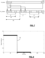
- the process commences at state 68 where initial configuration occurs. Controller proceeds to state 70. State 70 is a wait state for synchronizing the initial sampling in accordance with a pulse trigger edge. Upon detection of the pulse trigger edge, the process proceeds to state 72 in which sampling occurs at the sampling time t s (or sampling rate of 1110 Hz) and the samples are placed in a receive buffer R x . An example of receive buffer R x is shown in FIG. 7 . As seen in FIG.
- the samples stored in receive buffer R x are redistributed into bins of a reconstruction buffer R con , also shown in FIG. 7 . Values from each position in receive buffer R x are redistributed into the appropriate N bins of reconstruction buffer R con .
- the bins of the respective receive buffer R x and reconstruction buffer R con are of different widths.
- the bins of the reconstruction buffer R con and receive buffer R x are different sizes.
- the time based bins are constructed in terms of an index bin representation. Based on the pulse rate and the number of N samples acquired, a bin in reconstruction buffer R con may already contain a data value.
- reconstruction buffer R con of FIG. 7 facilitates recognizing a correspondence between different portions of reconstruction buffer R con and the waveform 60. More particularly, the bins of reconstruction buffer R con denoted by y r correspond to the rising portion of waveform 60 being reconstructed and are processed to yield the rise time ⁇ t r of waveform 60. Similarly, the bins of reconstruction buffer R con denoted by y f correspond to the falling portion of the waveform 60 being reconstructed and are processed to yield the fall time ⁇ t f of waveform 60.
- the bins of reconstruction buffer R con denoted by ⁇ correspond to the steady state or ON portion of waveform 60 following the rise of waveform 60, and ⁇ t s corresponds to the time for waveform 60 to settle to the steady state or ON portion.
- the samples K 1 ..., K M indicate the minimum number of bins to be filled in order to start the reconstruction process.
- ⁇ can be reported and processing can proceed.
- state 82 when bins y r and y f are full, information regarding the respective rising and falling edges and the respective rise and fall times can be reported including, for example, respective derivatives of the rise and fall times, ⁇ y r / ⁇ t r and ⁇ y f / ⁇ t f .
- the reported information can be information useful for further controlling RF power system 10, statistical information for operators, or other various uses.
- the reported information may be scalar values or data sequences, depending upon the particular implementation.
- FIG. 9 depicts an expanded block diagram 90 of power control module 40.
- power control module 40 includes a pulse control module or circuit 92, a ratio control module or circuit 94, and an edge control module or circuit 96.
- Pulse control module 92 communicates with ratio control module 94 via a communication 98.
- Pulse control module 92 communicates with edge control module 96 via a communication 100.
- Ratio control module 94 receives the respective voltage or current values pertaining to a desired output ratio, ⁇ m and ⁇ n , as inputs, described above with respect to equations (4) and (5).
- Pulse control module 92 communicates with power amplifier 20 and match controller 50 of matching network 14 via communication link 102.
- Each of communication links 98, 100, 102 may be implemented as a digital or analog communication link and in various embodiments may be implemented generally in a bus structure. Further, in various embodiments, pulse control module 92, ratio control module 94, and edge control module 96 may communicate directly with match controller 50, such as over communication link 23, using independent communication links or a bus structure.
- ratio control module 94 Upon receiving the ⁇ m and ⁇ n inputs, ratio control module 94 generates commands communicated to matching network 14 and match controller 50.
- Edge control module 96 receives the respective derivatives of the rise and fall times, ⁇ y r / ⁇ t r and ⁇ y f / ⁇ t f , and generates an edge control signal providing commands to allow for edge control or the RF pulse. In various embodiments, edge control module 96 utilizes the derivatives of the rise and fall times to generate commands to adjust the position of one of first tune element 56 and second tune element 58. In various embodiments, edge control module 96 varies the position of a selected tune element 56 in order to determine the rate of the rise and fall times.
- edge control module 96 generates commands used by match controller 50 to control the position of a tune capacitor, such as may be implemented by second tune element 58.
- edge control module 96 utilizes the respective derivatives of the rise and fall times, ⁇ y r / ⁇ t r and ⁇ y f / ⁇ t f input thereto and generates commands to vary the increase or decrease (or ramping) of RF signal 18 output by power amplifier 20 during transitions.
- Edge control module 96 generates commands to pulse control module 92, and pulse control module 92 generates commands directing power amplifier 20 to effect the appropriate increase or decrease (or ramping) of the pulse output by power amplifier 20.
- edge control module 96 generates commands to vary one or both of the rising or falling edges of a pulse signal and the increase or decreasing (ramping) transition of the RF signal 18.
- FIG. 10 depicts a generalized representation of a multi-level pulse waveform
- FIG. 11 depicts a receive buffer and a reconstruction buffer.
- the quantities shown in each of FIGS. 10 and 11 are used to indicate the relationship between the pulse waveform and portions of the reconstruction buffer.
- First falling (transition) portion 112 descends from first level 110 to a second level 114.
- Second level 114 corresponds to a settled or a steady state portion of multi-level pulse waveform 106.
- Multi-level pulse waveform 106 also includes a second falling (transition) portion 116. While multi-level pulse waveform 106 of FIG. 10 is shown as a two-level waveform, it should be recognized that multi-level pulse waveform 106 may be implemented having two or more levels, some of which may be zero or nonzero. In various embodiments, multi-level pulse waveform 106 may have multiple rising (transition) portions in addition to first rising (transition) portion 108.
- FIG. 11 indicates two data sequences, ⁇ a and ⁇ b , having respective values K 1 ..., K M and F 1 ..., F M .
- Data sequences ⁇ a and ⁇ b as compared to the single data sequence ⁇ of FIG. 7 enable the reconstruction of, for example, respective first level 110 and second level 114.
- data sequences ⁇ a and ⁇ b in the reconstruction buffer of FIG. 11 correspond to portions of respective first level 110 and second level 114.
- the data sequences of values K 1 ..., K M and F 1 ..., F M enable the determination of respective first portion 110 and second portion 114.
- data sequences ⁇ a and ⁇ b represent a selected section of respective first level 110 and second level 114.
- respective first level 110 and second level 114 can be determined by sampling a selected section of each level.
- data sequence y ra corresponds to a selected section of first rising (transition) portion 108.
- the change in time ⁇ t ra indicates the time duration of y ra
- ⁇ y ra indicates the change in amplitude of the of first rising portion 108.
- data sequence y fa corresponds to a selected section of first falling (transition) portion 112.
- the change in time ⁇ t fa indicates the time duration of y fa
- ⁇ y fa indicates the change in amplitude of the of first falling portion 112.
- Data sequence y fb corresponds to a selected section of first falling (transition) portion 114.
- the change in time ⁇ t fb indicates the time duration of y th
- ⁇ y fb indicates the change in amplitude of the of first falling portion 114.
- each settled or steady-state section of a pulse can have an associated rise and fall for which similar quantities can be determined.
- reconstruction of each rising and falling section can be accomplished by sampling a subset or selected section of the respective rising and falling (transition) portions of multi-level multi-level pulse waveform 106.
- edge control module 96 With reference to FIG. 9 , operation of edge control module 96 can be further described. As described above, edge control module generates commands to pulse control module 92, and pulse control module 92 generates commands directing power amplifier 20 to effect the appropriate increase or decrease (or ramping) of the pulse output by power amplifier 20.
- FIG. 10 with reference to portions 108, 112, and 114 of multi-level pulse waveform 106, provides a visual representation of controlling the increase or decrease (or ramping) of the pulse output by power amplifier 20. Rising portion 108 and falling portion 112 and 114 are depicted using a stair-stepped transition, where the amplitude or level) and duration of each increment or step can be varied by pulse edge controller to vary the ramping of each transition portion of multi-level pulse waveform 106. Controlling the stair-stepped transitions provides improved control of the pulse output by power amplifier 20. It should be recognized that the amplitude or level and duration of each increment or step of portions 108, 112, and 114 of multi-level can be independently determined.
- Spatial and functional relationships between elements are described using various terms, including “connected,” “engaged,” “coupled,” “adjacent,” “next to,” “on top of,” “above,” “below,” and “disposed.” Unless explicitly described as being “direct,” when a relationship between first and second elements is described in the above disclosure, that relationship can be a direct relationship where no other intervening elements are present between the first and second elements, but can also be an indirect relationship where one or more intervening elements are present (either spatially or functionally) between the first and second elements.
- the phrase at least one of A, B, and C should be construed to mean a logical (A OR B OR C), using a non-exclusive logical OR, and should not be construed to mean "at least one of A, at least one of B, and at least one of C.”
- the term 'module' or the term 'controller' may be replaced with the term 'circuit.
- the term 'module' may refer to, be part of, or include: an Application Specific Integrated Circuit (ASIC); a digital, analog, or mixed analog/digital discrete circuit; a digital, analog, or mixed analog/digital integrated circuit; a combinational logic circuit; a field programmable gate array (FPGA); a processor circuit (shared, dedicated, or group) that executes code; a memory circuit (shared, dedicated, or group) that stores code executed by the processor circuit; other suitable hardware components that provide the described functionality; or a combination of some or all of the above, such as in a system-on-chip.
- ASIC Application Specific Integrated Circuit
- FPGA field programmable gate array
- the module may include one or more interface circuits.
- the interface circuits may include wired or wireless interfaces that are connected to a local area network (LAN), the Internet, a wide area network (WAN), or combinations thereof.
- LAN local area network
- WAN wide area network
- the functionality of any given module of the present disclosure may be distributed among multiple modules that are connected via interface circuits. For example, multiple modules may allow load balancing.
- a server (also known as remote, or cloud) module may accomplish some functionality on behalf of a client module.
- code may include software, firmware, and/or microcode, and may refer to programs, routines, functions, classes, data structures, and/or objects.
- shared processor circuit encompasses a single processor circuit that executes some or all code from multiple modules.
- group processor circuit encompasses a processor circuit that, in combination with additional processor circuits, executes some or all code from one or more modules. References to multiple processor circuits encompass multiple processor circuits on discrete dies, multiple processor circuits on a single die, multiple cores of a single processor circuit, multiple threads of a single processor circuit, or a combination of the above.
- shared memory circuit encompasses a single memory circuit that stores some or all code from multiple modules.
- group memory circuit encompasses a memory circuit that, in combination with additional memories, stores some or all code from one or more modules.
- the term memory circuit is a subset of the term computer-readable medium.
- the term computer-readable medium does not encompass transitory electrical or electromagnetic signals propagating through a medium (such as on a carrier wave); the term computer-readable medium may therefore be considered tangible and non-transitory.
- Non-limiting examples of a non-transitory, tangible computer-readable medium are nonvolatile memory circuits (such as a flash memory circuit, an erasable programmable read-only memory circuit, or a mask read-only memory circuit), volatile memory circuits (such as a static random access memory circuit or a dynamic random access memory circuit), magnetic storage media (such as an analog or digital magnetic tape or a hard disk drive), and optical storage media (such as a CD, a DVD, or a Blu-ray Disc).
- nonvolatile memory circuits such as a flash memory circuit, an erasable programmable read-only memory circuit, or a mask read-only memory circuit
- volatile memory circuits such as a static random access memory circuit or a dynamic random access memory circuit
- magnetic storage media such as an analog or digital magnetic tape or a hard disk drive
- optical storage media such as a CD, a DVD, or a Blu-ray Disc
- the apparatuses and methods described in this application may be partially or fully implemented by a special purpose computer created by configuring a general purpose computer to execute one or more particular functions embodied in computer programs.
- the functional blocks and flowchart elements described above serve as software specifications, which can be translated into the computer programs by the routine work of a skilled technician or programmer.
- the computer programs include processor-executable instructions that are stored on at least one non-transitory, tangible computer-readable medium.
- the computer programs may also include or rely on stored data.
- the computer programs may encompass a basic input/output system (BIOS) that interacts with hardware of the special purpose computer, device drivers that interact with particular devices of the special purpose computer, one or more operating systems, user applications, background services, background applications, etc.
- BIOS basic input/output system
- the computer programs may include: (i) descriptive text to be parsed, such as HTML (hypertext markup language) or XML (extensible markup language), (ii) assembly code, (iii) object code generated from source code by a compiler, (iv) source code for execution by an interpreter, (v) source code for compilation and execution by a just-in-time compiler, etc.
- source code may be written using syntax from languages including C, C++, C#, Objective C, Haskell, Go, SQL, R, Lisp, Java ® , Fortran, Perl, Pascal, Curl, OCaml, Javascript ® , HTML5, Ada, ASP (active server pages), PHP, Scala, Eiffel, Smalltalk, Erlang, Ruby, Flash ® , Visual Basic ® , Lua, and Python ® .
Landscapes
- Physics & Mathematics (AREA)
- Engineering & Computer Science (AREA)
- Plasma & Fusion (AREA)
- Chemical & Material Sciences (AREA)
- Analytical Chemistry (AREA)
- Electromagnetism (AREA)
- Spectroscopy & Molecular Physics (AREA)
- Plasma Technology (AREA)
- Amplifiers (AREA)
- Control Of Amplification And Gain Control (AREA)
- Power Engineering (AREA)
Description
- The present disclosure relates to radio frequency (RF) power delivery systems and to centralized control of RF impedance matching networks.
- The background description provided here is for the purpose of generally presenting the context of the disclosure.
- Plasma etching is frequently used in semiconductor fabrication. In plasma etching, ions are accelerated by an electric field to etch exposed surfaces on a substrate. The electric field is generated based on RF power signals generated by a radio frequency (RF) generator of a RF power system. The RF power signals generated by the RF generator must be precisely controlled to effectively execute plasma etching.
- A RF power system may include a RF generator, a matching network and a load (e.g., a plasma chamber). The RF generator generates RF power signals, which are received at the matching network. The matching network matches an input impedance of the matching network to a characteristic impedance of a transmission line between the RF generator and the matching network. This impedance matching aids in maximizing an amount of power forwarded to the matching network ("forward power") and minimizing an amount of power reflected back from the matching network to the RF generator ("reverse power"). Forward power may be maximized and reverse power may be minimized when the input impedance of the matching network matches the characteristic impedance of the transmission line.
- In the RF power supply field, there are typically two approaches to applying the RF signal to the load. A first, more traditional approach is to apply a continuous wave signal to the load. In a continuous wave mode, the continuous wave signal is typically a sinusoidal wave that is output continuously by the power supply to the load. In the continuous wave approach, the RF signal assumes a sinusoidal output, and the amplitude and/or frequency of the sinusoidal wave can be varied in order to vary the output power applied to the load.
- A second approach to applying the RF signal to the load involves pulsing the RF signal, rather than applying a continuous wave signal to the load. In a pulse mode of operation, a RF sinusoidal signal is modulated by a modulation signal in order to define an envelope for the modulated sinusoidal signal. In a conventional pulse modulation scheme, the RF sinusoidal signal typically is output at a constant frequency and amplitude. Power delivered to the load is varied by varying the modulation signal, rather than varying the sinusoidal, RF signal.
- In the typical RF power supply configuration, output power applied to the load is determined by using sensors that measure the forward and reflected power or the voltage and current of the RF signal applied to the load. Either set of these signals is analyzed in a typical feedback loop. The analysis typically determines a power value which is used to adjust the output of the RF power supply in order to vary the power applied to the load. In a RF power delivery system, where the load is a plasma chamber, the varying impedance of the load causes a corresponding varying power applied to the load, as applied power is in part a function of the impedance of the load.
- As plasma systems have evolved, many new challenges exist to meet the specifications required to meet critical manufacturing specifications for both continuous wave and pulsed RF control. One advance includes applying a single output from the RF generator to a matching network and providing multiple RF feeds to plasma chambers to allow for increased control of various plasma parameters. In an exemplary configuration, a RF generator provides a single input to the matching network, and the matching network provides multiple RF feeds to corresponding multiple electrodes of one or multiple plasma chambers.
- Further, the transition from continuous wave RF power delivery systems to pulse RF power delivery systems presents additional challenges. In a typical plasma system, the power dissipated in the plasma depends upon the impedance of the plasma. If the impedance varies in relation to the timescale of the RF pulse (typically in the range of 1 kHz-10 kHz), so as to not extinguish the plasma between pulse events, the sensors and actuators in the matching network and generator must respond on a similar timescale to provide optimal power coupling to the plasma load. Further, the time response of the impedance is plasma dependent and varies in accordance with factors such as chemistry, pressure, and power coupling. Further yet, the various parasitic elements outside of the plasma, such as resistive loss in the RF coupling antenna or the match system, present a time varying power coupling efficiency during the pulse cycle because they are a constant dissipated impedance in series with a time varying impedance load. Further yet, because the transmitted and reflected power sensors and RF generators are typically calibrated for a matched termination, power compensation due to impedance mismatch can contribute to increased variability in power delivery.
- In the present, conventional control approach, the RF power supply and the matching network function independently. The RF power supply controls the RF output to the matching network, and the matching network independently controls tuning of the match elements to provide an impedance match. The matching network also controls the relative output between the multiple outputs from the matching network applied to the respective multiple electrodes of the one or multiple plasma chambers.
- The conventional approach has various cost and complexity limitations in connection with both continuous wave and pulse mode operation. For example, the RF metrology requirements for the input and output of the impedance matching device are increased. Further, for frequency tuning systems, the RF metrology of the impedance matching network requires frequency tracking to scale the sampled RF to the operating frequency and synchronization with the RF generator to alleviate aliasing and control latency issues. The conventional approach also requires that the matching network includes computing resources to perform the ratio control functionality, also adding cost and complexity. Further yet, and further adding cost and complexity, in order to minimize undesirable RF transients, the RF generator and matching network must be coordinated for proper RF power regulation. Present, conventional systems also require synchronization of the RF output measurements, which typically occurs at the matching network. The above challenges are further increased in connection with pulse mode operation.
-
US 8282983 B1 describes apparatus and methods to minimize wafer-to-wafer process variation in RF-based semiconductor processing reactors with shared RF source for multiple processing areas. RF sensors associated with each processing area sends signal to the RF balance controller. The controller modifies station impedance using power adjustment mechanisms. As a result, station to station distribution of a selected RF parameter (e.g., load power) may match the station set points. Closed loop control maintains balance despite changing conditions. -
WO 2009/099486 A1 describes a system and method for delivering power to a dynamic load. The system includes a power supply providing DC power having a substantially constant power open loop response, a power amplifier for converting the DC power to RF power, a sensor for measuring voltage, current and phase angle between voltage and current vectors associated with the RF power, an electrically controllable impedance matching system to modify the impedance of the power amplifier to at least a substantially matched impedance of a dynamic load, and a controller for controlling the electrically controllable impedance matching system. The system further includes a sensor calibration measuring module for determining power delivered by the power amplifier, an electronic matching system calibration module for determining power delivered to a dynamic load, and a power dissipation module for calculating power dissipated in the electrically controllable impedance matching system. -
US 2010/0194195 A1 describes a radio frequency (RF) system which includes a control module that allocates M predetermined frequency intervals. The system also includes N RF sources that each applies first RF power to electrodes within a plasma chamber at frequencies within an assigned respective one of the M predetermined frequency intervals. The N RF sources also each respond to second RF power including feedback from the plasma chamber. The N RF sources each include a processing module that adjusts the first RF power based on the second RF power and the respective one of the M predetermined frequency intervals. M and N are integers greater than 1.US 2013/0105086 A1 discloses a plasma processing apparatus including a process chamber having an interior processing volume, and first, second and third RF coils disposed proximate the process chamber to couple RF energy into the processing volume. The RF power source is a single RF power source and provides RF power to each of the first, second, and third RF coils. A power divider is provided to adjust the RF power respectively delivered to two or more of the first, second, and third RF coils. - Also relevant to the technological background is DAVID J. COUMOU: "Feedforward power distortion correction in RF power delivery systems for plasma processing systems" 2012 18th IEEE-NPSS Real Time Conference (RT 2012) : Berkeley, California, USA, 9 - 15 June 2012, 20120601; 1077952576 - 1077952576 IEEE, Piscataway, NJ
- This section provides a general summary of the disclosure, and is not a comprehensive disclosure of its full scope or all of its features.
-
Claim 1 defines a radio frequency (RF) control system - Claim 11 defines a method for controlling a radio frequency (RF) control system.
- Further areas of applicability will become apparent from the description provided herein. The description and specific examples in this summary are intended for purposes of illustration only and are not intended to limit the scope of the present disclosure.
- The drawings described herein are for illustrative purposes only of selected embodiments and not all possible implementations, and are not intended to limit the scope of the present disclosure.
-
FIG. 1 depicts a functional block diagram of the RF power delivery control system incorporating the unified RF power delivery single input, multiple output control in accordance with the present disclosure; -
FIG. 2 depicts a waveform of an exemplary output pulse to be reconstructed in accordance with the present disclosure; -
FIG. 3 depicts a pulse and exemplary waveforms bounded by the pulse in accordance with operation of a RF generator in a pulse mode of operation; -
FIG. 4 depicts an exemplary, aliased waveform of the output pulse ofFIG. 2 ; -
FIG. 5 depicts the waveform ofFIG. 4 having an expanded time scale; -
FIG. 6 depicts a state diagram of a portion of the RF power delivery control system incorporating the unified RF power delivery single input, multiple output control for reconstructing an output pulse and a pulse mode RF power delivery system; -
FIG. 7 depicts a receive buffer and a reconstruction buffer for reconstructing the RF output pulse signal; -
FIG. 8 depicts a single cycle of a waveform reconstructing from the waveform ofFIG. 3 using the method depicted in the state diagram ofFIG. 6 ; -
FIG. 9 depicts an expanded block diagram of control portion of the RF controller ofFIG. 1 ; -
FIG. 10 is a more generalized representation of the reconstruction buffer ofFIG. 7 for use in connection with a more generalized configuration of a pulse waveform; and -
FIG. 11 depicts a multi-level pulse waveform quantities used to describe the reconstruction buffer in order to demonstrate the relationship between the sample pulse waveform and the reconstruction buffer. - Corresponding reference numerals indicate corresponding parts throughout the several views of the drawings, and reference numbers may be reused to identify similar and/or identical elements.
- Example embodiments will now be described more fully with reference to the accompanying drawings.
- Example embodiments are provided so that this disclosure will be thorough, and will fully convey the scope to those who are skilled in the art. Numerous specific details are set forth such as examples of specific components, devices, and methods, to provide a thorough understanding of embodiments of the present disclosure. It will be apparent to those skilled in the art that specific details need not be employed, that example embodiments may be embodied in many different forms and that neither should be construed to limit the scope of the disclosure. In some example embodiments, well-known processes, well-known device structures, and well-known technologies are not described in detail.
- The terminology used herein is for the purpose of describing particular example embodiments only and is not intended to be limiting. As used herein, the singular forms "a," "an," and "the" may be intended to include the plural forms as well, unless the context clearly indicates otherwise. The terms "comprises," "comprising," "including," and "having," are inclusive and therefore specify the presence of stated features, integers, steps, operations, elements, and/or components, but do not preclude the presence or addition of one or more other features, integers, steps, operations, elements, components, and/or groups thereof. The method steps, processes, and operations described herein are not to be construed as necessarily requiring their performance in the particular order discussed or illustrated, unless specifically identified as an order of performance. It is also to be understood that additional or alternative steps may be employed.
- When an element or layer is referred to as being "on," "engaged to," "connected to," or "coupled to" another element or layer, it may be directly on, engaged, connected or coupled to the other element or layer, or intervening elements or layers may be present. In contrast, when an element is referred to as being "directly on," "directly engaged to," "directly connected to," or "directly coupled to" another element or layer, there may be no intervening elements or layers present. Other words used to describe the relationship between elements should be interpreted in a like fashion (e.g., "between" versus "directly between," "adjacent" versus "directly adjacent," etc.). As used herein, the term "and/or" includes any and all combinations of one or more of the associated listed items.
- Although the terms first, second, third, etc. may be used herein to describe various elements, components, regions, layers and/or sections, these elements, components, regions, layers and/or sections should not be limited by these terms. These terms may be only used to distinguish one element, component, region, layer or section from another region, layer or section. Terms such as "first," "second," and other numerical terms when used herein do not imply a sequence or order unless clearly indicated by the context. Thus, a first element, component, region, layer or section discussed below could be termed a second element, component, region, layer or section without departing from the teachings of the example embodiments.
- Spatially relative terms, such as "inner," "outer," "beneath," "below," "lower," "above," "upper," and the like, may be used herein for ease of description to describe one element or feature's relationship to another element(s) or feature(s) as illustrated in the figures. Spatially relative terms may be intended to encompass different orientations of the device in use or operation in addition to the orientation depicted in the figures. For example, if the device in the figures is turned over, elements described as "below" or "beneath" other elements or features would then be oriented "above" the other elements or features. Thus, the example term "below" can encompass both an orientation of above and below. The device may be otherwise oriented (rotated 90 degrees or at other orientations) and the spatially relative descriptors used herein interpreted accordingly.
- In
FIG. 1 , a RF power system including a RF control orpower system 10 is shown.RF power system 10 includes aRF generator 12, amatching network 14, and a plurality ofloads matching network 14.RF generator 12 generates aRF power signal 18, which is provided to matchingnetwork 14.Matching network 14 matches an input impedance of matchingnetwork 14 to a characteristic impedance of a transmission line between theRF generator 12 andmatching network 14. Put another way, matchingnetwork 14 matches an impedance ofload 16 to an impedance as seen by the output ofRF generator 12.Matching network 14 andload 16 may be considered as the load on theRF generator 12.Loads load 16 may be static (i.e. unchanging over time) or dynamic (i.e. changing over time). -
RF generator 12 includes a RF power source orpower amplifier 20 and a first orinternal feedback loop 22a and a second or external feedback loop22b. Power amplifier 20 generatesRF power signal 18, which is output to matchingnetwork 14.Power amplifier 20 may generate theRF power signal 18 based on a power signal received from a power source (not shown) external topower amplifier 20. The power source may be external to theRF generator 12. The power source may be, for example, a direct current (DC) power source. - First or
internal feedback loop 22a includes one or more sensors (first sensors) 26 that generate signals X and Y (also 30) input tocontroller 28 ofpower amplifier 20.Internal feedback loop 22a also includes ascaling module 32, asummer 36, and apower control module 40.Sensors 26 may include voltage, current, and/or directional coupler sensors.Sensors 26 may detect (i) voltage V and current I output ofpower amplifier 20, and/or (ii) forward (or source) power PFWD out ofpower amplifier 20 and/orRF generator 12 and reverse (or reflected) power PREV received from matchingnetwork 14. The voltage V, current I, forward power PFWD, and reverse power PREV may be scaled and/or filtered versions of the actual voltage, current, forward power and reverse power of the output of thepower amplifier 20. Thesensors 26 may be analog and/or digital sensors. In a digital implementation, thesensors 26 may include analog-to-digital (A/D) converters and signal sampling components with corresponding sampling rates. Signals X and Y can represent any of the voltage V and current I or forward (or source) power PFWD and reverse (or reflected) power PREV. -
Sensors 26 generate sensor signals X, Y, which are received by scalingmodule 32.Scaling module 32 scales sensor signals 30 and generates apower feedback signal 34.Power feedback signal 34 is generated based on the sensor signals 30 and a scaling matrix. Thepower feedback signal 34 may, for example, represent the forward power for forward power leveling power delivery.Power feedback signal 34 may represent the RF power transferred to thematching network 14 or load power Pd and can be represented by equation (1), where V is voltage output of thepower amplifier 20 and/orRF generator 12, I is current out of thepower amplifier 20 and/orRF generator 12, and Θ is a phase difference between the voltage and the current outputs V, I of thepower amplifier 20.
-
Summer 36 sums thepower feedback signal 34 with a predeterminedpower setpoint signal 38, which may be generated by a power setpoint module (not shown).Power feedback signal 34 may be subtracted from the predeterminedpower setpoint signal 38 to generate an error signal efb . -
Power control module 40 receives the error signal efb and generates a power control signal
power amplifier 20. Power control signal
power amplifier 20.Power amplifier 20 adjustsRF power signal 18 based on power control signal
RF power signal 18 may be a continuous waveform or a pulse waveform.Power control module 40 may include a proportional integral derivative (PID) controller or subset thereof and/or a direct digital synthesis (DDS) component(s). In various implementations,power control module 40 is a first PID controller or subset thereof with a function identified as

-
Matching network 14 includes a tuning andratio actuator 48 and amatch controller 50. Tuning network andratio actuator 48 includes tuning elements for varying the impedance at the output ofRF generator 12 in order to respond to variations inload 16 and maintain a stable impedance at the output ofRF generator 12. Tuning network andratio actuator 48, for example, includes one or both of a firstmatch tuning element 56 and a secondmatch tuning element 58, each of which are adjustable in order to vary the impedance at matchingnetwork 14 to maintain a match condition. In various embodiments, tuning network andratio actuator 48 includes one or both of a load capacitance that corresponds tofirst tune element 56 and a tune capacitance that corresponds tosecond tune element 58. Each of the tune capacitance and the load capacitance are adjustable in order to vary the impedance at matchingnetwork 14 to tune to and maintain a match condition. Tuning network andratio actuator 48 also includes one or moreratio tuning element 59.Ratio element 59 enables tuning network andratio actuator 48 to vary the output of RF power output to selectedtransmission lines respective loads -
Matching network 14 also includes a plurality ofRF sensors transmission lines ratio actuator 48. RF sensors 54 operate similarly as described with respect toRF sensor 26 ofRF generator 12.RF sensors respective transmission lines controller 50.Match controller 50 communicates a characteristic signal that varies in accordance with the information sensed by respective RF sensors 54 tocontroller 28 ofRF generator 12 overcommunication link 23. - Various techniques are disclosed herein that include maximizing optimal power transfer in a RF power system with a dynamic load (i.e. a load having varying impedance(s)). A first technique includes
RF power amplifier 20 connected to matchingnetwork 14.Matching network 14 may include an impedance matching network andratio actuator 48 to effect one or both ratio control between any two selectedloads RF generator 12match network 14. - For example, tuning network and
ratio actuator 48 includes two or morevariable tuning elements Variable tuning elements RF generator 12 and one tune capacitance in series with load 16).Variable tuning elements matching network 14, and may have respectively an associated tune input and load input. The tune and load parameters refer to impedance adjustments performed in matchingnetwork 14 via the variable tuning elements. As an example, the tune parameter and the load parameter may be associated with respective capacitances of capacitors in matchingnetwork 14. In various embodiments, a second technique introduces a variable frequency adjustment to thepower amplifier 20 and may be used alternatively or in combination with the first technique. The tune and load parameters may each be fixed, discretely selectable, and/or adjustable when using the second technique. - In both the first and second techniques, the RF power transferred Pd from the
power amplifier 20 to thematching network 14 is maximized. This may occur when the forward power PFWD to thematching network 14 is maximized and/or the reverse power PREV from the matching network is minimized. The RF power transferred Pd may be represented by equation (2). A maximum RF power transferred PMAX may be represented by equation (3).

- The RF power transferred Pd is maximized when the phase Θ is as close to zero as systematically achievable for a
RF power system 10 providing power to a reactive load or reactive impedance (e.g. load 16). A reactive impedance refers to a load with changing impedance. The first and second techniques minimize the phase Θ by adjusting the tune and load parameters of thematching network 14. Since the phase Θ is dependent on the reactive impedance, reduction in the phase Θ is a function of frequency f of thepower amplifier 20. As a result, phase reduction can be performed as a function of the frequency f or in other words, the phase Θ can be reduced to or nearly 0 by adjusting the frequency f of thepower amplifier 20 and thus the output frequency f of thepower amplifier 20. - As mentioned above,
RF generator 12 also includes a second orexternal feedback loop 22b.Second feedback loop 22b includes sensor 54,match controller 50, andpower control module 40 ofcontroller 28. As described above, sensor 54 generates signals similar to X and Y output byRF sensor 26. The signals output by sensor 54 are input to matchcontroller 50.Match controller 50 processes the received signals and outputs information characteristic of the signals tocontroller 28 ofRF generator 12. The information output bymatch controller 50 is output in a digital format tocontroller 28. - In a conventional configuration, a matching network operating independently of the RF generator includes circuitry to adjust the respective tuning element or elements in accordance with the determined match condition. Likewise, in a conventional configuration, the matching network will receive commands from an external source about the desired, predetermined ratio of the output applied to
respective loads respective loads - In the various embodiments described in the present disclosure, however,
RF generator 12 controls both thetuning elements output ratio element 59 in a unified manner bycontroller 28 ofRF generator 12. Control of thefirst tuning element 56 andsecond tuning element 58 is described inUS 8576013 B2 entitled Power Distortion-Based Servo Control Systems for Frequency Tuning RF Power Sources, granted November 5, 2013, and assigned to the assignee of the present application. Control of thefirst tuning element 56 andsecond tuning element 58 can occur whencontroller 28 outputs and communicates a tune control signal to matchcontroller 50 to effect tuning of the respectivefirst tuning element 56 andsecond tuning element 58. In various embodiments,power control module 40 ofcontroller 28 controls the power ratio of the RF outputs from matchingnetwork 14 applied torespective loads -
Power control module 40 ofcontroller 28 utilizes the information received frommatch controller 50, insecond feedback loop 22b, received from RF sensor 54.Match controller 50 communicates withcontroller 28 in various embodiments at fixed data rates and link latency to provide information characterizing the outputs to load 16. From these values,RF generator 12 computes a ratio for a particular output σr(i) (such as to one ormore loads 
- m is a first output from matching
network 14, - n is an nth output from matching
network 14, - £ is the ith voltage or current value pertaining to a desired output ratio, xr , for the corresponding matching network m of n outputs.
-
Power control module 40 utilizes a digital controller

power control module 40 implements a proportional control approach to determine actuator position λ. Proportional control for the computation of the actuator position λ, can be described as shown in equation (7)
- λ(i + 1) is the new calculated value of λ,
- λ(i) is a the prior calculated value of λ, and
- G is a variable or constant parameter for the proportional or gain control equation.
- λ(i + 1), λ(i), and G are as described above,
- e(i - 1) and e(i - 2) are the first and second respective prior error terms,
- α, β, and γ are variable or constant terms for the control equation.
- The unified ratio control approach described above may be generalized to both the continuous wave and a pulse mode operation of
RF generator 12. However, pulse mode operation introduces other considerations that must be addressed in order to effectively implement unified ratio control. Sampling of the waveform of the RF output applied toloads 16 and information to be communicated frommatch controller 50 tocontroller 28 are considered in connection withFIGS. 2-9 . When the output fromRF generator 12 is pulsed, sampled signals from sensor 54 are asynchronous to the RF output frompower amplifier 20. A signal reconstructed from the pulse signals at the outputs of matchingnetwork 14 to transmission line 52 will be phase shifted with respect to the pulse output fromRF generator 12. Accordingly,FIGS. 2-9 described an approach in whichcontroller 28 reconstructs a pulse mode signal output from matchingnetwork 14 while accounting for the asynchronous nature of the reconstruction. -
FIG. 2 depicts apulse waveform 60, such as may be output on transmission line 52.FIG 3 . depicts a general representation of apulse waveform 60. As can be seen inFIG. 3 ,pulse waveform 60 provides an envelope for a sinusoidal voltage signal V(t) and sinusoidal current signal I(t), so that whenwaveform 60 is on, the sinusoidal signals V(t) and I(t) are bounded bywaveform 60 and may be output. Whenwaveform 60 is off (having an amplitude of zero), no output occurs and sinusoidal signals V(t) and I(t) are both zero. In one non-limiting example, as shown inFIG. 2 ,pulse waveform 60 has a frequency or pulse repetition frequency (PRF) of 500 kHz, or a pulse rate time (tp ) of 200 µs. That is tp = PRF-1. Ifpulse waveform 60 is sampled at a sampling rate of 1110 Hz, i.e., the sampling time ts = 1/1110 s, analiased representation 62 ofpulse waveform 60 results, as shown in the waveforms ofFIGS. 4 and 5 , withFIG. 5 showing an expanded timescale ofFIG. 4 . Althoughpulse waveform 60 shown inFIG. 2 , is represented as a square wave,pulse waveform 60 may be a square, sawtooth, triangular, bi-level or multi-level, and other wave shapes.Pulse waveform 60 is periodic in various embodiments. - The state diagram 66 of
FIG. 6 depicts various embodiments for reconstructingpulse waveform 60. This reconstruction accounts for latency in the sample waveform and for the nature of the aliasedrepresentation 62 ofwaveform 60, as shown inFIGS. 4 and 5 . The process commences atstate 68 where initial configuration occurs. Controller proceeds tostate 70.State 70 is a wait state for synchronizing the initial sampling in accordance with a pulse trigger edge. Upon detection of the pulse trigger edge, the process proceeds tostate 72 in which sampling occurs at the sampling time ts (or sampling rate of 1110 Hz) and the samples are placed in a receive buffer Rx. An example of receive buffer Rx is shown inFIG. 7 . As seen inFIG. 7 , receive buffer Rx comprises N samples occurring every ts seconds and has total length of Ts = Nts seconds. Each sample is placed in the appropriate position in receive buffer Rx in accordance with particular time of the sampling relative to ts = 0. The samples stored in receive buffer Rx are redistributed into bins of a reconstruction buffer Rcon, also shown inFIG. 7 . Values from each position in receive buffer Rx are redistributed into the appropriate N bins of reconstruction buffer Rcon. The bins of the respective receive buffer Rx and reconstruction buffer Rcon are of different widths. Reconstruction buffer Rcon comprises N bins, but has a width of TPRF = Ntp seconds. Recall that for the example described herein, receive buffer Rx has a length of Ts = Nts seconds and that tp= 200 µs, while ts = 901 µs. Thus the bins of the reconstruction buffer Rcon and receive buffer Rx are different sizes. - Filling reconstruction buffer Rcon, occurs at
state 74. A predefined transfer function, such as a modulus function provides a mapping from receive buffer Rx to reconstruction buffer Rcon in accordance with equation (9)

state 76 where the data in each bin of reconstruction buffer Rcon is normalized by the number of samples accumulated in each bin. Normalization may occur by computing an average for each bin. After the acquisition of the entire N samples is completed, control returns toreconstruction state 74 where waveform is reconstructed.FIG. 8 depicts awaveform 88 reconstructed in accordance with the state diagram ofFIG. 6 . Once reconstruction buffer Rcon is filled, control can proceed tostate 78 and results of the reconstruction process are reported. - Further review of reconstruction buffer Rcon of
FIG. 7 facilitates recognizing a correspondence between different portions of reconstruction buffer Rcon and thewaveform 60. More particularly, the bins of reconstruction buffer Rcon denoted by yr correspond to the rising portion ofwaveform 60 being reconstructed and are processed to yield the rise time Δtr ofwaveform 60. Similarly, the bins of reconstruction buffer Rcon denoted by yf correspond to the falling portion of thewaveform 60 being reconstructed and are processed to yield the fall time Δtf ofwaveform 60. The bins of reconstruction buffer Rcon denoted by ξ correspond to the steady state or ON portion ofwaveform 60 following the rise ofwaveform 60, and Δtscorresponds to the time forwaveform 60 to settle to the steady state or ON portion. The samples K1..., KM indicate the minimum number of bins to be filled in order to start the reconstruction process. Referring tostate 80 ofFIG. 6 , once the ξ bins are filled, ξ̂ can be reported and processing can proceed. Similarly, referring tostate 82, when bins yr and yf are full, information regarding the respective rising and falling edges and the respective rise and fall times can be reported including, for example, respective derivatives of the rise and fall times, Δyr/Δtr and Δyf/Δtf. The reported information can be information useful for further controllingRF power system 10, statistical information for operators, or other various uses. The reported information may be scalar values or data sequences, depending upon the particular implementation. -
FIG. 9 depicts an expanded block diagram 90 ofpower control module 40. In the expanded block diagram 90,power control module 40 includes a pulse control module orcircuit 92, a ratio control module orcircuit 94, and an edge control module orcircuit 96.Pulse control module 92 communicates withratio control module 94 via acommunication 98.Pulse control module 92 communicates withedge control module 96 via acommunication 100.Ratio control module 94 receives the respective voltage or current values pertaining to a desired output ratio, ξm and ξn, as inputs, described above with respect to equations (4) and (5).Pulse control module 92 communicates withpower amplifier 20 andmatch controller 50 of matchingnetwork 14 viacommunication link 102. Each ofcommunication links pulse control module 92,ratio control module 94, andedge control module 96 may communicate directly withmatch controller 50, such as overcommunication link 23, using independent communication links or a bus structure. - Upon receiving the ξm and ξn inputs,
ratio control module 94 generates commands communicated to matchingnetwork 14 andmatch controller 50.Edge control module 96 receives the respective derivatives of the rise and fall times, Δyr/Δtr and Δyf/Δtf, and generates an edge control signal providing commands to allow for edge control or the RF pulse. In various embodiments,edge control module 96 utilizes the derivatives of the rise and fall times to generate commands to adjust the position of one offirst tune element 56 andsecond tune element 58. In various embodiments,edge control module 96 varies the position of a selectedtune element 56 in order to determine the rate of the rise and fall times. By varying the sharpness of the rising or falling edges, more accurate control of the process occurring inload 16 is achieved. Such control can be independent of or coincident with frequency tuning to arrive at an appropriate match condition. In various embodiments,edge control module 96 generates commands used bymatch controller 50 to control the position of a tune capacitor, such as may be implemented bysecond tune element 58. - In various embodiments,
edge control module 96 utilizes the respective derivatives of the rise and fall times, Δyr/Δtr and Δyf/Δtf input thereto and generates commands to vary the increase or decrease (or ramping) ofRF signal 18 output bypower amplifier 20 during transitions.Edge control module 96 generates commands topulse control module 92, andpulse control module 92 generates commands directingpower amplifier 20 to effect the appropriate increase or decrease (or ramping) of the pulse output bypower amplifier 20. In various embodiments,edge control module 96 generates commands to vary one or both of the rising or falling edges of a pulse signal and the increase or decreasing (ramping) transition of theRF signal 18. -
FIG. 10 depicts a generalized representation of a multi-level pulse waveform, andFIG. 11 depicts a receive buffer and a reconstruction buffer. The quantities shown in each ofFIGS. 10 and 11 are used to indicate the relationship between the pulse waveform and portions of the reconstruction buffer. Themulti-level pulse waveform 106 ofFIG. 11 includes a number of generally distinct portions. More particularly,multi-level pulse waveform 106 includes a first rising (transition)portion 108 starting at the time t = 0 and rising to afirst level 110.First level 110 corresponds to a settled or a steady state portion ofmulti-level pulse waveform 106.Multi-level pulse waveform 106 also includes a first falling (transition)portion 112. First falling (transition)portion 112 descends fromfirst level 110 to asecond level 114.Second level 114 corresponds to a settled or a steady state portion ofmulti-level pulse waveform 106.Multi-level pulse waveform 106 also includes a second falling (transition)portion 116. Whilemulti-level pulse waveform 106 ofFIG. 10 is shown as a two-level waveform, it should be recognized thatmulti-level pulse waveform 106 may be implemented having two or more levels, some of which may be zero or nonzero. In various embodiments,multi-level pulse waveform 106 may have multiple rising (transition) portions in addition to first rising (transition)portion 108. - In contrast to
FIG. 7 ,FIG. 11 indicates two data sequences, ξa and ξb , having respective values K1..., KM and F1..., FM. Data sequences ξa and ξb , as compared to the single data sequence ξ ofFIG. 7 enable the reconstruction of, for example, respectivefirst level 110 andsecond level 114. As can be seen inFIGS. 10 and 11 , data sequences ξa and ξb in the reconstruction buffer ofFIG. 11 correspond to portions of respectivefirst level 110 andsecond level 114. Thus, the data sequences of values K1..., KM and F1..., FM enable the determination of respectivefirst portion 110 andsecond portion 114. It should be noted that, as shown inFIG. 10 , data sequences ξa and ξb represent a selected section of respectivefirst level 110 andsecond level 114. Thus, respectivefirst level 110 andsecond level 114 can be determined by sampling a selected section of each level. - Also shown in
FIG 10 , data sequence yra corresponds to a selected section of first rising (transition)portion 108. The change in time Δtra indicates the time duration of yra, and Δyra indicates the change in amplitude of the of first risingportion 108. Similarly, data sequence yfa corresponds to a selected section of first falling (transition)portion 112. The change in time Δtfa indicates the time duration of yfa, and Δyfa indicates the change in amplitude of the of first fallingportion 112. Data sequence yfb corresponds to a selected section of first falling (transition)portion 114. The change in time Δtfb indicates the time duration of yth, and Δyfb indicates the change in amplitude of the of first fallingportion 114. While no second rise (transition) portion ofmulti-level pulse waveform 106 is shown inFIG. 10 , in various configurations of a multi-level pulse, each settled or steady-state section of a pulse can have an associated rise and fall for which similar quantities can be determined. As described above with respect to data sequences ξa and ξb , reconstruction of each rising and falling section can be accomplished by sampling a subset or selected section of the respective rising and falling (transition) portions of multi-levelmulti-level pulse waveform 106. - With reference to
FIG. 9 , operation ofedge control module 96 can be further described. As described above, edge control module generates commands topulse control module 92, andpulse control module 92 generates commands directingpower amplifier 20 to effect the appropriate increase or decrease (or ramping) of the pulse output bypower amplifier 20.FIG. 10 , with reference toportions multi-level pulse waveform 106, provides a visual representation of controlling the increase or decrease (or ramping) of the pulse output bypower amplifier 20. Risingportion 108 and fallingportion multi-level pulse waveform 106. Controlling the stair-stepped transitions provides improved control of the pulse output bypower amplifier 20. It should be recognized that the amplitude or level and duration of each increment or step ofportions - The foregoing description is merely illustrative in nature and is in no way intended to limit the disclosure, its application, or uses. The broad teachings of the disclosure can be implemented in a variety of forms. Therefore, while this disclosure includes particular examples, the scope of the disclosure should not be so limited since other modifications will become apparent upon a study of the drawings, the specification, and the following claims. It should be understood that one or more steps within a method may be executed in different order (or concurrently) without altering the principles of the present disclosure as long as within the extent of the present invention, which is determined by the claims. Further, although each of the embodiments is described above as having certain features, any one or more of those features described with respect to any embodiment of the disclosure can be implemented in and/or combined with features of any of the other embodiments, even if that combination is not explicitly described as long as within the extent of the present invention, which is determined by the claims. In other words, the described embodiments are not mutually exclusive, and permutations of one or more embodiments with one another remain within the scope of this disclosure as long as within the extent of the present invention, which is determined by the claims.
- Spatial and functional relationships between elements (for example, between modules, circuit elements, semiconductor layers, etc.) are described using various terms, including "connected," "engaged," "coupled," "adjacent," "next to," "on top of," "above," "below," and "disposed." Unless explicitly described as being "direct," when a relationship between first and second elements is described in the above disclosure, that relationship can be a direct relationship where no other intervening elements are present between the first and second elements, but can also be an indirect relationship where one or more intervening elements are present (either spatially or functionally) between the first and second elements. As used herein, the phrase at least one of A, B, and C should be construed to mean a logical (A OR B OR C), using a non-exclusive logical OR, and should not be construed to mean "at least one of A, at least one of B, and at least one of C."
- In this application, including the definitions below, the term 'module' or the term 'controller' may be replaced with the term 'circuit.' The term 'module' may refer to, be part of, or include: an Application Specific Integrated Circuit (ASIC); a digital, analog, or mixed analog/digital discrete circuit; a digital, analog, or mixed analog/digital integrated circuit; a combinational logic circuit; a field programmable gate array (FPGA); a processor circuit (shared, dedicated, or group) that executes code; a memory circuit (shared, dedicated, or group) that stores code executed by the processor circuit; other suitable hardware components that provide the described functionality; or a combination of some or all of the above, such as in a system-on-chip.
- The module may include one or more interface circuits. In some examples, the interface circuits may include wired or wireless interfaces that are connected to a local area network (LAN), the Internet, a wide area network (WAN), or combinations thereof. The functionality of any given module of the present disclosure may be distributed among multiple modules that are connected via interface circuits. For example, multiple modules may allow load balancing. In a further example, a server (also known as remote, or cloud) module may accomplish some functionality on behalf of a client module.
- The term code, as used above, may include software, firmware, and/or microcode, and may refer to programs, routines, functions, classes, data structures, and/or objects. The term shared processor circuit encompasses a single processor circuit that executes some or all code from multiple modules. The term group processor circuit encompasses a processor circuit that, in combination with additional processor circuits, executes some or all code from one or more modules. References to multiple processor circuits encompass multiple processor circuits on discrete dies, multiple processor circuits on a single die, multiple cores of a single processor circuit, multiple threads of a single processor circuit, or a combination of the above. The term shared memory circuit encompasses a single memory circuit that stores some or all code from multiple modules. The term group memory circuit encompasses a memory circuit that, in combination with additional memories, stores some or all code from one or more modules.
- The term memory circuit is a subset of the term computer-readable medium. The term computer-readable medium, as used herein, does not encompass transitory electrical or electromagnetic signals propagating through a medium (such as on a carrier wave); the term computer-readable medium may therefore be considered tangible and non-transitory. Non-limiting examples of a non-transitory, tangible computer-readable medium are nonvolatile memory circuits (such as a flash memory circuit, an erasable programmable read-only memory circuit, or a mask read-only memory circuit), volatile memory circuits (such as a static random access memory circuit or a dynamic random access memory circuit), magnetic storage media (such as an analog or digital magnetic tape or a hard disk drive), and optical storage media (such as a CD, a DVD, or a Blu-ray Disc).
- The apparatuses and methods described in this application may be partially or fully implemented by a special purpose computer created by configuring a general purpose computer to execute one or more particular functions embodied in computer programs. The functional blocks and flowchart elements described above serve as software specifications, which can be translated into the computer programs by the routine work of a skilled technician or programmer.
- The computer programs include processor-executable instructions that are stored on at least one non-transitory, tangible computer-readable medium. The computer programs may also include or rely on stored data. The computer programs may encompass a basic input/output system (BIOS) that interacts with hardware of the special purpose computer, device drivers that interact with particular devices of the special purpose computer, one or more operating systems, user applications, background services, background applications, etc.
- The computer programs may include: (i) descriptive text to be parsed, such as HTML (hypertext markup language) or XML (extensible markup language), (ii) assembly code, (iii) object code generated from source code by a compiler, (iv) source code for execution by an interpreter, (v) source code for compilation and execution by a just-in-time compiler, etc. As examples only, source code may be written using syntax from languages including C, C++, C#, Objective C, Haskell, Go, SQL, R, Lisp, Java®, Fortran, Perl, Pascal, Curl, OCaml, Javascript®, HTML5, Ada, ASP (active server pages), PHP, Scala, Eiffel, Smalltalk, Erlang, Ruby, Flash®, Visual Basic®, Lua, and Python®.
- The invention is defined by the claims.


Claims (13)
- A radio frequency, RF, control system comprising:a RF generator (12) including a power amplifier (20) configured to output a RF signal, the RF generator also including a first controller (28);a matching network (14) configured to receive the RF signal, the matching network (14) configured to generate a plurality of RF output signals to a plurality of loads (16), the matching network (14) including a ratio tuning element (59) configured to vary a ratio of power between a first of the plurality of RF output signals and a second of the plurality of RF output signals or a value obtained from selected ones of the plurality of RF output signals; andwherein the first controller (28) is configured to communicate a ratio control signal to the matching network (14), and the matching network is configured to control the ratio tuning element in accordance with the ratio control signal; andwherein the matching network (14) is configured to communicate a characteristic signal to the RF generator (12) indicative of a characteristic of a respective RF output signal.
- The RF control system of claim 1 wherein the matching network (14) further includes a match tuning element (56, 58) configured to vary an impedance of an output of the RF generator (12) and wherein the first controller (28) is configured to communicate a tune control signal to the matching network (14), and the matching network (14) is configured to control the match tuning element (56, 58) in accordance with the tune control signal.
- The RF control system of claim 2 wherein the matching network (14) includes a second controller (50), the second controller (50) configured to receive the ratio control signal and to control the ratio tuning element (59) in accordance with the ratio control signal and to receive the tune control signal and to control the match tuning element (56, 58) in accordance with the tune control signal.
- The RF control system of claim 3 wherein the first controller (28) is configured to receive the characteristic signal and to generate the ratio control signal in accordance with the characteristic signal.
- The RF control system of any of claims 1, 2 or 4, wherein the matching network (14) includes a second controller (50), the second controller (50) configured to receive the ratio control signal and to control the ratio tuning element (59) in accordance with the ratio control signal.
- The RF control system of any of the previous claims wherein the RF generator (12) is configured to operate in a continuous wave mode or a pulse mode.
- The RF control system of any of the previous claims wherein when the first RF controller (28) is operating in a pulse mode, the first controller (28) is configured to:store samples of at least one of the plurality of the RF output signals in a receive buffer (RX);transfer the stored samples to preselected bins in a reconstruction buffer (RCON) in accordance with predefined transfer function; andreconstruct the at least one of the plurality of RF output signals in accordance with the samples in the reconstruction buffer (RCON).
- The RF control system of claim 7 wherein if a selected bin in the reconstruction buffer (RCON) has stored in it more than one sample, the first controller (28) is configured to determine an average for the samples in the selected bin.
- The RF control system of claims 7 or 8 wherein the first controller (28) is configured to determine at least one of the following:a rise time of the at least one of the plurality of RF output signals in accordance with a first set of bins (yr );a fall time of the at least one of the plurality of RF output signals in accordance with a second set of bins (yf ); andan amplitude of the at least one of the plurality of RF output signals in accordance with a third set of bins (Δ y ).
- The RF control system of any of the previous claims wherein the first controller (28) is configured to operate in a pulse mode of operation to generate an RF output pulse and the first controller (28) further comprises:a pulse module (92), the pulse module (92) configured to generate the RF output pulse of the RF signal;a ratio control module (94), the ratio control module (94) configured to communicate with the pulse module (92), and to generate the ratio control signal; andan edge control module (96), the edge control module (96) configured to determine characteristics of edge of the RF output pulse.
- A method for controlling a radio frequency, RF, control system (10), the method comprising communicating a ratio control signal to a matching network (14), wherein the matching network (14) controls a ratio tuning element (59) in accordance with a ratio control signal, wherein the matching network (14) receives a RF signal and generates a plurality of RF output signals to a plurality of loads (16), the matching network (14) varying a ratio of power between a first of the plurality of RF output signals and a second of the plurality of RF output signals in accordance with the ratio control signal; and
communicating a characteristic signal to an RF generator (12) indicative of a characteristic of a respective RF output signal and receiving the characteristic signal and generating the ratio control signal in accordance with the characteristic signal. - The method of claim 11 further comprising varying an impedance at an output of the RF generator (12) by communicating a tune control signal to the matching network (14), wherein the matching network (14) controls a match tuning element (56, 58) in accordance with the tune control signal.
- The method of claims 11 or 12 further comprising operating the RF generator (12) in a continuous wave mode or a pulse mode.
Applications Claiming Priority (2)
| Application Number | Priority Date | Filing Date | Title |
|---|---|---|---|
| US14/797,347 US9721758B2 (en) | 2015-07-13 | 2015-07-13 | Unified RF power delivery single input, multiple output control for continuous and pulse mode operation |
| PCT/US2016/041312 WO2017011264A1 (en) | 2015-07-13 | 2016-07-07 | Unified rf power delivery single input, multiple output control for continuous and pulse mode operation |
Publications (3)
| Publication Number | Publication Date |
|---|---|
| EP3323140A1 EP3323140A1 (en) | 2018-05-23 |
| EP3323140A4 EP3323140A4 (en) | 2019-03-20 |
| EP3323140B1 true EP3323140B1 (en) | 2023-03-08 |
Family
ID=57757926
Family Applications (1)
| Application Number | Title | Priority Date | Filing Date |
|---|---|---|---|
| EP16824919.1A Active EP3323140B1 (en) | 2015-07-13 | 2016-07-07 | Radio frequency control system and method for controlling the same |
Country Status (7)
| Country | Link |
|---|---|
| US (1) | US9721758B2 (en) |
| EP (1) | EP3323140B1 (en) |
| JP (3) | JP6935388B2 (en) |
| KR (1) | KR102360425B1 (en) |
| CN (1) | CN107836031B (en) |
| TW (1) | TWI608702B (en) |
| WO (1) | WO2017011264A1 (en) |
Families Citing this family (46)
| Publication number | Priority date | Publication date | Assignee | Title |
|---|---|---|---|---|
| US12444651B2 (en) | 2009-08-04 | 2025-10-14 | Novellus Systems, Inc. | Tungsten feature fill with nucleation inhibition |
| US9536749B2 (en) * | 2014-12-15 | 2017-01-03 | Lam Research Corporation | Ion energy control by RF pulse shape |
| EP3091559A1 (en) * | 2015-05-05 | 2016-11-09 | TRUMPF Huettinger Sp. Z o. o. | Plasma impedance matching unit, system for supplying rf power to a plasma load, and method of supplying rf power to a plasma load |
| US20170330764A1 (en) * | 2016-05-12 | 2017-11-16 | Lam Research Corporation | Methods and apparatuses for controlling transitions between continuous wave and pulsing plasmas |
| US10566211B2 (en) | 2016-08-30 | 2020-02-18 | Lam Research Corporation | Continuous and pulsed RF plasma for etching metals |
| US11251019B2 (en) * | 2016-12-15 | 2022-02-15 | Toyota Jidosha Kabushiki Kaisha | Plasma device |
| DE102018204585A1 (en) * | 2017-03-31 | 2018-10-04 | centrotherm international AG | Plasma generator, plasma treatment apparatus and method for pulsed supply of electrical power |
| CN108666197B (en) * | 2017-03-31 | 2020-02-14 | 北京北方华创微电子装备有限公司 | Pulse power source and semiconductor equipment |
| EP3396700A1 (en) * | 2017-04-27 | 2018-10-31 | TRUMPF Hüttinger GmbH + Co. KG | Power converter unit, plasma processing equipment and method of controlling several plasma processes |
| US10536130B2 (en) * | 2017-08-29 | 2020-01-14 | Mks Instruments, Inc. | Balancing RF circuit and control for a cross-coupled SIMO distribution network |
| JP6863199B2 (en) | 2017-09-25 | 2021-04-21 | トヨタ自動車株式会社 | Plasma processing equipment |
| US20190108976A1 (en) * | 2017-10-11 | 2019-04-11 | Advanced Energy Industries, Inc. | Matched source impedance driving system and method of operating the same |
| US10304669B1 (en) | 2018-01-21 | 2019-05-28 | Mks Instruments, Inc. | Adaptive counter measure control thwarting IMD jamming impairments for RF plasma systems |
| US10224183B1 (en) * | 2018-03-21 | 2019-03-05 | Lam Research Corporation | Multi-level parameter and frequency pulsing with a low angular spread |
| KR102126937B1 (en) * | 2018-12-03 | 2020-06-25 | 주식회사 뉴파워 프라즈마 | Reverse power reducing method and plasma power apparatus using it |
| US11974385B2 (en) * | 2019-04-16 | 2024-04-30 | Atmospheric Plasma Solutions, Inc. | Waveform detection of states and faults in plasma inverters |
| US11019714B1 (en) * | 2020-10-30 | 2021-05-25 | Atmospheric Plasma Solutions, Inc. | Waveform detection of states and faults in plasma inverters |
| EP3956920B1 (en) * | 2019-04-16 | 2025-09-24 | Atmospheric Plasma Solutions, Inc. | Waveform detection of states and faults in plasma inverters |
| KR20210149225A (en) * | 2019-04-29 | 2021-12-08 | 램 리써치 코포레이션 | Systems and methods for multi-level pulsing of RF plasma tools |
| US11177115B2 (en) * | 2019-06-03 | 2021-11-16 | Applied Materials, Inc. | Dual-level pulse tuning |
| US11158488B2 (en) * | 2019-06-26 | 2021-10-26 | Mks Instruments, Inc. | High speed synchronization of plasma source/bias power delivery |
| CN114424447A (en) | 2019-07-29 | 2022-04-29 | 先进工程解决方案全球控股私人有限公司 | Multiplexed power generator output with channel offset for pulsed driving of multiple loads |
| CN112616320B (en) | 2019-08-05 | 2024-04-05 | 株式会社日立高新技术 | Plasma treatment device |
| EP3907753B1 (en) | 2019-09-10 | 2024-05-08 | Comet AG | Rf power generator with analogue and digital detectors and method of operating such a power generator |
| DE102020204006A1 (en) * | 2020-03-27 | 2021-09-30 | Robert Bosch Gesellschaft mit beschränkter Haftung | Device for coupling network components |
| US11527384B2 (en) | 2020-11-24 | 2022-12-13 | Mks Instruments, Inc. | Apparatus and tuning method for mitigating RF load impedance variations due to periodic disturbances |
| US11706723B2 (en) | 2021-06-09 | 2023-07-18 | XP Power Limited | Radio frequency generator with automatic level control |
| US11328902B1 (en) | 2021-06-09 | 2022-05-10 | XP Power Limited | Radio frequency generator providing complex RF pulse pattern |
| US11715624B2 (en) | 2021-08-09 | 2023-08-01 | Mks Instruments, Inc. | Adaptive pulse shaping with post match sensor |
| US11721523B2 (en) | 2021-09-07 | 2023-08-08 | Advanced Energy Industries, Inc. | Control of rail voltage in multi-level pulsing RF power amplifier |
| US12080530B2 (en) * | 2021-09-13 | 2024-09-03 | Advanced Energy Industries, Inc | Model reference adaptive control with signum projection tensor operations |
| US11972926B2 (en) | 2021-10-05 | 2024-04-30 | Advanced Energy Industries, Inc. | Dynamic control-setpoint modification |
| US12300464B2 (en) | 2021-10-25 | 2025-05-13 | Advanced Energy Industries, Inc. | Robust tensorized shaped setpoint waveform streaming control |
| US12197765B2 (en) | 2021-11-01 | 2025-01-14 | Advanced Energy Industries, Inc. | Tensor non-linear signal processing random access memory |
| US11990324B2 (en) | 2022-03-03 | 2024-05-21 | Advanced Energy Industries, Inc. | Adaptive predictive control system |
| DE102022111529A1 (en) * | 2022-05-09 | 2023-11-09 | TRUMPF Hüttinger GmbH + Co. KG | Power supply arrangement, plasma generation device and method for controlling several plasma processes |
| US12393166B2 (en) | 2022-06-30 | 2025-08-19 | Advanced Energy Industries, Inc. | Adaptive PID controller |
| US12306597B2 (en) | 2022-06-30 | 2025-05-20 | Advanced Energy Industries, Inc. | Adaptive engine with bifurcated nonlinear model |
| US12314016B2 (en) | 2022-06-30 | 2025-05-27 | Advanced Energy Industries, Inc. | Plasma processing control system with adaptive fuzzy controller |
| US12394597B2 (en) | 2022-06-30 | 2025-08-19 | Advanced Energy Industries, Inc. | Adaptive engine with estimation law modules for plasma processing power system |
| US12386321B2 (en) | 2022-06-30 | 2025-08-12 | Advanced Energy Industries, Inc. | Adaptive engine for tracking and regulation control using a control law selector and combiner |
| US12607974B2 (en) | 2022-06-30 | 2026-04-21 | Advanced Energy Industries, Inc. | Adaptive engine with pre-processed control laws |
| US12197174B2 (en) | 2022-06-30 | 2025-01-14 | Advanced Energy Industries, Inc. | Adaptive engine with sliding mode predictor |
| WO2024032432A1 (en) * | 2022-08-08 | 2024-02-15 | 深圳市恒运昌真空技术有限公司 | Radio frequency power supply signal acquisition method and apparatus |
| TW202433541A (en) | 2022-10-31 | 2024-08-16 | 美商Asm美國股份有限公司 | Rf impedance matching with continuous wave and pulsing sources, and semiconductor processing tool |
| US12278090B2 (en) | 2023-04-18 | 2025-04-15 | Mks Instruments, Inc. | Enhanced tuning methods for mitigating RF load impedance variations due to periodic disturbances |
Citations (1)
| Publication number | Priority date | Publication date | Assignee | Title |
|---|---|---|---|---|
| US20130105086A1 (en) * | 2011-10-28 | 2013-05-02 | Applied Materials, Inc. | High efficiency triple-coil inductively coupled plasma source with phase control |
Family Cites Families (43)
| Publication number | Priority date | Publication date | Assignee | Title |
|---|---|---|---|---|
| US2745067A (en) | 1951-06-28 | 1956-05-08 | True Virgil | Automatic impedance matching apparatus |
| US3117279A (en) | 1962-06-04 | 1964-01-07 | Collins Radio Co | Automatically controlled antenna tuning and loading system |
| US3443231A (en) | 1966-04-27 | 1969-05-06 | Gulf General Atomic Inc | Impedance matching system |
| US3601717A (en) | 1969-11-20 | 1971-08-24 | Gen Dynamics Corp | System for automatically matching a radio frequency power output circuit to a load |
| JP3183914B2 (en) | 1991-08-29 | 2001-07-09 | 株式会社ダイヘン | Automatic impedance matching device |
| US5808415A (en) * | 1997-03-19 | 1998-09-15 | Scientific Systems Research Limited | Apparatus for sensing RF current delivered to a plasma with two inductive loops |
| JP3777040B2 (en) * | 1998-01-20 | 2006-05-24 | 三菱電機株式会社 | amplifier |
| JPH11233285A (en) * | 1998-02-18 | 1999-08-27 | Aibis:Kk | Light modulation control device |
| JP2001027652A (en) * | 1999-07-13 | 2001-01-30 | Teratec:Kk | Coherent sampling method and device |
| US6887339B1 (en) | 2000-09-20 | 2005-05-03 | Applied Science And Technology, Inc. | RF power supply with integrated matching network |
| US6417732B1 (en) | 2001-04-06 | 2002-07-09 | Eni Technology, Inc. | Controller for RF power generator with reduced cable length sensitivity |
| US6459067B1 (en) * | 2001-04-06 | 2002-10-01 | Eni Technology, Inc. | Pulsing intelligent RF modulation controller |
| JP2003073836A (en) * | 2001-08-28 | 2003-03-12 | Canon Inc | Vacuum processing method and vacuum processing apparatus |
| US6818562B2 (en) | 2002-04-19 | 2004-11-16 | Applied Materials Inc | Method and apparatus for tuning an RF matching network in a plasma enhanced semiconductor wafer processing system |
| JP2005015884A (en) * | 2003-06-27 | 2005-01-20 | Canon Inc | Vacuum processing equipment |
| JP4975291B2 (en) | 2004-11-09 | 2012-07-11 | 株式会社ダイヘン | Impedance matching device |
| US7695633B2 (en) * | 2005-10-18 | 2010-04-13 | Applied Materials, Inc. | Independent control of ion density, ion energy distribution and ion dissociation in a plasma reactor |
| US20080179948A1 (en) * | 2005-10-31 | 2008-07-31 | Mks Instruments, Inc. | Radio frequency power delivery system |
| US8369906B2 (en) * | 2006-03-31 | 2013-02-05 | Silicon Laboratories Inc. | Antenna compensation system and method in a communications device |
| US20080061901A1 (en) | 2006-09-13 | 2008-03-13 | Jack Arthur Gilmore | Apparatus and Method for Switching Between Matching Impedances |
| US7714676B2 (en) | 2006-11-08 | 2010-05-11 | Paratek Microwave, Inc. | Adaptive impedance matching apparatus, system and method |
| US20080158076A1 (en) | 2006-12-28 | 2008-07-03 | Broadcom Corporation | Dynamically adjustable narrow bandwidth antenna for wide band systems |
| US7917104B2 (en) | 2007-04-23 | 2011-03-29 | Paratek Microwave, Inc. | Techniques for improved adaptive impedance matching |
| US20080274706A1 (en) | 2007-05-01 | 2008-11-06 | Guillaume Blin | Techniques for antenna retuning utilizing transmit power information |
| JP5133750B2 (en) * | 2008-03-25 | 2013-01-30 | 東京エレクトロン株式会社 | Plasma processing apparatus and feedback control method for plasma processing apparatus |
| US8847561B2 (en) | 2008-05-07 | 2014-09-30 | Advanced Energy Industries, Inc. | Apparatus, system, and method for controlling a matching network based on information characterizing a cable |
| WO2009140371A2 (en) | 2008-05-14 | 2009-11-19 | Applied Materials, Inc. | Method and apparatus for pulsed plasma processing using a time resolved tuning scheme for rf power delivery |
| US8282983B1 (en) | 2008-09-30 | 2012-10-09 | Novellus Systems, Inc. | Closed loop control system for RF power balancing of the stations in a multi-station processing tool with shared RF source |
| US8040068B2 (en) | 2009-02-05 | 2011-10-18 | Mks Instruments, Inc. | Radio frequency power control system |
| US8659335B2 (en) * | 2009-06-25 | 2014-02-25 | Mks Instruments, Inc. | Method and system for controlling radio frequency power |
| KR101197023B1 (en) * | 2009-10-23 | 2012-11-06 | 주성엔지니어링(주) | Apparatus and method for plasma processing |
| US8314561B2 (en) * | 2010-04-02 | 2012-11-20 | Mks Instruments, Inc. | Multi-channel radio frequency generator |
| US8492980B2 (en) | 2010-10-28 | 2013-07-23 | Applied Materials, Inc. | Methods for calibrating RF power applied to a plurality of RF coils in a plasma processing system |
| WO2012094416A1 (en) * | 2011-01-04 | 2012-07-12 | Advanced Energy Industries, Inc. | System level power delivery to a plasma processing load |
| US8324964B2 (en) | 2011-01-25 | 2012-12-04 | Rf Micro Devices, Inc. | High efficiency multiple power mode linear radio frequency power amplifier |
| KR101272794B1 (en) * | 2011-09-30 | 2013-06-10 | (주) 이이시스 | High-voltage power device for plasma having pulse output |
| US8576013B2 (en) | 2011-12-29 | 2013-11-05 | Mks Instruments, Inc. | Power distortion-based servo control systems for frequency tuning RF power sources |
| US9408288B2 (en) | 2012-09-14 | 2016-08-02 | Lam Research Corporation | Edge ramping |
| US8736377B2 (en) | 2012-10-30 | 2014-05-27 | Mks Instruments, Inc. | RF pulse edge shaping |
| US9336995B2 (en) * | 2013-04-26 | 2016-05-10 | Mks Instruments, Inc. | Multiple radio frequency power supply control of frequency and phase |
| JP6312405B2 (en) * | 2013-11-05 | 2018-04-18 | 東京エレクトロン株式会社 | Plasma processing equipment |
| CN104243059B (en) * | 2014-08-26 | 2016-10-05 | 北京首开世纪科技有限公司 | A kind of relay transmission system based on WLAN and optimization method |
| US9536749B2 (en) | 2014-12-15 | 2017-01-03 | Lam Research Corporation | Ion energy control by RF pulse shape |
-
2015
- 2015-07-13 US US14/797,347 patent/US9721758B2/en active Active
-
2016
- 2016-07-07 TW TW105121642A patent/TWI608702B/en not_active IP Right Cessation
- 2016-07-07 CN CN201680041188.1A patent/CN107836031B/en not_active Expired - Fee Related
- 2016-07-07 JP JP2018501216A patent/JP6935388B2/en active Active
- 2016-07-07 KR KR1020187004316A patent/KR102360425B1/en active Active
- 2016-07-07 EP EP16824919.1A patent/EP3323140B1/en active Active
- 2016-07-07 WO PCT/US2016/041312 patent/WO2017011264A1/en not_active Ceased
-
2019
- 2019-08-08 JP JP2019146463A patent/JP6833930B2/en active Active
-
2021
- 2021-02-03 JP JP2021015691A patent/JP7152537B2/en active Active
Patent Citations (1)
| Publication number | Priority date | Publication date | Assignee | Title |
|---|---|---|---|---|
| US20130105086A1 (en) * | 2011-10-28 | 2013-05-02 | Applied Materials, Inc. | High efficiency triple-coil inductively coupled plasma source with phase control |
Also Published As
| Publication number | Publication date |
|---|---|
| EP3323140A4 (en) | 2019-03-20 |
| US20170018926A1 (en) | 2017-01-19 |
| JP2018528574A (en) | 2018-09-27 |
| WO2017011264A1 (en) | 2017-01-19 |
| KR20180019033A (en) | 2018-02-22 |
| CN107836031B (en) | 2020-09-04 |
| JP2021073663A (en) | 2021-05-13 |
| EP3323140A1 (en) | 2018-05-23 |
| KR102360425B1 (en) | 2022-02-10 |
| JP2020009772A (en) | 2020-01-16 |
| JP6833930B2 (en) | 2021-02-24 |
| JP6935388B2 (en) | 2021-09-15 |
| TWI608702B (en) | 2017-12-11 |
| US9721758B2 (en) | 2017-08-01 |
| TW201711387A (en) | 2017-03-16 |
| JP7152537B2 (en) | 2022-10-12 |
| CN107836031A (en) | 2018-03-23 |
Similar Documents
| Publication | Publication Date | Title |
|---|---|---|
| US9721758B2 (en) | Unified RF power delivery single input, multiple output control for continuous and pulse mode operation | |
| EP3338295B1 (en) | Supervisory control of radio frequency (rf) impedance tuning operation | |
| JP7376702B2 (en) | Extreme value search controller and method for automatic frequency tuning for RF impedance matching | |
| US10304669B1 (en) | Adaptive counter measure control thwarting IMD jamming impairments for RF plasma systems | |
| KR102364185B1 (en) | Adaptive control of generators | |
| CN108140530B (en) | Plasma RF Offset Cancellation System | |
| US10395895B2 (en) | Feedback control by RF waveform tailoring for ion energy distribution | |
| JP7013567B2 (en) | Electrical splitter, RF system with electrical splitter, and balance circuit of electrical splitter | |
| US11715624B2 (en) | Adaptive pulse shaping with post match sensor | |
| CN112313876A (en) | Impedance matching network model based on correction scheme and performance repeatability |
Legal Events
| Date | Code | Title | Description |
|---|---|---|---|
| STAA | Information on the status of an ep patent application or granted ep patent |
Free format text: STATUS: THE INTERNATIONAL PUBLICATION HAS BEEN MADE |
|
| PUAI | Public reference made under article 153(3) epc to a published international application that has entered the european phase |
Free format text: ORIGINAL CODE: 0009012 |
|
| STAA | Information on the status of an ep patent application or granted ep patent |
Free format text: STATUS: REQUEST FOR EXAMINATION WAS MADE |
|
| 17P | Request for examination filed |
Effective date: 20180130 |
|
| AK | Designated contracting states |
Kind code of ref document: A1 Designated state(s): AL AT BE BG CH CY CZ DE DK EE ES FI FR GB GR HR HU IE IS IT LI LT LU LV MC MK MT NL NO PL PT RO RS SE SI SK SM TR |
|
| AX | Request for extension of the european patent |
Extension state: BA ME |
|
| DAV | Request for validation of the european patent (deleted) | ||
| DAX | Request for extension of the european patent (deleted) | ||
| A4 | Supplementary search report drawn up and despatched |
Effective date: 20190220 |
|
| RIC1 | Information provided on ipc code assigned before grant |
Ipc: H01J 37/32 20060101AFI20190214BHEP Ipc: H05H 1/46 20060101ALI20190214BHEP Ipc: C23C 16/505 20060101ALI20190214BHEP |
|
| GRAP | Despatch of communication of intention to grant a patent |
Free format text: ORIGINAL CODE: EPIDOSNIGR1 |
|
| STAA | Information on the status of an ep patent application or granted ep patent |
Free format text: STATUS: GRANT OF PATENT IS INTENDED |
|
| INTG | Intention to grant announced |
Effective date: 20201006 |
|
| GRAJ | Information related to disapproval of communication of intention to grant by the applicant or resumption of examination proceedings by the epo deleted |
Free format text: ORIGINAL CODE: EPIDOSDIGR1 |
|
| STAA | Information on the status of an ep patent application or granted ep patent |
Free format text: STATUS: REQUEST FOR EXAMINATION WAS MADE |
|
| STAA | Information on the status of an ep patent application or granted ep patent |
Free format text: STATUS: EXAMINATION IS IN PROGRESS |
|
| INTC | Intention to grant announced (deleted) | ||
| 17Q | First examination report despatched |
Effective date: 20210310 |
|
| GRAP | Despatch of communication of intention to grant a patent |
Free format text: ORIGINAL CODE: EPIDOSNIGR1 |
|
| STAA | Information on the status of an ep patent application or granted ep patent |
Free format text: STATUS: GRANT OF PATENT IS INTENDED |
|
| INTG | Intention to grant announced |
Effective date: 20221013 |
|
| GRAS | Grant fee paid |
Free format text: ORIGINAL CODE: EPIDOSNIGR3 |
|
| GRAA | (expected) grant |
Free format text: ORIGINAL CODE: 0009210 |
|
| STAA | Information on the status of an ep patent application or granted ep patent |
Free format text: STATUS: THE PATENT HAS BEEN GRANTED |
|
| AK | Designated contracting states |
Kind code of ref document: B1 Designated state(s): AL AT BE BG CH CY CZ DE DK EE ES FI FR GB GR HR HU IE IS IT LI LT LU LV MC MK MT NL NO PL PT RO RS SE SI SK SM TR |
|
| REG | Reference to a national code |
Ref country code: GB Ref legal event code: FG4D |
|
| REG | Reference to a national code |
Ref country code: CH Ref legal event code: EP Ref country code: AT Ref legal event code: REF Ref document number: 1553151 Country of ref document: AT Kind code of ref document: T Effective date: 20230315 |
|
| REG | Reference to a national code |
Ref country code: DE Ref legal event code: R096 Ref document number: 602016078224 Country of ref document: DE |
|
| REG | Reference to a national code |
Ref country code: IE Ref legal event code: FG4D |
|
| REG | Reference to a national code |
Ref country code: LT Ref legal event code: MG9D |
|
| REG | Reference to a national code |
Ref country code: NL Ref legal event code: MP Effective date: 20230308 |
|
| PG25 | Lapsed in a contracting state [announced via postgrant information from national office to epo] |
Ref country code: RS Free format text: LAPSE BECAUSE OF FAILURE TO SUBMIT A TRANSLATION OF THE DESCRIPTION OR TO PAY THE FEE WITHIN THE PRESCRIBED TIME-LIMIT Effective date: 20230308 Ref country code: NO Free format text: LAPSE BECAUSE OF FAILURE TO SUBMIT A TRANSLATION OF THE DESCRIPTION OR TO PAY THE FEE WITHIN THE PRESCRIBED TIME-LIMIT Effective date: 20230608 Ref country code: LV Free format text: LAPSE BECAUSE OF FAILURE TO SUBMIT A TRANSLATION OF THE DESCRIPTION OR TO PAY THE FEE WITHIN THE PRESCRIBED TIME-LIMIT Effective date: 20230308 Ref country code: LT Free format text: LAPSE BECAUSE OF FAILURE TO SUBMIT A TRANSLATION OF THE DESCRIPTION OR TO PAY THE FEE WITHIN THE PRESCRIBED TIME-LIMIT Effective date: 20230308 Ref country code: HR Free format text: LAPSE BECAUSE OF FAILURE TO SUBMIT A TRANSLATION OF THE DESCRIPTION OR TO PAY THE FEE WITHIN THE PRESCRIBED TIME-LIMIT Effective date: 20230308 Ref country code: ES Free format text: LAPSE BECAUSE OF FAILURE TO SUBMIT A TRANSLATION OF THE DESCRIPTION OR TO PAY THE FEE WITHIN THE PRESCRIBED TIME-LIMIT Effective date: 20230308 |
|
| REG | Reference to a national code |
Ref country code: AT Ref legal event code: MK05 Ref document number: 1553151 Country of ref document: AT Kind code of ref document: T Effective date: 20230308 |
|
| PG25 | Lapsed in a contracting state [announced via postgrant information from national office to epo] |
Ref country code: SE Free format text: LAPSE BECAUSE OF FAILURE TO SUBMIT A TRANSLATION OF THE DESCRIPTION OR TO PAY THE FEE WITHIN THE PRESCRIBED TIME-LIMIT Effective date: 20230308 Ref country code: NL Free format text: LAPSE BECAUSE OF FAILURE TO SUBMIT A TRANSLATION OF THE DESCRIPTION OR TO PAY THE FEE WITHIN THE PRESCRIBED TIME-LIMIT Effective date: 20230308 Ref country code: GR Free format text: LAPSE BECAUSE OF FAILURE TO SUBMIT A TRANSLATION OF THE DESCRIPTION OR TO PAY THE FEE WITHIN THE PRESCRIBED TIME-LIMIT Effective date: 20230609 Ref country code: FI Free format text: LAPSE BECAUSE OF FAILURE TO SUBMIT A TRANSLATION OF THE DESCRIPTION OR TO PAY THE FEE WITHIN THE PRESCRIBED TIME-LIMIT Effective date: 20230308 |
|
| PG25 | Lapsed in a contracting state [announced via postgrant information from national office to epo] |
Ref country code: SM Free format text: LAPSE BECAUSE OF FAILURE TO SUBMIT A TRANSLATION OF THE DESCRIPTION OR TO PAY THE FEE WITHIN THE PRESCRIBED TIME-LIMIT Effective date: 20230308 Ref country code: RO Free format text: LAPSE BECAUSE OF FAILURE TO SUBMIT A TRANSLATION OF THE DESCRIPTION OR TO PAY THE FEE WITHIN THE PRESCRIBED TIME-LIMIT Effective date: 20230308 Ref country code: PT Free format text: LAPSE BECAUSE OF FAILURE TO SUBMIT A TRANSLATION OF THE DESCRIPTION OR TO PAY THE FEE WITHIN THE PRESCRIBED TIME-LIMIT Effective date: 20230710 Ref country code: EE Free format text: LAPSE BECAUSE OF FAILURE TO SUBMIT A TRANSLATION OF THE DESCRIPTION OR TO PAY THE FEE WITHIN THE PRESCRIBED TIME-LIMIT Effective date: 20230308 Ref country code: CZ Free format text: LAPSE BECAUSE OF FAILURE TO SUBMIT A TRANSLATION OF THE DESCRIPTION OR TO PAY THE FEE WITHIN THE PRESCRIBED TIME-LIMIT Effective date: 20230308 Ref country code: AT Free format text: LAPSE BECAUSE OF FAILURE TO SUBMIT A TRANSLATION OF THE DESCRIPTION OR TO PAY THE FEE WITHIN THE PRESCRIBED TIME-LIMIT Effective date: 20230308 |
|
| PG25 | Lapsed in a contracting state [announced via postgrant information from national office to epo] |
Ref country code: SK Free format text: LAPSE BECAUSE OF FAILURE TO SUBMIT A TRANSLATION OF THE DESCRIPTION OR TO PAY THE FEE WITHIN THE PRESCRIBED TIME-LIMIT Effective date: 20230308 Ref country code: PL Free format text: LAPSE BECAUSE OF FAILURE TO SUBMIT A TRANSLATION OF THE DESCRIPTION OR TO PAY THE FEE WITHIN THE PRESCRIBED TIME-LIMIT Effective date: 20230308 Ref country code: IS Free format text: LAPSE BECAUSE OF FAILURE TO SUBMIT A TRANSLATION OF THE DESCRIPTION OR TO PAY THE FEE WITHIN THE PRESCRIBED TIME-LIMIT Effective date: 20230708 |
|
| PGFP | Annual fee paid to national office [announced via postgrant information from national office to epo] |
Ref country code: DE Payment date: 20230727 Year of fee payment: 8 |
|
| REG | Reference to a national code |
Ref country code: DE Ref legal event code: R097 Ref document number: 602016078224 Country of ref document: DE |
|
| PLBE | No opposition filed within time limit |
Free format text: ORIGINAL CODE: 0009261 |
|
| STAA | Information on the status of an ep patent application or granted ep patent |
Free format text: STATUS: NO OPPOSITION FILED WITHIN TIME LIMIT |
|
| PG25 | Lapsed in a contracting state [announced via postgrant information from national office to epo] |
Ref country code: SI Free format text: LAPSE BECAUSE OF FAILURE TO SUBMIT A TRANSLATION OF THE DESCRIPTION OR TO PAY THE FEE WITHIN THE PRESCRIBED TIME-LIMIT Effective date: 20230308 Ref country code: DK Free format text: LAPSE BECAUSE OF FAILURE TO SUBMIT A TRANSLATION OF THE DESCRIPTION OR TO PAY THE FEE WITHIN THE PRESCRIBED TIME-LIMIT Effective date: 20230308 |
|
| 26N | No opposition filed |
Effective date: 20231211 |
|
| PG25 | Lapsed in a contracting state [announced via postgrant information from national office to epo] |
Ref country code: MC Free format text: LAPSE BECAUSE OF FAILURE TO SUBMIT A TRANSLATION OF THE DESCRIPTION OR TO PAY THE FEE WITHIN THE PRESCRIBED TIME-LIMIT Effective date: 20230308 |
|
| PG25 | Lapsed in a contracting state [announced via postgrant information from national office to epo] |
Ref country code: MC Free format text: LAPSE BECAUSE OF FAILURE TO SUBMIT A TRANSLATION OF THE DESCRIPTION OR TO PAY THE FEE WITHIN THE PRESCRIBED TIME-LIMIT Effective date: 20230308 |
|
| REG | Reference to a national code |
Ref country code: CH Ref legal event code: PL |
|
| REG | Reference to a national code |
Ref country code: BE Ref legal event code: MM Effective date: 20230731 |
|
| PG25 | Lapsed in a contracting state [announced via postgrant information from national office to epo] |
Ref country code: LU Free format text: LAPSE BECAUSE OF NON-PAYMENT OF DUE FEES Effective date: 20230707 |
|
| PG25 | Lapsed in a contracting state [announced via postgrant information from national office to epo] |
Ref country code: LU Free format text: LAPSE BECAUSE OF NON-PAYMENT OF DUE FEES Effective date: 20230707 |
|
| REG | Reference to a national code |
Ref country code: IE Ref legal event code: MM4A |
|
| PG25 | Lapsed in a contracting state [announced via postgrant information from national office to epo] |
Ref country code: CH Free format text: LAPSE BECAUSE OF NON-PAYMENT OF DUE FEES Effective date: 20230731 |
|
| PG25 | Lapsed in a contracting state [announced via postgrant information from national office to epo] |
Ref country code: IT Free format text: LAPSE BECAUSE OF FAILURE TO SUBMIT A TRANSLATION OF THE DESCRIPTION OR TO PAY THE FEE WITHIN THE PRESCRIBED TIME-LIMIT Effective date: 20230308 Ref country code: FR Free format text: LAPSE BECAUSE OF NON-PAYMENT OF DUE FEES Effective date: 20230731 Ref country code: BE Free format text: LAPSE BECAUSE OF NON-PAYMENT OF DUE FEES Effective date: 20230731 |
|
| PG25 | Lapsed in a contracting state [announced via postgrant information from national office to epo] |
Ref country code: IE Free format text: LAPSE BECAUSE OF NON-PAYMENT OF DUE FEES Effective date: 20230707 |
|
| PG25 | Lapsed in a contracting state [announced via postgrant information from national office to epo] |
Ref country code: IE Free format text: LAPSE BECAUSE OF NON-PAYMENT OF DUE FEES Effective date: 20230707 |
|
| PG25 | Lapsed in a contracting state [announced via postgrant information from national office to epo] |
Ref country code: BG Free format text: LAPSE BECAUSE OF FAILURE TO SUBMIT A TRANSLATION OF THE DESCRIPTION OR TO PAY THE FEE WITHIN THE PRESCRIBED TIME-LIMIT Effective date: 20230308 |
|
| PG25 | Lapsed in a contracting state [announced via postgrant information from national office to epo] |
Ref country code: BG Free format text: LAPSE BECAUSE OF FAILURE TO SUBMIT A TRANSLATION OF THE DESCRIPTION OR TO PAY THE FEE WITHIN THE PRESCRIBED TIME-LIMIT Effective date: 20230308 |
|
| REG | Reference to a national code |
Ref country code: DE Ref legal event code: R119 Ref document number: 602016078224 Country of ref document: DE |
|
| PG25 | Lapsed in a contracting state [announced via postgrant information from national office to epo] |
Ref country code: DE Free format text: LAPSE BECAUSE OF NON-PAYMENT OF DUE FEES Effective date: 20250201 |
|
| PG25 | Lapsed in a contracting state [announced via postgrant information from national office to epo] |
Ref country code: CY Free format text: LAPSE BECAUSE OF FAILURE TO SUBMIT A TRANSLATION OF THE DESCRIPTION OR TO PAY THE FEE WITHIN THE PRESCRIBED TIME-LIMIT; INVALID AB INITIO Effective date: 20160707 |
|
| PG25 | Lapsed in a contracting state [announced via postgrant information from national office to epo] |
Ref country code: HU Free format text: LAPSE BECAUSE OF FAILURE TO SUBMIT A TRANSLATION OF THE DESCRIPTION OR TO PAY THE FEE WITHIN THE PRESCRIBED TIME-LIMIT; INVALID AB INITIO Effective date: 20160707 |
|
| PGFP | Annual fee paid to national office [announced via postgrant information from national office to epo] |
Ref country code: GB Payment date: 20250722 Year of fee payment: 10 |
|
| PG25 | Lapsed in a contracting state [announced via postgrant information from national office to epo] |
Ref country code: TR Free format text: LAPSE BECAUSE OF FAILURE TO SUBMIT A TRANSLATION OF THE DESCRIPTION OR TO PAY THE FEE WITHIN THE PRESCRIBED TIME-LIMIT Effective date: 20230308 |