EP3321962A1 - Power module and inverter device - Google Patents
Power module and inverter device Download PDFInfo
- Publication number
- EP3321962A1 EP3321962A1 EP16821241.3A EP16821241A EP3321962A1 EP 3321962 A1 EP3321962 A1 EP 3321962A1 EP 16821241 A EP16821241 A EP 16821241A EP 3321962 A1 EP3321962 A1 EP 3321962A1
- Authority
- EP
- European Patent Office
- Prior art keywords
- power module
- module according
- substrate
- power
- metallic
- Prior art date
- Legal status (The legal status is an assumption and is not a legal conclusion. Google has not performed a legal analysis and makes no representation as to the accuracy of the status listed.)
- Granted
Links
Images












Classifications
-
- H—ELECTRICITY
- H10—SEMICONDUCTOR DEVICES; ELECTRIC SOLID-STATE DEVICES NOT OTHERWISE PROVIDED FOR
- H10W—GENERIC PACKAGES, INTERCONNECTIONS, CONNECTORS OR OTHER CONSTRUCTIONAL DETAILS OF DEVICES COVERED BY CLASS H10
- H10W74/00—Encapsulations, e.g. protective coatings
- H10W74/10—Encapsulations, e.g. protective coatings characterised by their shape or disposition
- H10W74/111—Encapsulations, e.g. protective coatings characterised by their shape or disposition the semiconductor body being completely enclosed
-
- H—ELECTRICITY
- H02—GENERATION; CONVERSION OR DISTRIBUTION OF ELECTRIC POWER
- H02M—APPARATUS FOR CONVERSION BETWEEN AC AND AC, BETWEEN AC AND DC, OR BETWEEN DC AND DC, AND FOR USE WITH MAINS OR SIMILAR POWER SUPPLY SYSTEMS; CONVERSION OF DC OR AC INPUT POWER INTO SURGE OUTPUT POWER; CONTROL OR REGULATION THEREOF
- H02M7/00—Conversion of AC power input into DC power output; Conversion of DC power input into AC power output
- H02M7/003—Constructional details, e.g. physical layout, assembly, wiring or busbar connections
-
- H—ELECTRICITY
- H02—GENERATION; CONVERSION OR DISTRIBUTION OF ELECTRIC POWER
- H02M—APPARATUS FOR CONVERSION BETWEEN AC AND AC, BETWEEN AC AND DC, OR BETWEEN DC AND DC, AND FOR USE WITH MAINS OR SIMILAR POWER SUPPLY SYSTEMS; CONVERSION OF DC OR AC INPUT POWER INTO SURGE OUTPUT POWER; CONTROL OR REGULATION THEREOF
- H02M7/00—Conversion of AC power input into DC power output; Conversion of DC power input into AC power output
- H02M7/42—Conversion of DC power input into AC power output without possibility of reversal
- H02M7/44—Conversion of DC power input into AC power output without possibility of reversal by static converters
- H02M7/48—Conversion of DC power input into AC power output without possibility of reversal by static converters using discharge tubes with control electrode or semiconductor devices with control electrode
- H02M7/53—Conversion of DC power input into AC power output without possibility of reversal by static converters using discharge tubes with control electrode or semiconductor devices with control electrode using devices of a triode or transistor type requiring continuous application of a control signal
- H02M7/537—Conversion of DC power input into AC power output without possibility of reversal by static converters using discharge tubes with control electrode or semiconductor devices with control electrode using devices of a triode or transistor type requiring continuous application of a control signal using semiconductor devices only, e.g. single switched pulse inverters
-
- H—ELECTRICITY
- H10—SEMICONDUCTOR DEVICES; ELECTRIC SOLID-STATE DEVICES NOT OTHERWISE PROVIDED FOR
- H10W—GENERIC PACKAGES, INTERCONNECTIONS, CONNECTORS OR OTHER CONSTRUCTIONAL DETAILS OF DEVICES COVERED BY CLASS H10
- H10W40/00—Arrangements for thermal protection or thermal control
- H10W40/10—Arrangements for heating
-
- H—ELECTRICITY
- H10—SEMICONDUCTOR DEVICES; ELECTRIC SOLID-STATE DEVICES NOT OTHERWISE PROVIDED FOR
- H10W—GENERIC PACKAGES, INTERCONNECTIONS, CONNECTORS OR OTHER CONSTRUCTIONAL DETAILS OF DEVICES COVERED BY CLASS H10
- H10W40/00—Arrangements for thermal protection or thermal control
- H10W40/20—Arrangements for cooling
- H10W40/22—Arrangements for cooling characterised by their shape, e.g. having conical or cylindrical projections
-
- H—ELECTRICITY
- H10—SEMICONDUCTOR DEVICES; ELECTRIC SOLID-STATE DEVICES NOT OTHERWISE PROVIDED FOR
- H10W—GENERIC PACKAGES, INTERCONNECTIONS, CONNECTORS OR OTHER CONSTRUCTIONAL DETAILS OF DEVICES COVERED BY CLASS H10
- H10W70/00—Package substrates; Interposers; Redistribution layers [RDL]
- H10W70/60—Insulating or insulated package substrates; Interposers; Redistribution layers
-
- H—ELECTRICITY
- H10—SEMICONDUCTOR DEVICES; ELECTRIC SOLID-STATE DEVICES NOT OTHERWISE PROVIDED FOR
- H10W—GENERIC PACKAGES, INTERCONNECTIONS, CONNECTORS OR OTHER CONSTRUCTIONAL DETAILS OF DEVICES COVERED BY CLASS H10
- H10W70/00—Package substrates; Interposers; Redistribution layers [RDL]
- H10W70/60—Insulating or insulated package substrates; Interposers; Redistribution layers
- H10W70/62—Insulating or insulated package substrates; Interposers; Redistribution layers characterised by their interconnections
- H10W70/65—Shapes or dispositions of interconnections
-
- H—ELECTRICITY
- H10—SEMICONDUCTOR DEVICES; ELECTRIC SOLID-STATE DEVICES NOT OTHERWISE PROVIDED FOR
- H10W—GENERIC PACKAGES, INTERCONNECTIONS, CONNECTORS OR OTHER CONSTRUCTIONAL DETAILS OF DEVICES COVERED BY CLASS H10
- H10W74/00—Encapsulations, e.g. protective coatings
- H10W74/40—Encapsulations, e.g. protective coatings characterised by their materials
-
- H—ELECTRICITY
- H10—SEMICONDUCTOR DEVICES; ELECTRIC SOLID-STATE DEVICES NOT OTHERWISE PROVIDED FOR
- H10W—GENERIC PACKAGES, INTERCONNECTIONS, CONNECTORS OR OTHER CONSTRUCTIONAL DETAILS OF DEVICES COVERED BY CLASS H10
- H10W76/00—Containers; Fillings or auxiliary members therefor; Seals
- H10W76/40—Fillings or auxiliary members in containers, e.g. centering rings
- H10W76/42—Fillings
-
- H—ELECTRICITY
- H10—SEMICONDUCTOR DEVICES; ELECTRIC SOLID-STATE DEVICES NOT OTHERWISE PROVIDED FOR
- H10W—GENERIC PACKAGES, INTERCONNECTIONS, CONNECTORS OR OTHER CONSTRUCTIONAL DETAILS OF DEVICES COVERED BY CLASS H10
- H10W90/00—Package configurations
-
- H—ELECTRICITY
- H02—GENERATION; CONVERSION OR DISTRIBUTION OF ELECTRIC POWER
- H02P—CONTROL OR REGULATION OF ELECTRIC MOTORS, ELECTRIC GENERATORS OR DYNAMO-ELECTRIC CONVERTERS; CONTROLLING TRANSFORMERS, REACTORS OR CHOKE COILS
- H02P27/00—Arrangements or methods for the control of AC motors characterised by the kind of supply voltage
- H02P27/04—Arrangements or methods for the control of AC motors characterised by the kind of supply voltage using variable-frequency supply voltage, e.g. inverter or converter supply voltage
- H02P27/06—Arrangements or methods for the control of AC motors characterised by the kind of supply voltage using variable-frequency supply voltage, e.g. inverter or converter supply voltage using DC to AC converters or inverters
-
- H—ELECTRICITY
- H10—SEMICONDUCTOR DEVICES; ELECTRIC SOLID-STATE DEVICES NOT OTHERWISE PROVIDED FOR
- H10W—GENERIC PACKAGES, INTERCONNECTIONS, CONNECTORS OR OTHER CONSTRUCTIONAL DETAILS OF DEVICES COVERED BY CLASS H10
- H10W72/00—Interconnections or connectors in packages
- H10W72/01—Manufacture or treatment
- H10W72/015—Manufacture or treatment of bond wires
- H10W72/01515—Forming coatings
-
- H—ELECTRICITY
- H10—SEMICONDUCTOR DEVICES; ELECTRIC SOLID-STATE DEVICES NOT OTHERWISE PROVIDED FOR
- H10W—GENERIC PACKAGES, INTERCONNECTIONS, CONNECTORS OR OTHER CONSTRUCTIONAL DETAILS OF DEVICES COVERED BY CLASS H10
- H10W72/00—Interconnections or connectors in packages
- H10W72/071—Connecting or disconnecting
- H10W72/075—Connecting or disconnecting of bond wires
-
- H—ELECTRICITY
- H10—SEMICONDUCTOR DEVICES; ELECTRIC SOLID-STATE DEVICES NOT OTHERWISE PROVIDED FOR
- H10W—GENERIC PACKAGES, INTERCONNECTIONS, CONNECTORS OR OTHER CONSTRUCTIONAL DETAILS OF DEVICES COVERED BY CLASS H10
- H10W72/00—Interconnections or connectors in packages
- H10W72/851—Dispositions of multiple connectors or interconnections
- H10W72/874—On different surfaces
- H10W72/884—Die-attach connectors and bond wires
-
- H—ELECTRICITY
- H10—SEMICONDUCTOR DEVICES; ELECTRIC SOLID-STATE DEVICES NOT OTHERWISE PROVIDED FOR
- H10W—GENERIC PACKAGES, INTERCONNECTIONS, CONNECTORS OR OTHER CONSTRUCTIONAL DETAILS OF DEVICES COVERED BY CLASS H10
- H10W90/00—Package configurations
- H10W90/701—Package configurations characterised by the relative positions of pads or connectors relative to package parts
- H10W90/731—Package configurations characterised by the relative positions of pads or connectors relative to package parts of die-attach connectors
- H10W90/734—Package configurations characterised by the relative positions of pads or connectors relative to package parts of die-attach connectors between a chip and a stacked insulating package substrate, interposer or RDL
Definitions
- Embodiments described herein relate to a thermal resistance analysis model and a semiconductor integrated circuit.
- SiC power devices have low on resistance as compared with Si power devices, and also include high switching speed and high temperature operation characteristics.
- DBC Direct Bonding Copper
- DBA Direct Brazed Aluminum
- AMB Active Metal Brazed, Active Metal Bond
- Patent Literature 1 Japanese Patent Application Laying-Open Publication No. 2013-172044
- the embodiments provide: a power module easy to be fabricated, capable of suppressing such a degradation of the bonded portion and improving reliability; and the inverter equipment on which such a power module is mounted.
- a ceramics substrate a semiconductor device bonded near a center portion of a metallic pattern on the ceramics substrate; a ceramic frame disposed along an edge at a peripheral portion of the metallic pattern on the ceramics substrate, and configure to enclose the semiconductor device; a resin layer configured to seal the semiconductor device and the ceramics substrate so as to include the ceramic frame, wherein the ceramic frame suppresses a stress according to a difference between a coefficient of thermal expansion of the ceramics substrate and a coefficient of thermal expansion of the semiconductor device.
- inverter equipment configured to mount at least one power module which is mentioned above as the switching elements.
- the power module easy to be fabricated, capable of suppressing the degradation of the bonded portion and improving reliability; and the inverter equipment on which such a power module is mounted.
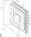
- Fig. 1 shows a bird's-eye view configuration of a power module 20 according to the embodiments.
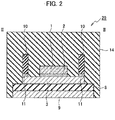
- Fig. 2 shows a schematic cross-sectional structure of a principal portion taken in line II-II of Fig. 1 in which a ceramic frame (frame member) 10 is disposed at a peripheral portion of a metallic pattern (metallic substrate) 3 formed on a ceramics substrate (mounting substrate) 8, in the power module 20 according to the embodiments.
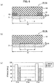
- Fig. 3(a) shows a planar pattern configuration of the ceramic frame 10 disposed at a peripheral portion of the metallic pattern 3 on the ceramics substrate 8
- Fig. 3 (b) shows a schematic cross-sectional structure taken in the line IIIb-IIIb of Fig. 3(a) .
- the principal portion of the power module 20 includes: a ceramics substrate 8; a semiconductor device (semiconductor chip) 1 as a power device configured to be bonded near a center portion of the metallic pattern 3 on the ceramics substrate 8; a ceramic frame 10 disposed along an edge of the metallic pattern 3 on the ceramics substrate 8, a cross-sectional structure of the ceramic frame 10 configured to enclose the semiconductor device 1 being an I-shaped structure; and a resin layer 14 configured to seal the semiconductor device 1 and the ceramics substrate 8 so as to include the ceramic frame 10.
- the semiconductor device 1 is illustrated as one element, it may be composed of a plurality of elements (e.g., modules).
- the semiconductor device 1 is bonded with solder on an upper surface of the metallic pattern 3 via a bonding layer under chip (bonded portion) 2, and the ceramic frame 10 is bonded with solder on the upper surface of the metallic pattern 3 via a bonding layer under frame 11 capable of solder bonding by being subjected to metal sputtering etc.
- the resin layer 14 configured to cover side surface portions of the ceramics substrate 8 is formed using a resin, etc. , capable of transfer molding.
- DBC Direct Bonding Copper
- DBA Direct Brazed Aluminum
- AMB Active Metal Brazed, Active Metal Bond
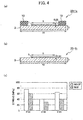
- Figs. 4(a)-4(c) respectively show stresses applied to the bonded portion between the semiconductor device 1 and the metallic pattern 3, comparing between a case of being provided with the ceramic frame 10 (WCF: With Ceramic Frame) and a case of being provided without the ceramic frame 10 (WOCF: Without Ceramic Frame), when no resin layer 14 is formed thereon.
- Fig. 4 (a) shows a schematic cross-sectional structure of a power module 20-1a in the case of being provided with the ceramic frame 10
- Fig. 4(b) shows a schematic cross-sectional structure of a power module 20-1b in the case of being provided without the ceramic frame 10
- Fig. 4(c) graphically shows each component ( ⁇ xx, ⁇ zz, ⁇ zx) of a simulation result of each stress.
- a size (width ⁇ thickness) of a cross section of the metallic pattern 3 is set as 10 ⁇ 1
- a size (width ⁇ thickness) in a cross-sectional direction of the semiconductor device 1 is set as 5 ⁇ 0.25.
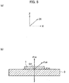
- a component in the direction z of a stress applied to the bonded portion CP is referred to as the vertical stress ⁇ zz
- a component in the direction x of the stress applied to the bonded portion CP is referred to as the horizontal stress ⁇ xx
- a component in the direction zx of the stress applied to the bonded portion CP is referred to as the shear stress ⁇ zx, as shown in Figs. 5(a) and 5(b) .
- the shear stress ⁇ zx can be reduced more remarkably than other stresses ⁇ xx and ⁇ zz.
- Figs. 6(a)-6(c) respectively show stresses applied to the bonded portion between the semiconductor device 1 and the metallic pattern 3, comparing between a case of being provided with the ceramic frame 10 (WCF) and a case of being provided without the ceramic frame 10 (WOCF), when the resin layer 14 is formed thereon.
- Fig. 6(a) shows a schematic cross-sectional structure of a power module 20-2a in the case of being provided with the ceramic frame 10
- Fig. 6(b) shows a schematic cross-sectional structure of a power module 20-2b in the case of being provided without the ceramic frame 10
- Fig. 6(c) graphically shows each component ( ⁇ xx, ⁇ zz, ⁇ zx) of a simulation result of each stress.
- the shear stress ⁇ zx can be reduced more remarkably than other stresses ⁇ xx and ⁇ zz.
- Figs. 7-10 show the operation/working-effect produced by being providing the ceramic frame 10 in order to be further explained in detail, in the power module 20 according to the embodiments.
- Figs. 7 and 8 respectively show stresses applied to the bonded portion between the semiconductor device (SiC) 1 and the metallic pattern (Cu substrate) 3, comparing between a case of being provided with the ceramic frame (SiN) 10 and a case of being provided without the ceramic frame (SiN) 10, when the resin layer (Resin) 14 is not formed thereon.
- Fig. 7(a) shows a schematic cross-sectional structure of the power module 20-1a in the case of being provided with the ceramic frame 10 axisymmetrically taken in the line Yc-Yc
- Fig. 7(b) shows a schematic cross-sectional structure of the power module 20-1b in the case of being provided without the ceramic frame 10 axisymmetrically taken in the line Yc-Yc.
- Fig. 7(a) shows a schematic cross-sectional structure of the power module 20-1a in the case of being provided with the ceramic frame 10 axisymmetrically taken in the line Yc-Yc
- Fig. 7(b) shows a schematic cross-section
- FIG. 8(a) shows a stress simulation result showing a relationship between a distance from the axis of the power module 20-1a and a shear stress ⁇ zx
- Fig. 8(b) shows a stress simulation result showing a relationship between a distance from the axis of the power module 20-1b and a shear stress ⁇ zx.
- the thickness of the cross section of the ceramic frame 10 is thicker than the thickness of the semiconductor device 1, and the size (width ⁇ thickness) of the cross section of the ceramic frame 10 is set to 2 ⁇ 1 (the approximately same thickness as the metallic pattern 3), for example.
- Figs. 9 and 10 respectively show stresses applied to the bonded portion between the semiconductor device (SiC) 1 and the metallic pattern (Cu substrate) 3, comparing between a case of being provided with the ceramic frame (SiN) 10 and a case of being provided without the ceramic frame (SiN) 10, when the resin layer (Resin) 14 is formed thereon.
- Fig. 9(a) shows a schematic cross-sectional structure of the power module 20-2a in the case of being provided with the ceramic frame 10 axisymmetrically taken in the line Yc-Yc
- Fig. 9(b) shows a schematic cross-sectional structure of the power module 20-2b in the case of being provided without the ceramic frame 10 axisymmetrically taken in the line Yc-Yc.
- Fig. 9(a) shows a schematic cross-sectional structure of the power module 20-2a in the case of being provided with the ceramic frame 10 axisymmetrically taken in the line Yc-Yc
- Fig. 9(b) shows a schematic cross-sectional
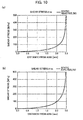
- FIG. 10(a) shows a stress simulation result showing a relationship between a distance from the axis of the power module 20-2a and a shear stress ⁇ zx
- Fig. 10(b) shows a stress simulation result showing a relationship between a distance from the axis of the power module 20-2b and a shear stress ⁇ zx.
- the size (width ⁇ thickness) of the cross section of the resin layer 14 is set to 15 ⁇ 7.5.
- the ceramic frame 10 has a function of suppressing the shear stress ⁇ zx according to the difference between the CTE value of the metallic pattern 3 and the CTE value of the semiconductor device 1. More specifically, the ceramic frame 10 has an effect of reducing the CTE value of Cu so that the metallic pattern 3 is not shrunk.
- the shear stress ⁇ zx applied to the bonded portion CP at the time of the heat cycle test, etc. can be remarkably reduced by providing the ceramic frame 10 having the CTE value smaller than the CTE value of Cu of the metallic pattern 3 but larger than the CTE value of the semiconductor device 1, as described above.
- the ceramic frame (SiN) 10 having the CTE value of approximately 2-10 ppm/K may be provided, in the power module 20 according to the embodiments.
- the CTE value of the resin layer 14 is set as approximately 12-14 ppm/K, in the power module 20 according to the embodiments.
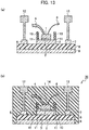
- a fabrication method of the power module 20 mainly includes: forming a ceramic frame 10 on a peripheral portion of a metallic pattern 3 on a ceramics substrate 8; disposing a semiconductor device 1 on the metallic pattern 3 inside the ceramic frame 10; and forming a resin layer 14 configured to seal the semiconductor device 1 and the ceramics substrate 8 so as to include the ceramic frame 10.
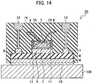
- the power module 20 includes a heat sink 100 as shown in Fig. 14 , for example, and the ceramics substrate 8 may be disposed on the heat sink 100.
- the heat sink 100 is formed by including a Cu base for heat radiation, for example.
- the metallic pattern 9 formed on the back side surface of the ceramics substrate 8 is connected to the heat sink 100 via a soldering layer 16 under substrate.
- a simplification of the module fabrication process and a miniaturization of the module can be realized since the module fabrication can be realized without attachment of a case.
- a height of the ceramic frame 10 is approximately 5 mm to approximately 0.2 mm, for example. Moreover, the ceramic frame 10 is formed in an approximately square shape. The height and width of the frame are preferable to be made as small as possible so that the chip size is suitable for the purpose of a miniaturization and a cost reduction, in the light of a sufficiently effective design calculated from the simulation result etc.
- the ceramics may be formed by including: Al 2 O 3 , AlN, SiN, AlSiC; or SiC of which at least the front side surface has insulating property, for example.
- a front side surface of Al 2 O 3 may be subjected to plating processing of W, Ni, the Au, or the like.
- the frame member may be formed by milling etc.
- a thickness of the resin layer 14 is approximately 4.0 mm to approximately 10 mm, for example.
- the block terminal electrodes 12 and 13 may be formed by including Cu, CuMo, or the like.
- the ceramic substrate 8 may be formed by including: Al 2 O 3 , AlN, SiN, AlSiC; or SiC of which at least the front side surface has insulating property, for example.
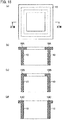
- Fig. 15 (a) shows a planar pattern configuration of a ceramic frame 10, in the power module according to a modified example 1 of the embodiments
- Fig. 15(b) shows a schematic cross-sectional structure taken in the line XVII-XVII of Fig. 15(a) .
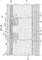
- a cross-sectional structure of the ceramic frame 10 may have a T-shaped structure by being provided with a ceramic frame 10 including a cap portion 10A of a protruding structure, as shown in Fig. 15(b) .
- An engaging degree of the resin layer 14 can be improved and thereby adhesibility thereof can be improved, by being provided with the ceramic frame 10 including the cap portion 10A of the protruding structure.
- Fig. 15(c) shows a schematic cross-sectional structure of a ceramic frame 10, in a power module according to a modified example 2 of the embodiments.
- a cross-sectional structure of the ceramic frame 10 may have an inverted-L-shaped structure or ⁇ (gamma)-shaped structure by being provided with a cap portion 10B, as shown in Fig. 15(c) .
- An engaging degree of the resin layer 14 can be improved and thereby adhesibility thereof can be improved, by being provided with the ceramic frame 10 including the cap portion 10B of the protruding structure.
- Fig. 15(d) shows a schematic cross-sectional structure of a ceramic frame 10, in a power module according to a modified example 3 of the embodiments.
- a cross-sectional structure of the ceramic frame 10 may have an inverted-L-shaped structure or ⁇ -shaped structure by being provided with a cap portion 10C, as shown in Fig. 15(d) .
- An engaging degree of the resin layer 14 can be improved and thereby adhesibility thereof can be improved, by being provided with the ceramic frame 10 including the cap portion 10C of the protruding structure.
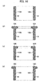
- Fig. 16(a) shows a schematic cross-sectional structure of a ceramic frame 10, in a power module according to a modified example 4 of the embodiments.
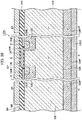
- a surface roughening process may be applied to a surface 10S of a ceramic frame 10 having an I-shaped structure.
- the surface roughening process to be applied to the ceramic frame 10 can be realized by a sandblast processing etc.
- an engaging degree of the resin layer 14 can be further improved and thereby adhesibility thereof can be improved, by applying the surface roughening process to the surface 10S of the ceramic frame 10.
- Fig. 16(b) shows a schematic cross-sectional structure of a ceramic frame 10, in a power module according to a modified example 5 of the embodiments.
- a surface roughening process may be applied to a surface 10S of a ceramic frame 10 having a T-shaped structure, by being provided with the cap portion 10A.
- an engaging degree of the resin layer 14 can be further improved and thereby adhesibility thereof can be improved, by applying the surface roughening process to the surface 10S of the ceramic frame 10.
- Fig. 16(c) shows a schematic cross-sectional structure of a ceramic frame 10, in a power module according to a modified example 6 of the embodiments.
- a surface roughening process may be applied to a surface 10S of a ceramic frame 10 having an inverted-L-shaped structure or ⁇ -shaped structure, by being provided with the cap portion 10B.
- an engaging degree of the resin layer 14 can be further improved and thereby adhesibility thereof can be improved, by applying the surface roughening process to the surface 10S of the ceramic frame 10.
- Fig. 16(d) shows a schematic cross-sectional structure of a ceramic frame 10, in a power module according to a modified example 7 of the embodiments.
- a surface roughening process may be applied to a surface 10S of a ceramic frame 10 having an inverted-L-shaped structure or ⁇ -shaped structure, by being provided with the cap portion 10C.
- an engaging degree of the resin layer 14 can be further improved and thereby adhesibility thereof can be improved, by applying the surface roughening process to the surface 10S of the ceramic frame 10.
- Figs. 17(a)-17(d) show planar pattern configurations of ceramic frames 10, in a power module according to a modified example 8 of the embodiments.
- a ceramic frame 10a of rectangular shape, e.g. rectangle, may be adopted, as shown in Fig. 17(a) .
- the ceramic frame is not limited to the ceramic frame 10a enclosing the periphery of one semiconductor device 1, but a ceramic frame 10b enclosing the periphery of a plurality of semiconductor devices 1A and 1B as shown in Fig. 17(b) may be adopted.
- a circle-shaped (e.g. circular or elliptical) ceramic frame 10c maybe adopted, as shown in Fig. 17(c) .
- a line-shaped (e.g. straight line-shaped) ceramic frame 10d disposed along a long side of the metallic pattern 3 near the semiconductor devices 1A and 1B, without enclosing the periphery of semiconductor devices 1A and 1B, may be adopted, as shown in Fig. 17(d) .
- the ceramic frame 10 is not limited to a structure of being arranged along an edge of the metallic pattern 3, but the ceramic frame 10 may be arranged at an inner side of the edge of the metallic pattern 3 as shown in Figs. 17(a)-17(d) .
- each of the ceramic frames 10a-10d respectively shown in Figs. 17(a)-17(d) may not always be integral-type frame, but may be divided to be fragmentarily arranged.
- the power module according to the embodiments and its modified examples can be applied, in particular to various transfer-mold type power modules, e.g. IGBT modules in which IGBT chips are mounted on metallic (e.g. Cu) substrates, diode modules, MIS (Si, SiC, GaN) modules.
- IGBT modules in which IGBT chips are mounted on metallic (e.g. Cu) substrates, diode modules, MIS (Si, SiC, GaN) modules.
- the low-cost power module having a simplified structure, easy to be fabricated through a simplified and easy process, and capable of improving mass productivity and realizing miniaturization thereof.
- the power module can be easily fabricated and excellent also in mass productivity.
- a block terminal electrode 17 may be provided therein, instead of the bonding wires 4 and 6.
- the block terminal electrode 17 can be disposed on a gate electrode or source electrode on the front side surface of the semiconductor device 1. Although one block terminal electrode 17 is illustrated in an example shown in Fig. 18 , a plurality of the block terminal electrodes 17 may be disposed for the gate and source electrodes. Moreover, the block terminal electrode 17 may be formed by including Cu, CuMo, or the like.
- the power module 20 may include: a relaying substrate 18 configured to select a bonding wire 19 and a block terminal electrode 23, relaying substrate 18 disposed on the metallic pattern 3 inside the ceramic frame 10; and a block terminal electrode 21 configured to connect between a source electrode on the semiconductor device 1 and a metallic pattern 7 on the ceramics substrate 8.
- Fig. 19 shows a schematic cross-sectional structure of the power module 20
- Fig. 20 shows a bird's-eye view configuration of the power module 20 such that the resin layer 14 is in a transmitted state.
- the relaying substrate 18 includes a ceramics substrate, and copper foils (Cu frames) formed respectively on front side and back side surfaces of the ceramics substrate. More specifically, the relaying substrate 18 has a DBC substrate structure. Moreover, a DBA substrate or AMB substrate may be used as the relaying substrate 18.
- the bonding wire 19 bonding-connects between the gate electrode on the semiconductor device 1 and the copper foil on the relaying substrate 18.
- the bonding wire 19 can be formed by including Al, AlCu, or the like, for example.
- the block terminal electrode 23 is configured to connect between the copper foil on the relaying substrate 18 and the metallic pattern 5 on the ceramics substrate 8 respectively via soldering layers (not shown).
- the block terminal electrodes 21 and 23 may be formed by including Cu, CuMo, or the like.
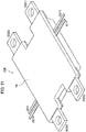
- Fig. 21 shows a bird's-eye view configuration of so-called 2-in-1 module (module with the built-in half-bridge) in which two semiconductor devices are contained in one module, in a power module 200 according to an additional embodiment 3.
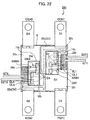
- Fig.22 shows a planar pattern configuration of the power module 200 before forming the resin layer 14
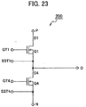
- Fig. 23 shows a circuit configuration of the 2-in-1 module to which SiC MISFETs Q1 and Q4 are applied as semiconductor devices.
- the power module 200 includes a configuration of a module with so-called built-in half-bridge in which two MISFETs Q1 and Q4 are built in one module.
- Fig. 22 shows an example of 4-chip of the MISFETs Q1 and 4-chip of the MISFETs Q4 respectively disposed in parallel.
- one MISFET can mount five transistors (chip) at the maximum. Note that it is also possible to mount a part of five pieces of the chips for the diode DI thereon.
- the module can be understood as one large transistor, one piece or a plurality of transistors (chips) may be contained therein. More specifically, although the modules include 1-in-1 module, 2-in-1 module, 4-in-1 module, 6-in-1 module, etc., for example, a module configured to vertically connect two transistors to be contained on the module is called 2-in-1 module, a module configured to wire 2 sets of 2-in-1 module to be contained on the module is called 4-in-1 module, and a module configured to wire all to be contained on the module is called 6-in-1 module.
- the power module 200 includes: a positive-side power terminal P (D1) and a negative-side power terminal N (S4) disposed at a first side of the ceramic substrate 8 covered with the resin layer 14; a gate terminal GT1 and a source sense terminal SST1 disposed at a second side adjacent to the first side; output terminals O (S1) and O (D1) disposed at a third side opposite to the first side; and a gate terminal GT4 and a source sense terminal SST4 disposed at a fourth side opposite to the second side.
- the gate terminal GT1 and the source sense terminal SST1 are connected to the signal wiring pattern GL1 for gate and the signal wiring pattern SL1 for source in the MISFET Q1; and the gate terminal GT4 and the source sense terminal SST4 are connected to the signal wiring pattern GL4 for gate and the signal wiring pattern SL4 for source in the MISFET Q4.
- wires for gate GW1 and GW4 and wires for source sense SSW1 and SSW4 are respectively connected from the MISFETs Q1 and Q4 toward the gate signal wiring patterns GL1 and GL4 and the source sense signal wiring patterns SL1 and SL4 which are respectively disposed on the signal substrates 24 1 and 24 4 .
- gate terminals GT1 and GT4 and source sense terminals SST1 and SST4 for external extraction are respectively connected to the signal wiring patterns GL1 and GL4 for gate and the signal wiring patterns SL1 and SL4 for source sense by soldering etc.
- the signal substrates 24 1 and 24 4 are connected by soldering etc. on the ceramics substrate 8.
- Fig. 24 shows a bird' s-eye view configuration before forming the resin layer 14 after forming upper surface plate electrodes 22 1 and 22 4 , in the module with the built-in half-bridge, in the power module 200 according to the additional embodiment 3. Note that the wires GW1 and GW4 for gate and the wires SSW1 and SSW4 for source sense are not shown in Fig. 24 .
- the sources S1 and S4 of 4 chips of the MISFETs Q1 and Q4 respectively disposed in parallel are commonly connected with the upper surface plate electrodes 22 1 and 22 4 .
- diodes may be respectively connected reversely in parallel between a drain D1 and a source S1 and between a drain D4 and a source S4 of the MISFETs Q1 and Q4.
- the sources S1 and S4 of 4 chips of the MISFETs Q1 and Q4 disposed in parallel are commonly connected with the upper surface plate electrodes 22 1 and 22 4 in an example shown in Figs. 21-24 , the sources may be conducted to one another with the wire instead of the upper surface plate electrodes 22 1 and 22 4 .
- the positive-side power terminal P and the negative-side power terminal N, and the gate terminals GT1 and GT4 and the source sense terminals SST1 and SST4 for external extraction can be formed of Cu, for example.
- the signal substrates 241 and 244 can be formed by including a ceramics substrate.
- the ceramic substrate may be formed by including Al 2 O 3 , AlN, SiN, AlSiC, or SiC of which at least the surface is insulation, for example.
- Main wiring conductors (metallic substrates) 32 1 , 32 4 , and 32 n (EP) used for electrode patterns can be formed by including Cu, Al, or the like, for example.
- Portions of pillar electrodes 25 1 and 25 4 and upper surface plate electrodes 22 1 and 22 4 configured to respectively connect between the sources S1 and S4 of the MISFETs Q1 and Q4 and the upper surface plate electrodes 22 1 and 22 4 may be formed by including CuMo, Cu, or the like, for example.
- the wires GW1 and GW4 for gate and the wires SSW1 and SSW4 for source sense can be formed by including Al, AlCu, or the like, for example.
- Wide-bandgap type elements such as SiC based power devices (e.g. SiC DIMISFET and SiC TMISFET), or GaN based power devices (e.g. GaN based FET, High Electron Mobility Transistor (HEMT)), can be applied as the MISFETs Q1 and Q4.
- SiC based power devices e.g. SiC DIMISFET and SiC TMISFET
- GaN based power devices e.g. GaN based FET, High Electron Mobility Transistor (HEMT)
- HEMT High Electron Mobility Transistor
- power devices e.g. Si based MISFETs and IGBT, are also applicable thereto.
- 4 chips of the MISFETs Q1 are bonded via a bonding layer 2 under chip on the main wiring conductor 32 1 in the ceramic frame 10 1 disposed via a soldering layer etc. on the main wiring conductor 32 1 .
- 4 chips of the MISFETs Q4 are bonded via a bonding layer 2 under chip on the main wiring conductor 32 4 in the ceramic frame 10 4 disposed via a soldering layer etc. on the main wiring conductor 32 4 .
- each of the ceramic frames 10 1 and 10 4 is filled up with a resin, and each of the 4 chips of the MISFETs Q1 and Q4 is sealed with the resin. Moreover, the whole module is packaged by the resin layer 14 so as to include the upper surface plate electrodes 22 1 and 22 4 , etc. The whole of the resin layer 14 is formed of a homogeneous material.
- respective ceramic frames 10 1 and 10 4 are configured to collectively contain the respective MISFETs Q1 and Q4, in the example shown in Figs. 22 and 24 , but the respective ceramic frames 10 1 and 10 4 may be configured to individually contain the respective MISFETs Q1 and Q4.
- the principal portion of the power module 200 according to the additional embodiment 3 includes: a ceramics substrate 8; MISFETs Q1 and Q4 respectively bonded to main wiring conductors 32 1 and 32 4 on the ceramics substrate 8; ceramic frames 10 1 and 10 4 respectively disposed on the main wiring conductor 32 1 and 32 4 , the ceramic frames 10 1 and 10 4 configured to enclose the MISFETs Q1 and Q4; and resin layers 14 configured to respectively seal the MISFETs Q1 and Q4 inside the ceramic frames 10 1 and 10 4 , and to respectively seal the main wiring conductors 32 1 and 32 4 and the ceramics substrate 8 inside the ceramic frames 10 1 and 10 4 .
- the same resin material as that of the embodiments and its modified examples 1-8 can be applied to the resin layer 14, and the same configuration of the ceramic frame 10 as that of the embodiments and its modified examples 1-8 can be adopted into the ceramic frames 10 1 and 10 4 .
- the block terminal electrodes 12 and 13, the relaying substrate 18, etc. may be applied instead of the wires GW1 and GW4 for gate and the wires SSW1 and SSW4 for source sense, in order to prevent wire breaking due to a thermal stress etc. and to obtain an improvement in reliability.
- a simplification of the module fabrication process and a miniaturization of the module can be realized since the same fabrication method as that of the embodiments or other additional embodiments can be applied and therefore the module fabrication can be realized without attachment of a case. Also in the power module 200 according to the additional embodiment 3, since structural members, e.g. a case, are unnecessary, the number of parts is reduced, and thereby realizing cost reduction.
- the low-cost power module having a simplified structure, easy to be fabricated through a simplified and easy process, and capable of improving mass productivity and realizing miniaturization thereof.
- the power module can be easily fabricated and excellent also in mass productivity.
- the power module 20 according to the embodiments.
- the configuration in which the ceramic frame 10 is formed in the periphery of the semiconductor device 1 on the metallic pattern 3 is adopted, in order to reduce the difference between the CTE value of the metallic pattern 3 and the CTE value of the semiconductor device 1 also in the power module 20 explained hereinafter.
- Fig. 25(a) shows a schematic circuit representative of an SiC MISFET of the 1-in-1 module, which is the power module 20 according to the embodiments.
- Fig. 25(b) shows a schematic circuit representation of the IGBT of the 1-in-1 module.
- a diode DI connected in reversely parallel to the MISFET Q is shown in Fig. 25(a) .
- a main electrode of the MISFET Q is expressed with a drain terminal DT and a source terminal ST.
- a diode DI connected in reversely parallel to the IGBT Q is shown in Fig. 25(b) .
- a main electrode of the IGBT Q is expressed with a collector terminal CT and an emitter terminal ET.
- Fig. 26 shows a detailed circuit representative of the SiC MISFET of the 1-in-1 module, which is the power module 20 according to the embodiments.
- the power module 20 includes a configuration of 1-in-1 module, for example. More specifically, one MISFET is contained in one module, and a maximum of 5 chips (five transistors) connected in parallel to one another can be mounted in one MISFET, as an example . Note that it is also possible to mount a part of five pieces of the chips for the diode DI thereon.
- a sense MISFET Qs is connected to the MISFETQ in parallel.
- the sense MISFET Qs is formed as a miniaturized transistor in the same chip as the MISFET Q.
- reference numeral SS denotes a source sense terminal
- reference numeral CS denotes a current sense terminal
- reference numeral G denotes a gate signal terminal.
- the sense MISFET Qs is formed as a miniaturized transistor in the same chip.
- Fig. 27(a) shows a circuit representative of the SiC MISFET of the 1-in-1 module, which is the power module 20T according to the embodiments.
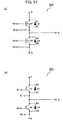
- FIG. 27(a) two MISFETs Q1 and Q4, and diodes D1 and D4 connected in reversely parallel to the MISFETs Q1 and Q4 are built in one module.
- reference numeral G1 denotes a gate signal terminal of the MISFET Q1
- reference numeral S1 denotes a source terminal of the MISFET Q1.
- Reference numeral G4 denotes a gate signal terminal of the MISFET Q4, and reference numeral S4 denotes a source terminal of the MISFET Q4.
- Reference numeral P denotes a positive side power input terminal
- reference numeral N denotes a negative side power input terminal
- reference numeral O denotes an output terminal.
- Fig. 27 (b) shows a circuit representative of the 2-in-1 module, which is the power module 20T according to the embodiments.
- FIG. 27 (b) two IGBTs Q1 and Q4, and diodes D1 and D4 connected in reversely parallel to the IGBTs Q1 and Q4 are built in one module.
- reference numeral G1 denotes a gate signal terminal of the IGBT Q1
- reference numeral E1 denotes an emitter terminal of the IGBT Q1.
- Reference numeral G4 denotes a gate signal terminal of the IGBT Q4, and reference numeral E4 denotes an emitter terminal of the IGBT Q4.
- Reference numeral P denotes a positive side power input terminal
- reference numeral N denotes a negative side power input terminal
- reference numeral O denotes an output terminal.
- Fig. 28(a) shows a schematic cross-sectional structure of an SiC MISFET 110, which is an example of a semiconductor device which can be applied to the power modules 20 and 20T according to the embodiments
- Fig. 28(b) shows a schematic cross-sectional structure of the IGBT 110A.
- the schematic cross-sectional structure of the SiC MISFET 110 includes: a semiconductor substrate 126 composed by including an n - type high resistivity layer; a p body region 128 formed on a front surface side of the semiconductor substrate 126; a source region 130 formed on a front side surface of the p body region 128; a gate insulating film 132 disposed on a front side surface of the semiconductor substrate 126 between the p body regions 128; a gate electrode 138 disposed on the gate insulating film 132; a source electrode 134 connected to the source region 130 and the p body region 128; an n + drain region 124 disposed on a back side surface opposite to the surface of the semiconductor substrate 126; and a drain electrode 136 connected to the n + type drain area 124.
- the semiconductor device may be composed by including a trench-gate-type n channel vertical SiC-TMISFET, etc., shown in Fig. 32 mentioned below.
- a GaN based FET etc. can also be adopted thereinto, instead of the SiC MISFET. It is especially effective to adopt any one of an SiC-based or GaN-based power device, as the power modules 20 and 20T according to the embodiments.
- a wide-bandgap type semiconductor of which the bandgap energy is from 1.1 eV to 8 eV, for example, can be used for the semiconductor device applicable to the power modules 20 and 20T according to the embodiments.
- IGBT 110A as an example of the semiconductor device applicable to the power modules 20 and 20T according to the embodiments includes: a semiconductor substrate 126 composed by including an n - type high resistivity layer; a p body region 128 formed on a front surface side of the semiconductor substrate 126; an emitter region 130E formed on a front side surface of the p body region 128; a gate insulating film 132 disposed on a front side surface of the semiconductor substrate 126 between the p body regions 128; a gate electrode 138 disposed on the gate insulating film 132; an emitter electrode 134E connected to the emitter region 130E and the p body region 128; a p + collector region 124P disposed on a back side surface opposite to the surface of the semiconductor substrate 126; and a collector electrode 136 connected to the p + collector region 124P.
- the semiconductor device 110 composed by including the planar-gate-type n channel vertical IGBT is disclosed, the semiconductor device may be composed by including a trench-gate-type n channel vertical IGBT, etc.
- Fig. 29 shows a schematic cross-sectional structure of an SiC MISFET 110 including a source pad electrode SP and a gate pad electrode GP, which is an example of the semiconductor device applicable to the power modules 20 and 20T according to the embodiments.
- the gate pad electrode GP is connected to the gate electrode 138 disposed on the gate insulating film 132, and the source pad electrode SP is connected to the source electrode 134 connected to the source region 130 and the p body region 128. Moreover, as shown in Fig. 29 , the gate pad electrode GP and the source pad electrode SP are disposed on an interlayer insulating film 144 for passivation which covers the surface thereof.
- microstructural transistor structure may be formed in the semiconductor substrate 126 below the gate pad electrode GP and the source pad electrode SP in the same manner as the center portion shown in Fig. 28(a) or 29 .
- the source pad electrode SP may be disposed to be extended onto the interlayer insulating film 144 for passivation, also in the transistor structure of the center portion.
- Fig. 30 shows a schematic cross-sectional structure of an IGBT 110A including a source pad electrode SP and a gate pad electrode GP, which is an example of the semiconductor device applied to the power modules 20 and 20T according to the embodiments.
- the gate pad electrode GP is connected to the gate electrode 138 disposed on the gate insulating film 132, and the emitter pad electrode EP is connected to the emitter electrode 134E connected to the emitter region 130E and the p body region 128. Moreover, as shown in Fig. 30 , the gate pad electrode GP and the emitter pad electrode EP are disposed on an interlayer insulating film 144 for passivation which covers the surface thereof.
- microstructural IGBT structure may be formed in the semiconductor substrate 126 below the gate pad electrode GP and the emitter pad electrode EP in the same manner as the center portion shown in Fig. 28(b) or 30 .
- the emitter pad electrode EP may be disposed to be extended onto the interlayer insulating film 144 for passivation, also in the IGBT structure of the center portion.
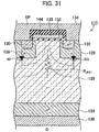
- Fig. 31 shows a schematic cross-sectional structure of an SiC DIMISFET 110, which is an example of a semiconductor device which can be applied to the power module 20T according to the embodiments.
- the SiC DIMISFET applicable to the power module 20T includes: a semiconductor substrate 126 composed by including an n - type high resistivity layer; a p body region 128 formed on a front surface side of the semiconductor substrate 126; an n + source region 130 formed on a front side surface of the p body region 128; a gate insulating film 132 disposed on a front side surface of the semiconductor substrate 126 between the p body regions 128; a gate electrode 138 disposed on the gate insulating film 132; a source electrode 134 connected to the source region 130 and the p body region 128; an n + drain region 124 disposed on a back side surface opposite to the surface of the semiconductor substrate 126; and a drain electrode 136 connected to the n + type drain area 124.
- the p body region 128 and the n + source region 130 formed on the front side surface of the p body region 128 are formed with double ion implantation (DI), and the source pad electrode SP is connected to the source region 130 and the source electrode 134 connected to the p body region 128.
- a gate pad electrode GP (not shown) is connected to the gate electrode 138 disposed on the gate insulating film 132.
- the source pad electrode SP and the gate pad electrode GP are disposed on an interlayer insulating film 144 for passivation configured to cover the front side surface thereof.
- a depletion layer as shown with the dashed lines is formed in the semiconductor substrate 126 composed of a n - type high resistivity layer inserted into the p body regions 128, channel resistance RJ FET accompanying the junction type FET (JFET) effect is formed.
- body diodes BD are respectively formed between the p body regions 128 and the semiconductor substrates 126.
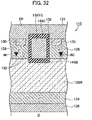
- Fig. 32 shows a schematic cross-sectional structure of an SiC TMISFET 110, which is an example of a semiconductor device which can be applied to the power module 20T according to the embodiments.
- the SiC TMISFET applicable to the power circuit 20T includes: a semiconductor substrate 126N composed by including an n layer; a p body region 128 formed on a front surface side of the semiconductor substrate 126N; an n + source region 130 formed on a front side surface of the p body region 128; a trench gate electrode 138TG passing through the p body region 128, the trench gate electrode 138TG formed in the trench formed up to the semiconductor substrate 126N via the gate insulating layer 132 and the interlayer insulating films 144U and 144B; a source electrode 134 connected to the source region 130 and the p body region 128; an n + type drain area 124 disposed on a back side surface of the semiconductor substrate 126N opposite to the front side surface thereof; and a drain electrode 136 connected to the n + type drain area 124.
- a trench gate electrode 138TG passing through the p body region 128 is formed in the trench formed up to the semiconductor substrate 126N via the gate insulating layer 132 and the interlayer insulating films 144U and 144B; and the source pad electrode SP is connected to the source region 130 and the source electrode 134 connected to the p body region 128.
- a gate pad electrode GP (not shown) is connected to the gate electrode 138 disposed on the gate insulating film 132.
- the source pad electrode SP and the gate pad electrode GP are disposed on an interlayer insulating film 144U for passivation configured to cover the front side surface thereof.
- channel resistance RJ FET accompanying the junction type FET (JFET) effect as the SiC DIMISFET is not formed.
- body diodes BD are respectively formed between the p body regions 128 and the semiconductor substrates 126N, in the same manner as Fig. 31 .
- Fig. 33(a) shows an example of a circuit configuration in which the SiC MISFET is applied as a semiconductor device, and a snubber capacitor C is connected between the power terminal PL and the earth terminal (ground terminal) NL, in a circuit configuration of a three-phase AC inverter 140 composed using the power module 20T according to the embodiments.
- Fig. 33(b) shows an example of a circuit configuration in which the IGBT is applied as a semiconductor device, and a snubber capacitor C is connected between the power terminal PL and the earth terminal (ground terminal) NL, in a circuit configuration of a three-phase AC inverter 140A composed using the power module 20T according to the embodiments.
- the surge voltage Ldi/dt changes dependent on a value of the inductance L
- the surge voltage Ldi/dt is superimposed on the power source E.
- Such a surge voltage Ldi/dt can be absorbed by the snubber capacitor C connected between the power terminal PL and the earth terminal (ground terminal) NL.
- the three-phase AC inverter 140 includes a gate drive unit 150, a power module unit 152 connected to the gate drive unit 150, and a three-phase AC motor unit 154.
- U-phase, V-phase, and W-phase inverters are respectively connected to the three-phase AC motor unit 54 so as to correspond to U phase, V phase, and W phase of the three-phase AC motor unit 154, in the power module unit 152.
- the gate drive unit 150 is connected to the SiC MISFETs Q1 and Q4, SiC MISFETs Q2 and Q5, and the SiC MISFETs Q3 and Q6.
- the power module unit 152 includes the SiC MISFETs (Q1 and Q4), (Q2 and Q5), and (Q3 and Q6) having inverter configurations connected between a positive terminal (+) and a negative terminal (-) to which the converter 148 in a power supply or a storage battery (E) 146 is connected. Moreover, flywheel diodes D1-D6 are respectively connected reversely in parallel between the source and the drain of the SiC MISFETs Q1-Q6.
- the three-phase AC inverter 140A includes a gate drive unit 150A, a power module unit 152A connected to the gate drive unit 150A, and a three-phase AC motor unit 154A.
- U-phase, V-phase, and W-phase inverters are respectively connected to the three-phase AC motor unit 152A so as to correspond to U phase, V phase, and W phase of the three-phase AC motor unit 154A, in the power module unit 152A.
- the gate drive unit 150A is connected to the IGBTs Q1 and Q4, IGBTs Q2 and Q5, and the IGBTs Q3 and Q6.
- the power module unit 152A includes the IGBTs (Q1 and Q4), (Q2 and Q5), and (Q3 and Q6) having inverter configurations connected between a positive terminal (+) and a negative terminal (-) to which the converter 148A in a storage battery (E) 146A is connected. Moreover, flywheel diodes D1-D6 are respectively connected reversely in parallel between the emitter and the collector of the IGBTs Q1-Q6.
- the power module 20T can be formed as any one selected from the group consist of 1-in-1 module, 2-in-1 module, 4-in-1 module, 6-in-1 module, and 7-in-1 module.
- the power module easy to be fabricated, capable of suppressing the degradation of the bonded portion and improving reliability; and the inverter equipment on which such a power module is mounted, also when adopting the transfer-mold type power module.
- the embodiments cover a variety of embodiments and the like, whether described or not.
- the power module according to the embodiments can be used for manufacturing techniques for power modules, e.g. IGBT modules, diode modules, MIS modules (Si, SiC, GaN), and the like, and can be applied to wide applicable fields, e.g. inverters for HEV/EV, inverter and converters for industrial applications, etc.
Landscapes
- Engineering & Computer Science (AREA)
- Power Engineering (AREA)
- Cooling Or The Like Of Semiconductors Or Solid State Devices (AREA)
- Inverter Devices (AREA)
- Physics & Mathematics (AREA)
- Geometry (AREA)
- Chemical & Material Sciences (AREA)
- Materials Engineering (AREA)
Abstract
Description
- Embodiments described herein relate to a thermal resistance analysis model and a semiconductor integrated circuit.
- Many research institutions are currently conducting research to develop Silicon Carbide (SiC) devices. SiC power devices have low on resistance as compared with Si power devices, and also include high switching speed and high temperature operation characteristics.
- Since losses (on resistance) produced by SiC devices are relatively low, a large electric current can be conducted even in SiC power modules having small area and therefore such SiC power modules can be miniaturized.
- It is well known that case type packages are adopted into such SiC power devices, and resin sealed semiconductor devices are formed by transfer molding, as disclosed in the
Patent Literature 1. - In the light of miniaturization of conventional power modules, thin type power modules have been required therefor, and Direct Bonding Copper (DBC) substrates, Direct Brazed Aluminum (DBA) substrates, or Active Metal Brazed, Active Metal Bond (AMB) substrates have been used in mounting processes.
- Patent Literature 1: Japanese Patent Application Laying-Open Publication No.
2013-172044 - However, there is a problem that degradation (such as a rupture) of a bonded portion occurs during a heat cycle test, when semiconductor devices (e.g. SiC power devices) are bonded on metallic substrates (e.g. DBC substrates), if a difference between the both values of coefficient of thermal expansion (CTE) is relatively large.
- The embodiments provide: a power module easy to be fabricated, capable of suppressing such a degradation of the bonded portion and improving reliability; and the inverter equipment on which such a power module is mounted.
- According to one aspect of the embodiments, there is provided a ceramics substrate; a semiconductor device bonded near a center portion of a metallic pattern on the ceramics substrate; a ceramic frame disposed along an edge at a peripheral portion of the metallic pattern on the ceramics substrate, and configure to enclose the semiconductor device; a resin layer configured to seal the semiconductor device and the ceramics substrate so as to include the ceramic frame, wherein the ceramic frame suppresses a stress according to a difference between a coefficient of thermal expansion of the ceramics substrate and a coefficient of thermal expansion of the semiconductor device.
- According to another aspect of the embodiments, there is provided inverter equipment configured to mount at least one power module which is mentioned above as the switching elements.
- According to the embodiments, there can be provided: the power module easy to be fabricated, capable of suppressing the degradation of the bonded portion and improving reliability; and the inverter equipment on which such a power module is mounted.
-
- [
Fig. 1 ] A bird's-eye view configuration diagram (perspective diagram) showing a principal portion of a power module according to the embodiments. - [
Fig. 2 ] A schematic cross-sectional structure diagram taken in the line II-II ofFig. 1 . - [
Fig. 3 ] (a) A planar pattern configuration diagram showing a ceramic frame disposed on a metallic pattern, in the power module according to the embodiments, and (b) a schematic cross-sectional structure diagram taken in the line IIIb-IIIb ofFig. 3(a) . - [
Fig. 4 ] (a) A schematic cross-sectional structure diagram showing a power module with a ceramic frame, in an example of a case where no resin layer is formed thereon, (b) a schematic cross-sectional structure diagram showing a power module without a ceramic frame, in an example of a case where no resin layer is formed thereon, and (c) a simulation result showing a stress applied to the bonded portion being compared for each component. - [
Fig. 5 ] (a) A conceptual diagram showing the component in each direction of the stress, and (b) a schematic cross-sectional diagram for explaining each component of the stress applied to the bonded portion. - [
Fig. 6 ] (a) A schematic cross-sectional structure diagram showing a power module with a ceramic frame, in an example of a case where a resin layer is formed thereon, (b) a schematic cross-sectional structure diagram showing a power module without a ceramic frame, in an example of a case where a resin layer is formed thereon, and (c) a simulation result showing a stress applied to the bonded portion being compared for each component. - [
Fig. 7 ] (a) A schematic cross-sectional structure diagram axisymmetrically showing a power module with a ceramic frame, in an example of a case where no resin layer is formed thereon, and (b) a schematic cross-sectional structure diagram axisymmetrically showing a power module without a ceramic frame, in an example of a case where no resin layer is formed thereon. - [
Fig. 8 ] (a) A simulation result showing a relationship between a shear stress and a distance from an axis of the power module with a ceramic frame, in an example of a case where no resin layer is formed thereon, and (b) a simulation result showing a relationship between a shear stress and a distance from an axis of the power module without a ceramic frame, in an example of a case where no resin layer is formed thereon. - [
Fig. 9 ] (a) A schematic cross-sectional structure diagram axisymmetrically showing a power module with a ceramic frame, in an example of a case where a resin layer is formed thereon, and (b) a schematic cross-sectional structure diagram axisymmetrically showing a power module without a ceramic frame, in an example of a case where a resin layer is formed thereon. - [
Fig. 10 ] (a) A a simulation result showing a relationship between a shear stress and a distance from an axis of the power module with a ceramic frame, in an example of a case where a resin layer is formed thereon, and (b) a simulation result showing a relationship between a shear stress and a distance from an axis of the power module without a ceramic frame, in an example of a case where a resin layer is formed thereon. - [
Fig. 11 ] (a) A schematic cross-sectional structure diagram showing one process of a fabrication method of the power module according to the embodiments (Phase 1), and (b) a schematic cross-sectional structure diagram showing one process of the fabrication method of the power module according to the embodiments (Phase 2). - [
Fig. 12 ] (a) A schematic cross-sectional structure diagram showing one process of the fabrication method of the power module according to the embodiments (Phase 3), and (b) a schematic cross-sectional structure diagram showing one process of the fabrication method of the power module according to the embodiments (Phase 4). - [
Fig. 13 ] (a) A schematic cross-sectional structure diagram showing one process of the fabrication method of the power module according to the embodiments (Phase 5), and (b) a schematic cross-sectional structure diagram showing one process of the fabrication method of the power module according to the embodiments (Phase 6). - [
Fig. 14 ] A schematic cross-sectional structure diagram showing one process of the fabrication method of the power module according to the embodiments (Phase 7), in an example of a case where a heat sink is formed thereto. - [
Fig. 15 ] (a) A planar pattern configuration diagram showing a ceramic frame, in a power module according to a modified example 1 of the embodiments, (b) a schematic cross-sectional structure diagram taken in the line XVII-XVII ofFig. 15(a), (c) a schematic cross-sectional structure diagram showing a ceramic frame, in a power module according to a modified example 2 of the embodiments, and (d) a schematic cross-sectional structure diagram showing a ceramic frame, in a power module according to a modified example 3 of the embodiments. - [
Fig. 16 ] (a) A schematic cross-sectional structure diagram showing a ceramic frame, in a power module according to a modified example 4 of the embodiments, (b) a schematic cross-sectional structure diagram showing a ceramic frame, in a power module according to a modified example 5 of the embodiments, (c) a schematic cross-sectional structure diagram showing a ceramic frame, in a power module according to a modified example 6 of the embodiments, and (d) a schematic cross-sectional structure diagram showing a ceramic frame, in a power module according to a modified example 7 of the embodiments. - [
Fig. 17 ] (a) A planar pattern configuration diagram showing a ceramic frame in an example of a case where one semiconductor device is mounted therein (Phase 1-1), in a power module according to a modified example 8 of the embodiments, (b) a planar pattern configuration diagram showing a ceramic frame in an example of a case where two semiconductor devices are mounted therein (Phase 1-2), in the power module according to the modified example 8 of the embodiments, (c) a planar pattern configuration diagram showing a ceramic frame in an example of a case where one semiconductor device is mounted therein (Phase 2), in the power module according to the modified example 8 of the embodiments, and (d) a planar pattern configuration diagram showing a ceramic frame in an example of a case where two semiconductor devices are mounted therein (Phase 3), in the power module according to the modified example 8 of the embodiments. - [
Fig. 18 ] A schematic cross-sectional structure diagram showing a power module according to anadditional embodiment 1. - [
Fig. 19 ] A schematic cross-sectional structure diagram showing a power module according to anadditional embodiment 2. - [
Fig. 20 ] A bird's-eye view (perspective diagram) showing the power module according to theadditional embodiment 2 such that a resin layer is in a transmitted state. - [
Fig. 21 ] A bird's-eye view configuration diagram (perspective diagram) showing a module with the built-in half-bridge, in a power module according to anadditional embodiment 3. - [
Fig. 22 ] A planar pattern configuration diagram showing the power module according to theadditional embodiment 3 such that a resin layer is in a transmitted state, in a 2-in-1 module (module with the built-in half-bridge). - [
Fig. 23 ] A circuit configuration diagram showing the 2-in-1 module (module with the built-in half-bridge) in which an SiC Metal Oxide Semiconductor Field Effect Transistor (MISFET) is applied as a semiconductor device, in the power module according to theadditional embodiment 3. - [
Fig. 24 ] A bird's-eye view configuration diagram (perspective diagram) showing an aspect before forming the resin layer in the module with the built-in half-bridge, in the power module according to theadditional embodiment 3. - [
Fig. 25 ] (a) A circuit representative diagram of the SiC MISFET of a 1-in-1 module, which is the power module according to the embodiments, and (b) a circuit representative diagram of an Insulated Gate Bipolar Transistor (IGBT) of a 1-in-1 module, in the power module according to the embodiments. - [
Fig. 26 ] A detail circuit representative diagram of the SiC MISFET of the 1-in-1 module, which is the power module according to the embodiments. - [
Fig. 27 ] (a) A circuit representative diagram of an SiC MISFET of a 2-in-1 module, which is the power module according to the embodiments, and (b) a circuit representative diagram of an IGBT of a 2-in-1 module, which is the power module according to the embodiments. - [
Fig. 28 ] (a) A schematic cross-sectional structure diagram of an SiC MISFET, which is an example of a semiconductor device to be applied to the power module according to the embodiments, and (b) a schematic cross-sectional structure diagram of an IGBT, which is an example of the semiconductor device to be applied to the power module according to the embodiments. - [
Fig. 29 ] A schematic cross-sectional structure diagram showing an SiC MISFET including a source pad electrode SP and a gate pad electrode GP, which is an example of the semiconductor device to be applied to the power module according to the embodiments. - [
Fig. 30 ] A schematic cross-sectional structure diagram of the IGBT including an emitter pad electrode EP and a gate pad electrode GP, which is an example of the semiconductor device to be applied to the power module according to the embodiments. - [
Fig. 31 ] A schematic cross-sectional structure diagram of an SiC Double Implanted MISFET (SiC DIMISFET), which is an example of a semiconductor device which can be applied to the power module according to the embodiments. - [
Fig. 32 ] A schematic cross-sectional structure diagram of an SiC Trench MISFET (SiC TMISFET), which is an example of a semiconductor device which can be applied to the power module according to the embodiments. - [
Fig. 33 ] (a) An example of a circuit configuration in which the SiC MISFET is applied as a semiconductor device, and a snubber capacitor is connected between a power terminal PL and an earth terminal (ground terminal) NL, and (b) an example of a circuit configuration in which the IGBT is applied as a semiconductor device, and the snubber capacitor is connected between the power terminal PL and the earth terminal (ground terminal) NL, in the circuit configuration of a three-phase AC inverter composed using the power module according to the embodiments. - [
Fig. 34 ] A circuit configuration diagram of a three-phase AC inverter composed using the power module according to the embodiments to which the SiC MISFET is applied as the semiconductor device. - [
Fig. 35 ] A circuit configuration diagram of a three-phase AC inverter composed using the power module according to the embodiments to which the IGBT is applied as the semiconductor device. - Next, certain embodiments will now be described with reference to drawings. In the description of the following drawings, the identical or similar reference numeral is attached to the identical or similar part. However, it should be noted that the drawings are schematic and therefore the relation between thickness and the plane size and the ratio of the thickness differs from an actual thing. Therefore, detailed thickness and size should be determined in consideration of the following explanation.
- Moreover, the embodiments shown hereinafter exemplify the apparatus and method for materializing the technical idea; and the embodiments does not specify the material, shape, structure, placement, etc. of each component part as the following. The embodiments may be changed without departing from the spirit or scope of claims.
-
Fig. 1 shows a bird's-eye view configuration of apower module 20 according to the embodiments. Moreover,Fig. 2 shows a schematic cross-sectional structure of a principal portion taken in line II-II ofFig. 1 in which a ceramic frame (frame member) 10 is disposed at a peripheral portion of a metallic pattern (metallic substrate) 3 formed on a ceramics substrate (mounting substrate) 8, in thepower module 20 according to the embodiments. - Moreover, in the
power module 20 according to the embodiments,Fig. 3(a) shows a planar pattern configuration of theceramic frame 10 disposed at a peripheral portion of themetallic pattern 3 on theceramics substrate 8, andFig. 3 (b) shows a schematic cross-sectional structure taken in the line IIIb-IIIb ofFig. 3(a) . - As shown in
Figs. 1 and2 , the principal portion of thepower module 20 according to the embodiments includes: aceramics substrate 8; a semiconductor device (semiconductor chip) 1 as a power device configured to be bonded near a center portion of themetallic pattern 3 on theceramics substrate 8; aceramic frame 10 disposed along an edge of themetallic pattern 3 on theceramics substrate 8, a cross-sectional structure of theceramic frame 10 configured to enclose thesemiconductor device 1 being an I-shaped structure; and aresin layer 14 configured to seal thesemiconductor device 1 and theceramics substrate 8 so as to include theceramic frame 10. In each drawings, although thesemiconductor device 1 is illustrated as one element, it may be composed of a plurality of elements (e.g., modules). - The
semiconductor device 1 is bonded with solder on an upper surface of themetallic pattern 3 via a bonding layer under chip (bonded portion) 2, and theceramic frame 10 is bonded with solder on the upper surface of themetallic pattern 3 via a bonding layer underframe 11 capable of solder bonding by being subjected to metal sputtering etc. - The
resin layer 14 configured to cover side surface portions of theceramics substrate 8 is formed using a resin, etc. , capable of transfer molding. - A Direct Bonding Copper (DBC) substrate formed of
metallic patterns ceramics substrate 8. Instead of theceramics substrate 8, it is also possible to apply substrates formed by disposing a Cu frame on an insulating sheet, metallic substrates (e.g. Cu substrate), or the like. - Moreover, a Direct Brazed Aluminum (DBA) substrate or an Active Metal Brazed, Active Metal Bond (AMB) substrate is applicable thereto.
- Moreover, it is possible to apply not only the
ceramic frame 10 but also metallic members etc. having a CTE value lower than a CTE value of the metallic substrate and higher than a CTE value of thesemiconductor device 1, as the frame member. - Moreover, it is also possible to apply composite materials etc. of ceramics and metal, as the frame member.
- An operation/working-effect produced by providing the
ceramic frame 10 will now be explained, hereafter. More specifically, a result at the time of conducting a simulation (stress test) will now be explained, in thepower module 20 according to the embodiments. -
Figs. 4(a)-4(c) respectively show stresses applied to the bonded portion between thesemiconductor device 1 and themetallic pattern 3, comparing between a case of being provided with the ceramic frame 10 (WCF: With Ceramic Frame) and a case of being provided without the ceramic frame 10 (WOCF: Without Ceramic Frame), when noresin layer 14 is formed thereon.Fig. 4 (a) shows a schematic cross-sectional structure of a power module 20-1a in the case of being provided with theceramic frame 10,Fig. 4(b) shows a schematic cross-sectional structure of a power module 20-1b in the case of being provided without theceramic frame 10, andFig. 4(c) graphically shows each component (σxx, σzz, σzx) of a simulation result of each stress. - For each power module 20-1a, 20-1b, a size (width × thickness) of a cross section of the
metallic pattern 3 is set as 10×1, and a size (width × thickness) in a cross-sectional direction of thesemiconductor device 1 is set as 5×0.25. - In this context, a component in the direction z of a stress applied to the bonded portion CP is referred to as the vertical stress σzz, a component in the direction x of the stress applied to the bonded portion CP is referred to as the horizontal stress σxx, and a component in the direction zx of the stress applied to the bonded portion CP is referred to as the shear stress σzx, as shown in
Figs. 5(a) and 5(b) . - In the power module 20 (20-1a), it is possible to reduce the stress applied to the bonded portion CP for each component by being provided with the
ceramic frame 10, as clearly also fromFig. 4(c) . In particular, the shear stress σzx can be reduced more remarkably than other stresses σxx and σzz. -
Figs. 6(a)-6(c) respectively show stresses applied to the bonded portion between thesemiconductor device 1 and themetallic pattern 3, comparing between a case of being provided with the ceramic frame 10 (WCF) and a case of being provided without the ceramic frame 10 (WOCF), when theresin layer 14 is formed thereon.Fig. 6(a) shows a schematic cross-sectional structure of a power module 20-2a in the case of being provided with theceramic frame 10,Fig. 6(b) shows a schematic cross-sectional structure of a power module 20-2b in the case of being provided without theceramic frame 10, andFig. 6(c) graphically shows each component (σxx, σzz, σzx) of a simulation result of each stress. - In the power module 20 (20-2a), it is possible to reduce the stress applied to the bonded portion CP for each component by being provided with the
ceramic frame 10, as clearly also fromFig. 6(c) . In particular, the shear stress σzx can be reduced more remarkably than other stresses σxx and σzz. - Consequently, it is possible to reduce the shear stress σzx applied to the bonded portion CP regardless of the presence or absence of the
resin layer 14 by providing theceramic frame 10 in thepower module 20. - Accordingly, degradation (such as a rupture) which occurs in the bonded portion CP during a heat cycle test can be suppressed by being provided with the
ceramic frame 10, even when the difference between the CTE value of thesemiconductor device 1 and the CTE value of themetallic pattern 3 is relatively large. -
Figs. 7-10 show the operation/working-effect produced by being providing theceramic frame 10 in order to be further explained in detail, in thepower module 20 according to the embodiments. -
Figs. 7 and8 respectively show stresses applied to the bonded portion between the semiconductor device (SiC) 1 and the metallic pattern (Cu substrate) 3, comparing between a case of being provided with the ceramic frame (SiN) 10 and a case of being provided without the ceramic frame (SiN) 10, when the resin layer (Resin) 14 is not formed thereon.Fig. 7(a) shows a schematic cross-sectional structure of the power module 20-1a in the case of being provided with theceramic frame 10 axisymmetrically taken in the line Yc-Yc, andFig. 7(b) shows a schematic cross-sectional structure of the power module 20-1b in the case of being provided without theceramic frame 10 axisymmetrically taken in the line Yc-Yc. Moreover,Fig. 8(a) shows a stress simulation result showing a relationship between a distance from the axis of the power module 20-1a and a shear stress σzx, andFig. 8(b) shows a stress simulation result showing a relationship between a distance from the axis of the power module 20-1b and a shear stress σzx. - In the power module 20-1a axisymmetrically shown, the thickness of the cross section of the
ceramic frame 10 is thicker than the thickness of thesemiconductor device 1, and the size (width × thickness) of the cross section of theceramic frame 10 is set to 2×1 (the approximately same thickness as the metallic pattern 3), for example. - In the case of the structure shown in
Fig. 7(b) , the stress concentrates mostly on the boundary portion of the bonded portion between thesemiconductor device 1 and themetallic pattern 3. On the other hand, in the case of a structure shown inFig. 7(a) , although the stress concentrates on the boundary portion of the bonded portion between thesemiconductor device 1 and themetallic pattern 3, the stress concentration is relatively relaxed. -
Figs. 9 and10 respectively show stresses applied to the bonded portion between the semiconductor device (SiC) 1 and the metallic pattern (Cu substrate) 3, comparing between a case of being provided with the ceramic frame (SiN) 10 and a case of being provided without the ceramic frame (SiN) 10, when the resin layer (Resin) 14 is formed thereon.Fig. 9(a) shows a schematic cross-sectional structure of the power module 20-2a in the case of being provided with theceramic frame 10 axisymmetrically taken in the line Yc-Yc, andFig. 9(b) shows a schematic cross-sectional structure of the power module 20-2b in the case of being provided without theceramic frame 10 axisymmetrically taken in the line Yc-Yc. Moreover,Fig. 10(a) shows a stress simulation result showing a relationship between a distance from the axis of the power module 20-2a and a shear stress σzx, andFig. 10(b) shows a stress simulation result showing a relationship between a distance from the axis of the power module 20-2b and a shear stress σzx. - In the power modules 20-2a and 20-2b axisymmetrically shown, the size (width × thickness) of the cross section of the
resin layer 14 is set to 15×7.5. - In the case of the structure shown in
Fig. 9(b) , the stress concentrates mostly on the boundary portion of the bonded portion between thesemiconductor device 1 and themetallic pattern 3. On the other hand, in the case of a structure shown inFig. 9(a) , although the stress concentrates on the boundary portion of the bonded portion between thesemiconductor device 1 and themetallic pattern 3, the stress concentration is relatively relaxed. - Consequently, the
ceramic frame 10 has a function of suppressing the shear stress σzx according to the difference between the CTE value of themetallic pattern 3 and the CTE value of thesemiconductor device 1. More specifically, theceramic frame 10 has an effect of reducing the CTE value of Cu so that themetallic pattern 3 is not shrunk. - Accordingly, even if the transfer-mold type power module is adopted, the shear stress σzx applied to the bonded portion CP at the time of the heat cycle test, etc. can be remarkably reduced by providing the
ceramic frame 10 having the CTE value smaller than the CTE value of Cu of themetallic pattern 3 but larger than the CTE value of thesemiconductor device 1, as described above. - For example, when the CTE value of the semiconductor device (SiC) 1 is approximately 3 ppm/K and the CTE value of the metallic pattern (Cu) 3 is approximately 16 ppm/K, the ceramic frame (SiN) 10 having the CTE value of approximately 2-10 ppm/K may be provided, in the
power module 20 according to the embodiments. - In addition, the CTE value of the
resin layer 14 is set as approximately 12-14 ppm/K, in thepower module 20 according to the embodiments. - A fabrication method of the
power module 20 according to the embodiments mainly includes: forming aceramic frame 10 on a peripheral portion of ametallic pattern 3 on aceramics substrate 8; disposing asemiconductor device 1 on themetallic pattern 3 inside theceramic frame 10; and forming aresin layer 14 configured to seal thesemiconductor device 1 and theceramics substrate 8 so as to include theceramic frame 10. - The fabrication method of the power module according to the embodiments will now be explained with reference to
Figs. 11-13 . - (a) Firstly, as shown in
Fig. 11(a) , a DBC substrate formed by forming respectively Cu frames on a front side surface and a back side surface of aceramics substrate 8 is prepared for as a mounting substrate. Then, ametallic pattern 3 having a CTE value of approximately 16 ppm/K, and patterned metallic patterns (copper foils) 5 and 7 are formed on the front side surface of theceramics substrate 8. A metallic pattern (metallic frame) 9 is formed on the back side surface of theceramics substrate 8. - (b) Next, as shown in
Fig. 11(b) , aceramic frame 10 having a CTE value of approximately 2-10 ppm/K is formed via a bonding layer underframe 11 on themetallic pattern 3 on the front side surface of theceramics substrate 8. A soldering layer or an adhesive layer are applicable to the bonding layer underframe 11, for example. - (c) Next, as shown in
Fig. 12(a) , an SiC basedsemiconductor device 1 having a CTE value of approximately 3 ppm is bonded with die bonding via abonding layer 2 under chip on themetallic pattern 3 on the front side surface of theceramics substrate 8 inside theceramic frame 10. For thebonding layer 2 under chip, a soldering layer or an Ag sintered layer are applicable. In addition, an Ag nanoparticle layer etc. which are previously formed on a back side surface of thesemiconductor device 1 may be used for thebonding layer 2 under chip.
In addition, the processing order of (b) forming aceramic frame 10 on themetallic pattern 3 and (c) bonding thesemiconductor device 1 on themetallic pattern 3 may also be reversed. Accordingly, theceramic frame 10 may be formed, after bonding of thesemiconductor device 1. - (d) Next, as shown in
Fig. 12(b) , thebonding wires semiconductor device 1. In this case, thebonding wires metallic patterns bonding wires - (e) Next, as shown in
Fig. 13(a) , blockterminal electrodes metallic patterns ceramics substrate 8. - (f) Next, as shown in
Fig. 13(b) , aresin layer 14 configured to seal thesemiconductor device 1 and theceramics substrate 8 so as to include the inside of theceramic frame 10 is formed to seal the whole of the power module. In this case, a transfer molding process is applicable to the formation of theresin layer 14. - The
power module 20 according to the embodiments includes aheat sink 100 as shown inFig. 14 , for example, and theceramics substrate 8 may be disposed on theheat sink 100. In this case, theheat sink 100 is formed by including a Cu base for heat radiation, for example. Themetallic pattern 9 formed on the back side surface of theceramics substrate 8 is connected to theheat sink 100 via asoldering layer 16 under substrate. - In the
power module 20 according to the embodiments, a simplification of the module fabrication process and a miniaturization of the module can be realized since the module fabrication can be realized without attachment of a case. - In the
power module 20 according to the embodiments, since structural members, e.g. a case, are unnecessary, the number of parts is reduced, and thereby realizing cost reduction. - A height of the
ceramic frame 10 is approximately 5 mm to approximately 0.2 mm, for example. Moreover, theceramic frame 10 is formed in an approximately square shape. The height and width of the frame are preferable to be made as small as possible so that the chip size is suitable for the purpose of a miniaturization and a cost reduction, in the light of a sufficiently effective design calculated from the simulation result etc. - In the case of the
ceramic frame 10 of which the frame member is formed with ceramics, the ceramics may be formed by including: Al2O3, AlN, SiN, AlSiC; or SiC of which at least the front side surface has insulating property, for example. Moreover, a front side surface of Al2O3 may be subjected to plating processing of W, Ni, the Au, or the like. - Moreover, if forming the frame member with a metallic member, the frame member may be formed by milling etc.
- Moreover, a thickness of the
resin layer 14 is approximately 4.0 mm to approximately 10 mm, for example. - The
block terminal electrodes - The
ceramic substrate 8 may be formed by including: Al2O3, AlN, SiN, AlSiC; or SiC of which at least the front side surface has insulating property, for example. -
Fig. 15 (a) shows a planar pattern configuration of aceramic frame 10, in the power module according to a modified example 1 of the embodiments, andFig. 15(b) shows a schematic cross-sectional structure taken in the line XVII-XVII ofFig. 15(a) . - In the power module according to the modified example 1 of the embodiments, a cross-sectional structure of the
ceramic frame 10 may have a T-shaped structure by being provided with aceramic frame 10 including acap portion 10A of a protruding structure, as shown inFig. 15(b) . An engaging degree of theresin layer 14 can be improved and thereby adhesibility thereof can be improved, by being provided with theceramic frame 10 including thecap portion 10A of the protruding structure. -
Fig. 15(c) shows a schematic cross-sectional structure of aceramic frame 10, in a power module according to a modified example 2 of the embodiments. - In the power module according to the modified example 2 of the embodiments, a cross-sectional structure of the
ceramic frame 10 may have an inverted-L-shaped structure or Γ (gamma)-shaped structure by being provided with acap portion 10B, as shown inFig. 15(c) . An engaging degree of theresin layer 14 can be improved and thereby adhesibility thereof can be improved, by being provided with theceramic frame 10 including thecap portion 10B of the protruding structure. -
Fig. 15(d) shows a schematic cross-sectional structure of aceramic frame 10, in a power module according to a modified example 3 of the embodiments. - Also in the power module according to the modified example 3 of the embodiments, a cross-sectional structure of the
ceramic frame 10 may have an inverted-L-shaped structure or Γ-shaped structure by being provided with acap portion 10C, as shown inFig. 15(d) . An engaging degree of theresin layer 14 can be improved and thereby adhesibility thereof can be improved, by being provided with theceramic frame 10 including thecap portion 10C of the protruding structure. -
Fig. 16(a) shows a schematic cross-sectional structure of aceramic frame 10, in a power module according to a modified example 4 of the embodiments. - In the power module according to the modified example 4 of the embodiments, a surface roughening process may be applied to a
surface 10S of aceramic frame 10 having an I-shaped structure. The surface roughening process to be applied to theceramic frame 10 can be realized by a sandblast processing etc. Thus, an engaging degree of theresin layer 14 can be further improved and thereby adhesibility thereof can be improved, by applying the surface roughening process to thesurface 10S of theceramic frame 10. -
Fig. 16(b) shows a schematic cross-sectional structure of aceramic frame 10, in a power module according to a modified example 5 of the embodiments. - In the power module according to the modified example 5 of the embodiments, a surface roughening process may be applied to a
surface 10S of aceramic frame 10 having a T-shaped structure, by being provided with thecap portion 10A. Thus, an engaging degree of theresin layer 14 can be further improved and thereby adhesibility thereof can be improved, by applying the surface roughening process to thesurface 10S of theceramic frame 10. -
Fig. 16(c) shows a schematic cross-sectional structure of aceramic frame 10, in a power module according to a modified example 6 of the embodiments. - In the power module according to the modified example 6 of the embodiments, a surface roughening process may be applied to a
surface 10S of aceramic frame 10 having an inverted-L-shaped structure or Γ-shaped structure, by being provided with thecap portion 10B. Thus, an engaging degree of theresin layer 14 can be further improved and thereby adhesibility thereof can be improved, by applying the surface roughening process to thesurface 10S of theceramic frame 10. -
Fig. 16(d) shows a schematic cross-sectional structure of aceramic frame 10, in a power module according to a modified example 7 of the embodiments. - In the power module according to the modified example 7 of the embodiments, a surface roughening process may be applied to a
surface 10S of aceramic frame 10 having an inverted-L-shaped structure or Γ-shaped structure, by being provided with thecap portion 10C. Thus, an engaging degree of theresin layer 14 can be further improved and thereby adhesibility thereof can be improved, by applying the surface roughening process to thesurface 10S of theceramic frame 10. -
Figs. 17(a)-17(d) show planar pattern configurations ofceramic frames 10, in a power module according to a modified example 8 of the embodiments. - In the power module according to the modified example 8 of the embodiments, a
ceramic frame 10a of rectangular shape, e.g. rectangle, may be adopted, as shown inFig. 17(a) . Moreover, the ceramic frame is not limited to theceramic frame 10a enclosing the periphery of onesemiconductor device 1, but aceramic frame 10b enclosing the periphery of a plurality ofsemiconductor devices Fig. 17(b) may be adopted. - Moreover, a circle-shaped (e.g. circular or elliptical)
ceramic frame 10c maybe adopted, as shown inFig. 17(c) . Moreover, a line-shaped (e.g. straight line-shaped)ceramic frame 10d disposed along a long side of themetallic pattern 3 near thesemiconductor devices semiconductor devices Fig. 17(d) . - Furthermore, the
ceramic frame 10 is not limited to a structure of being arranged along an edge of themetallic pattern 3, but theceramic frame 10 may be arranged at an inner side of the edge of themetallic pattern 3 as shown inFigs. 17(a)-17(d) . Moreover, each of theceramic frames 10a-10d respectively shown inFigs. 17(a)-17(d) may not always be integral-type frame, but may be divided to be fragmentarily arranged. - Although not illustrated, it is possible to adopt: a configuration of enclosing the periphery of the plurality of the
semiconductor devices ceramic frame 10 arranged along an edge of themetallic pattern 3 as shown inFig. 1 ; a configuration respectively enclosing the periphery of the plurality ofsemiconductor devices 1 by the circle-shapedceramic frames 10c; or a configuration of arranging the line-shapedceramic frame 10d at the periphery of onesemiconductor device 1. - According to the embodiments and its modified examples, it becomes possible to remarkably reduce the shear stress σzx applied to the bonded portion CP, also in the transfer-mold
type power module 20 in which the difference between the CTE value of themetallic pattern 3 and the CTE value of thesemiconductor device 1 bonded on themetallic pattern 3 is relatively large. Accordingly, it becomes possible to suppress degradation, such as destruction, due to rupturing of the bonded portion CP during a heat cycle test, etc. and also becomes possible to maintain high electrical characteristics and high thermal characteristics, and thereby to obtain an improvement in reliability. - The power module according to the embodiments and its modified examples can be applied, in particular to various transfer-mold type power modules, e.g. IGBT modules in which IGBT chips are mounted on metallic (e.g. Cu) substrates, diode modules, MIS (Si, SiC, GaN) modules.
- Moreover, there can be provided the low-cost power module having a simplified structure, easy to be fabricated through a simplified and easy process, and capable of improving mass productivity and realizing miniaturization thereof. In addition, the power module can be easily fabricated and excellent also in mass productivity.
- As a
power module 20 according to anadditional embodiment 1, as shown inFig. 18 , a block terminal electrode 17 may be provided therein, instead of thebonding wires - In this case, the block terminal electrode 17 can be disposed on a gate electrode or source electrode on the front side surface of the
semiconductor device 1. Although one block terminal electrode 17 is illustrated in an example shown inFig. 18 , a plurality of the block terminal electrodes 17 may be disposed for the gate and source electrodes. Moreover, the block terminal electrode 17 may be formed by including Cu, CuMo, or the like. - Other configurations are the same as that of the above-mentioned present embodiments (e.g., refer to
Fig. 14 ), it can be easily fabricated by connecting the block terminal electrode 17 on the gate electrode or source electrode on the front side surface of thesemiconductor device 1 simultaneously with (or after or before) connecting theblock terminal electrodes - As shown in
Figs. 19 and20 , thepower module 20 according to anadditional embodiment 2 may include: a relayingsubstrate 18 configured to select abonding wire 19 and ablock terminal electrode 23, relayingsubstrate 18 disposed on themetallic pattern 3 inside theceramic frame 10; and ablock terminal electrode 21 configured to connect between a source electrode on thesemiconductor device 1 and ametallic pattern 7 on theceramics substrate 8. -
Fig. 19 shows a schematic cross-sectional structure of thepower module 20, andFig. 20 shows a bird's-eye view configuration of thepower module 20 such that theresin layer 14 is in a transmitted state. - In this case, the relaying
substrate 18 includes a ceramics substrate, and copper foils (Cu frames) formed respectively on front side and back side surfaces of the ceramics substrate. More specifically, the relayingsubstrate 18 has a DBC substrate structure. Moreover, a DBA substrate or AMB substrate may be used as the relayingsubstrate 18. - The
bonding wire 19 bonding-connects between the gate electrode on thesemiconductor device 1 and the copper foil on the relayingsubstrate 18. Thebonding wire 19 can be formed by including Al, AlCu, or the like, for example. - The
block terminal electrode 23 is configured to connect between the copper foil on the relayingsubstrate 18 and themetallic pattern 5 on theceramics substrate 8 respectively via soldering layers (not shown). - The
block terminal electrodes - Other configurations are the same as that of the above-mentioned present embodiments (e.g., refer to
Fig. 14 ), it can be easily fabricated by connecting the relayingsubstrate 18 is in the same manner as die bonding on themetallic pattern 3 inside theceramic frame 10; bonding-connects thebonding wire 19 between thesemiconductor device 1 and the relayingsubstrates 18 after bonding thesemiconductor device 1 by die bonding; and respectively connecting theblock terminal electrodes semiconductor device 1 and themetallic pattern 7 and between the relayingsubstrate 18 and themetallic pattern 5 simultaneously with (or after or before) connecting theblock terminal electrode 12 on themetallic pattern 5. -
Fig. 21 shows a bird's-eye view configuration of so-called 2-in-1 module (module with the built-in half-bridge) in which two semiconductor devices are contained in one module, in apower module 200 according to anadditional embodiment 3. - Moreover,
Fig.22 shows a planar pattern configuration of thepower module 200 before forming theresin layer 14, andFig. 23 shows a circuit configuration of the 2-in-1 module to which SiC MISFETs Q1 and Q4 are applied as semiconductor devices. - More specifically, the
power module 200 according to theadditional embodiment 3 includes a configuration of a module with so-called built-in half-bridge in which two MISFETs Q1 and Q4 are built in one module. -
Fig. 22 shows an example of 4-chip of the MISFETs Q1 and 4-chip of the MISFETs Q4 respectively disposed in parallel. For example, one MISFET can mount five transistors (chip) at the maximum. Note that it is also possible to mount a part of five pieces of the chips for the diode DI thereon. - In this case, although the module can be understood as one large transistor, one piece or a plurality of transistors (chips) may be contained therein. More specifically, although the modules include 1-in-1 module, 2-in-1 module, 4-in-1 module, 6-in-1 module, etc., for example, a module configured to vertically connect two transistors to be contained on the module is called 2-in-1 module, a module configured to wire 2 sets of 2-in-1 module to be contained on the module is called 4-in-1 module, and a module configured to wire all to be contained on the module is called 6-in-1 module.
- As shown in
Fig. 21 , thepower module 200 according to theadditional embodiment 3 includes: a positive-side power terminal P (D1) and a negative-side power terminal N (S4) disposed at a first side of theceramic substrate 8 covered with theresin layer 14; a gate terminal GT1 and a source sense terminal SST1 disposed at a second side adjacent to the first side; output terminals O (S1) and O (D1) disposed at a third side opposite to the first side; and a gate terminal GT4 and a source sense terminal SST4 disposed at a fourth side opposite to the second side. - Moreover, as shown in
Fig. 22 , the gate terminal GT1 and the source sense terminal SST1 are connected to the signal wiring pattern GL1 for gate and the signal wiring pattern SL1 for source in the MISFET Q1; and the gate terminal GT4 and the source sense terminal SST4 are connected to the signal wiring pattern GL4 for gate and the signal wiring pattern SL4 for source in the MISFET Q4. - As shown in
Fig. 22 , wires for gate GW1 and GW4 and wires for source sense SSW1 and SSW4 are respectively connected from the MISFETs Q1 and Q4 toward the gate signal wiring patterns GL1 and GL4 and the source sense signal wiring patterns SL1 and SL4 which are respectively disposed on the signal substrates 241 and 244. Moreover, gate terminals GT1 and GT4 and source sense terminals SST1 and SST4 for external extraction are respectively connected to the signal wiring patterns GL1 and GL4 for gate and the signal wiring patterns SL1 and SL4 for source sense by soldering etc. - As shown in
Fig. 22 , the signal substrates 241 and 244 are connected by soldering etc. on theceramics substrate 8. -
Fig. 24 shows a bird' s-eye view configuration before forming theresin layer 14 after forming upper surface plate electrodes 221 and 224, in the module with the built-in half-bridge, in thepower module 200 according to theadditional embodiment 3. Note that the wires GW1 and GW4 for gate and the wires SSW1 and SSW4 for source sense are not shown inFig. 24 . - The sources S1 and S4 of 4 chips of the MISFETs Q1 and Q4 respectively disposed in parallel are commonly connected with the upper surface plate electrodes 221 and 224.
- Although illustration is omitted in
Figs. 21-24 , diodes may be respectively connected reversely in parallel between a drain D1 and a source S1 and between a drain D4 and a source S4 of the MISFETs Q1 and Q4. - Although the sources S1 and S4 of 4 chips of the MISFETs Q1 and Q4 disposed in parallel are commonly connected with the upper surface plate electrodes 221 and 224 in an example shown in
Figs. 21-24 , the sources may be conducted to one another with the wire instead of the upper surface plate electrodes 221 and 224. - The positive-side power terminal P and the negative-side power terminal N, and the gate terminals GT1 and GT4 and the source sense terminals SST1 and SST4 for external extraction can be formed of Cu, for example.
- The
signal substrates - Main wiring conductors (metallic substrates) 321, 324, and 32n (EP) used for electrode patterns can be formed by including Cu, Al, or the like, for example.
- Portions of pillar electrodes 251 and 254 and upper surface plate electrodes 221 and 224 configured to respectively connect between the sources S1 and S4 of the MISFETs Q1 and Q4 and the upper surface plate electrodes 221 and 224 may be formed by including CuMo, Cu, or the like, for example.
- The wires GW1 and GW4 for gate and the wires SSW1 and SSW4 for source sense can be formed by including Al, AlCu, or the like, for example.
- Wide-bandgap type elements, such as SiC based power devices (e.g. SiC DIMISFET and SiC TMISFET), or GaN based power devices (e.g. GaN based FET, High Electron Mobility Transistor (HEMT)), can be applied as the MISFETs Q1 and Q4. In some instances, power devices, e.g. Si based MISFETs and IGBT, are also applicable thereto.
- In the
power module 200 according to theadditional embodiment bonding layer 2 under chip on the main wiring conductor 321 in theceramic frame 101 disposed via a soldering layer etc. on the main wiring conductor 321. Similarly, 4 chips of the MISFETs Q4 are bonded via abonding layer 2 under chip on the main wiring conductor 324 in theceramic frame 104 disposed via a soldering layer etc. on the main wiring conductor 324. - The inside of each of the
ceramic frames resin layer 14 so as to include the upper surface plate electrodes 221 and 224, etc. The whole of theresin layer 14 is formed of a homogeneous material. - In addition, the respective
ceramic frames Figs. 22 and24 , but the respectiveceramic frames - In the same manner as the embodiments, the principal portion of the
power module 200 according to theadditional embodiment 3 includes: aceramics substrate 8; MISFETs Q1 and Q4 respectively bonded to main wiring conductors 321 and 324 on theceramics substrate 8;ceramic frames resin layers 14 configured to respectively seal the MISFETs Q1 and Q4 inside theceramic frames ceramics substrate 8 inside theceramic frames - Also in the
power module 200 according to theadditional embodiment 3, the same resin material as that of the embodiments and its modified examples 1-8 can be applied to theresin layer 14, and the same configuration of theceramic frame 10 as that of the embodiments and its modified examples 1-8 can be adopted into theceramic frames - Also in the
power module 200 according to theadditional embodiment 3, theblock terminal electrodes substrate 18, etc. may be applied instead of the wires GW1 and GW4 for gate and the wires SSW1 and SSW4 for source sense, in order to prevent wire breaking due to a thermal stress etc. and to obtain an improvement in reliability. - Also in the
power module 200 according to theadditional embodiment 3, a simplification of the module fabrication process and a miniaturization of the module can be realized since the same fabrication method as that of the embodiments or other additional embodiments can be applied and therefore the module fabrication can be realized without attachment of a case. Also in thepower module 200 according to theadditional embodiment 3, since structural members, e.g. a case, are unnecessary, the number of parts is reduced, and thereby realizing cost reduction. - Thus, also according to the
additional embodiment 3, it becomes possible to remarkably reduce the shear stress σzx applied to the bonded portion CP, also in the transfer-moldtype power module 200 in which the difference between the CTE value of the main wiring conductors 321 and 324 and the CTE value of the MISFETs Q1 and Q4 bonded on the main wiring conductors 321 and 324 is relatively large. Accordingly, also in the transfer-moldtype power module 200, it becomes possible to suppress degradation, such as destruction, due to rupturing of the bonded portion during a heat cycle test, etc. and also becomes possible to maintain high electrical characteristics and high thermal characteristics, and thereby to obtain an improvement in reliability. - Moreover, there can be provided the low-cost power module having a simplified structure, easy to be fabricated through a simplified and easy process, and capable of improving mass productivity and realizing miniaturization thereof. In addition, the power module can be easily fabricated and excellent also in mass productivity.
- Hereinafter, there will now be explained examples of the
power module 20 according to the embodiments. Naturally, the configuration in which theceramic frame 10 is formed in the periphery of thesemiconductor device 1 on themetallic pattern 3 is adopted, in order to reduce the difference between the CTE value of themetallic pattern 3 and the CTE value of thesemiconductor device 1 also in thepower module 20 explained hereinafter. -
Fig. 25(a) shows a schematic circuit representative of an SiC MISFET of the 1-in-1 module, which is thepower module 20 according to the embodiments.Fig. 25(b) shows a schematic circuit representation of the IGBT of the 1-in-1 module. - A diode DI connected in reversely parallel to the MISFET Q is shown in
Fig. 25(a) . A main electrode of the MISFET Q is expressed with a drain terminal DT and a source terminal ST. - Similarly, a diode DI connected in reversely parallel to the IGBT Q is shown in
Fig. 25(b) . A main electrode of the IGBT Q is expressed with a collector terminal CT and an emitter terminal ET. - Moreover,
Fig. 26 shows a detailed circuit representative of the SiC MISFET of the 1-in-1 module, which is thepower module 20 according to the embodiments. - The
power module 20 according to the embodiments includes a configuration of 1-in-1 module, for example. More specifically, one MISFET is contained in one module, and a maximum of 5 chips (five transistors) connected in parallel to one another can be mounted in one MISFET, as an example . Note that it is also possible to mount a part of five pieces of the chips for the diode DI thereon. - More particularly, as shown in
Fig. 26 , a sense MISFET Qs is connected to the MISFETQ in parallel. The sense MISFET Qs is formed as a miniaturized transistor in the same chip as the MISFET Q. InFig. 26 , reference numeral SS denotes a source sense terminal, reference numeral CS denotes a current sense terminal, and reference numeral G denotes a gate signal terminal. - Note that, also in the
semiconductor chip 1 according to the embodiments, the sense MISFET Qs is formed as a miniaturized transistor in the same chip. - Moreover,
Fig. 27(a) shows a circuit representative of the SiC MISFET of the 1-in-1 module, which is thepower module 20T according to the embodiments. - As shown in
Fig. 27(a) , two MISFETs Q1 and Q4, and diodes D1 and D4 connected in reversely parallel to the MISFETs Q1 and Q4 are built in one module. InFig. 27(a) , reference numeral G1 denotes a gate signal terminal of the MISFET Q1, and reference numeral S1 denotes a source terminal of the MISFET Q1. Reference numeral G4 denotes a gate signal terminal of the MISFET Q4, and reference numeral S4 denotes a source terminal of the MISFET Q4. Reference numeral P denotes a positive side power input terminal, reference numeral N denotes a negative side power input terminal, and reference numeral O denotes an output terminal. - Moreover,
Fig. 27 (b) shows a circuit representative of the 2-in-1 module, which is thepower module 20T according to the embodiments. - As shown in
Fig. 27 (b) , two IGBTs Q1 and Q4, and diodes D1 and D4 connected in reversely parallel to the IGBTs Q1 and Q4 are built in one module. InFig. 27 (b) , reference numeral G1 denotes a gate signal terminal of the IGBT Q1, and reference numeral E1 denotes an emitter terminal of the IGBT Q1. Reference numeral G4 denotes a gate signal terminal of the IGBT Q4, and reference numeral E4 denotes an emitter terminal of the IGBT Q4. Reference numeral P denotes a positive side power input terminal, reference numeral N denotes a negative side power input terminal, and reference numeral O denotes an output terminal. -
Fig. 28(a) shows a schematic cross-sectional structure of anSiC MISFET 110, which is an example of a semiconductor device which can be applied to thepower modules Fig. 28(b) shows a schematic cross-sectional structure of theIGBT 110A. - As shown in
Fig. 28(a) , the schematic cross-sectional structure of theSiC MISFET 110 includes: asemiconductor substrate 126 composed by including an n- type high resistivity layer;a p body region 128 formed on a front surface side of thesemiconductor substrate 126; asource region 130 formed on a front side surface of thep body region 128; agate insulating film 132 disposed on a front side surface of thesemiconductor substrate 126 between thep body regions 128; agate electrode 138 disposed on thegate insulating film 132; asource electrode 134 connected to thesource region 130 and thep body region 128; an n+ drain region 124 disposed on a back side surface opposite to the surface of thesemiconductor substrate 126; and adrain electrode 136 connected to the n+type drain area 124. - Although the planar-gate-type n channel vertical SiC-MISFET is disclosed in
Fig. 28(a) , the semiconductor device may be composed by including a trench-gate-type n channel vertical SiC-TMISFET, etc., shown inFig. 32 mentioned below. Moreover, a GaN based FET etc. can also be adopted thereinto, instead of the SiC MISFET. It is especially effective to adopt any one of an SiC-based or GaN-based power device, as thepower modules - Furthermore, a wide-bandgap type semiconductor of which the bandgap energy is from 1.1 eV to 8 eV, for example, can be used for the semiconductor device applicable to the
power modules - Similarly, as shown in
Fig. 28(b) ,IGBT 110A as an example of the semiconductor device applicable to thepower modules semiconductor substrate 126 composed by including an n- type high resistivity layer;a p body region 128 formed on a front surface side of thesemiconductor substrate 126; anemitter region 130E formed on a front side surface of thep body region 128; agate insulating film 132 disposed on a front side surface of thesemiconductor substrate 126 between thep body regions 128; agate electrode 138 disposed on thegate insulating film 132; anemitter electrode 134E connected to theemitter region 130E and thep body region 128; a p+ collector region 124P disposed on a back side surface opposite to the surface of thesemiconductor substrate 126; and acollector electrode 136 connected to the p+ collector region 124P. - In the example shown in
Fig. 28(b) , although thesemiconductor device 110 composed by including the planar-gate-type n channel vertical IGBT is disclosed, the semiconductor device may be composed by including a trench-gate-type n channel vertical IGBT, etc. -
Fig. 29 shows a schematic cross-sectional structure of anSiC MISFET 110 including a source pad electrode SP and a gate pad electrode GP, which is an example of the semiconductor device applicable to thepower modules - In
Fig. 29 , the gate pad electrode GP is connected to thegate electrode 138 disposed on thegate insulating film 132, and the source pad electrode SP is connected to thesource electrode 134 connected to thesource region 130 and thep body region 128. Moreover, as shown inFig. 29 , the gate pad electrode GP and the source pad electrode SP are disposed on aninterlayer insulating film 144 for passivation which covers the surface thereof. - In addition, microstructural transistor structure may be formed in the
semiconductor substrate 126 below the gate pad electrode GP and the source pad electrode SP in the same manner as the center portion shown inFig. 28(a) or29 . - Furthermore, as shown in
Fig. 29 , the source pad electrode SP may be disposed to be extended onto theinterlayer insulating film 144 for passivation, also in the transistor structure of the center portion. -
Fig. 30 shows a schematic cross-sectional structure of anIGBT 110A including a source pad electrode SP and a gate pad electrode GP, which is an example of the semiconductor device applied to thepower modules - In
Fig. 30 , the gate pad electrode GP is connected to thegate electrode 138 disposed on thegate insulating film 132, and the emitter pad electrode EP is connected to theemitter electrode 134E connected to theemitter region 130E and thep body region 128. Moreover, as shown inFig. 30 , the gate pad electrode GP and the emitter pad electrode EP are disposed on aninterlayer insulating film 144 for passivation which covers the surface thereof. - In addition, microstructural IGBT structure may be formed in the
semiconductor substrate 126 below the gate pad electrode GP and the emitter pad electrode EP in the same manner as the center portion shown inFig. 28(b) or30 . - Furthermore, as shown in
Fig. 30 , the emitter pad electrode EP may be disposed to be extended onto theinterlayer insulating film 144 for passivation, also in the IGBT structure of the center portion. -
Fig. 31 shows a schematic cross-sectional structure of anSiC DIMISFET 110, which is an example of a semiconductor device which can be applied to thepower module 20T according to the embodiments. - As shown in
Fig. 31 , the SiC DIMISFET applicable to thepower module 20T according to the embodiments includes: asemiconductor substrate 126 composed by including an n- type high resistivity layer;a p body region 128 formed on a front surface side of thesemiconductor substrate 126; an n+ source region 130 formed on a front side surface of thep body region 128; agate insulating film 132 disposed on a front side surface of thesemiconductor substrate 126 between thep body regions 128; agate electrode 138 disposed on thegate insulating film 132; asource electrode 134 connected to thesource region 130 and thep body region 128; an n+ drain region 124 disposed on a back side surface opposite to the surface of thesemiconductor substrate 126; and adrain electrode 136 connected to the n+type drain area 124. - In
Fig. 31 , thep body region 128 and the n+ source region 130 formed on the front side surface of thep body region 128 are formed with double ion implantation (DI), and the source pad electrode SP is connected to thesource region 130 and thesource electrode 134 connected to thep body region 128. Moreover, a gate pad electrode GP (not shown) is connected to thegate electrode 138 disposed on thegate insulating film 132. Moreover, as shown inFig. 31 , the source pad electrode SP and the gate pad electrode GP (not shown) are disposed on aninterlayer insulating film 144 for passivation configured to cover the front side surface thereof. - As shown in
Fig. 31 , in theSiC DIMISFET 110, since a depletion layer as shown with the dashed lines is formed in thesemiconductor substrate 126 composed of a n- type high resistivity layer inserted into thep body regions 128, channel resistance RJFET accompanying the junction type FET (JFET) effect is formed. Moreover, as shown inFig. 31 , body diodes BD are respectively formed between thep body regions 128 and thesemiconductor substrates 126. -
Fig. 32 shows a schematic cross-sectional structure of anSiC TMISFET 110, which is an example of a semiconductor device which can be applied to thepower module 20T according to the embodiments. - As shown in
Fig. 32 , the SiC TMISFET applicable to thepower circuit 20T according to the embodiments includes: asemiconductor substrate 126N composed by including an n layer;a p body region 128 formed on a front surface side of thesemiconductor substrate 126N; an n+ source region 130 formed on a front side surface of thep body region 128; a trench gate electrode 138TG passing through thep body region 128, the trench gate electrode 138TG formed in the trench formed up to thesemiconductor substrate 126N via thegate insulating layer 132 and theinterlayer insulating films source electrode 134 connected to thesource region 130 and thep body region 128; an n+type drain area 124 disposed on a back side surface of thesemiconductor substrate 126N opposite to the front side surface thereof; and adrain electrode 136 connected to the n+type drain area 124. - In
Fig. 32 , a trench gate electrode 138TG passing through thep body region 128 is formed in the trench formed up to thesemiconductor substrate 126N via thegate insulating layer 132 and theinterlayer insulating films source region 130 and thesource electrode 134 connected to thep body region 128. A gate pad electrode GP (not shown) is connected to thegate electrode 138 disposed on thegate insulating film 132. Moreover, as shown inFig. 32 , the source pad electrode SP and the gate pad electrode GP (not shown) are disposed on aninterlayer insulating film 144U for passivation configured to cover the front side surface thereof. - In the SiC TMISFET, channel resistance RJFET accompanying the junction type FET (JFET) effect as the SiC DIMISFET is not formed. Moreover, body diodes BD are respectively formed between the
p body regions 128 and thesemiconductor substrates 126N, in the same manner asFig. 31 . -
Fig. 33(a) shows an example of a circuit configuration in which the SiC MISFET is applied as a semiconductor device, and a snubber capacitor C is connected between the power terminal PL and the earth terminal (ground terminal) NL, in a circuit configuration of a three-phase AC inverter 140 composed using thepower module 20T according to the embodiments. - Similarly,
Fig. 33(b) shows an example of a circuit configuration in which the IGBT is applied as a semiconductor device, and a snubber capacitor C is connected between the power terminal PL and the earth terminal (ground terminal) NL, in a circuit configuration of a three-phase AC inverter 140A composed using thepower module 20T according to the embodiments. - When connecting the
power module 20T according to the embodiments to the power source E, large surge voltage Ldi/dt is produced by an inductance L included in a connection line due to a high switching speed of the SiC MISFET and IGBT. For example, the surge voltage Ldi/dt is expressed as follows: Ldi/dt = 3×10⁹ (A/s), where a current change di = 300A, and a time variation accompanying switching dt = 100 ns. - Although a value of the surge voltage Ldi/dt changes dependent on a value of the inductance L, the surge voltage Ldi/dt is superimposed on the power source E. Such a surge voltage Ldi/dt can be absorbed by the snubber capacitor C connected between the power terminal PL and the earth terminal (ground terminal) NL.
- Next, there will now be explained the three-
phase AC inverter 140 composed using thepower module 20T according to the embodiments to which the SiC MISFET is applied as the semiconductor device, with reference toFig. 34 . - As shown in
Fig. 34 , the three-phase AC inverter 140 includes agate drive unit 150, apower module unit 152 connected to thegate drive unit 150, and a three-phaseAC motor unit 154. U-phase, V-phase, and W-phase inverters are respectively connected to the three-phase AC motor unit 54 so as to correspond to U phase, V phase, and W phase of the three-phaseAC motor unit 154, in thepower module unit 152. - In this case, the
gate drive unit 150 is connected to the SiC MISFETs Q1 and Q4, SiC MISFETs Q2 and Q5, and the SiC MISFETs Q3 and Q6. - The
power module unit 152 includes the SiC MISFETs (Q1 and Q4), (Q2 and Q5), and (Q3 and Q6) having inverter configurations connected between a positive terminal (+) and a negative terminal (-) to which theconverter 148 in a power supply or a storage battery (E) 146 is connected. Moreover, flywheel diodes D1-D6 are respectively connected reversely in parallel between the source and the drain of the SiC MISFETs Q1-Q6. - Next, there will now be explained the three-
phase AC inverter 140A composed using thepower module 20T according to the embodiments to which the IGBT is applied as the semiconductor device, with reference toFig. 35 . - As shown in
Fig. 35 , the three-phase AC inverter 140A includes agate drive unit 150A, apower module unit 152A connected to thegate drive unit 150A, and a three-phaseAC motor unit 154A. U-phase, V-phase, and W-phase inverters are respectively connected to the three-phaseAC motor unit 152A so as to correspond to U phase, V phase, and W phase of the three-phaseAC motor unit 154A, in thepower module unit 152A. - In this case, the
gate drive unit 150A is connected to the IGBTs Q1 and Q4, IGBTs Q2 and Q5, and the IGBTs Q3 and Q6. - The
power module unit 152A includes the IGBTs (Q1 and Q4), (Q2 and Q5), and (Q3 and Q6) having inverter configurations connected between a positive terminal (+) and a negative terminal (-) to which theconverter 148A in a storage battery (E) 146A is connected. Moreover, flywheel diodes D1-D6 are respectively connected reversely in parallel between the emitter and the collector of the IGBTs Q1-Q6. - The
power module 20T according to the embodiments can be formed as any one selected from the group consist of 1-in-1 module, 2-in-1 module, 4-in-1 module, 6-in-1 module, and 7-in-1 module. - As explained above, according to the embodiments, there can be provided: the power module easy to be fabricated, capable of suppressing the degradation of the bonded portion and improving reliability; and the inverter equipment on which such a power module is mounted, also when adopting the transfer-mold type power module.
- As explained above, the embodiments have been described, as a disclosure including associated description and drawings to be construed as illustrative, not restrictive. This disclosure makes clear a variety of alternative embodiments, working examples, and operational techniques for those skilled in the art.
- Such being the case, the embodiments cover a variety of embodiments and the like, whether described or not.
- The power module according to the embodiments can be used for manufacturing techniques for power modules, e.g. IGBT modules, diode modules, MIS modules (Si, SiC, GaN), and the like, and can be applied to wide applicable fields, e.g. inverters for HEV/EV, inverter and converters for industrial applications, etc.
-
- 1, 1A, 1B, 110, 110A, Q, Q1-Q6: Semiconductor device (power device, semiconductor chip, MISFET, IGBT)
- 2: Bonding layer under chip
- 3: Metallic pattern (metallic substrate)
- 5, 7: Metallic pattern
- 4, 6, 19: Bonding wire
- 8: Ceramics substrate (mounting substrate)
- 9: Metallic pattern
- 10, 101, 104, 10a, 10b, 10c, 10d: Ceramic frame (frame member) 11: Bonding layer under frame
- 12, 13, 17, 21, 23: Block terminal electrode 14: Resin layer
- 16: Soldering layer under substrate
- 18 -- Relaying substrate
- 20, 20T, 200: Power module
- 221, 224: Upper surface plate electrode
- 241, 244: Signal substrate
- 251, 254: Pillar electrode
- 321, 324: Main wiring conductor (metallic substrate)
- 100: Heat sink
Claims (22)
- A power module comprising:a metallic substrate;a power device bonded on the metallic substrate;a frame member disposed on a periphery of the power device on the metallic substrate; anda resin layer configured to seal the power device and the metallic substrate so as to include the frame member, wherein
the frame member suppresses a stress according to a difference between a coefficient of thermal expansion of the metallic substrate and a coefficient of thermal expansion of the power device. - The power module according to claim 1, wherein
a coefficient of thermal expansion of the frame member is smaller than the coefficient of thermal expansion of the metallic substrate. - The power module according to claim 1 or 2, wherein
the metallic substrate is a DBC substrate or a ceramics substrate, the ceramics substrate having a metallic pattern. - The power module according to claim 3, wherein
the frame member is ceramics, a metal, or a composite material between the ceramics and the metal, a coefficient of thermal expansion of the metal being lower than a coefficient of thermal expansion of the metallic pattern. - The power module according to any one of claims 1-4, wherein
when a value of the coefficient of thermal expansion of the metallic pattern is 16 ppm/K and a value of the coefficient of thermal expansion of the power device is 3 ppm/K, the frame member has a value of a coefficient of thermal expansion within a range of 2 ppm/K to 10 ppm/K. - The power module according to any one of claims 1-5, wherein
the frame member is disposed along an edge of the metallic substrate. - The power module according to any one of claims 1-5, wherein
the frame member is disposed at an inner side than an edge of the metallic substrate. - The power module according to any one of claims 1-7, wherein
a planar view shape of the frame member is a rectangle shape, a circular shape, or a line shape. - The power module according to any one of claims 1-8, wherein
a surface roughening process is applied to a front side surface of the frame member. - The power module according to claim 1, wherein
one or more pieces of the power devices are disposed on the metallic substrate inside the frame member. - The power module according to anyone of claims 1-10, wherein
a thickness of the frame member is thicker than the thickness of the power device. - The power module according to anyone of claims 1-10, further comprising
a block terminal electrode connected to an electrode of the power device. - The power module according to any one of claims 1-10, further comprising
a bonding wire and a block terminal electrode which are connected to an electrode of the power device. - The power module according to any one of claims 1-13, further comprising
a mounting substrate, wherein
the metallic substrate is disposed on the mounting substrate. - The power module according to claim 14, further comprising a heat sink, wherein
the mounting substrate is disposed on the heat sink. - The power module according to claim 14 or 15, wherein
the mounting substrate further comprises a metallic pattern, the metallic pattern disposed on a surface opposite to a surface where the metallic substrate is disposed, and
the metallic pattern is connected to the heat sink. - The power module according to claim 14, wherein
the resin layer covers a side surface of the mounting substrate. - The power module according to claim 1 or 17, wherein
a value of a coefficient of thermal expansion of the resin layer is within a range of 12 ppm/K to 14 ppm/K. - The power module according to claim 1, wherein
the power device comprises any one of semiconductor chips of IGBT, diode, Si based MISFET, SiC based MISFET, or GaNFET. - The power module according to claim 1, wherein
the metallic substrate is a DBA substrate or an AMB substrate. - The power module according to claim 1, wherein
a cross-sectional structure of the frame member is any one of an I-shaped structure, a T-shaped structure, an inverted-L-shaped structure, or Γ-shaped structure. - Inverter equipment comprising
a circuit in which a plurality of switching elements are connected in series between power terminals and a connection unit of the plurality of the switching elements is used as an output, wherein
the inverter equipment is configured to mount at least one or more pieces of the power modules according to any one of claims 1-21 as the switching elements.
Applications Claiming Priority (2)
| Application Number | Priority Date | Filing Date | Title |
|---|---|---|---|
| JP2015135329A JP6591808B2 (en) | 2015-07-06 | 2015-07-06 | Power module and inverter device |
| PCT/JP2016/068675 WO2017006771A1 (en) | 2015-07-06 | 2016-06-23 | Power module and inverter device |
Publications (3)
| Publication Number | Publication Date |
|---|---|
| EP3321962A1 true EP3321962A1 (en) | 2018-05-16 |
| EP3321962A4 EP3321962A4 (en) | 2018-07-25 |
| EP3321962B1 EP3321962B1 (en) | 2020-04-29 |
Family
ID=57685585
Family Applications (1)
| Application Number | Title | Priority Date | Filing Date |
|---|---|---|---|
| EP16821241.3A Active EP3321962B1 (en) | 2015-07-06 | 2016-06-23 | Power module and inverter device |
Country Status (4)
| Country | Link |
|---|---|
| US (2) | US20180138100A1 (en) |
| EP (1) | EP3321962B1 (en) |
| JP (1) | JP6591808B2 (en) |
| WO (1) | WO2017006771A1 (en) |
Families Citing this family (7)
| Publication number | Priority date | Publication date | Assignee | Title |
|---|---|---|---|---|
| CN111684677B (en) * | 2018-02-09 | 2022-08-26 | 三菱电机株式会社 | Semiconductor device with a plurality of semiconductor chips |
| EP3736858A1 (en) | 2019-05-06 | 2020-11-11 | Infineon Technologies AG | Power semiconductor module arrangement |
| EP3736855A1 (en) | 2019-05-06 | 2020-11-11 | Infineon Technologies AG | Power semiconductor module arrangement and method for producing the same |
| EP3736854A1 (en) | 2019-05-06 | 2020-11-11 | Infineon Technologies AG | Power semiconductor module arrangement |
| JP7532787B2 (en) * | 2020-02-05 | 2024-08-14 | 富士電機株式会社 | Semiconductor module and method for manufacturing the same |
| DE102021204577A1 (en) | 2021-05-06 | 2022-11-10 | Zf Friedrichshafen Ag | Inverter structure of an electronic module for an electric drive of a vehicle |
| JP7593573B2 (en) * | 2021-09-17 | 2024-12-03 | ミネベアパワーデバイス株式会社 | Power semiconductor module and power conversion device |
Family Cites Families (23)
| Publication number | Priority date | Publication date | Assignee | Title |
|---|---|---|---|---|
| US4812420A (en) * | 1986-09-30 | 1989-03-14 | Mitsubishi Denki Kabushiki Kaisha | Method of producing a semiconductor device having a light transparent window |
| JPH02130866A (en) * | 1988-11-10 | 1990-05-18 | Fuji Electric Co Ltd | Semiconductor device |
| JPH08222658A (en) * | 1995-02-17 | 1996-08-30 | Sumitomo Electric Ind Ltd | Semiconductor device package and manufacturing method thereof |
| JP3371867B2 (en) * | 1999-10-05 | 2003-01-27 | 日本電気株式会社 | Semiconductor device |
| JP2004327732A (en) * | 2003-04-24 | 2004-11-18 | Kyocera Corp | Ceramic circuit board and electric circuit module |
| JP4262672B2 (en) * | 2004-12-24 | 2009-05-13 | 株式会社ルネサステクノロジ | Semiconductor device and manufacturing method thereof |
| US8450842B2 (en) | 2007-03-20 | 2013-05-28 | Kyocera Corporation | Structure and electronics device using the structure |
| JP5004837B2 (en) * | 2007-03-20 | 2012-08-22 | 京セラ株式会社 | Structure and electronic device |
| JP5228519B2 (en) * | 2008-02-19 | 2013-07-03 | 富士電機株式会社 | Semiconductor device |
| US20100327421A1 (en) * | 2009-06-30 | 2010-12-30 | Stmicroelectronics Asia Pacific Pte. Ltd. | Ic package design with stress relief feature |
| JP2011176112A (en) * | 2010-02-24 | 2011-09-08 | Renesas Electronics Corp | Semiconductor integrated circuit and method of manufacturing the same |
| KR101277202B1 (en) * | 2011-04-25 | 2013-06-20 | 주식회사 코스텍시스 | Metal base and Method of manufacturing the same and Device package using the same |
| WO2013111276A1 (en) * | 2012-01-25 | 2013-08-01 | 三菱電機株式会社 | Power semiconductor device |
| JP5944688B2 (en) | 2012-02-22 | 2016-07-05 | ローム株式会社 | Power module semiconductor device |
| US9252090B2 (en) * | 2012-03-28 | 2016-02-02 | Panasonic Intellectual Property Management Co., Ltd. | Resin package |
| US20140053403A1 (en) * | 2012-08-22 | 2014-02-27 | General Electric Company | Method for extending an original service life of gas turbine components |
| US20140053441A1 (en) * | 2012-08-24 | 2014-02-27 | AZA Sales LLC | Systems and methods for bollard cover media advertising |
| JP2014053403A (en) * | 2012-09-06 | 2014-03-20 | Rohm Co Ltd | Power module semiconductor device |
| JP6095303B2 (en) * | 2012-09-07 | 2017-03-15 | 三菱電機株式会社 | Semiconductor device and manufacturing method of semiconductor device |
| JP2014216459A (en) * | 2013-04-25 | 2014-11-17 | 三菱電機株式会社 | Semiconductor device |
| EP2838327B1 (en) | 2013-08-16 | 2018-11-14 | NGK Insulators, Ltd. | Heat dissipating circuit board and electronic device |
| US10242964B1 (en) * | 2018-01-16 | 2019-03-26 | Bridge Semiconductor Corp. | Wiring substrate for stackable semiconductor assembly and stackable semiconductor assembly using the same |
| US10896880B2 (en) * | 2018-11-28 | 2021-01-19 | Shiann-Tsong Tsai | Semiconductor package with in-package compartmental shielding and fabrication method thereof |
-
2015
- 2015-07-06 JP JP2015135329A patent/JP6591808B2/en active Active
-
2016
- 2016-06-23 EP EP16821241.3A patent/EP3321962B1/en active Active
- 2016-06-23 WO PCT/JP2016/068675 patent/WO2017006771A1/en not_active Ceased
-
2018
- 2018-01-05 US US15/863,537 patent/US20180138100A1/en not_active Abandoned
-
2019
- 2019-04-22 US US16/390,945 patent/US10748826B2/en active Active
Also Published As
| Publication number | Publication date |
|---|---|
| JP2017017283A (en) | 2017-01-19 |
| US20190252279A1 (en) | 2019-08-15 |
| WO2017006771A1 (en) | 2017-01-12 |
| EP3321962B1 (en) | 2020-04-29 |
| US20180138100A1 (en) | 2018-05-17 |
| JP6591808B2 (en) | 2019-10-16 |
| EP3321962A4 (en) | 2018-07-25 |
| US10748826B2 (en) | 2020-08-18 |
Similar Documents
| Publication | Publication Date | Title |
|---|---|---|
| US10483216B2 (en) | Power module and fabrication method for the same | |
| US10748826B2 (en) | Power module and inverter equipment | |
| CN110506331B (en) | Power supply module | |
| US7759778B2 (en) | Leaded semiconductor power module with direct bonding and double sided cooling | |
| US9305910B2 (en) | Semiconductor device | |
| JP6371610B2 (en) | Power module and manufacturing method thereof | |
| US10485139B2 (en) | Power module, thermal dissipation structure of the power module and contact method of the power module | |
| US20180350710A1 (en) | Semiconductor device, and power module | |
| US20190035771A1 (en) | Power module | |
| US10985110B2 (en) | Semiconductor package having an electromagnetic shielding structure and method for producing the same | |
| US20160172284A1 (en) | Integrated Power Assembly with Stacked Individually Packaged Power Devices | |
| JP2024105667A (en) | Semiconductor device and power module | |
| CN105702638A (en) | Integrated power assembly with reduced form factor and enhanced thermal dissipation | |
| US20170301613A1 (en) | Adaptable Molded Leadframe Package and Related Method | |
| JP6697941B2 (en) | Power module and manufacturing method thereof | |
| US9716057B1 (en) | Offset leadframe cascode package | |
| JP6305778B2 (en) | Power module and manufacturing method thereof | |
| US20240395676A1 (en) | Package with Single Integral Body Carrying Two Transistor Chips with Half Bridge Configuration | |
| JP6630762B2 (en) | Power module | |
| EP4639625A1 (en) | Power semiconductor module | |
| EP4639617A1 (en) | Power semiconductor module |
Legal Events
| Date | Code | Title | Description |
|---|---|---|---|
| STAA | Information on the status of an ep patent application or granted ep patent |
Free format text: STATUS: THE INTERNATIONAL PUBLICATION HAS BEEN MADE |
|
| PUAI | Public reference made under article 153(3) epc to a published international application that has entered the european phase |
Free format text: ORIGINAL CODE: 0009012 |
|
| STAA | Information on the status of an ep patent application or granted ep patent |
Free format text: STATUS: REQUEST FOR EXAMINATION WAS MADE |
|
| 17P | Request for examination filed |
Effective date: 20180131 |
|
| AK | Designated contracting states |
Kind code of ref document: A1 Designated state(s): AL AT BE BG CH CY CZ DE DK EE ES FI FR GB GR HR HU IE IS IT LI LT LU LV MC MK MT NL NO PL PT RO RS SE SI SK SM TR |
|
| AX | Request for extension of the european patent |
Extension state: BA ME |
|
| A4 | Supplementary search report drawn up and despatched |
Effective date: 20180621 |
|
| RIC1 | Information provided on ipc code assigned before grant |
Ipc: H01L 23/31 20060101ALI20180615BHEP Ipc: H01L 23/12 20060101ALI20180615BHEP Ipc: H01L 23/18 20060101ALI20180615BHEP Ipc: H01L 23/36 20060101ALI20180615BHEP Ipc: H01L 25/07 20060101AFI20180615BHEP Ipc: H01L 25/18 20060101ALI20180615BHEP |
|
| DAV | Request for validation of the european patent (deleted) | ||
| DAX | Request for extension of the european patent (deleted) | ||
| STAA | Information on the status of an ep patent application or granted ep patent |
Free format text: STATUS: EXAMINATION IS IN PROGRESS |
|
| 17Q | First examination report despatched |
Effective date: 20190321 |
|
| GRAP | Despatch of communication of intention to grant a patent |
Free format text: ORIGINAL CODE: EPIDOSNIGR1 |
|
| STAA | Information on the status of an ep patent application or granted ep patent |
Free format text: STATUS: GRANT OF PATENT IS INTENDED |
|
| RIC1 | Information provided on ipc code assigned before grant |
Ipc: H01L 25/07 20060101AFI20191017BHEP |
|
| INTG | Intention to grant announced |
Effective date: 20191118 |
|
| GRAS | Grant fee paid |
Free format text: ORIGINAL CODE: EPIDOSNIGR3 |
|
| GRAA | (expected) grant |
Free format text: ORIGINAL CODE: 0009210 |
|
| STAA | Information on the status of an ep patent application or granted ep patent |
Free format text: STATUS: THE PATENT HAS BEEN GRANTED |
|
| AK | Designated contracting states |
Kind code of ref document: B1 Designated state(s): AL AT BE BG CH CY CZ DE DK EE ES FI FR GB GR HR HU IE IS IT LI LT LU LV MC MK MT NL NO PL PT RO RS SE SI SK SM TR |
|
| REG | Reference to a national code |
Ref country code: GB Ref legal event code: FG4D |
|
| REG | Reference to a national code |
Ref country code: CH Ref legal event code: EP |
|
| REG | Reference to a national code |
Ref country code: DE Ref legal event code: R096 Ref document number: 602016035304 Country of ref document: DE |
|
| REG | Reference to a national code |
Ref country code: AT Ref legal event code: REF Ref document number: 1264577 Country of ref document: AT Kind code of ref document: T Effective date: 20200515 |
|
| REG | Reference to a national code |
Ref country code: IE Ref legal event code: FG4D |
|
| REG | Reference to a national code |
Ref country code: NL Ref legal event code: MP Effective date: 20200429 |
|
| REG | Reference to a national code |
Ref country code: LT Ref legal event code: MG4D |
|
| PG25 | Lapsed in a contracting state [announced via postgrant information from national office to epo] |
Ref country code: LT Free format text: LAPSE BECAUSE OF FAILURE TO SUBMIT A TRANSLATION OF THE DESCRIPTION OR TO PAY THE FEE WITHIN THE PRESCRIBED TIME-LIMIT Effective date: 20200429 Ref country code: GR Free format text: LAPSE BECAUSE OF FAILURE TO SUBMIT A TRANSLATION OF THE DESCRIPTION OR TO PAY THE FEE WITHIN THE PRESCRIBED TIME-LIMIT Effective date: 20200730 Ref country code: SE Free format text: LAPSE BECAUSE OF FAILURE TO SUBMIT A TRANSLATION OF THE DESCRIPTION OR TO PAY THE FEE WITHIN THE PRESCRIBED TIME-LIMIT Effective date: 20200429 Ref country code: IS Free format text: LAPSE BECAUSE OF FAILURE TO SUBMIT A TRANSLATION OF THE DESCRIPTION OR TO PAY THE FEE WITHIN THE PRESCRIBED TIME-LIMIT Effective date: 20200829 Ref country code: FI Free format text: LAPSE BECAUSE OF FAILURE TO SUBMIT A TRANSLATION OF THE DESCRIPTION OR TO PAY THE FEE WITHIN THE PRESCRIBED TIME-LIMIT Effective date: 20200429 Ref country code: PT Free format text: LAPSE BECAUSE OF FAILURE TO SUBMIT A TRANSLATION OF THE DESCRIPTION OR TO PAY THE FEE WITHIN THE PRESCRIBED TIME-LIMIT Effective date: 20200831 Ref country code: NO Free format text: LAPSE BECAUSE OF FAILURE TO SUBMIT A TRANSLATION OF THE DESCRIPTION OR TO PAY THE FEE WITHIN THE PRESCRIBED TIME-LIMIT Effective date: 20200729 |
|
| REG | Reference to a national code |
Ref country code: AT Ref legal event code: MK05 Ref document number: 1264577 Country of ref document: AT Kind code of ref document: T Effective date: 20200429 |
|
| PG25 | Lapsed in a contracting state [announced via postgrant information from national office to epo] |
Ref country code: HR Free format text: LAPSE BECAUSE OF FAILURE TO SUBMIT A TRANSLATION OF THE DESCRIPTION OR TO PAY THE FEE WITHIN THE PRESCRIBED TIME-LIMIT Effective date: 20200429 Ref country code: RS Free format text: LAPSE BECAUSE OF FAILURE TO SUBMIT A TRANSLATION OF THE DESCRIPTION OR TO PAY THE FEE WITHIN THE PRESCRIBED TIME-LIMIT Effective date: 20200429 Ref country code: BG Free format text: LAPSE BECAUSE OF FAILURE TO SUBMIT A TRANSLATION OF THE DESCRIPTION OR TO PAY THE FEE WITHIN THE PRESCRIBED TIME-LIMIT Effective date: 20200729 Ref country code: LV Free format text: LAPSE BECAUSE OF FAILURE TO SUBMIT A TRANSLATION OF THE DESCRIPTION OR TO PAY THE FEE WITHIN THE PRESCRIBED TIME-LIMIT Effective date: 20200429 |
|
| PG25 | Lapsed in a contracting state [announced via postgrant information from national office to epo] |
Ref country code: AL Free format text: LAPSE BECAUSE OF FAILURE TO SUBMIT A TRANSLATION OF THE DESCRIPTION OR TO PAY THE FEE WITHIN THE PRESCRIBED TIME-LIMIT Effective date: 20200429 Ref country code: NL Free format text: LAPSE BECAUSE OF FAILURE TO SUBMIT A TRANSLATION OF THE DESCRIPTION OR TO PAY THE FEE WITHIN THE PRESCRIBED TIME-LIMIT Effective date: 20200429 |
|
| PG25 | Lapsed in a contracting state [announced via postgrant information from national office to epo] |
Ref country code: MC Free format text: LAPSE BECAUSE OF FAILURE TO SUBMIT A TRANSLATION OF THE DESCRIPTION OR TO PAY THE FEE WITHIN THE PRESCRIBED TIME-LIMIT Effective date: 20200429 Ref country code: RO Free format text: LAPSE BECAUSE OF FAILURE TO SUBMIT A TRANSLATION OF THE DESCRIPTION OR TO PAY THE FEE WITHIN THE PRESCRIBED TIME-LIMIT Effective date: 20200429 Ref country code: ES Free format text: LAPSE BECAUSE OF FAILURE TO SUBMIT A TRANSLATION OF THE DESCRIPTION OR TO PAY THE FEE WITHIN THE PRESCRIBED TIME-LIMIT Effective date: 20200429 Ref country code: CZ Free format text: LAPSE BECAUSE OF FAILURE TO SUBMIT A TRANSLATION OF THE DESCRIPTION OR TO PAY THE FEE WITHIN THE PRESCRIBED TIME-LIMIT Effective date: 20200429 Ref country code: SM Free format text: LAPSE BECAUSE OF FAILURE TO SUBMIT A TRANSLATION OF THE DESCRIPTION OR TO PAY THE FEE WITHIN THE PRESCRIBED TIME-LIMIT Effective date: 20200429 Ref country code: EE Free format text: LAPSE BECAUSE OF FAILURE TO SUBMIT A TRANSLATION OF THE DESCRIPTION OR TO PAY THE FEE WITHIN THE PRESCRIBED TIME-LIMIT Effective date: 20200429 Ref country code: AT Free format text: LAPSE BECAUSE OF FAILURE TO SUBMIT A TRANSLATION OF THE DESCRIPTION OR TO PAY THE FEE WITHIN THE PRESCRIBED TIME-LIMIT Effective date: 20200429 Ref country code: IT Free format text: LAPSE BECAUSE OF FAILURE TO SUBMIT A TRANSLATION OF THE DESCRIPTION OR TO PAY THE FEE WITHIN THE PRESCRIBED TIME-LIMIT Effective date: 20200429 Ref country code: DK Free format text: LAPSE BECAUSE OF FAILURE TO SUBMIT A TRANSLATION OF THE DESCRIPTION OR TO PAY THE FEE WITHIN THE PRESCRIBED TIME-LIMIT Effective date: 20200429 |
|
| REG | Reference to a national code |
Ref country code: CH Ref legal event code: PL |
|
| REG | Reference to a national code |
Ref country code: DE Ref legal event code: R097 Ref document number: 602016035304 Country of ref document: DE |
|
| PG25 | Lapsed in a contracting state [announced via postgrant information from national office to epo] |
Ref country code: SK Free format text: LAPSE BECAUSE OF FAILURE TO SUBMIT A TRANSLATION OF THE DESCRIPTION OR TO PAY THE FEE WITHIN THE PRESCRIBED TIME-LIMIT Effective date: 20200429 Ref country code: PL Free format text: LAPSE BECAUSE OF FAILURE TO SUBMIT A TRANSLATION OF THE DESCRIPTION OR TO PAY THE FEE WITHIN THE PRESCRIBED TIME-LIMIT Effective date: 20200429 |
|
| PLBE | No opposition filed within time limit |
Free format text: ORIGINAL CODE: 0009261 |
|
| STAA | Information on the status of an ep patent application or granted ep patent |
Free format text: STATUS: NO OPPOSITION FILED WITHIN TIME LIMIT |
|
| GBPC | Gb: european patent ceased through non-payment of renewal fee |
Effective date: 20200729 |
|
| PG25 | Lapsed in a contracting state [announced via postgrant information from national office to epo] |
Ref country code: LU Free format text: LAPSE BECAUSE OF NON-PAYMENT OF DUE FEES Effective date: 20200623 |
|
| 26N | No opposition filed |
Effective date: 20210201 |
|
| REG | Reference to a national code |
Ref country code: BE Ref legal event code: MM Effective date: 20200630 |
|
| PG25 | Lapsed in a contracting state [announced via postgrant information from national office to epo] |
Ref country code: CH Free format text: LAPSE BECAUSE OF NON-PAYMENT OF DUE FEES Effective date: 20200630 Ref country code: LI Free format text: LAPSE BECAUSE OF NON-PAYMENT OF DUE FEES Effective date: 20200630 Ref country code: FR Free format text: LAPSE BECAUSE OF NON-PAYMENT OF DUE FEES Effective date: 20200629 Ref country code: GB Free format text: LAPSE BECAUSE OF NON-PAYMENT OF DUE FEES Effective date: 20200729 Ref country code: IE Free format text: LAPSE BECAUSE OF NON-PAYMENT OF DUE FEES Effective date: 20200623 |
|
| PG25 | Lapsed in a contracting state [announced via postgrant information from national office to epo] |
Ref country code: BE Free format text: LAPSE BECAUSE OF NON-PAYMENT OF DUE FEES Effective date: 20200630 Ref country code: SI Free format text: LAPSE BECAUSE OF FAILURE TO SUBMIT A TRANSLATION OF THE DESCRIPTION OR TO PAY THE FEE WITHIN THE PRESCRIBED TIME-LIMIT Effective date: 20200429 |
|
| PG25 | Lapsed in a contracting state [announced via postgrant information from national office to epo] |
Ref country code: TR Free format text: LAPSE BECAUSE OF FAILURE TO SUBMIT A TRANSLATION OF THE DESCRIPTION OR TO PAY THE FEE WITHIN THE PRESCRIBED TIME-LIMIT Effective date: 20200429 Ref country code: MT Free format text: LAPSE BECAUSE OF FAILURE TO SUBMIT A TRANSLATION OF THE DESCRIPTION OR TO PAY THE FEE WITHIN THE PRESCRIBED TIME-LIMIT Effective date: 20200429 Ref country code: CY Free format text: LAPSE BECAUSE OF FAILURE TO SUBMIT A TRANSLATION OF THE DESCRIPTION OR TO PAY THE FEE WITHIN THE PRESCRIBED TIME-LIMIT Effective date: 20200429 |
|
| PG25 | Lapsed in a contracting state [announced via postgrant information from national office to epo] |
Ref country code: MK Free format text: LAPSE BECAUSE OF FAILURE TO SUBMIT A TRANSLATION OF THE DESCRIPTION OR TO PAY THE FEE WITHIN THE PRESCRIBED TIME-LIMIT Effective date: 20200429 |
|
| P01 | Opt-out of the competence of the unified patent court (upc) registered |
Effective date: 20230512 |
|
| REG | Reference to a national code |
Ref country code: DE Ref legal event code: R079 Ref document number: 602016035304 Country of ref document: DE Free format text: PREVIOUS MAIN CLASS: H01L0025070000 Ipc: H10D0080200000 |
|
| PGFP | Annual fee paid to national office [announced via postgrant information from national office to epo] |
Ref country code: DE Payment date: 20250429 Year of fee payment: 10 |