EP3321734A1 - Method of manufacturing graphene film and method of manufacturing pellicle using the same - Google Patents
Method of manufacturing graphene film and method of manufacturing pellicle using the same Download PDFInfo
- Publication number
- EP3321734A1 EP3321734A1 EP17198221.8A EP17198221A EP3321734A1 EP 3321734 A1 EP3321734 A1 EP 3321734A1 EP 17198221 A EP17198221 A EP 17198221A EP 3321734 A1 EP3321734 A1 EP 3321734A1
- Authority
- EP
- European Patent Office
- Prior art keywords
- graphene
- film
- pellicle
- base material
- protective film
- Prior art date
- Legal status (The legal status is an assumption and is not a legal conclusion. Google has not performed a legal analysis and makes no representation as to the accuracy of the status listed.)
- Withdrawn
Links
Images

Classifications
-
- C—CHEMISTRY; METALLURGY
- C01—INORGANIC CHEMISTRY
- C01B—NON-METALLIC ELEMENTS; COMPOUNDS THEREOF; METALLOIDS OR COMPOUNDS THEREOF NOT COVERED BY SUBCLASS C01C
- C01B32/00—Carbon; Compounds thereof
- C01B32/15—Nano-sized carbon materials
- C01B32/182—Graphene
- C01B32/184—Preparation
-
- H—ELECTRICITY
- H10—SEMICONDUCTOR DEVICES; ELECTRIC SOLID-STATE DEVICES NOT OTHERWISE PROVIDED FOR
- H10P—GENERIC PROCESSES OR APPARATUS FOR THE MANUFACTURE OR TREATMENT OF DEVICES COVERED BY CLASS H10
- H10P76/00—Manufacture or treatment of masks on semiconductor bodies, e.g. by lithography or photolithography
- H10P76/20—Manufacture or treatment of masks on semiconductor bodies, e.g. by lithography or photolithography of masks comprising organic materials
-
- B—PERFORMING OPERATIONS; TRANSPORTING
- B05—SPRAYING OR ATOMISING IN GENERAL; APPLYING FLUENT MATERIALS TO SURFACES, IN GENERAL
- B05D—PROCESSES FOR APPLYING FLUENT MATERIALS TO SURFACES, IN GENERAL
- B05D1/00—Processes for applying liquids or other fluent materials
- B05D1/002—Processes for applying liquids or other fluent materials the substrate being rotated
- B05D1/005—Spin coating
-
- B—PERFORMING OPERATIONS; TRANSPORTING
- B05—SPRAYING OR ATOMISING IN GENERAL; APPLYING FLUENT MATERIALS TO SURFACES, IN GENERAL
- B05D—PROCESSES FOR APPLYING FLUENT MATERIALS TO SURFACES, IN GENERAL
- B05D3/00—Pretreatment of surfaces to which liquids or other fluent materials are to be applied; After-treatment of applied coatings, e.g. intermediate treating of an applied coating preparatory to subsequent applications of liquids or other fluent materials
- B05D3/02—Pretreatment of surfaces to which liquids or other fluent materials are to be applied; After-treatment of applied coatings, e.g. intermediate treating of an applied coating preparatory to subsequent applications of liquids or other fluent materials by baking
- B05D3/0254—After-treatment
-
- B—PERFORMING OPERATIONS; TRANSPORTING
- B05—SPRAYING OR ATOMISING IN GENERAL; APPLYING FLUENT MATERIALS TO SURFACES, IN GENERAL
- B05D—PROCESSES FOR APPLYING FLUENT MATERIALS TO SURFACES, IN GENERAL
- B05D3/00—Pretreatment of surfaces to which liquids or other fluent materials are to be applied; After-treatment of applied coatings, e.g. intermediate treating of an applied coating preparatory to subsequent applications of liquids or other fluent materials
- B05D3/10—Pretreatment of surfaces to which liquids or other fluent materials are to be applied; After-treatment of applied coatings, e.g. intermediate treating of an applied coating preparatory to subsequent applications of liquids or other fluent materials by other chemical means
- B05D3/107—Post-treatment of applied coatings
-
- C—CHEMISTRY; METALLURGY
- C01—INORGANIC CHEMISTRY
- C01B—NON-METALLIC ELEMENTS; COMPOUNDS THEREOF; METALLOIDS OR COMPOUNDS THEREOF NOT COVERED BY SUBCLASS C01C
- C01B32/00—Carbon; Compounds thereof
- C01B32/15—Nano-sized carbon materials
- C01B32/182—Graphene
- C01B32/194—After-treatment
-
- G—PHYSICS
- G03—PHOTOGRAPHY; CINEMATOGRAPHY; ANALOGOUS TECHNIQUES USING WAVES OTHER THAN OPTICAL WAVES; ELECTROGRAPHY; HOLOGRAPHY
- G03F—PHOTOMECHANICAL PRODUCTION OF TEXTURED OR PATTERNED SURFACES, e.g. FOR PRINTING, FOR PROCESSING OF SEMICONDUCTOR DEVICES; MATERIALS THEREFOR; ORIGINALS THEREFOR; APPARATUS SPECIALLY ADAPTED THEREFOR
- G03F1/00—Originals for photomechanical production of textured or patterned surfaces, e.g., masks, photo-masks, reticles; Mask blanks or pellicles therefor; Containers specially adapted therefor; Preparation thereof
- G03F1/62—Pellicles, e.g. pellicle assemblies, e.g. having membrane on support frame; Preparation thereof
-
- G—PHYSICS
- G03—PHOTOGRAPHY; CINEMATOGRAPHY; ANALOGOUS TECHNIQUES USING WAVES OTHER THAN OPTICAL WAVES; ELECTROGRAPHY; HOLOGRAPHY
- G03F—PHOTOMECHANICAL PRODUCTION OF TEXTURED OR PATTERNED SURFACES, e.g. FOR PRINTING, FOR PROCESSING OF SEMICONDUCTOR DEVICES; MATERIALS THEREFOR; ORIGINALS THEREFOR; APPARATUS SPECIALLY ADAPTED THEREFOR
- G03F1/00—Originals for photomechanical production of textured or patterned surfaces, e.g., masks, photo-masks, reticles; Mask blanks or pellicles therefor; Containers specially adapted therefor; Preparation thereof
- G03F1/66—Containers specially adapted for masks, mask blanks or pellicles; Preparation thereof
-
- G—PHYSICS
- G03—PHOTOGRAPHY; CINEMATOGRAPHY; ANALOGOUS TECHNIQUES USING WAVES OTHER THAN OPTICAL WAVES; ELECTROGRAPHY; HOLOGRAPHY
- G03F—PHOTOMECHANICAL PRODUCTION OF TEXTURED OR PATTERNED SURFACES, e.g. FOR PRINTING, FOR PROCESSING OF SEMICONDUCTOR DEVICES; MATERIALS THEREFOR; ORIGINALS THEREFOR; APPARATUS SPECIALLY ADAPTED THEREFOR
- G03F1/00—Originals for photomechanical production of textured or patterned surfaces, e.g., masks, photo-masks, reticles; Mask blanks or pellicles therefor; Containers specially adapted therefor; Preparation thereof
- G03F1/68—Preparation processes not covered by groups G03F1/20 - G03F1/50
- G03F1/82—Auxiliary processes, e.g. cleaning or inspecting
-
- G—PHYSICS
- G03—PHOTOGRAPHY; CINEMATOGRAPHY; ANALOGOUS TECHNIQUES USING WAVES OTHER THAN OPTICAL WAVES; ELECTROGRAPHY; HOLOGRAPHY
- G03F—PHOTOMECHANICAL PRODUCTION OF TEXTURED OR PATTERNED SURFACES, e.g. FOR PRINTING, FOR PROCESSING OF SEMICONDUCTOR DEVICES; MATERIALS THEREFOR; ORIGINALS THEREFOR; APPARATUS SPECIALLY ADAPTED THEREFOR
- G03F7/00—Photomechanical, e.g. photolithographic, production of textured or patterned surfaces, e.g. printing surfaces; Materials therefor, e.g. comprising photoresists; Apparatus specially adapted therefor
- G03F7/70—Microphotolithographic exposure; Apparatus therefor
- G03F7/708—Construction of apparatus, e.g. environment aspects, hygiene aspects or materials
- G03F7/70983—Optical system protection, e.g. pellicles or removable covers for protection of mask
-
- H—ELECTRICITY
- H10—SEMICONDUCTOR DEVICES; ELECTRIC SOLID-STATE DEVICES NOT OTHERWISE PROVIDED FOR
- H10D—INORGANIC ELECTRIC SEMICONDUCTOR DEVICES
- H10D62/00—Semiconductor bodies, or regions thereof, of devices having potential barriers
- H10D62/80—Semiconductor bodies, or regions thereof, of devices having potential barriers characterised by the materials
- H10D62/881—Semiconductor bodies, or regions thereof, of devices having potential barriers characterised by the materials being a two-dimensional material
- H10D62/882—Graphene
-
- H—ELECTRICITY
- H10—SEMICONDUCTOR DEVICES; ELECTRIC SOLID-STATE DEVICES NOT OTHERWISE PROVIDED FOR
- H10P—GENERIC PROCESSES OR APPARATUS FOR THE MANUFACTURE OR TREATMENT OF DEVICES COVERED BY CLASS H10
- H10P76/00—Manufacture or treatment of masks on semiconductor bodies, e.g. by lithography or photolithography
- H10P76/20—Manufacture or treatment of masks on semiconductor bodies, e.g. by lithography or photolithography of masks comprising organic materials
- H10P76/202—Manufacture or treatment of masks on semiconductor bodies, e.g. by lithography or photolithography of masks comprising organic materials for lift-off processes
-
- B—PERFORMING OPERATIONS; TRANSPORTING
- B82—NANOTECHNOLOGY
- B82Y—SPECIFIC USES OR APPLICATIONS OF NANOSTRUCTURES; MEASUREMENT OR ANALYSIS OF NANOSTRUCTURES; MANUFACTURE OR TREATMENT OF NANOSTRUCTURES
- B82Y30/00—Nanotechnology for materials or surface science, e.g. nanocomposites
-
- B—PERFORMING OPERATIONS; TRANSPORTING
- B82—NANOTECHNOLOGY
- B82Y—SPECIFIC USES OR APPLICATIONS OF NANOSTRUCTURES; MEASUREMENT OR ANALYSIS OF NANOSTRUCTURES; MANUFACTURE OR TREATMENT OF NANOSTRUCTURES
- B82Y40/00—Manufacture or treatment of nanostructures
-
- Y—GENERAL TAGGING OF NEW TECHNOLOGICAL DEVELOPMENTS; GENERAL TAGGING OF CROSS-SECTIONAL TECHNOLOGIES SPANNING OVER SEVERAL SECTIONS OF THE IPC; TECHNICAL SUBJECTS COVERED BY FORMER USPC CROSS-REFERENCE ART COLLECTIONS [XRACs] AND DIGESTS
- Y10—TECHNICAL SUBJECTS COVERED BY FORMER USPC
- Y10S—TECHNICAL SUBJECTS COVERED BY FORMER USPC CROSS-REFERENCE ART COLLECTIONS [XRACs] AND DIGESTS
- Y10S977/00—Nanotechnology
- Y10S977/70—Nanostructure
- Y10S977/734—Fullerenes, i.e. graphene-based structures, such as nanohorns, nanococoons, nanoscrolls or fullerene-like structures, e.g. WS2 or MoS2 chalcogenide nanotubes, planar C3N4, etc.
-
- Y—GENERAL TAGGING OF NEW TECHNOLOGICAL DEVELOPMENTS; GENERAL TAGGING OF CROSS-SECTIONAL TECHNOLOGIES SPANNING OVER SEVERAL SECTIONS OF THE IPC; TECHNICAL SUBJECTS COVERED BY FORMER USPC CROSS-REFERENCE ART COLLECTIONS [XRACs] AND DIGESTS
- Y10—TECHNICAL SUBJECTS COVERED BY FORMER USPC
- Y10S—TECHNICAL SUBJECTS COVERED BY FORMER USPC CROSS-REFERENCE ART COLLECTIONS [XRACs] AND DIGESTS
- Y10S977/00—Nanotechnology
- Y10S977/84—Manufacture, treatment, or detection of nanostructure
- Y10S977/888—Shaping or removal of materials, e.g. etching
-
- Y—GENERAL TAGGING OF NEW TECHNOLOGICAL DEVELOPMENTS; GENERAL TAGGING OF CROSS-SECTIONAL TECHNOLOGIES SPANNING OVER SEVERAL SECTIONS OF THE IPC; TECHNICAL SUBJECTS COVERED BY FORMER USPC CROSS-REFERENCE ART COLLECTIONS [XRACs] AND DIGESTS
- Y10—TECHNICAL SUBJECTS COVERED BY FORMER USPC
- Y10S—TECHNICAL SUBJECTS COVERED BY FORMER USPC CROSS-REFERENCE ART COLLECTIONS [XRACs] AND DIGESTS
- Y10S977/00—Nanotechnology
- Y10S977/84—Manufacture, treatment, or detection of nanostructure
- Y10S977/89—Deposition of materials, e.g. coating, cvd, or ald
- Y10S977/892—Liquid phase deposition
Definitions
- the present invention relates to a method of manufacturing a graphene film and to a method of manufacturing a pellicle using the same as a pellicle film.
- the exposure light source has shifted from g-line (436 nm) and i-line (365 nm) by mercury lamp to KrF excimer laser (248 nm) and ArF excimer laser (193 nm), and furthermore, the use of EUV (Extreme Ultra Violet) light with a dominant wavelength of 13.5 nm is also being studied.
- EUV Extreme Ultra Violet
- a pattern is formed by irradiating light to a semiconductor wafer or an original plate for liquid crystal coated with resist; if, however, a foreign matter is adhered to the lithography mask or the reticle used on this occasion (hereinafter collectively referred to as "exposure original plate"), this foreign matter absorbs light or bends light, whereby the transferred pattern becomes deformed or the edges become coarse, and the base becomes dirty black with the resulting problems of impaired size, quality, appearance and the like.
- This pellicle is generally composed of a rectangular pellicle frame, a pellicle film attached in a slack-free manner to an upper end face of the pellicle frame, an airtight gasket formed on a lower end face of the pellicle frame, as well as other minor parts, and the said pellicle film exhibits a high transmittance with respect to exposure light.
- an adhesive or the like is used as the said airtight gasket.
- the material for the pellicle film is to have a high transmittance and selected in accordance with the type of exposure light.
- exposure light is g-line (436 nm), i-line (365 nm), KrF excimer laser (248 nm), or ArF excimer laser (193 nm)
- nitrocellulose, cellulose acetate, fluorine-based polymer and the like are used as the pellicle film.
- IP Publication 1 describes that graphene is used as a pellicle film. Therein, a graphene sheet, a graphene flake, a laminate film consisting of a graphene sheet and a support material, and the like are used as the pellicle film, but IP Publication 1 does not describe how these articles are produced.
- IP Publication 2 discloses a pellicle film made of a composite film, in which a graphene film and a supporting mesh film are joined; and a manufacturing method thereof is also described. Specifically, a graphene film is formed on a catalytic metal substrate (base material), and a resin is brought into close contact as a protective film on that surface of the graphene film which is not in contact with the substrate. Thereafter, the catalyst metal is dissolved and removed, the graphene film is transferred and bonded to a surface of a supporting mesh film, and finally the protective resin film is dissolved and removed with a solvent.
- Graphene can be formed on a base material such as a Ni foil or a Cu foil by CVD (Chemical Vapor Deposition) method. Further, by applying a thermal release sheet to thus formed graphene, etching the base material, and applying the graphene to another base material, and then removing the thermal release sheet, it is possible to transfer the graphene to a desired base material such as SiO 2 /Si.
- a base material such as a Ni foil or a Cu foil by CVD (Chemical Vapor Deposition) method.
- the present inventor further studied and found that the breakage of the graphene film is caused by the surface tension of the wet etching liquid as well as the chemical attack the graphene incurs from the acid or alkali etching liquid.
- the present invention provides a method for manufacturing an isolated graphene, characterised in that it comprises the steps of: preparing graphene provided on a substrate; coating the graphene with a protective film; removing the substrate by wet etching; and dissolving the protective film using a solvent whose surface tension is lower than that of an etching liquid used in said wet etching.
- the protective film is of a fluororesin, and that the solvent is a fluorine-based solvent.
- a pellicle can be produced using the graphene film obtained by this manufacturing method as its pellicle film.
- a graphene film of the present invention breakage and damage of the graphene film in the manufacturing process can be suppressed. Further, if the graphene film obtained according to the present invention is used as the pellicle film, a pellicle suitable for EUV exposure can be produced.
- graphene 2 is prepared on a substrate 1 as shown in FIG. 1A .
- a method of providing the graphene 2 on the substrate 1 is not particularly limited, and a known method may be used.
- the graphene 2 As a preparation method of the graphene 2, for example, mechanical peeling from graphite, a CVD method, a surface thermal decomposition method of a SiC substrate, and the like can be mentioned, but CVD method is preferable from the viewpoint of mass productivity.
- a CVD method graphene 2 is deposited on a base material 1 such as Ni foil, Cu foil or the like using a hydrocarbon gas as a raw material.
- a thermal release sheet 3 to the thus prepared graphene 2, etching the base material 1, attaching the thermal release sheet to another base material 5, and then removing the thermal release sheet 3, the graphene can be transferred to the other substrate such as Si/SiO 2 .
- the base material 1 used in this step there is no particular limitation on the base material 1 used in this step, and a Ni foil, a Cu foil or a composite substrate made from the Ni foil or the Cu foil and a base material such as SiO 2 /Si or the like, or even the SiO 2 /Si after transferring graphene may be used as the base material 1.
- this graphene 2 is preferably made of a single layer from the viewpoint of transmittance, it may have a multilayer structure from the viewpoint of mechanical strength. Preferably, it is either of a single layer structure or a multilayer structure of about 2 to 100 layers.
- the protective film 3 is preferably resistant to a wet etching liquid to be used for removing the base material 1 in a later step.
- the surface tension of the solvent which is to dissolve and remove this protective film 3 needs to be lower than the surface tension of the wet etching liquid.
- the method of coating the graphene 2 with the protective film 3 may be appropriately selected based on the material used to make the protective film 3. For example, when a resin is used to form the protective film 3, the graphene 2 can be coated with the protective film 3 by applying the solution of the resin in a known manner such as spin coating or dip coating. and then removing the solvent from the solution.
- the graphene 2 provided on the base material 1 is covered with the protective film 3, and then the base material 1 is removed by wet etching.
- a liquid that can etch the substrate 1 is used as the wet etching liquid 6, and hence the wet etching liquid 6 may be appropriately selected based on the type of the substrate 1 to be etched.
- the base material 1 is made of SiO 2 /Si, for example, a 24% potassium hydroxide aqueous solution or the like can be used as the wet etching liquid 6.
- the surface tension of the 24% potassium hydroxide aqueous solution is 72 mN/m.
- the film-like graphene 2 is yet supported by the protective film 3, so that when the graphene 2 is raised from the wet etching liquid 6, breakage of the graphene 2 can be prevented thanks to the protective film 3. It is also possible that the protective film 3 prevents that surface of the graphene 2 which is opposite to the base material 1 from being damaged by the wet etching liquid 6.
- a solvent 9 having a lower surface tension than the wet etching liquid 6 is used to dissolve and remove the protective film 3.
- the solvent 9 is selected based on the type of the protective film 3 and the wet etching liquid 6, and the protective film 3 is also selected based on the type of the solvent 9 available.
- an acrylic resin can be selected as the protective film 3 and acetone can be selected as the solvent 9.
- a fluororesin can be selected as the protective film 3 and a fluorine-based solvent can be selected as the solvent 9.
- the fluororesin since the fluororesin has high chemical resistance, it is preferable as the protective film 3, and the fluorine-based solvent is preferable as the solvent 9 used in this step because its surface tension is generally low.
- this pellicle may be provided with an adhesive for fixing the pellicle on the exposure original plate, a ventilation hole for adjusting the pressure inside the frame, a filter for preventing entry of foreign matter through the ventilation hole, etc.; the material and the shape of such added elements are not limited either.
- this pellicle is suitable as a pellicle for EUV exposure because it uses a graphene film with high transmittance for EUV light as the pellicle film.
- a holding member 5 as shown in FIG. 1 (C) .
- the graphene 2 covered with the protective film 3 and the holding member 5 are bonded together via an adhesive 4.
- This holding member 5 can be used for handling, for example, and it can be a metal frame or the like.
- the adhesive 4 it is not particularly limited, and any known adhesive may be used.
- timing of providing the holding member 5 is not particularly limited, it is possible, for example, to provide it onto the graphene 2 after the base material 1 is removed by the wet etching, as shown in FIG. 1 (G) wherein the holding member is designated as 8, (such that the base material 1 is replaced by the holding member 8).
- a support member such as a support mesh film may be provided on the graphene film.
- the support member With the support member provided, breakage of the graphene film in the manufacturing process can further be suppressed.
- the support member can be provided on the graphene 2 after the base material 1 is removed, as well as on the protective film 3.
- the holding member may be caused to be the pellicle frame. By doing so, it is possible to obtain straightaway the graphene film and the pellicle frame joined together.
- FIG. 1 (A) a sample in which a 100-mm square graphene 2 (composed of 30 to 60 layers) was provided on a Si(SiO 2 /Si) base material 1 having a SiO 2 layer on its surface was prepared.
- a fluororesin Cytop CTX-S manufactured by Asahi Glass Co., Ltd.
- FIG. 1 (B) a fluororesin as the protective film 3 was applied to the graphene 2 provided on the base material 1 by spin coating in a manner such that its thickness becomes 1 ⁇ m after drying, and then it was cured by heating at 180°C for 1 minute.
- a 150-mm square SUS (stainless steel) frame serving as the holding member 5 was glued, via an epoxy resin-based adhesive 4 (EP330 manufactured by CEMEDINE CO., LTD.), on the fluororesin serving as the protective film 3 in a manner such that the frame 5 surrounds the graphene 2, when seen from above ( Fig. 1 (C) ).
- this entity was immersed in a 24% potassium hydroxide aqueous solution (surface tension: 72 mN/m), whereby the SiO 2 /Si base material 1 was caused to undergo wet etching.
- the SiO 2 /Si substrate 1 was chemically removed, the graphene 2 supported by the fluororesin protective film 3 was taken out from the etching liquid, and the graphene film 2 was found without breakage ( FIG. 1(D), (E), (F) ).
- a 100-mm square SUS frame serving also as the holding member 8 was bonded to the graphene film 2 supported by the fluororesin protective film 3 via an epoxy resin-based adhesive 4 (EP330 manufactured by Cemedine Co., Ltd.) ( Fig. 1(G) ).
- an epoxy resin-based adhesive 4 EP330 manufactured by Cemedine Co., Ltd.
- that part of the fluororesin protective film 3 which lies outside of the 100-mm square SUS frame 8 was physically removed together with the holding member 5 and the adhesive 4 ( FIG. 1 (H) ).
- this entity was vertically immersed in fluorine solvent 9 (NOVEC 7300, manufactured by Sumitomo 3M Ltd., surface tension: 15 mN/m) for 24 hours, whereby the fluororesin protective film 3 was completely dissolved and removed; then the remnant entity was pulled up slowly and the thus obtained graphene film 2 was observed and found to have no damage or breakage ( FIGS. 2 (I), (J), and (K) ).
- fluorine solvent 9 NOVEC 7300, manufactured by Sumitomo 3M Ltd., surface tension: 15 mN/m
- this entity was immersed in a 24% potassium hydroxide aqueous solution (surface tension: 72 mN/m), whereby the SiO 2 /Si base material 1 was caused to undergo wet etching.
- surface tension 72 mN/m
- the SiO 2 /Si base material 1 was removed, the appearance of the graphene film 2 was observed and it was found that the graphene film 2 had been eroded by the etching liquid 6 so much that there were even holes. Further, when the graphene film 2 was taken out from the wet etching liquid 6, the graphene film 2 was broken due to the relatively high surface tension of the etching liquid 6.
- a method for preparing a graphene film for pellicle and also a method for making a pellicle using such graphene film: wherein a film-like graphene deposited on a base material is coated with a protective film, from which the base material is chemically removed by an etching liquid and then the protective film is chemically removed by a solvent whose surface tension is lower than that of the etching liquid; the pellicle frame may be attached to the film-like graphene before the protective film is completely removed or thereafter.
Landscapes
- Chemical & Material Sciences (AREA)
- General Physics & Mathematics (AREA)
- Physics & Mathematics (AREA)
- Organic Chemistry (AREA)
- Engineering & Computer Science (AREA)
- Materials Engineering (AREA)
- Inorganic Chemistry (AREA)
- Nanotechnology (AREA)
- Chemical Kinetics & Catalysis (AREA)
- General Chemical & Material Sciences (AREA)
- Public Health (AREA)
- Epidemiology (AREA)
- Environmental & Geological Engineering (AREA)
- Health & Medical Sciences (AREA)
- Carbon And Carbon Compounds (AREA)
- Preparing Plates And Mask In Photomechanical Process (AREA)
Abstract
There is provided a method for preparing a graphene film for pellicle, and also a method for making a pellicle using such graphene film: wherein a film-like graphene deposited on a base material is coated with a protective film, from which the base material is chemically removed by an etching liquid and then the protective film is chemically removed by a solvent whose surface tension is lower than that of the etching liquid; the pellicle frame may be attached to the film-like graphene before the protective film is completely removed or thereafter.
Description
- The present invention relates to a method of manufacturing a graphene film and to a method of manufacturing a pellicle using the same as a pellicle film.
- In the photolithography technology used in the semiconductor manufacturing process, shortening of the wavelength of the exposure light source has been progressed as means for increasing the resolution. To date, the exposure light source has shifted from g-line (436 nm) and i-line (365 nm) by mercury lamp to KrF excimer laser (248 nm) and ArF excimer laser (193 nm), and furthermore, the use of EUV (Extreme Ultra Violet) light with a dominant wavelength of 13.5 nm is also being studied.
- In a photolithography step of a semiconductor or a liquid crystal display manufacturing process, a pattern is formed by irradiating light to a semiconductor wafer or an original plate for liquid crystal coated with resist; if, however, a foreign matter is adhered to the lithography mask or the reticle used on this occasion (hereinafter collectively referred to as "exposure original plate"), this foreign matter absorbs light or bends light, whereby the transferred pattern becomes deformed or the edges become coarse, and the base becomes dirty black with the resulting problems of impaired size, quality, appearance and the like.
- Though these processes are usually performed in a clean room, it is still difficult to keep the exposure original plate clean at all times. Therefore, in general, a means called pellicle for fending off foreign matters is installed on the exposure original plate before the exposure is conducted.
- This pellicle is generally composed of a rectangular pellicle frame, a pellicle film attached in a slack-free manner to an upper end face of the pellicle frame, an airtight gasket formed on a lower end face of the pellicle frame, as well as other minor parts, and the said pellicle film exhibits a high transmittance with respect to exposure light. As the said airtight gasket, an adhesive or the like is used.
- If such a pellicle is installed on the exposure original plate, the foreign matters do not directly adhere to the exposure original plate for they are intercepted by the pellicle. Then, in the photolithography step, if the focal point is aligned with the pattern of the exposure original plate, the foreign matters on the pellicle are off the focal point and hence their images are not transferred, and thus the problems such as deformation of the pattern can be solved.
- Incidentally, the material for the pellicle film is to have a high transmittance and selected in accordance with the type of exposure light. For example, when exposure light is g-line (436 nm), i-line (365 nm), KrF excimer laser (248 nm), or ArF excimer laser (193 nm), then nitrocellulose, cellulose acetate, fluorine-based polymer and the like are used as the pellicle film.
- On the other hand, in the newly developed EUV exposure, the transmittance of the conventional pellicle films are so low that they are difficult to perform the role. Therefore, as a pellicle film to be used for EUV exposure, ultrathin silicon or graphene, which show high transmittance for EUV light, are being studied.
-
- [IP Publication 1]
JP International Publication (Tokuhyou) No. 2013-534727 - [IP Publication 2]
JP Unexamined Patent Application Publication No. 2015-18228 - IP
Publication 1 describes that graphene is used as a pellicle film. Therein, a graphene sheet, a graphene flake, a laminate film consisting of a graphene sheet and a support material, and the like are used as the pellicle film, but IP Publication 1 does not describe how these articles are produced. - Then, IP Publication 2 discloses a pellicle film made of a composite film, in which a graphene film and a supporting mesh film are joined; and a manufacturing method thereof is also described. Specifically, a graphene film is formed on a catalytic metal substrate (base material), and a resin is brought into close contact as a protective film on that surface of the graphene film which is not in contact with the substrate. Thereafter, the catalyst metal is dissolved and removed, the graphene film is transferred and bonded to a surface of a supporting mesh film, and finally the protective resin film is dissolved and removed with a solvent.
- When a support material or a support mesh film is used for the pellicle film as in the method described in
IP Publication 2, although the mechanical strength is improved, the transmittance of the exposure light is limited; so ideally, it is desirable to use a single graphene film as the pellicle film. - Graphene can be formed on a base material such as a Ni foil or a Cu foil by CVD (Chemical Vapor Deposition) method. Further, by applying a thermal release sheet to thus formed graphene, etching the base material, and applying the graphene to another base material, and then removing the thermal release sheet, it is possible to transfer the graphene to a desired base material such as SiO2/Si.
- In order to use such graphene as a pellicle film, it is necessary to remove a base material to obtain an isolated graphene film. However, as a result of attempts by the inventor of the present invention, it was found that when a graphene film provided on a base material is put in a wet etching liquid to be rid of the base material, the graphene film is hard to lift alone from the liquid after the wet etching, for the graphene film is broken.
- The present inventor further studied and found that the breakage of the graphene film is caused by the surface tension of the wet etching liquid as well as the chemical attack the graphene incurs from the acid or alkali etching liquid.
- Accordingly, it is an object of the present invention to provide an effective production method for obtaining a graphene film and it is also another object to provide a method for producing a pellicle exhibiting high transmittance to EUV light.
- Thus, the present invention provides a method for manufacturing an isolated graphene, characterised in that it comprises the steps of: preparing graphene provided on a substrate; coating the graphene with a protective film; removing the substrate by wet etching; and dissolving the protective film using a solvent whose surface tension is lower than that of an etching liquid used in said wet etching.
- In the manufacturing method of the present invention, it is preferable that the protective film is of a fluororesin, and that the solvent is a fluorine-based solvent. A pellicle can be produced using the graphene film obtained by this manufacturing method as its pellicle film.
- According to the method for producing a graphene film of the present invention, breakage and damage of the graphene film in the manufacturing process can be suppressed. Further, if the graphene film obtained according to the present invention is used as the pellicle film, a pellicle suitable for EUV exposure can be produced.
-
- [
Fig. 1 ] A schematic drawing showing steps (A) through (H) of an embodiment of the method for manufacturing a graphene film of the present invention. - [
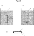
Fig. 2 ] A schematic drawing showing steps (I) through (K) of an embodiment of the method for manufacturing a graphene film of the present invention. - Hereinafter, one embodiment of the present invention will be described with reference to the drawings.
- In the present invention, first,
graphene 2 is prepared on asubstrate 1 as shown inFIG. 1A . A method of providing thegraphene 2 on thesubstrate 1 is not particularly limited, and a known method may be used. - As a preparation method of the
graphene 2, for example, mechanical peeling from graphite, a CVD method, a surface thermal decomposition method of a SiC substrate, and the like can be mentioned, but CVD method is preferable from the viewpoint of mass productivity. In this CVD method,graphene 2 is deposited on abase material 1 such as Ni foil, Cu foil or the like using a hydrocarbon gas as a raw material. Further, by attaching athermal release sheet 3 to the thus preparedgraphene 2, etching thebase material 1, attaching the thermal release sheet to anotherbase material 5, and then removing thethermal release sheet 3, the graphene can be transferred to the other substrate such as Si/SiO2. - There is no particular limitation on the
base material 1 used in this step, and a Ni foil, a Cu foil or a composite substrate made from the Ni foil or the Cu foil and a base material such as SiO2/Si or the like, or even the SiO2/Si after transferring graphene may be used as thebase material 1. In addition, although thisgraphene 2 is preferably made of a single layer from the viewpoint of transmittance, it may have a multilayer structure from the viewpoint of mechanical strength. Preferably, it is either of a single layer structure or a multilayer structure of about 2 to 100 layers. - Next, the
graphene 2 provided on thesubstrate 1 is covered up with theprotective film 3 as shown inFIG. 1 (B) . Now, theprotective film 3 is preferably resistant to a wet etching liquid to be used for removing thebase material 1 in a later step. In addition, the surface tension of the solvent which is to dissolve and remove thisprotective film 3 needs to be lower than the surface tension of the wet etching liquid. - The method of coating the
graphene 2 with theprotective film 3 may be appropriately selected based on the material used to make theprotective film 3. For example, when a resin is used to form theprotective film 3, thegraphene 2 can be coated with theprotective film 3 by applying the solution of the resin in a known manner such as spin coating or dip coating. and then removing the solvent from the solution. - In the present invention, as shown in
FIGS. 1 (D) and 1 (E) , thegraphene 2 provided on thebase material 1 is covered with theprotective film 3, and then thebase material 1 is removed by wet etching. In this wet etching, a liquid that can etch thesubstrate 1 is used as thewet etching liquid 6, and hence thewet etching liquid 6 may be appropriately selected based on the type of thesubstrate 1 to be etched. When thebase material 1 is made of SiO2/Si, for example, a 24% potassium hydroxide aqueous solution or the like can be used as thewet etching liquid 6. The surface tension of the 24% potassium hydroxide aqueous solution is 72 mN/m. - In this wet etching step, even though the
base material 1 is dissolved off, the film-like graphene 2 is yet supported by theprotective film 3, so that when thegraphene 2 is raised from thewet etching liquid 6, breakage of thegraphene 2 can be prevented thanks to theprotective film 3. It is also possible that theprotective film 3 prevents that surface of thegraphene 2 which is opposite to thebase material 1 from being damaged by thewet etching liquid 6. - Next, as shown in
FIGS. 2 (I) and 2 (J) , after thebase material 1 is removed by thewet etching liquid 6, a solvent 9 having a lower surface tension than thewet etching liquid 6 is used to dissolve and remove theprotective film 3. The solvent 9 is selected based on the type of theprotective film 3 and thewet etching liquid 6, and theprotective film 3 is also selected based on the type of the solvent 9 available. - For example, an acrylic resin can be selected as the
protective film 3 and acetone can be selected as the solvent 9. Or, a fluororesin can be selected as theprotective film 3 and a fluorine-based solvent can be selected as the solvent 9. In particular, since the fluororesin has high chemical resistance, it is preferable as theprotective film 3, and the fluorine-based solvent is preferable as the solvent 9 used in this step because its surface tension is generally low. - In this step, even though the
protective film 3 is dissolved and removed from thegraphene 2, the surface tension of the solvent 9 is so small that it is possible to lessen its stress on the film-like graphene 2, wherefore thegraphene 2 can be raised from the solvent 9 without breakage or other damages. - By using the film-shaped
graphene 2 thus obtained as the pellicle film which is attached to cover up the opening defined by the frame of the pellicle, it is possible to construct a pellicle. This pellicle may be provided with an adhesive for fixing the pellicle on the exposure original plate, a ventilation hole for adjusting the pressure inside the frame, a filter for preventing entry of foreign matter through the ventilation hole, etc.; the material and the shape of such added elements are not limited either. Furthermore, this pellicle is suitable as a pellicle for EUV exposure because it uses a graphene film with high transmittance for EUV light as the pellicle film. - Incidentally, in the method of manufacturing a graphene film of the present invention, it is possible to provide a holding
member 5 as shown inFIG. 1 (C) . Here, thegraphene 2 covered with theprotective film 3 and the holdingmember 5 are bonded together via an adhesive 4. This holdingmember 5 can be used for handling, for example, and it can be a metal frame or the like. As for the adhesive 4, it is not particularly limited, and any known adhesive may be used. - Although the timing of providing the holding
member 5 is not particularly limited, it is possible, for example, to provide it onto thegraphene 2 after thebase material 1 is removed by the wet etching, as shown inFIG. 1 (G) wherein the holding member is designated as 8, (such that thebase material 1 is replaced by the holding member 8). - In the present invention, a support member such as a support mesh film may be provided on the graphene film. With the support member provided, breakage of the graphene film in the manufacturing process can further be suppressed. In addition, it is also possible to increase the aperture ratio of the support mesh film, so that the transmittance of exposure light can be increased. As described above, the support member can be provided on the
graphene 2 after thebase material 1 is removed, as well as on theprotective film 3. - Further, the holding member may be caused to be the pellicle frame. By doing so, it is possible to obtain straightaway the graphene film and the pellicle frame joined together.
- First, a sample in which a 100-mm square graphene 2 (composed of 30 to 60 layers) was provided on a Si(SiO2/Si)
base material 1 having a SiO2 layer on its surface was prepared (FIG. 1 (A) ). Next, a fluororesin (Cytop CTX-S manufactured by Asahi Glass Co., Ltd.) as theprotective film 3 was applied to thegraphene 2 provided on thebase material 1 by spin coating in a manner such that its thickness becomes 1 µm after drying, and then it was cured by heating at 180°C for 1 minute (FIG. 1 (B) ). Subsequently, a 150-mm square SUS (stainless steel) frame serving as the holdingmember 5 was glued, via an epoxy resin-based adhesive 4 (EP330 manufactured by CEMEDINE CO., LTD.), on the fluororesin serving as theprotective film 3 in a manner such that theframe 5 surrounds thegraphene 2, when seen from above (Fig. 1 (C) ). - Next, this entity was immersed in a 24% potassium hydroxide aqueous solution (surface tension: 72 mN/m), whereby the SiO2/
Si base material 1 was caused to undergo wet etching. When the SiO2/Si substrate 1 was chemically removed, thegraphene 2 supported by the fluororesinprotective film 3 was taken out from the etching liquid, and thegraphene film 2 was found without breakage (FIG. 1(D), (E), (F) ). - Subsequently, a 100-mm square SUS frame serving also as the holding
member 8 was bonded to thegraphene film 2 supported by the fluororesinprotective film 3 via an epoxy resin-based adhesive 4 (EP330 manufactured by Cemedine Co., Ltd.) (Fig. 1(G) ). On this occasion, that part of the fluororesinprotective film 3 which lies outside of the 100-mmsquare SUS frame 8 was physically removed together with the holdingmember 5 and the adhesive 4 (FIG. 1 (H) ). - Next, this entity was vertically immersed in fluorine solvent 9 (NOVEC 7300, manufactured by Sumitomo 3M Ltd., surface tension: 15 mN/m) for 24 hours, whereby the fluororesin
protective film 3 was completely dissolved and removed; then the remnant entity was pulled up slowly and the thus obtainedgraphene film 2 was observed and found to have no damage or breakage (FIGS. 2 (I), (J), and (K) ). - First, a sample in which a 100-mm square graphene 2 (composed of 30 to 60 layers) was provided on a Si(SiO2/Si)
base material 1 having a SiO2 layer on its surface was prepared. Next, without applying anyprotective film 3 to thegraphene 2, the latter was directly bonded to a 100-mm square SUS frame using an epoxy resin-based adhesive 4 (EP330 manufactured by Cemedine Co., Ltd.). - Subsequently, this entity was immersed in a 24% potassium hydroxide aqueous solution (surface tension: 72 mN/m), whereby the SiO2/
Si base material 1 was caused to undergo wet etching. When the SiO2/Si base material 1 was removed, the appearance of thegraphene film 2 was observed and it was found that thegraphene film 2 had been eroded by theetching liquid 6 so much that there were even holes. Further, when thegraphene film 2 was taken out from thewet etching liquid 6, thegraphene film 2 was broken due to the relatively high surface tension of theetching liquid 6.
There is provided a method for preparing a graphene film for pellicle, and also a method for making a pellicle using such graphene film: wherein a film-like graphene deposited on a base material is coated with a protective film, from which the base material is chemically removed by an etching liquid and then the protective film is chemically removed by a solvent whose surface tension is lower than that of the etching liquid; the pellicle frame may be attached to the film-like graphene before the protective film is completely removed or thereafter. -
- 1:
- base material
- 2:
- graphene (graphene film)
- 3:
- protective film
- 4:
- adhesive
- 5, 8:
- holding member
- 6:
- wet etching liquid
- 7:
- adhesive
- 9:
- solvent
Claims (3)
- A method for manufacturing a graphene film characterised by including steps of:(i) preparing a film-like graphene provided on a base material; (ii) coating said graphene with a protective film; (iii) removing said base material by wet etching with an etching liquid; (iv) and dissolving the protective film using a solvent whose surface tension is lower than that of said wet etching liquid.
- The method for manufacturing a graphene film as claimed in Claim 1 wherein said protective film is a fluororesin, and said solvent is a fluorine-based solvent.
- A method for manufacturing a pellicle characterised by using a film-like graphene which is manufactured through steps including: (i) preparing a film-like graphene provided on a base material; (ii) coating said graphene with a protective film; (iii) removing said base material by wet etching with an etching liquid; (iv) dissolving the protective film using a solvent whose surface tension is lower than that of said wet etching liquid.
Applications Claiming Priority (1)
| Application Number | Priority Date | Filing Date | Title |
|---|---|---|---|
| JP2016220221A JP2018077412A (en) | 2016-11-11 | 2016-11-11 | Method for producing graphene film and method for producing pellicle using the same |
Publications (1)
| Publication Number | Publication Date |
|---|---|
| EP3321734A1 true EP3321734A1 (en) | 2018-05-16 |
Family
ID=60182451
Family Applications (1)
| Application Number | Title | Priority Date | Filing Date |
|---|---|---|---|
| EP17198221.8A Withdrawn EP3321734A1 (en) | 2016-11-11 | 2017-10-25 | Method of manufacturing graphene film and method of manufacturing pellicle using the same |
Country Status (6)
| Country | Link |
|---|---|
| US (1) | US10053367B2 (en) |
| EP (1) | EP3321734A1 (en) |
| JP (1) | JP2018077412A (en) |
| KR (1) | KR20180053251A (en) |
| CN (1) | CN108269735A (en) |
| TW (1) | TW201829310A (en) |
Cited By (2)
| Publication number | Priority date | Publication date | Assignee | Title |
|---|---|---|---|---|
| EP3418804A1 (en) * | 2017-06-23 | 2018-12-26 | Shin-Etsu Chemical Co., Ltd. | Pellicle film for photolithography and pellicle |
| EP3435155A1 (en) * | 2017-07-27 | 2019-01-30 | Samsung Electronics Co., Ltd. | Pellicle composition for photomask, pellicle for photomask formed from the pellicle composition, method of forming the pellicle, reticle including the pellicle, and exposure apparatus for lithography including the reticle |
Families Citing this family (10)
| Publication number | Priority date | Publication date | Assignee | Title |
|---|---|---|---|---|
| JP2020160345A (en) * | 2019-03-27 | 2020-10-01 | 三井化学株式会社 | Producing method of pellicle self-supporting film, producing method of pellicle, and producing method of semiconductor device |
| US20240018004A1 (en) * | 2020-11-18 | 2024-01-18 | Arcelormittal | Method for the manufacture of a self-standing graphene oxide or reduced graphene oxide film |
| KR102546968B1 (en) * | 2020-11-19 | 2023-06-23 | 주식회사 에프에스티 | Method for Fabricating Pellicle for EUV(extreme ultraviolet) Lithography |
| KR102668456B1 (en) * | 2020-12-07 | 2024-05-23 | 주식회사 에프에스티 | Pellicle Frame for EUV(extreme ultraviolet) Lithography |
| JP7810879B2 (en) * | 2021-12-23 | 2026-02-04 | 富士通株式会社 | How graphene is produced |
| KR20230128851A (en) | 2022-02-28 | 2023-09-05 | 삼성전자주식회사 | Method of manufacturing Pellicle structure |
| KR102442676B1 (en) * | 2022-04-15 | 2022-09-14 | 주식회사 그래핀랩 | Manufacturing method of graphene thin film for pellicle material using ozone gas |
| CN114990683A (en) * | 2022-06-06 | 2022-09-02 | 华北电力大学(保定) | Graphene coating stainless steel array microporous fiber and preparation method thereof |
| CN119790350A (en) | 2022-09-15 | 2025-04-08 | 日本碍子株式会社 | EUV transmissive membrane |
| KR102949961B1 (en) * | 2022-10-07 | 2026-04-08 | 주식회사 참그래핀 | The manufacturing method of graphene membrane pellicle for extreme ultra violet lithography |
Citations (6)
| Publication number | Priority date | Publication date | Assignee | Title |
|---|---|---|---|---|
| WO2013096841A1 (en) * | 2011-12-22 | 2013-06-27 | The Trustees Of Columbia University In The City Of New York | Assisted transfer of graphene |
| JP2013534727A (en) | 2010-06-25 | 2013-09-05 | エーエスエムエル ネザーランズ ビー.ブイ. | Lithographic apparatus and lithography method |
| JP2015018228A (en) | 2013-06-10 | 2015-01-29 | 旭化成イーマテリアルズ株式会社 | Pellicle membrane and pellicle |
| US20150309404A1 (en) * | 2014-04-24 | 2015-10-29 | Taiwan Semiconductor Manufacturing Co., Ltd | Pellicle structure and method for forming the same |
| US20160139500A1 (en) * | 2014-11-13 | 2016-05-19 | Samsung Electronics Co., Ltd. | Methods of manufacturing pellicles having graphite layers |
| US20160201201A1 (en) * | 2015-01-09 | 2016-07-14 | SungKyunKwan University's Research & Business Foundation | Pellicles and methods of manufacturing the same |
Family Cites Families (1)
| Publication number | Priority date | Publication date | Assignee | Title |
|---|---|---|---|---|
| JP6326056B2 (en) * | 2013-09-30 | 2018-05-16 | 三井化学株式会社 | Pellicle film, pellicle using the same, exposure original plate and exposure apparatus, and method for manufacturing semiconductor device |
-
2016
- 2016-11-11 JP JP2016220221A patent/JP2018077412A/en active Pending
-
2017
- 2017-10-25 EP EP17198221.8A patent/EP3321734A1/en not_active Withdrawn
- 2017-11-09 US US15/808,143 patent/US10053367B2/en active Active
- 2017-11-09 KR KR1020170148824A patent/KR20180053251A/en not_active Withdrawn
- 2017-11-10 CN CN201711106323.9A patent/CN108269735A/en active Pending
- 2017-11-10 TW TW106138851A patent/TW201829310A/en unknown
Patent Citations (6)
| Publication number | Priority date | Publication date | Assignee | Title |
|---|---|---|---|---|
| JP2013534727A (en) | 2010-06-25 | 2013-09-05 | エーエスエムエル ネザーランズ ビー.ブイ. | Lithographic apparatus and lithography method |
| WO2013096841A1 (en) * | 2011-12-22 | 2013-06-27 | The Trustees Of Columbia University In The City Of New York | Assisted transfer of graphene |
| JP2015018228A (en) | 2013-06-10 | 2015-01-29 | 旭化成イーマテリアルズ株式会社 | Pellicle membrane and pellicle |
| US20150309404A1 (en) * | 2014-04-24 | 2015-10-29 | Taiwan Semiconductor Manufacturing Co., Ltd | Pellicle structure and method for forming the same |
| US20160139500A1 (en) * | 2014-11-13 | 2016-05-19 | Samsung Electronics Co., Ltd. | Methods of manufacturing pellicles having graphite layers |
| US20160201201A1 (en) * | 2015-01-09 | 2016-07-14 | SungKyunKwan University's Research & Business Foundation | Pellicles and methods of manufacturing the same |
Non-Patent Citations (1)
| Title |
|---|
| KWON KI CHANG ET AL: "Fluoropolymer-assisted graphene electrode for organic light-emitting diodes", ORGANIC ELECTRONICS, vol. 15, no. 11, 30 November 2014 (2014-11-30), pages 3154 - 3161, XP029076514, ISSN: 1566-1199, DOI: 10.1016/J.ORGEL.2014.08.041 * |
Cited By (4)
| Publication number | Priority date | Publication date | Assignee | Title |
|---|---|---|---|---|
| EP3418804A1 (en) * | 2017-06-23 | 2018-12-26 | Shin-Etsu Chemical Co., Ltd. | Pellicle film for photolithography and pellicle |
| US10761421B2 (en) | 2017-06-23 | 2020-09-01 | Shin-Etsu Chemical Co., Ltd. | Pellicle film for photolithography and pellicle |
| EP3435155A1 (en) * | 2017-07-27 | 2019-01-30 | Samsung Electronics Co., Ltd. | Pellicle composition for photomask, pellicle for photomask formed from the pellicle composition, method of forming the pellicle, reticle including the pellicle, and exposure apparatus for lithography including the reticle |
| US10551735B2 (en) | 2017-07-27 | 2020-02-04 | Samsung Electronics Co., Ltd. | Pellicle composition for photomask, pellicle for photomask formed from the pellicle composition, method of forming the pellicle, reticle including the pellicle, and exposure apparatus for lithography including the reticle |
Also Published As
| Publication number | Publication date |
|---|---|
| JP2018077412A (en) | 2018-05-17 |
| CN108269735A (en) | 2018-07-10 |
| TW201829310A (en) | 2018-08-16 |
| US10053367B2 (en) | 2018-08-21 |
| US20180134561A1 (en) | 2018-05-17 |
| KR20180053251A (en) | 2018-05-21 |
Similar Documents
| Publication | Publication Date | Title |
|---|---|---|
| US10053367B2 (en) | Method of manufacturing graphene film and method of manufacturing pellicle using the same | |
| TWI830485B (en) | Pellicle frame, pellicle, photomask with pellicle, exposure method, method of manufacturing a pattern, and method of manufacturing a semiconductor device | |
| JP5189614B2 (en) | Pellicle, method of attaching the pellicle, mask with pellicle and mask | |
| JP5478463B2 (en) | Pellicle for lithography | |
| JP7224712B2 (en) | A method for manufacturing a pellicle, a pellicle, a photomask with a pellicle, an exposure method, a method for manufacturing a semiconductor device, a method for manufacturing a liquid crystal display, and a method for manufacturing an organic EL display. | |
| EP3671343A1 (en) | Pellicle film for photolithography and pellicle provided with the same | |
| TWI815825B (en) | Protective film frame and protective film components | |
| KR20130074066A (en) | Euv pellicle and manufacturing method of the same | |
| TWI707196B (en) | Dustproof film assembly for EUV exposure, exposure master with dustproof film assembly, and manufacturing method of semiconductor device or liquid crystal display panel | |
| WO2011125407A1 (en) | Photomask unit and method of manufacturing same | |
| KR102947939B1 (en) | Pellicle, exposure plate, exposure device, method for manufacturing a pellicle, and method for manufacturing a semiconductor device | |
| US20110129767A1 (en) | Pellicle for lithography | |
| KR20240121338A (en) | Pellicle, original plate for light exposure, light exposure device, method for producing pellicle, and method for producing semiconductor device | |
| CN103901716B (en) | Dust-proof pellicle for lithography | |
| CN217821249U (en) | Pellicle frame, pellicle, photomask including the pellicle frame, and system including the photomask | |
| TWI924786B (en) | Pellicle, exposure original plate, exposure device, method of manufacturing pellicle film, and method of manufacturing semiconductor device |
Legal Events
| Date | Code | Title | Description |
|---|---|---|---|
| PUAI | Public reference made under article 153(3) epc to a published international application that has entered the european phase |
Free format text: ORIGINAL CODE: 0009012 |
|
| AK | Designated contracting states |
Kind code of ref document: A1 Designated state(s): AL AT BE BG CH CY CZ DE DK EE ES FI FR GB GR HR HU IE IS IT LI LT LU LV MC MK MT NL NO PL PT RO RS SE SI SK SM TR |
|
| AX | Request for extension of the european patent |
Extension state: BA ME |
|
| STAA | Information on the status of an ep patent application or granted ep patent |
Free format text: STATUS: THE APPLICATION IS DEEMED TO BE WITHDRAWN |
|
| 18D | Application deemed to be withdrawn |
Effective date: 20181117 |