EP3320570B1 - Wavelength converted light emitting device - Google Patents
Wavelength converted light emitting device Download PDFInfo
- Publication number
- EP3320570B1 EP3320570B1 EP16732645.3A EP16732645A EP3320570B1 EP 3320570 B1 EP3320570 B1 EP 3320570B1 EP 16732645 A EP16732645 A EP 16732645A EP 3320570 B1 EP3320570 B1 EP 3320570B1
- Authority
- EP
- European Patent Office
- Prior art keywords
- phosphor
- dopant concentration
- light
- light source
- region
- Prior art date
- Legal status (The legal status is an assumption and is not a legal conclusion. Google has not performed a legal analysis and makes no representation as to the accuracy of the status listed.)
- Active
Links
Images
Classifications
-
- H—ELECTRICITY
- H10—SEMICONDUCTOR DEVICES; ELECTRIC SOLID-STATE DEVICES NOT OTHERWISE PROVIDED FOR
- H10H—INORGANIC LIGHT-EMITTING SEMICONDUCTOR DEVICES HAVING POTENTIAL BARRIERS
- H10H20/00—Individual inorganic light-emitting semiconductor devices having potential barriers, e.g. light-emitting diodes [LED]
- H10H20/80—Constructional details
- H10H20/85—Packages
- H10H20/851—Wavelength conversion means
- H10H20/8516—Wavelength conversion means having a non-uniform spatial arrangement or non-uniform concentration, e.g. patterned wavelength conversion layer or wavelength conversion layer with a concentration gradient
-
- H—ELECTRICITY
- H10—SEMICONDUCTOR DEVICES; ELECTRIC SOLID-STATE DEVICES NOT OTHERWISE PROVIDED FOR
- H10H—INORGANIC LIGHT-EMITTING SEMICONDUCTOR DEVICES HAVING POTENTIAL BARRIERS
- H10H20/00—Individual inorganic light-emitting semiconductor devices having potential barriers, e.g. light-emitting diodes [LED]
- H10H20/80—Constructional details
- H10H20/85—Packages
- H10H20/851—Wavelength conversion means
- H10H20/8511—Wavelength conversion means characterised by their material, e.g. binder
- H10H20/8512—Wavelength conversion materials
-
- H—ELECTRICITY
- H10—SEMICONDUCTOR DEVICES; ELECTRIC SOLID-STATE DEVICES NOT OTHERWISE PROVIDED FOR
- H10H—INORGANIC LIGHT-EMITTING SEMICONDUCTOR DEVICES HAVING POTENTIAL BARRIERS
- H10H20/00—Individual inorganic light-emitting semiconductor devices having potential barriers, e.g. light-emitting diodes [LED]
- H10H20/80—Constructional details
- H10H20/85—Packages
- H10H20/851—Wavelength conversion means
- H10H20/8511—Wavelength conversion means characterised by their material, e.g. binder
- H10H20/8512—Wavelength conversion materials
- H10H20/8513—Wavelength conversion materials having two or more wavelength conversion materials
-
- H—ELECTRICITY
- H10—SEMICONDUCTOR DEVICES; ELECTRIC SOLID-STATE DEVICES NOT OTHERWISE PROVIDED FOR
- H10H—INORGANIC LIGHT-EMITTING SEMICONDUCTOR DEVICES HAVING POTENTIAL BARRIERS
- H10H20/00—Individual inorganic light-emitting semiconductor devices having potential barriers, e.g. light-emitting diodes [LED]
- H10H20/80—Constructional details
- H10H20/85—Packages
- H10H20/851—Wavelength conversion means
- H10H20/8511—Wavelength conversion means characterised by their material, e.g. binder
Definitions
- the present invention relates to wavelength converted light emitting devices such as light emitting diodes.
- LEDs light emitting diodes
- RCLEDs resonant cavity light emitting diodes
- VCSELs vertical cavity laser diodes
- edge emitting lasers are among the most efficient light sources currently available.
- Materials systems currently of interest in the manufacture of high-brightness light emitting devices capable of operation across the visible spectrum include Group III-V semiconductors, particularly binary, ternary, and quaternary alloys of gallium, aluminum, indium, and nitrogen, also referred to as III-nitride materials.
- III-nitride light emitting devices are fabricated by epitaxially growing a stack of semiconductor layers of different compositions and dopant concentrations on a sapphire, silicon carbide, III-nitride, or other suitable substrate by metal-organic chemical vapor deposition (MOCVD), molecular beam epitaxy (MBE), or other epitaxial techniques.
- MOCVD metal-organic chemical vapor deposition
- MBE molecular beam epitaxy
- the stack often includes one or more n-type layers doped with, for example, Si, formed over the substrate, one or more light emitting layers in an active region formed over the n-type layer or layers, and one or more p-type layers doped with, for example, Mg, formed over the active region. Electrical contacts are formed on the n- and p-type regions.
- the blue light from an LED or laser illuminates a yellow-green phosphor, such as a YAG:Ce phosphor, or a combination of red and green phosphors, so that the combination of the light generated by the phosphor and the blue light leaking through creates white light.
- a yellow-green phosphor such as a YAG:Ce phosphor, or a combination of red and green phosphors
- Some phosphors are quenched or saturated under very bright blue light (e.g., above 100 W/cm 2 ) produced by a high power blue light source. Quenching or saturation may lead to undesirable color shifts and reduced light output.
- a phosphor is essentially a crystalline host material (sometimes called a lattice) doped with activators or dopants ("activators” and “dopants” are used interchangeably herein). Examples of common activator species include Eu 2+ , Eu 3+ , and Ce 3+ . When the phosphor is exposed to light in a particular wavelength range (the excitation spectrum), the activators absorb the excitation light and emit light of a longer wavelength (the emission spectrum).
- some phosphors become saturated when exposed to, for example, blue light from an LED.
- the efficiency of the phosphor decreases.
- the reduction in efficiency with increasing excitation density may be referred to herein as "droop.”
- Excited state interaction may include exited state absorption (ESA) and quantum-mechanical interaction (QMI).
- ESA may depend on the electronic band structure of the host, and/or the energetic position of dopant levels relative to the host band structure.
- QMI may depend on the crystal structure of the host; in particular, the distance between the emitting and the absorbing exited dopants.
- a photon emitted by an excited activator may absorbed by another already excited activator, exciting an electron into the host material conduction band rather than emitting a photon, thereby reducing the efficiency of the phosphor. This effect may be more prevalent at higher temperatures.
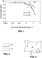
- Fig. 1 is a plot of measured quantum efficiency as a function of irradiance from a blue-emitting laser (in W/mm 2 ).
- the two phosphors illustrated in Fig. 1 have the same host material, (Ba 0.1 Sr 0.9 ) 2 Si 5 N 8 , and the same activator, Eu 2+ .
- Two different activator concentrations are illustrated, 0.5% (curve 10) and 2.4% (curve 14).
- the efficiency of the phosphor at the highest excitation densities is lower than the efficiency of the phosphor with the lowest activator concentration at the highest excitation densities.
- phosphors are synthesized or applied to a device in such a way as to reduce or eliminate droop, the observed efficiency drop at increasing excitation density.
- the host material of the phosphors in the embodiments described below may be, for example, CaS, (Ca,Sr)Ga 2 S 4 , Ba 2-x M x Si 5-y Al y N 8-y O y , wherein M represents Sr or Ca, 0 ⁇ x ⁇ 1, and 0.0005 ⁇ y ⁇ 0.05 (BSSNE), Ca 1-x Sr x AlSiN3, wherein 0 ⁇ x ⁇ 1, preferably 0 ⁇ x ⁇ 0.95 (SCASN), eCas, YAG, or any other suitable host material.
- the activator in the phosphors in the embodiments described herein may be, for example, a rare earth material, Europium, Eu 2+ , Cerium, Ce 3+ , or any other suitable material.
- the activator is Europium.
- Cerium-doped phosphors may also experience droop, often at much higher incident power densities than Europium-doped phosphors.
- a Ce 3+ phosphor may exhibit similar droop at about 50 W/mm 2 that an Eu 2+ phosphor exhibits at 1 W/mm 2 .
- Fig. 2 illustrates a device according to embodiments of the invention.
- a wavelength converting structure 20 is disposed in a path of light emitted from a light emitting device 18 such as a light emitting diode (LED).
- the wavelength converting structure 20 is a phosphor, which includes a host and a dopant.
- Wavelength converting structure 20 may be in direct contact with light emitting device 18 or it may be spaced apart from the light emitting device 18.
- Wavelength converting structure 20 includes one or more phosphors.
- one or more optical elements such as lenses (not shown in Fig. 2 ) may be included in the device of Fig. 2 .
- an optical element may be disposed between light emitting device 18 and wavelength converting structure 20, in order to shape, filter, and/or at least partially collimate light extracted from the light emitting device 18.
- an optical element may be disposed over wavelength converting structure 20, in order to shape, filter, and/or at least partially collimate light extracted from the wavelength converting structure 20.
- optical elements include filters, dome lenses, Fresnel lenses, compound parabolic concentrators, and any other suitable structure.
- a maximum average dopant concentration in the wavelength converting structure 20 is selected for a predetermined amount of light produced by the light emitting device 18 and converted by wavelength converting structure 20, and for a predetermined maximum reduction in efficiency of the wavelength converting structure at increasing excitation density (i.e. maximum allowed droop).
- the predetermined maximum reduction in efficiency may result in a color shift of the resulting total emission.
- the wavelength converting structure 20 may be a phosphor layer of substantially uniform average dopant concentration, a layered structure, or a graded composition structure, such as the phosphors described in any of the examples below.
- the thickness of the wavelength converting structure 20 of Fig. 2 is limited.
- droop may be reduced by lowering the dopant concentration, but as the dopant concentration is reduced, a predetermined amount of converted light demands greater thickness, to a limit where a dopant concentration approaching zero requires an infinite thickness.
- a maximum average dopant concentration in the wavelength converting structure 20 is selected for a predetermined wavelength converting structure thickness 20, and for a predetermined maximum reduction in efficiency of the wavelength converting structure at increasing excitation density (i.e. maximum allowed droop).
- the light emitting device 18 may be any suitable device that emits light that may excite one or more wavelength converting materials in wavelength converting structure 20.
- light emitting device 18 is a III-nitride LED that emits blue or UV light.
- a III-nitride LED may be, for example, a flip chip device, where a majority of light is extracted through a surface of the LED opposite a surface on which electrical contacts are formed; a vertical device, where electrical contacts are formed on opposite sides of the device; or a lateral device, where both electrical contacts are formed on a surface of the device through which a majority of light is extracted.
- the growth substrate on which the III-nitride device layers are grown may be part of the device, may be thinned, or may be completely removed. Any suitable light emitting device may be used.
- semiconductor light emitting devices are III-nitride LEDs that emit blue or UV light
- semiconductor light emitting devices besides LEDs such as laser diodes and semiconductor light emitting devices made from other materials systems such as other III-V materials, III-phosphide, III-arsenide, II-VI materials, ZnO, or Si-based materials may be used, as long as the emission of the device overlaps with the excitation spectrum of the wavelength converting structure 20.
- Suitable wavelength converting structures 20 may include one or more of the phosphors and/or structures described in the embodiments below.
- the wavelength converting structure 20 may be disposed on the LED, or spaced apart from the LED.
- the concentration of dopant in the wavelength converting structure, and/or the arrangement of the dopant are selected such that a predetermined light emission from the light emitting structure 18, a predetermined maximum reduction of the efficiency of the wavelength converting structure is not surpassed (i.e., a maximum droop level is not exceeded).
- the wavelength converting structure includes one or more wavelength converting materials which may be, for example, conventional phosphors, organic phosphors, quantum dots, organic semiconductors, II-VI or III-V semiconductors, II-VI or III-V semiconductor quantum dots or nanocrystals, dyes, polymers, or other materials that luminesce.
- the wavelength converting material absorbs light emitted by the LED and emits light of one or more different wavelengths. Unconverted light emitted by the LED is often part of the final spectrum of light extracted from the structure, though it need not be.
- the final spectrum of light extracted from the structure may be white, polychromatic, or monochromatic.
- Examples of common combinations include a blue-emitting LED combined with a yellow-emitting wavelength converting material, a blue-emitting LED combined with green- and red-emitting wavelength converting materials, a UV-emitting LED combined with blue- and yellow-emitting wavelength converting materials, and a UV-emitting LED combined with blue-, green-, and red-emitting wavelength converting materials.
- Wavelength converting materials emitting other colors of light may be added to tailor the spectrum of light extracted from the structure.
- the wavelength converting structure may include light scattering or light diffusing elements e.g. TiO 2 .
- wavelength converting structure 20 is a structure that is fabricated separately from the LED and attached to the LED, for example through wafer bonding or a suitable adhesive such as silicone or epoxy.
- a prefabricated wavelength converting element is a ceramic phosphor, which is formed by, for example, sintering powder phosphor or the precursor materials of phosphor into a ceramic slab, which may then be diced into individual wavelength converting elements.
- a ceramic phosphor may also be formed by, for example tape casting, where the ceramic is fabricated to the correct shape, with no dicing or cutting necessary.
- suitable non-ceramic preformed wavelength converting elements include powder phosphors that are dispersed in transparent material such as silicone or glass that is rolled, cast, or otherwise formed into a sheet, then singulated into individual wavelength converting elements, and phosphor mixed with silicone and disposed on a transparent substrate.
- a reflecting material (not shown in Fig. 2 ) may be disposed on the sides of the LEDs and the wavelength converting element, in order to force light to exit the device through the top surface.
- wavelength converting structure 20 includes a phosphor including a host material and an activator that at certain activator concentrations does suffer from droop.
- the phosphor is doped to an activator concentration that does not exhibit a decrease in efficiency at increasing excitation intensity.
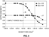
- the efficiency curve of such a phosphor is illustrated in Fig. 3 (the phosphor illustrated in Fig. 3 may be the same phosphor illustrated in Fig. 1 ).
- Fig. 3 is a plot, for two phosphors with the same host and different dopant concentrations, of emitted power/incident power for a given phosphor thickness, as a function of incident power (excitation density).
- Curve 22 represents a phosphor with a higher activator concentration than the phosphor of curve 24.
- the phosphor with the higher activator concentration exhibits droop (curve 22) at the incident power indicated at 25, while the phosphor with the lower activator concentration (curve 24) does not exhibit droop at the incident power indicated at 25.
- the phosphor includes a host material that at certain activator concentrations does suffer from droop at a selected excitation density (i.e., curve 22 at incident power 25). The activator concentration may be reduced such that the phosphor does not suffer from droop at a given excitation density (i.e., curve 24 at incident power 25). At excitation densities other than the selected excitation density, the phosphor may exhibit droop (i.e., curve 24 at incident power 27).
- the activator in the phosphors represented by curves 22 and 24 may be, for example, a rare earth material, Europium, or Eu 2+ in some embodiments.
- the phosphor illustrated by curve 24 may emit less light at a given incident power density than the phosphor illustrated by curve 22. Accordingly, to reach a given brightness, more phosphor may be used in a device where the wavelength converting structure 20 includes phosphor represented by curve 24.
- the phosphor illustrated by curve 24 is included in wavelength converting structure 20.
- the phosphor illustrated by curve 22 is not included in the device, rather it is described above as a reference against which the performance of the phosphors illustrated by curve 24 is compared.
- the phosphor illustrated by curve 24 may be, in some embodiments, the only phosphor with that host material included in wavelength converting structure 20.
- the phosphor illustrated by curve 24 may be disposed in a single layer of substantially uniform dopant concentration.
- the activator concentration in the phosphor illustrated by curve 24 is substantially uniform throughout wavelength converting structure 20, i.e. the activator concentration is not graded in a horizontal or vertical plane in wavelength converting structure 20.
- wavelength converting structure 20 includes a powder phosphor that is produced to increase the distance between activators within each phosphor particle, which may reduce or eliminate droop.
- a phosphor portion 30 may be characterized by a spacing 34 between activators 32, as illustrated in Fig. 4 .
- the spacing 34 may be increased, as compared to a given commercially used phosphor with the same host material and the same activator concentration.
- the activator 32 is a rare earth material, Europium, or Eu 2+ .
- the average spacing 34 may be at least 15 ⁇ in some embodiments, at least 18 ⁇ in some embodiments, at least 20 ⁇ in some embodiments, at least 25 ⁇ in some embodiments, and no more than 50 ⁇ in some embodiments.
- the wavelength converting structure 20 includes a phosphor with a graded concentration of activators.
- the activator concentration may be graded in a direction perpendicular to a major surface of the wavelength converting structure 20.
- the activator concentration is lowest in a region closest to the excitation light source, and highest in a region furthest from the excitation light source.
- the excitation power decreases exponentially with depth into the phosphor.
- the excitation density is reduced.
- the droop exhibited by the phosphor may also decrease.
- droop may be reduced or eliminated, as compared to the same phosphor when homogeneously doped.
- graded the activator concentration may refer to any change in concentration other than a single, stepwise change in concentration.
- the graded activator concentration profile may take any shape including, for example, a linear, step-graded, or a power law profile, and may include multiple or no regions of constant activator concentration.
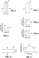
- Fig. 5 illustrates one example of a slab-type graded wavelength converting structure 20.
- the wavelength converting structure 20 includes multiple layers 52, 54, 56, and 58 of different activator concentration. Within each of layers 52, 54, 56, and 58, the activator concentration may be constant and uniform, though this is not required.
- the wavelength converting structure 20 of Fig. 5 may be a ceramic, or any other suitable structure. Though four layers are illustrated in Fig. 5 , more or fewer layers may be used. In some embodiments, two to ten layers are included.
- the total thickness of the wavelength converting structure 20 of Fig. 5 may be at least 100 ⁇ m thick in some embodiments, no more than 400 ⁇ m thick in some embodiments, at least 200 ⁇ m thick in some embodiments, and no more than 300 ⁇ m thick in some embodiments.
- Each layer may be the same thickness, though this is not required.
- Each layer may have a thickness of at least 10 ⁇ m in some embodiments and no more than 100 ⁇ m in some embodiments.
- the surface 50 of wavelength converting structure 20 faces the light source 18. Accordingly, layer 52 has the lowest activator concentration.
- the surface 60 of wavelength converting structure 20 is furthest from the light source. Accordingly, layer 58 has the highest activator concentration.
- Fig. 6 illustrates the activator concentration as a function of position from surface 50 to surface 60 for one example of a wavelength converting structure 20. Four layers of constant and different activator concentration are illustrated. The concentration increases from surface 50 to surface 60 in multiple steps.
- Fig. 7 illustrates another example of a slab-type wavelength converting structure 20.
- the wavelength converting structure of Fig. 7 is continuously graded, rather than stepwise graded, as illustrated in Fig. 5 .
- surface 50 is closest to the light source and surface 60 is furthest from the light source.
- Figs. 8 and 9 illustrate two possible grading profiles for the structure of Fig. 7 , in plots of activator concentration as a function of position. In each grading profile, the activator concentration increases from a lowest concentration at surface 50 to a highest concentration at surface 60.
- Fig. 8 illustrates a linear grading profile.
- Fig. 9 illustrates a quadratic grading profile. Other profiles such as exponential, polynomial, or any other suitable profile can be used to grade the wavelength converting structure 20.
- the individual particles in a powder phosphor have a dopant concentration that varies across the particle.
- An individual particle has a first region with a first average dopant concentration and a second region with a second average dopant concentration, where the first and second average dopant concentrations are different. The first and second regions are arranged to reduce or eliminate droop.
- the same effect described in the graded phosphors of Figs. 5 and 7 , where a more highly doped portion of the phosphor is "screened" by a lower doped portion of the phosphor, reducing the excitation density in the more highly doped portion, may be achieved in a powder phosphor by forming the phosphor particles with a dopant concentration that varies across the particle, such that the center portion of each particle is more highly doped than the outer portion of each particle.
- Fig. 11 is a plot of dopant concentration as a function of diameter for one example of such a phosphor particle.
- 70 and 72 represent the outer edges of the particle
- 74 represents the center.
- the dopant concentration is lower at the edges of the particle than at the center, where it is highest.
- the lower doped outer portion of each particle is the first part of the particle that "sees" light from the light emitting diode.
- the lower doped outer portion of each particle therefore reduces the excitation density at the more highly doped center, which may reduce the droop and may increase the efficiency of the phosphor.
- the concentration gradient in the phosphor particle is not limited to the particular profile illustrated in Fig. 11 .
- Phosphor particles with the center more highly doped than the outer portion may be formed by providing or synthesizing a doped core, growing a non-doped shell around the doped core, and diffusing the dopant in a thermal process partially into the outer region.
- the activator may be, for example, a rare earth material, Cerium, Ce 3+ , Europium, or Eu 2+ .
- Fig. 10 illustrates a wavelength converting structure 20 with a structure that screens a phosphor that exhibits droop, in order to reduce the excitation density of that phosphor.
- the screening structure 66 is disposed closest to the light source.
- a phosphor 68 which exhibits a drop in efficiency at increasing excitation density is disposed furthest from the light source.
- the screening structure 66 absorbs light from the light source, effectively reducing the excitation density incident on phosphor 68.
- the characteristics of the screening structure 66 such as the material, thickness, and absorption coefficient, may be selected to reduce the excitation density incident on the phosphor 68 to a point where a predetermined maximum reduction of the phosphor's efficiency is not surpassed.
- suitable screening structures 66 include non-wavelength converting materials, wavelength converting materials, phosphors, layers designed to scatter light, filters, reflectors, and any other suitable structure.
- structure 66 is a second phosphor, which does not exhibit a drop in efficiency at increasing excitation density, or which exhibits less droop than phosphor 68.
- structure 66 is a garnet phosphor, a YAG:Ce phosphor, or any other suitable phosphor.
Landscapes
- Luminescent Compositions (AREA)
- Led Device Packages (AREA)
Description
- The present invention relates to wavelength converted light emitting devices such as light emitting diodes.
- Semiconductor light-emitting devices including light emitting diodes (LEDs), resonant cavity light emitting diodes (RCLEDs), vertical cavity laser diodes (VCSELs), and edge emitting lasers are among the most efficient light sources currently available. Materials systems currently of interest in the manufacture of high-brightness light emitting devices capable of operation across the visible spectrum include Group III-V semiconductors, particularly binary, ternary, and quaternary alloys of gallium, aluminum, indium, and nitrogen, also referred to as III-nitride materials. Typically, III-nitride light emitting devices are fabricated by epitaxially growing a stack of semiconductor layers of different compositions and dopant concentrations on a sapphire, silicon carbide, III-nitride, or other suitable substrate by metal-organic chemical vapor deposition (MOCVD), molecular beam epitaxy (MBE), or other epitaxial techniques. The stack often includes one or more n-type layers doped with, for example, Si, formed over the substrate, one or more light emitting layers in an active region formed over the n-type layer or layers, and one or more p-type layers doped with, for example, Mg, formed over the active region. Electrical contacts are formed on the n- and p-type regions.
- To create a white light solid state light source, the blue light from an LED or laser illuminates a yellow-green phosphor, such as a YAG:Ce phosphor, or a combination of red and green phosphors, so that the combination of the light generated by the phosphor and the blue light leaking through creates white light. Some phosphors are quenched or saturated under very bright blue light (e.g., above 100 W/cm2) produced by a high power blue light source. Quenching or saturation may lead to undesirable color shifts and reduced light output. In
US 2012/0141771 A1 andUS 2015/0008463 A1 , structures including a blue Light Emitting Diode (LED) and phosphors disposed in a path of light emitted by the light source are disclosed. The phosphors have different dopant concentrations in different regions. - It is an object of the invention to provide a wavelength converted light emitting device with a wavelength converting material that is efficient even at high excitation density.
- It is an object of the invention to avoid or minimize color shifts with increasing brightness in phosphor converted light sources, in particular where two or more phosphors are used to generate, for example, warm white light, which may require constant conversion efficiencies for all phosphors used.
- Structures according to embodiments of the invention are defined in
independent claims 1 and 7. Preferred embodiments are defined in the dependent claims. -
- Fig. 1
- is a plot of quantum efficiency as a function of irradiance, for two phosphors with the same host, (Ba0.1Sr0.9)2Si5N8, and different concentrations of the dopant Eu2+.
- Fig. 2
- is a cross section of a device including a light source and a wavelength converting structure.
- Fig. 3
- is a plot of power emitted/incident power as a function of excitation density for two materials, one that exhibits droop (i.e. a reduction in efficiency of the phosphor at increasing excitation density) at a given excitation density, and one that does not exhibit droop at the given excitation density, such as, for example, 0.2 W/mm2.
- Fig. 4
- illustrates a portion of a surface of a phosphor particle.
- Fig. 5
- is a cross section of a step graded wavelength converting structure.
- Fig. 6
- is a plot of activator concentration as a function of position for one example of the structure of
Fig. 8 . - Fig. 7
- is a cross section of a continuously graded wavelength converting structure.
- Figs. 8 and 9
- are plots of activator concentration as a function of position for two examples of the structure of
Fig. 7 . - Fig. 10
- is a cross section of a wavelength converting structure including multiple phosphors.
- Fig. 11
- is a plot of concentration as a function of position for a phosphor particle.
- A phosphor is essentially a crystalline host material (sometimes called a lattice) doped with activators or dopants ("activators" and "dopants" are used interchangeably herein). Examples of common activator species include Eu2+, Eu3+, and Ce3+. When the phosphor is exposed to light in a particular wavelength range (the excitation spectrum), the activators absorb the excitation light and emit light of a longer wavelength (the emission spectrum).
- As described above, some phosphors become saturated when exposed to, for example, blue light from an LED. In particular, as the excitation density increases (i.e., the amount of light per area incident on the phosphor), the efficiency of the phosphor decreases. The reduction in efficiency with increasing excitation density may be referred to herein as "droop."
- Many processes may cause or exacerbate droop. Without limiting embodiments of the invention to any particular theory, two processes that may influence droop are ground state exhaustion and excited state interaction. (Embodiments of the invention may not address ground state exhaustion.) Excited state interaction may include exited state absorption (ESA) and quantum-mechanical interaction (QMI). ESA may depend on the electronic band structure of the host, and/or the energetic position of dopant levels relative to the host band structure. QMI may depend on the crystal structure of the host; in particular, the distance between the emitting and the absorbing exited dopants. For example, a photon emitted by an excited activator may absorbed by another already excited activator, exciting an electron into the host material conduction band rather than emitting a photon, thereby reducing the efficiency of the phosphor. This effect may be more prevalent at higher temperatures.
- As the activator concentration increases, the decrease in efficiency at any excitation density may become more pronounced, as illustrated in
Fig. 1. Fig. 1 is a plot of measured quantum efficiency as a function of irradiance from a blue-emitting laser (in W/mm2). The two phosphors illustrated inFig. 1 have the same host material, (Ba0.1Sr0.9)2Si5N8, and the same activator, Eu2+. Two different activator concentrations are illustrated, 0.5% (curve 10) and 2.4% (curve 14). As illustrated inFig. 1 , for the higher activator concentrations, the efficiency of the phosphor at the highest excitation densities is lower than the efficiency of the phosphor with the lowest activator concentration at the highest excitation densities. - In embodiments of the invention, phosphors are synthesized or applied to a device in such a way as to reduce or eliminate droop, the observed efficiency drop at increasing excitation density. The host material of the phosphors in the embodiments described below may be, for example, CaS, (Ca,Sr)Ga2S4, Ba2-xMxSi5-yAlyN8-yOy, wherein M represents Sr or Ca, 0 ≤ x ≤ 1, and 0.0005 < y < 0.05 (BSSNE), Ca1-xSrxAlSiN3, wherein 0 ≤ x ≤ 1, preferably 0 < x < 0.95 (SCASN), eCas, YAG, or any other suitable host material. The activator in the phosphors in the embodiments described herein may be, for example, a rare earth material, Europium, Eu2+, Cerium, Ce3+, or any other suitable material. In the examples below, the activator is Europium. However, Cerium-doped phosphors may also experience droop, often at much higher incident power densities than Europium-doped phosphors. For example, a Ce3+ phosphor may exhibit similar droop at about 50 W/mm2 that an Eu2+ phosphor exhibits at 1 W/mm2.
-
Fig. 2 illustrates a device according to embodiments of the invention. Awavelength converting structure 20 is disposed in a path of light emitted from alight emitting device 18 such as a light emitting diode (LED). Thewavelength converting structure 20 is a phosphor, which includes a host and a dopant.Wavelength converting structure 20 may be in direct contact with light emittingdevice 18 or it may be spaced apart from thelight emitting device 18.Wavelength converting structure 20 includes one or more phosphors. - In some embodiments, one or more optical elements such as lenses (not shown in
Fig. 2 ) may be included in the device ofFig. 2 . For example, an optical element may be disposed between light emittingdevice 18 andwavelength converting structure 20, in order to shape, filter, and/or at least partially collimate light extracted from thelight emitting device 18. In addition or alternatively, an optical element may be disposed overwavelength converting structure 20, in order to shape, filter, and/or at least partially collimate light extracted from thewavelength converting structure 20. Examples of optical elements include filters, dome lenses, Fresnel lenses, compound parabolic concentrators, and any other suitable structure. - In some embodiments, for a predetermined amount of light produced by the
light emitting device 18 and converted bywavelength converting structure 20, and for a predetermined maximum reduction in efficiency of the wavelength converting structure at increasing excitation density (i.e. maximum allowed droop), a maximum average dopant concentration in thewavelength converting structure 20 is selected. The predetermined maximum reduction in efficiency may result in a color shift of the resulting total emission. Some applications, in particular applications using multiple phosphors such as, for example, devices that produce warm white light, may require constant or near constant conversion efficiencies for all phosphors used. Accordingly, in some embodiments, the color shift that may be tolerated in an application may determine the predetermined maximum reduction in efficiency. - The
wavelength converting structure 20 may be a phosphor layer of substantially uniform average dopant concentration, a layered structure, or a graded composition structure, such as the phosphors described in any of the examples below. - In practice, the thickness of the
wavelength converting structure 20 ofFig. 2 is limited. For example, as described below, droop may be reduced by lowering the dopant concentration, but as the dopant concentration is reduced, a predetermined amount of converted light demands greater thickness, to a limit where a dopant concentration approaching zero requires an infinite thickness. Accordingly, in some embodiments, for a predetermined wavelength convertingstructure thickness 20, and for a predetermined maximum reduction in efficiency of the wavelength converting structure at increasing excitation density (i.e. maximum allowed droop), a maximum average dopant concentration in thewavelength converting structure 20 is selected. - The
light emitting device 18 may be any suitable device that emits light that may excite one or more wavelength converting materials inwavelength converting structure 20. In some embodiments, light emittingdevice 18 is a III-nitride LED that emits blue or UV light. A III-nitride LED may be, for example, a flip chip device, where a majority of light is extracted through a surface of the LED opposite a surface on which electrical contacts are formed; a vertical device, where electrical contacts are formed on opposite sides of the device; or a lateral device, where both electrical contacts are formed on a surface of the device through which a majority of light is extracted. The growth substrate on which the III-nitride device layers are grown may be part of the device, may be thinned, or may be completely removed. Any suitable light emitting device may be used. - Though in the examples below the semiconductor light emitting devices are III-nitride LEDs that emit blue or UV light, semiconductor light emitting devices besides LEDs such as laser diodes and semiconductor light emitting devices made from other materials systems such as other III-V materials, III-phosphide, III-arsenide, II-VI materials, ZnO, or Si-based materials may be used, as long as the emission of the device overlaps with the excitation spectrum of the
wavelength converting structure 20. - Suitable
wavelength converting structures 20 may include one or more of the phosphors and/or structures described in the embodiments below. Thewavelength converting structure 20 may be disposed on the LED, or spaced apart from the LED. In some embodiments, the concentration of dopant in the wavelength converting structure, and/or the arrangement of the dopant, are selected such that a predetermined light emission from thelight emitting structure 18, a predetermined maximum reduction of the efficiency of the wavelength converting structure is not surpassed (i.e., a maximum droop level is not exceeded). - The wavelength converting structure includes one or more wavelength converting materials which may be, for example, conventional phosphors, organic phosphors, quantum dots, organic semiconductors, II-VI or III-V semiconductors, II-VI or III-V semiconductor quantum dots or nanocrystals, dyes, polymers, or other materials that luminesce. The wavelength converting material absorbs light emitted by the LED and emits light of one or more different wavelengths. Unconverted light emitted by the LED is often part of the final spectrum of light extracted from the structure, though it need not be. The final spectrum of light extracted from the structure may be white, polychromatic, or monochromatic.
- Examples of common combinations include a blue-emitting LED combined with a yellow-emitting wavelength converting material, a blue-emitting LED combined with green- and red-emitting wavelength converting materials, a UV-emitting LED combined with blue- and yellow-emitting wavelength converting materials, and a UV-emitting LED combined with blue-, green-, and red-emitting wavelength converting materials. Wavelength converting materials emitting other colors of light may be added to tailor the spectrum of light extracted from the structure. The wavelength converting structure may include light scattering or light diffusing elements e.g. TiO2.
- In some embodiments,
wavelength converting structure 20 is a structure that is fabricated separately from the LED and attached to the LED, for example through wafer bonding or a suitable adhesive such as silicone or epoxy. One example of such a prefabricated wavelength converting element is a ceramic phosphor, which is formed by, for example, sintering powder phosphor or the precursor materials of phosphor into a ceramic slab, which may then be diced into individual wavelength converting elements. A ceramic phosphor may also be formed by, for example tape casting, where the ceramic is fabricated to the correct shape, with no dicing or cutting necessary. Examples of suitable non-ceramic preformed wavelength converting elements include powder phosphors that are dispersed in transparent material such as silicone or glass that is rolled, cast, or otherwise formed into a sheet, then singulated into individual wavelength converting elements, and phosphor mixed with silicone and disposed on a transparent substrate. - A reflecting material (not shown in
Fig. 2 ) may be disposed on the sides of the LEDs and the wavelength converting element, in order to force light to exit the device through the top surface. - In some phosphors, droop may be reduced or eliminated by reducing the activator concentration. In some embodiments,
wavelength converting structure 20 includes a phosphor including a host material and an activator that at certain activator concentrations does suffer from droop. The phosphor is doped to an activator concentration that does not exhibit a decrease in efficiency at increasing excitation intensity. The efficiency curve of such a phosphor is illustrated inFig. 3 (the phosphor illustrated inFig. 3 may be the same phosphor illustrated inFig. 1 ).Fig. 3 is a plot, for two phosphors with the same host and different dopant concentrations, of emitted power/incident power for a given phosphor thickness, as a function of incident power (excitation density).Curve 22 represents a phosphor with a higher activator concentration than the phosphor ofcurve 24. - As illustrated in
Fig. 3 , the phosphor with the higher activator concentration exhibits droop (curve 22) at the incident power indicated at 25, while the phosphor with the lower activator concentration (curve 24) does not exhibit droop at the incident power indicated at 25. In some embodiments, the phosphor includes a host material that at certain activator concentrations does suffer from droop at a selected excitation density (i.e.,curve 22 at incident power 25). The activator concentration may be reduced such that the phosphor does not suffer from droop at a given excitation density (i.e.,curve 24 at incident power 25). At excitation densities other than the selected excitation density, the phosphor may exhibit droop (i.e.,curve 24 at incident power 27). - The activator in the phosphors represented by
curves - Because a phosphor with a lower activator concentration has fewer activators, for the same quantity of phosphor, the phosphor illustrated by
curve 24 may emit less light at a given incident power density than the phosphor illustrated bycurve 22. Accordingly, to reach a given brightness, more phosphor may be used in a device where thewavelength converting structure 20 includes phosphor represented bycurve 24. - In some embodiments, the phosphor illustrated by
curve 24 is included inwavelength converting structure 20. (The phosphor illustrated bycurve 22 is not included in the device, rather it is described above as a reference against which the performance of the phosphors illustrated bycurve 24 is compared.) The phosphor illustrated bycurve 24 may be, in some embodiments, the only phosphor with that host material included inwavelength converting structure 20. The phosphor illustrated bycurve 24 may be disposed in a single layer of substantially uniform dopant concentration. The activator concentration in the phosphor illustrated bycurve 24 is substantially uniform throughoutwavelength converting structure 20, i.e. the activator concentration is not graded in a horizontal or vertical plane inwavelength converting structure 20. - In some embodiments,
wavelength converting structure 20 includes a powder phosphor that is produced to increase the distance between activators within each phosphor particle, which may reduce or eliminate droop. - A
phosphor portion 30 may be characterized by a spacing 34 betweenactivators 32, as illustrated inFig. 4 . In some embodiments, the spacing 34 may be increased, as compared to a given commercially used phosphor with the same host material and the same activator concentration. In some embodiments, theactivator 32 is a rare earth material, Europium, or Eu2+. The average spacing 34 may be at least 15 Å in some embodiments, at least 18 Å in some embodiments, at least 20 Å in some embodiments, at least 25 Å in some embodiments, and no more than 50 Å in some embodiments. - In some embodiments, the
wavelength converting structure 20 includes a phosphor with a graded concentration of activators. The activator concentration may be graded in a direction perpendicular to a major surface of thewavelength converting structure 20. The activator concentration is lowest in a region closest to the excitation light source, and highest in a region furthest from the excitation light source. - In a homogeneously doped phosphor such as a ceramic phosphor, the excitation power decreases exponentially with depth into the phosphor. In effect, as light is absorbed by the phosphor, the excitation density is reduced. As the excitation density decreases with depth into the phosphor, the droop exhibited by the phosphor may also decrease.
- In a
wavelength converting structure 20 with a graded phosphor, droop may be reduced or eliminated, as compared to the same phosphor when homogeneously doped. As used herein, "grading" the activator concentration may refer to any change in concentration other than a single, stepwise change in concentration. The graded activator concentration profile may take any shape including, for example, a linear, step-graded, or a power law profile, and may include multiple or no regions of constant activator concentration. -
Fig. 5 illustrates one example of a slab-type gradedwavelength converting structure 20. Thewavelength converting structure 20 includesmultiple layers layers wavelength converting structure 20 ofFig. 5 may be a ceramic, or any other suitable structure. Though four layers are illustrated inFig. 5 , more or fewer layers may be used. In some embodiments, two to ten layers are included. - The total thickness of the
wavelength converting structure 20 ofFig. 5 may be at least 100 µm thick in some embodiments, no more than 400 µm thick in some embodiments, at least 200 µm thick in some embodiments, and no more than 300 µm thick in some embodiments. Each layer may be the same thickness, though this is not required. Each layer may have a thickness of at least 10 µm in some embodiments and no more than 100 µm in some embodiments. - The
surface 50 ofwavelength converting structure 20 faces thelight source 18. Accordingly,layer 52 has the lowest activator concentration. Thesurface 60 ofwavelength converting structure 20 is furthest from the light source. Accordingly,layer 58 has the highest activator concentration.Fig. 6 illustrates the activator concentration as a function of position fromsurface 50 to surface 60 for one example of awavelength converting structure 20. Four layers of constant and different activator concentration are illustrated. The concentration increases fromsurface 50 to surface 60 in multiple steps. -
Fig. 7 illustrates another example of a slab-typewavelength converting structure 20. The wavelength converting structure ofFig. 7 is continuously graded, rather than stepwise graded, as illustrated inFig. 5 . InFig. 7 , likeFig. 5 ,surface 50 is closest to the light source andsurface 60 is furthest from the light source.Figs. 8 and 9 illustrate two possible grading profiles for the structure ofFig. 7 , in plots of activator concentration as a function of position. In each grading profile, the activator concentration increases from a lowest concentration atsurface 50 to a highest concentration atsurface 60.Fig. 8 illustrates a linear grading profile.Fig. 9 illustrates a quadratic grading profile. Other profiles such as exponential, polynomial, or any other suitable profile can be used to grade thewavelength converting structure 20. - In some embodiments, the individual particles in a powder phosphor have a dopant concentration that varies across the particle. An individual particle has a first region with a first average dopant concentration and a second region with a second average dopant concentration, where the first and second average dopant concentrations are different. The first and second regions are arranged to reduce or eliminate droop.
- The same effect described in the graded phosphors of
Figs. 5 and 7 , where a more highly doped portion of the phosphor is "screened" by a lower doped portion of the phosphor, reducing the excitation density in the more highly doped portion, may be achieved in a powder phosphor by forming the phosphor particles with a dopant concentration that varies across the particle, such that the center portion of each particle is more highly doped than the outer portion of each particle. -
Fig. 11 is a plot of dopant concentration as a function of diameter for one example of such a phosphor particle. In the plot, 70 and 72 represent the outer edges of the particle, and 74 represents the center. The dopant concentration is lower at the edges of the particle than at the center, where it is highest. The lower doped outer portion of each particle is the first part of the particle that "sees" light from the light emitting diode. The lower doped outer portion of each particle therefore reduces the excitation density at the more highly doped center, which may reduce the droop and may increase the efficiency of the phosphor. The concentration gradient in the phosphor particle is not limited to the particular profile illustrated inFig. 11 . Phosphor particles with the center more highly doped than the outer portion may be formed by providing or synthesizing a doped core, growing a non-doped shell around the doped core, and diffusing the dopant in a thermal process partially into the outer region. - In the wavelength converting structures illustrated in
Figs. 5 and 7 , and in the particles illustrated inFig. 11 , the activator may be, for example, a rare earth material, Cerium, Ce3+, Europium, or Eu2+. -
Fig. 10 illustrates awavelength converting structure 20 with a structure that screens a phosphor that exhibits droop, in order to reduce the excitation density of that phosphor. -
Surface 62 is closest to the light source andsurface 64 is furthest from the light source. The screening structure 66 is disposed closest to the light source. Aphosphor 68 which exhibits a drop in efficiency at increasing excitation density is disposed furthest from the light source. The screening structure 66 absorbs light from the light source, effectively reducing the excitation density incident onphosphor 68. The characteristics of the screening structure 66, such as the material, thickness, and absorption coefficient, may be selected to reduce the excitation density incident on thephosphor 68 to a point where a predetermined maximum reduction of the phosphor's efficiency is not surpassed. Examples of suitable screening structures 66 include non-wavelength converting materials, wavelength converting materials, phosphors, layers designed to scatter light, filters, reflectors, and any other suitable structure. - In some embodiments, structure 66 is a second phosphor, which does not exhibit a drop in efficiency at increasing excitation density, or which exhibits less droop than
phosphor 68. In some embodiments, structure 66 is a garnet phosphor, a YAG:Ce phosphor, or any other suitable phosphor. - Having described the invention in detail, those skilled in the art will appreciate that, given the present disclosure, modifications may be made to the invention without departing from the scope of the invention that is solely defined by the appended claims.
Claims (13)
- A structure comprising:a solid state light source (18) emitting blue light; anda yellow-green ceramic phosphor (20) disposed in a path of light emitted by the light source, wherein a surface (50, 62) of the phosphor faces the light source (18) and a surface (60, 64) of the phosphor (20) is furthest from the light source (18), the phosphor for absorbing light emitted by the light source and emitting light having a second peak wavelength, wherein the phosphor comprises:a crystalline host material and a dopant;a first region having a first dopant concentration; anda second region having a second dopant concentration; whereinthe second dopant concentration is less than the first dopant concentration; andthe phosphor (20) is arranged such that light emitted by the light source reaches the second region before the first region,characterized in thatthe dopant concentration increases from the surface (50, 62) closest to the light source (18) to the surface (60, 64) furthest from the light source (18).
- The structure of claim 1 wherein the first and second regions comprise first and second layers, wherein the second layer is disposed between the light source and the first layer.
- The structure of claim 1 wherein:the second region is a layer proximate the light source;the first region is a layer opposite the second region; andthe dopant concentration is graded between the second and first regions.
- The structure of any of the preceding claims, wherein the phosphor includes multiple layers (52, 54, 56, 58) of different dopant concentration.
- The structure of claim 4, wherein the dopant concentration within each of the layers (52, 54, 56, 58) is constant and uniform.
- The structure of claim 1 wherein the dopant is any of Europium, Eu2+, Cerium, Ce3+.
- A structure comprising:a blue light emitting diode (18); anda yellow-green phosphor (20) comprising phosphor particles disposed in a path of light emitted by the light emitting diode, wherein each phosphor particle comprises:a first region (74) at the center of the particle, having a first dopant concentration; anda second region (76, 78) at the outer portion of the particle, having a second dopant concentration; whereinthe second dopant concentration is less than the first dopant concentration.
- The structure of claim 7, wherein the phosphor particles are formed by providing a doped core, growing a non-doped shell around the doped core, and diffusing the dopant in a thermal process partially into the outer region.
- The structure of claim 7 wherein the phosphor particles have an average diameter no greater than 20 µm.
- The structure of claim 7 wherein the phosphor particles have an average diameter of at least 2 µm.
- The structure of claim 10 wherein the phosphor particles have an average diameter no greater than 50 µm.
- The structure of claim 7 wherein the dopant concentration is graded along a portion of the diameter of each phosphor particle.
- The structure of claim 7 wherein the dopant is any of Europium, Eu2+, Cerium, Ce3+.
Applications Claiming Priority (2)
| Application Number | Priority Date | Filing Date | Title |
|---|---|---|---|
| US201562188009P | 2015-07-02 | 2015-07-02 | |
| PCT/EP2016/064987 WO2017001390A1 (en) | 2015-07-02 | 2016-06-28 | Wavelength converted light emitting device |
Publications (2)
| Publication Number | Publication Date |
|---|---|
| EP3320570A1 EP3320570A1 (en) | 2018-05-16 |
| EP3320570B1 true EP3320570B1 (en) | 2019-06-12 |
Family
ID=56263714
Family Applications (1)
| Application Number | Title | Priority Date | Filing Date |
|---|---|---|---|
| EP16732645.3A Active EP3320570B1 (en) | 2015-07-02 | 2016-06-28 | Wavelength converted light emitting device |
Country Status (7)
| Country | Link |
|---|---|
| US (2) | US10910529B2 (en) |
| EP (1) | EP3320570B1 (en) |
| JP (1) | JP6890556B2 (en) |
| KR (1) | KR102553495B1 (en) |
| CN (1) | CN108337918B (en) |
| TW (1) | TWI729987B (en) |
| WO (1) | WO2017001390A1 (en) |
Families Citing this family (4)
| Publication number | Priority date | Publication date | Assignee | Title |
|---|---|---|---|---|
| DE102018120584A1 (en) * | 2018-08-23 | 2020-02-27 | Osram Opto Semiconductors Gmbh | OPTOELECTRONIC SEMICONDUCTOR COMPONENT AND METHOD FOR PRODUCING AN OPTOELECTRONIC SEMICONDUCTOR COMPONENT |
| US10873009B2 (en) * | 2018-11-21 | 2020-12-22 | Osram Opto Semiconductors Gmbh | Barrier layer functioned novel-structure ceramic converter materials and light emitting devices |
| CN113348225A (en) * | 2019-03-27 | 2021-09-03 | Tdk株式会社 | Phosphor and light irradiation device |
| US12273967B2 (en) | 2020-04-08 | 2025-04-08 | Lumineq Oy | Display element and method for manufacturing a display element |
Family Cites Families (11)
| Publication number | Priority date | Publication date | Assignee | Title |
|---|---|---|---|---|
| US7554258B2 (en) | 2002-10-22 | 2009-06-30 | Osram Opto Semiconductors Gmbh | Light source having an LED and a luminescence conversion body and method for producing the luminescence conversion body |
| US7361938B2 (en) | 2004-06-03 | 2008-04-22 | Philips Lumileds Lighting Company Llc | Luminescent ceramic for a light emitting device |
| DE102005046450A1 (en) * | 2005-09-28 | 2007-04-05 | Osram Opto Semiconductors Gmbh | Optoelectronic semiconductor chip, method for its production and optoelectronic component |
| US7902564B2 (en) | 2006-12-22 | 2011-03-08 | Koninklijke Philips Electronics N.V. | Multi-grain luminescent ceramics for light emitting devices |
| DE102007010719A1 (en) * | 2007-03-06 | 2008-09-11 | Merck Patent Gmbh | Phosphors consisting of doped garnets for pcLEDs |
| CN101577297A (en) | 2008-05-09 | 2009-11-11 | 旭丽电子(广州)有限公司 | Luminous package structure and manufacturing method thereof |
| TWI532224B (en) * | 2010-02-04 | 2016-05-01 | 日東電工股份有限公司 | Luminous ceramic laminate and manufacturing method thereof |
| CN103347982B (en) * | 2010-12-01 | 2016-05-25 | 日东电工株式会社 | There is emissivity ceramic material and manufacture method and the using method of doping content gradient |
| RU2608068C2 (en) | 2010-12-23 | 2017-01-12 | Лтс Ломанн Терапи-Системе Аг | Safe for children high inert package bag for single doses films, containing active substances |
| CN105885839B (en) | 2012-07-18 | 2019-10-11 | 英特曼帝克司公司 | Nitride-based red-emitting phosphor and white-light illumination source containing the same |
| JP5783302B2 (en) | 2013-07-03 | 2015-09-24 | 日亜化学工業株式会社 | Fluoride phosphor, light emitting device using the same, and method for producing phosphor |
-
2016
- 2016-06-28 WO PCT/EP2016/064987 patent/WO2017001390A1/en not_active Ceased
- 2016-06-28 US US15/740,549 patent/US10910529B2/en active Active
- 2016-06-28 CN CN201680039252.2A patent/CN108337918B/en active Active
- 2016-06-28 EP EP16732645.3A patent/EP3320570B1/en active Active
- 2016-06-28 JP JP2017567620A patent/JP6890556B2/en active Active
- 2016-06-28 KR KR1020187003354A patent/KR102553495B1/en active Active
- 2016-07-01 TW TW105121017A patent/TWI729987B/en active
-
2021
- 2021-01-27 US US17/159,528 patent/US11742463B2/en active Active
Non-Patent Citations (1)
| Title |
|---|
| None * |
Also Published As
| Publication number | Publication date |
|---|---|
| EP3320570A1 (en) | 2018-05-16 |
| KR102553495B1 (en) | 2023-07-10 |
| WO2017001390A1 (en) | 2017-01-05 |
| US20180198040A1 (en) | 2018-07-12 |
| KR20180026509A (en) | 2018-03-12 |
| US10910529B2 (en) | 2021-02-02 |
| US11742463B2 (en) | 2023-08-29 |
| TWI729987B (en) | 2021-06-11 |
| JP6890556B2 (en) | 2021-06-18 |
| JP2018527743A (en) | 2018-09-20 |
| CN108337918B (en) | 2021-07-09 |
| CN108337918A (en) | 2018-07-27 |
| US20210151642A1 (en) | 2021-05-20 |
| TW201709567A (en) | 2017-03-01 |
Similar Documents
| Publication | Publication Date | Title |
|---|---|---|
| US11742463B2 (en) | Wavelength converted light emitting device | |
| JP5951180B2 (en) | Emitter package with saturation conversion material | |
| EP1601027B1 (en) | Semiconductor light emitting device including photonic band gap material and luminescent material | |
| US7902564B2 (en) | Multi-grain luminescent ceramics for light emitting devices | |
| US20070228931A1 (en) | White light emitting device | |
| KR102145647B1 (en) | Led using luminescent sapphire as down-converter | |
| US9530927B2 (en) | Light emitting devices with built-in chromaticity conversion and methods of manufacturing | |
| US10312417B2 (en) | Wavelength converted light emitting device | |
| CN102734752B (en) | Tunable phosphor for luminescent | |
| US20240266482A1 (en) | Material arrangements in cover structures for light-emitting diodes | |
| US8952399B2 (en) | Light emitting device comprising a wavelength conversion layer having indirect bandgap energy and made of an N-type doped AlInGaP material | |
| KR102422468B1 (en) | Wavelength converting material for a light emitting device |
Legal Events
| Date | Code | Title | Description |
|---|---|---|---|
| STAA | Information on the status of an ep patent application or granted ep patent |
Free format text: STATUS: THE INTERNATIONAL PUBLICATION HAS BEEN MADE |
|
| PUAI | Public reference made under article 153(3) epc to a published international application that has entered the european phase |
Free format text: ORIGINAL CODE: 0009012 |
|
| STAA | Information on the status of an ep patent application or granted ep patent |
Free format text: STATUS: REQUEST FOR EXAMINATION WAS MADE |
|
| 17P | Request for examination filed |
Effective date: 20180202 |
|
| AK | Designated contracting states |
Kind code of ref document: A1 Designated state(s): AL AT BE BG CH CY CZ DE DK EE ES FI FR GB GR HR HU IE IS IT LI LT LU LV MC MK MT NL NO PL PT RO RS SE SI SK SM TR |
|
| AX | Request for extension of the european patent |
Extension state: BA ME |
|
| DAV | Request for validation of the european patent (deleted) | ||
| DAX | Request for extension of the european patent (deleted) | ||
| GRAP | Despatch of communication of intention to grant a patent |
Free format text: ORIGINAL CODE: EPIDOSNIGR1 |
|
| STAA | Information on the status of an ep patent application or granted ep patent |
Free format text: STATUS: GRANT OF PATENT IS INTENDED |
|
| INTG | Intention to grant announced |
Effective date: 20190110 |
|
| GRAS | Grant fee paid |
Free format text: ORIGINAL CODE: EPIDOSNIGR3 |
|
| GRAA | (expected) grant |
Free format text: ORIGINAL CODE: 0009210 |
|
| STAA | Information on the status of an ep patent application or granted ep patent |
Free format text: STATUS: THE PATENT HAS BEEN GRANTED |
|
| AK | Designated contracting states |
Kind code of ref document: B1 Designated state(s): AL AT BE BG CH CY CZ DE DK EE ES FI FR GB GR HR HU IE IS IT LI LT LU LV MC MK MT NL NO PL PT RO RS SE SI SK SM TR |
|
| REG | Reference to a national code |
Ref country code: GB Ref legal event code: FG4D |
|
| REG | Reference to a national code |
Ref country code: CH Ref legal event code: EP |
|
| REG | Reference to a national code |
Ref country code: AT Ref legal event code: REF Ref document number: 1143742 Country of ref document: AT Kind code of ref document: T Effective date: 20190615 |
|
| REG | Reference to a national code |
Ref country code: IE Ref legal event code: FG4D |
|
| REG | Reference to a national code |
Ref country code: DE Ref legal event code: R096 Ref document number: 602016015243 Country of ref document: DE |
|
| REG | Reference to a national code |
Ref country code: NL Ref legal event code: MP Effective date: 20190612 |
|
| REG | Reference to a national code |
Ref country code: LT Ref legal event code: MG4D |
|
| PG25 | Lapsed in a contracting state [announced via postgrant information from national office to epo] |
Ref country code: NO Free format text: LAPSE BECAUSE OF FAILURE TO SUBMIT A TRANSLATION OF THE DESCRIPTION OR TO PAY THE FEE WITHIN THE PRESCRIBED TIME-LIMIT Effective date: 20190912 Ref country code: FI Free format text: LAPSE BECAUSE OF FAILURE TO SUBMIT A TRANSLATION OF THE DESCRIPTION OR TO PAY THE FEE WITHIN THE PRESCRIBED TIME-LIMIT Effective date: 20190612 Ref country code: AL Free format text: LAPSE BECAUSE OF FAILURE TO SUBMIT A TRANSLATION OF THE DESCRIPTION OR TO PAY THE FEE WITHIN THE PRESCRIBED TIME-LIMIT Effective date: 20190612 Ref country code: HR Free format text: LAPSE BECAUSE OF FAILURE TO SUBMIT A TRANSLATION OF THE DESCRIPTION OR TO PAY THE FEE WITHIN THE PRESCRIBED TIME-LIMIT Effective date: 20190612 Ref country code: SE Free format text: LAPSE BECAUSE OF FAILURE TO SUBMIT A TRANSLATION OF THE DESCRIPTION OR TO PAY THE FEE WITHIN THE PRESCRIBED TIME-LIMIT Effective date: 20190612 Ref country code: LT Free format text: LAPSE BECAUSE OF FAILURE TO SUBMIT A TRANSLATION OF THE DESCRIPTION OR TO PAY THE FEE WITHIN THE PRESCRIBED TIME-LIMIT Effective date: 20190612 |
|
| PG25 | Lapsed in a contracting state [announced via postgrant information from national office to epo] |
Ref country code: RS Free format text: LAPSE BECAUSE OF FAILURE TO SUBMIT A TRANSLATION OF THE DESCRIPTION OR TO PAY THE FEE WITHIN THE PRESCRIBED TIME-LIMIT Effective date: 20190612 Ref country code: BG Free format text: LAPSE BECAUSE OF FAILURE TO SUBMIT A TRANSLATION OF THE DESCRIPTION OR TO PAY THE FEE WITHIN THE PRESCRIBED TIME-LIMIT Effective date: 20190912 Ref country code: GR Free format text: LAPSE BECAUSE OF FAILURE TO SUBMIT A TRANSLATION OF THE DESCRIPTION OR TO PAY THE FEE WITHIN THE PRESCRIBED TIME-LIMIT Effective date: 20190913 Ref country code: LV Free format text: LAPSE BECAUSE OF FAILURE TO SUBMIT A TRANSLATION OF THE DESCRIPTION OR TO PAY THE FEE WITHIN THE PRESCRIBED TIME-LIMIT Effective date: 20190612 |
|
| REG | Reference to a national code |
Ref country code: AT Ref legal event code: MK05 Ref document number: 1143742 Country of ref document: AT Kind code of ref document: T Effective date: 20190612 |
|
| PG25 | Lapsed in a contracting state [announced via postgrant information from national office to epo] |
Ref country code: RO Free format text: LAPSE BECAUSE OF FAILURE TO SUBMIT A TRANSLATION OF THE DESCRIPTION OR TO PAY THE FEE WITHIN THE PRESCRIBED TIME-LIMIT Effective date: 20190612 Ref country code: CZ Free format text: LAPSE BECAUSE OF FAILURE TO SUBMIT A TRANSLATION OF THE DESCRIPTION OR TO PAY THE FEE WITHIN THE PRESCRIBED TIME-LIMIT Effective date: 20190612 Ref country code: AT Free format text: LAPSE BECAUSE OF FAILURE TO SUBMIT A TRANSLATION OF THE DESCRIPTION OR TO PAY THE FEE WITHIN THE PRESCRIBED TIME-LIMIT Effective date: 20190612 Ref country code: EE Free format text: LAPSE BECAUSE OF FAILURE TO SUBMIT A TRANSLATION OF THE DESCRIPTION OR TO PAY THE FEE WITHIN THE PRESCRIBED TIME-LIMIT Effective date: 20190612 Ref country code: NL Free format text: LAPSE BECAUSE OF FAILURE TO SUBMIT A TRANSLATION OF THE DESCRIPTION OR TO PAY THE FEE WITHIN THE PRESCRIBED TIME-LIMIT Effective date: 20190612 Ref country code: SK Free format text: LAPSE BECAUSE OF FAILURE TO SUBMIT A TRANSLATION OF THE DESCRIPTION OR TO PAY THE FEE WITHIN THE PRESCRIBED TIME-LIMIT Effective date: 20190612 Ref country code: PT Free format text: LAPSE BECAUSE OF FAILURE TO SUBMIT A TRANSLATION OF THE DESCRIPTION OR TO PAY THE FEE WITHIN THE PRESCRIBED TIME-LIMIT Effective date: 20191014 |
|
| REG | Reference to a national code |
Ref country code: CH Ref legal event code: PL |
|
| PG25 | Lapsed in a contracting state [announced via postgrant information from national office to epo] |
Ref country code: IT Free format text: LAPSE BECAUSE OF FAILURE TO SUBMIT A TRANSLATION OF THE DESCRIPTION OR TO PAY THE FEE WITHIN THE PRESCRIBED TIME-LIMIT Effective date: 20190612 Ref country code: IS Free format text: LAPSE BECAUSE OF FAILURE TO SUBMIT A TRANSLATION OF THE DESCRIPTION OR TO PAY THE FEE WITHIN THE PRESCRIBED TIME-LIMIT Effective date: 20191012 Ref country code: SM Free format text: LAPSE BECAUSE OF FAILURE TO SUBMIT A TRANSLATION OF THE DESCRIPTION OR TO PAY THE FEE WITHIN THE PRESCRIBED TIME-LIMIT Effective date: 20190612 Ref country code: ES Free format text: LAPSE BECAUSE OF FAILURE TO SUBMIT A TRANSLATION OF THE DESCRIPTION OR TO PAY THE FEE WITHIN THE PRESCRIBED TIME-LIMIT Effective date: 20190612 |
|
| REG | Reference to a national code |
Ref country code: DE Ref legal event code: R097 Ref document number: 602016015243 Country of ref document: DE |
|
| REG | Reference to a national code |
Ref country code: BE Ref legal event code: MM Effective date: 20190630 |
|
| PG25 | Lapsed in a contracting state [announced via postgrant information from national office to epo] |
Ref country code: TR Free format text: LAPSE BECAUSE OF FAILURE TO SUBMIT A TRANSLATION OF THE DESCRIPTION OR TO PAY THE FEE WITHIN THE PRESCRIBED TIME-LIMIT Effective date: 20190612 Ref country code: MC Free format text: LAPSE BECAUSE OF FAILURE TO SUBMIT A TRANSLATION OF THE DESCRIPTION OR TO PAY THE FEE WITHIN THE PRESCRIBED TIME-LIMIT Effective date: 20190612 |
|
| PLBE | No opposition filed within time limit |
Free format text: ORIGINAL CODE: 0009261 |
|
| STAA | Information on the status of an ep patent application or granted ep patent |
Free format text: STATUS: NO OPPOSITION FILED WITHIN TIME LIMIT |
|
| PG25 | Lapsed in a contracting state [announced via postgrant information from national office to epo] |
Ref country code: DK Free format text: LAPSE BECAUSE OF FAILURE TO SUBMIT A TRANSLATION OF THE DESCRIPTION OR TO PAY THE FEE WITHIN THE PRESCRIBED TIME-LIMIT Effective date: 20190612 Ref country code: PL Free format text: LAPSE BECAUSE OF FAILURE TO SUBMIT A TRANSLATION OF THE DESCRIPTION OR TO PAY THE FEE WITHIN THE PRESCRIBED TIME-LIMIT Effective date: 20190612 Ref country code: IE Free format text: LAPSE BECAUSE OF NON-PAYMENT OF DUE FEES Effective date: 20190628 |
|
| 26N | No opposition filed |
Effective date: 20200313 |
|
| PG25 | Lapsed in a contracting state [announced via postgrant information from national office to epo] |
Ref country code: BE Free format text: LAPSE BECAUSE OF NON-PAYMENT OF DUE FEES Effective date: 20190630 Ref country code: CH Free format text: LAPSE BECAUSE OF NON-PAYMENT OF DUE FEES Effective date: 20190630 Ref country code: IS Free format text: LAPSE BECAUSE OF FAILURE TO SUBMIT A TRANSLATION OF THE DESCRIPTION OR TO PAY THE FEE WITHIN THE PRESCRIBED TIME-LIMIT Effective date: 20200224 Ref country code: SI Free format text: LAPSE BECAUSE OF FAILURE TO SUBMIT A TRANSLATION OF THE DESCRIPTION OR TO PAY THE FEE WITHIN THE PRESCRIBED TIME-LIMIT Effective date: 20190612 Ref country code: LI Free format text: LAPSE BECAUSE OF NON-PAYMENT OF DUE FEES Effective date: 20190630 Ref country code: LU Free format text: LAPSE BECAUSE OF NON-PAYMENT OF DUE FEES Effective date: 20190628 |
|
| PG2D | Information on lapse in contracting state deleted |
Ref country code: IS |
|
| PG25 | Lapsed in a contracting state [announced via postgrant information from national office to epo] |
Ref country code: CY Free format text: LAPSE BECAUSE OF FAILURE TO SUBMIT A TRANSLATION OF THE DESCRIPTION OR TO PAY THE FEE WITHIN THE PRESCRIBED TIME-LIMIT Effective date: 20190612 |
|
| PG25 | Lapsed in a contracting state [announced via postgrant information from national office to epo] |
Ref country code: HU Free format text: LAPSE BECAUSE OF FAILURE TO SUBMIT A TRANSLATION OF THE DESCRIPTION OR TO PAY THE FEE WITHIN THE PRESCRIBED TIME-LIMIT; INVALID AB INITIO Effective date: 20160628 Ref country code: MT Free format text: LAPSE BECAUSE OF FAILURE TO SUBMIT A TRANSLATION OF THE DESCRIPTION OR TO PAY THE FEE WITHIN THE PRESCRIBED TIME-LIMIT Effective date: 20190612 |
|
| PG25 | Lapsed in a contracting state [announced via postgrant information from national office to epo] |
Ref country code: MK Free format text: LAPSE BECAUSE OF FAILURE TO SUBMIT A TRANSLATION OF THE DESCRIPTION OR TO PAY THE FEE WITHIN THE PRESCRIBED TIME-LIMIT Effective date: 20190612 |
|
| P01 | Opt-out of the competence of the unified patent court (upc) registered |
Effective date: 20230530 |
|
| REG | Reference to a national code |
Ref country code: DE Ref legal event code: R079 Ref document number: 602016015243 Country of ref document: DE Free format text: PREVIOUS MAIN CLASS: H01L0033580000 Ipc: H10H0020855000 |
|
| PGFP | Annual fee paid to national office [announced via postgrant information from national office to epo] |
Ref country code: DE Payment date: 20250626 Year of fee payment: 10 |
|
| PGFP | Annual fee paid to national office [announced via postgrant information from national office to epo] |
Ref country code: GB Payment date: 20250617 Year of fee payment: 10 |
|
| PGFP | Annual fee paid to national office [announced via postgrant information from national office to epo] |
Ref country code: FR Payment date: 20250624 Year of fee payment: 10 |