EP3319235A1 - High speed low power digital to analog upconverter - Google Patents
High speed low power digital to analog upconverter Download PDFInfo
- Publication number
- EP3319235A1 EP3319235A1 EP17188035.4A EP17188035A EP3319235A1 EP 3319235 A1 EP3319235 A1 EP 3319235A1 EP 17188035 A EP17188035 A EP 17188035A EP 3319235 A1 EP3319235 A1 EP 3319235A1
- Authority
- EP
- European Patent Office
- Prior art keywords
- circuit
- data bits
- digital data
- clock signal
- synchronizer
- Prior art date
- Legal status (The legal status is an assumption and is not a legal conclusion. Google has not performed a legal analysis and makes no representation as to the accuracy of the status listed.)
- Ceased
Links
Images






Classifications
-
- H—ELECTRICITY
- H03—ELECTRONIC CIRCUITRY
- H03D—DEMODULATION OR TRANSFERENCE OF MODULATION FROM ONE CARRIER TO ANOTHER
- H03D7/00—Transference of modulation from one carrier to another, e.g. frequency-changing
-
- H—ELECTRICITY
- H03—ELECTRONIC CIRCUITRY
- H03M—CODING; DECODING; CODE CONVERSION IN GENERAL
- H03M1/00—Analogue/digital conversion; Digital/analogue conversion
- H03M1/66—Digital/analogue converters
- H03M1/665—Digital/analogue converters with intermediate conversion to phase of sinusoidal or similar periodical signals
-
- H—ELECTRICITY
- H03—ELECTRONIC CIRCUITRY
- H03M—CODING; DECODING; CODE CONVERSION IN GENERAL
- H03M1/00—Analogue/digital conversion; Digital/analogue conversion
- H03M1/66—Digital/analogue converters
- H03M1/82—Digital/analogue converters with intermediate conversion to time interval
-
- H—ELECTRICITY
- H03—ELECTRONIC CIRCUITRY
- H03D—DEMODULATION OR TRANSFERENCE OF MODULATION FROM ONE CARRIER TO ANOTHER
- H03D7/00—Transference of modulation from one carrier to another, e.g. frequency-changing
- H03D7/12—Transference of modulation from one carrier to another, e.g. frequency-changing by means of semiconductor devices having more than two electrodes
-
- H—ELECTRICITY
- H03—ELECTRONIC CIRCUITRY
- H03D—DEMODULATION OR TRANSFERENCE OF MODULATION FROM ONE CARRIER TO ANOTHER
- H03D7/00—Transference of modulation from one carrier to another, e.g. frequency-changing
- H03D7/12—Transference of modulation from one carrier to another, e.g. frequency-changing by means of semiconductor devices having more than two electrodes
- H03D7/125—Transference of modulation from one carrier to another, e.g. frequency-changing by means of semiconductor devices having more than two electrodes with field effect transistors
-
- H—ELECTRICITY
- H03—ELECTRONIC CIRCUITRY
- H03M—CODING; DECODING; CODE CONVERSION IN GENERAL
- H03M1/00—Analogue/digital conversion; Digital/analogue conversion
- H03M1/66—Digital/analogue converters
-
- H—ELECTRICITY
- H03—ELECTRONIC CIRCUITRY
- H03M—CODING; DECODING; CODE CONVERSION IN GENERAL
- H03M1/00—Analogue/digital conversion; Digital/analogue conversion
- H03M1/66—Digital/analogue converters
- H03M1/662—Multiplexed conversion systems
-
- H—ELECTRICITY
- H04—ELECTRIC COMMUNICATION TECHNIQUE
- H04B—TRANSMISSION
- H04B1/00—Details of transmission systems, not covered by a single one of groups H04B3/00 - H04B13/00; Details of transmission systems not characterised by the medium used for transmission
- H04B1/0003—Software-defined radio [SDR] systems, i.e. systems wherein components typically implemented in hardware, e.g. filters or modulators/demodulators, are implented using software, e.g. by involving an AD or DA conversion stage such that at least part of the signal processing is performed in the digital domain
- H04B1/0007—Software-defined radio [SDR] systems, i.e. systems wherein components typically implemented in hardware, e.g. filters or modulators/demodulators, are implented using software, e.g. by involving an AD or DA conversion stage such that at least part of the signal processing is performed in the digital domain wherein the AD/DA conversion occurs at radiofrequency or intermediate frequency stage
-
- H—ELECTRICITY
- H03—ELECTRONIC CIRCUITRY
- H03M—CODING; DECODING; CODE CONVERSION IN GENERAL
- H03M1/00—Analogue/digital conversion; Digital/analogue conversion
- H03M1/66—Digital/analogue converters
- H03M1/74—Simultaneous conversion
- H03M1/80—Simultaneous conversion using weighted impedances
- H03M1/808—Simultaneous conversion using weighted impedances using resistors
Definitions
- the present invention relates generally to digital to analog conversion and, more particularly, to high speed and low power digital to analog upconverter implementations.
- high speed digital to analog conversion systems particularly in satellite applications
- time misalignment of digital data signals after the mixer circuit is a concern to achieving high speed upconversion system performance.
- the time misalignments are due in part to differences between data signal logic transitions and conversion clock transitions at the inputs of the digital mixer circuit.
- time misalignments attempt to reduce the time misalignments.
- current mode logic circuit topologies may be used to reduce a portion of the time misalignments, but have the disadvantage of increasing power dissipation without significant improvement to system performance.
- Another conventional technique to address time misalignments may be to manually adjust physical signal paths in the digital to analog upconverter, but this step may be time consuming and may not be feasible if the digital to analog upconverter is used for different applications (e.g., frequency upconversion at different data rates).
- a high speed digital to analog conversion system provides for converting a plurality of parallel digital data bits to an analog output voltage signal.
- a digital to analog upconverter includes various digital circuit components to perform logic operations and convert the frequency of incoming parallel digital data bits from a lower range to a higher range, where the parallel digital data bits become time misaligned with each other after the frequency conversion due to differences in logic states between a frequency conversion clock signal and each of the data bits.
- Parallel digital words corresponding to the time misaligned data bits are passed to a synchronizer circuit.
- the synchronizer circuit time aligns the parallel digital data bits and provides the time aligned parallel digital data bits to a switching network where the data bits are converted to an analog voltage signal.
- a system in one embodiment, includes a decoder circuit configured to receive a plurality of decoder input data bits and provide a plurality of decoded parallel digital data bits, wherein the decoder circuit operates at a predefined sample rate; a mixer circuit coupled to the decoder circuit and configured to combine each of the decoded parallel digital data bits with a conversion clock signal to provide frequency shifted digital data bits, wherein the frequency shifted digital data bits are time misaligned with each other; a synchronizer circuit coupled to the mixer circuit comprising a synchronizer clock signal and configured to time align the frequency shifted digital data bits in response to the synchronizer clock signal; and a switching network coupled to the synchronizer circuit and configured to generate an analog output signal in response to the time aligned frequency shifted digital data bits.
- a method in another embodiment, includes receiving, by a decoder circuit, a plurality of decoder input data bits; providing, by the decoder circuit, a plurality of decoded parallel digital data bits, wherein the decoder circuit operates at a predefined sample rate; combining, by a mixer circuit coupled to the decoder circuit, each of the decoded parallel digital data bits with a conversion clock signal to provide frequency shifted digital data bits, wherein the frequency shifted digital data bits are time misaligned with each other; aligning, by a synchronizer circuit coupled to the mixer circuit, the frequency shifted digital data bits in response to a synchronizer clock signal; and generating, by a switching network coupled to the synchronizer circuit, an analog output signal in response to the time aligned frequency shifted digital data bits.
- a digital to analog frequency upconversion system includes a decoder, a mixer, a synchronizer, a switching network, and a clock network used to convert parallel digital data bits to an analog voltage.
- the digital to analog upconverter receives the parallel digital data bits from an external source such as a digital signal processor (DSP).
- DSP digital signal processor
- the digital to analog upconverter includes data paths including various digital components to perform logic operations on the parallel digital data bits comprised of multiplexing, decoding, and multiplying, where the parallel digital data bits become time misaligned with each other after the multiplication step due to differences in logic state transitions in decoding outputs relative to logic state transitions in a multiplying clock (e.g., such as conversion clock signal 145 of Fig. 1 ).
- a multiplying clock e.g., such as conversion clock signal 145 of Fig. 1 .
- the digital to analog upconverter includes a synchronizer circuit to perform time alignment of the time misaligned parallel digital data bits.
- the synchronizer circuit provides for time alignment of the digital data bits prior to the switching network. Time alignment of the digital data bits at the input to the switching network is important to provide for high performance digital to analog conversion.
- the synchronizer circuit facilitates consistent output power over data frequency and temperature variations at the switching network output to maximize an effective number of bits, a key performance metric for a digital to analog converter.
- the synchronizer circuit is implemented as parallel flip flops, where each flip flop receives one of the parallel time misaligned digital data bits.
- a synchronizer clock signal is provided to each flip flop to sample the time misaligned data bit.
- each flip flop may be a data (D) flip flop implemented to sample the data bit in response to the synchronizer clock signal.
- the time misaligned data bits are sampled at twice the rate of the frequency conversion rate to eliminate any glitches or misalignments in the digital data bits.
- the clock network is implemented as a differential local clock, a dual-edge detector circuit, and a clock divider circuit.
- the differential local clock serves as a master clock and a differential local clock signal is provided to the dual-edge detector.
- the dual-edge detector converts the differential signal to a single ended synchronizer clock signal.
- the synchronizer clock signal is a single ended pulsed output clock signal, where each pulsed output is generated at a rising and a falling edge of the differential clock signal to provide a frequency twice the differential clock signal frequency.
- the synchronizer circuit provides for adaptability to vary the master differential local clock signal and maintain high speed performance without the need to manually re-tune the digital data paths.
- the clock divider circuit is implemented to divide the single ended synchronizer clock signal to provide for a conversion clock signal, a decoder clock signal, and a multiplexer clock signal.
- the digital to analog upconversion system is implemented with single ended clock signals to provide for a reduction in power dissipation and power consumption.
- the digital to analog upconversion system uses standard digital CMOS process fabrication techniques and single-ended circuit topologies operating in voltage mode to reduce overall size and power. For example, each of the circuit blocks consume substantially no bias power and primarily dissipate power during logic state transitions only.
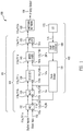
- Fig. 1 illustrates a block diagram of a digital to analog conversion system 100 in accordance with an embodiment of the disclosure.
- System 100 may be used to convert digital data signals into analog voltage signals in accordance with various techniques described herein.
- System 100 may be used on a variety of platforms, such as a land based platform, an airplane based platform, or a space based platform.
- system 100 may be provided in a satellite communications system.
- system 100 may be provided in a land based or airplane based radar system.
- system 100 includes a digital upconverter 101, a switching network 102, and a clock network 103.
- System 100 may be implemented as a high speed digital to analog conversion system where parallel digital data signals are received, frequency shifted and converted to an analog signal.
- Digital upconverter 101 may include, for example, a data path 104 and a synchronizer circuit 105.
- Data path 104 includes various digital components such as a mesochronous interface (MCI) circuit 110, a multiplexer circuit 120, a decoder circuit 130, and a mixer circuit 140.
- MCI mesochronous interface
- Components of data path 104 provide for clock domain transfer of mesochronous interface circuit input data bits 111a (e.g., MCI input data words) by MCI circuit 110, multiplexing of multiplexer input data bits 111b (e.g., plurality of parallel digital data words) by multiplexer circuit 120, decoding decoder input data bits 111c by decoder circuit 130, and frequency shifting mixer input data bits 111d (e.g., decoded parallel digital data bits) by mixer circuit 140.
- mesochronous interface circuit input data bits 111a e.g., MCI input data words
- multiplexer input data bits 111b e.g., plurality of parallel digital data words
- decoding decoder input data bits 111c by decoder circuit 130
- frequency shifting mixer input data bits 111d e.g., decoded parallel digital data bits
- data path 104 includes parallel data buses 113a-d, where each parallel data bus 113a-d includes data bits 111a-d, respectively.
- Data bits 111a-d, traveling through data path 104 may become time misaligned with each other after mixer circuit 140 due to differences in timing between logic state transitions at outputs of decoder circuit 130 (e.g., such as parallel digital data bits 238/239 of Fig. 2 ) and logic state transitions of conversion clock 145 during multiplication operations performed by mixer circuit 140.
- unintended glitches may occur at outputs of mixer circuit 140.
- synchronizer circuit 105 includes, for example, multiple data (D) flip flops where each D flip flop receives a corresponding one of a time misaligned data bits 111e on parallel data bus 113e to synchronize time misaligned data bits 111e and provide time aligned frequency shifted data bits 112a to switching network 102 on corresponding parallel data bus 114a.
- D data
- switching network 102 receives time aligned data bits 112a and converts time aligned data bits 112a to a single ended analog output signal 106.
- Switching network 102 may be implemented as multiple CMOS inverter circuits driving a resistor network, where each CMOS inverter circuit receives a corresponding time aligned frequency shifted data bit 112a. Each CMOS inverter circuit and resistor network configuration is determined based on a weighting of the associated time aligned data bit 112a. Weighting of each of the time aligned frequency shifted data bits 112a is assigned by decoder circuit 130.
- time aligned frequency shifted digital data bits 112a may be a combination of binary coded weighting and/or thermometer coded weighting, as discussed herein.
- clock network 103 includes a differential local clock 170, a dual-edge detector circuit 180, and a clock divider circuit 191.
- a differential local clock signal 175 is provided to dual-edge detector circuit 180 by differential local clock 170.
- Differential local clock signal 175 is converted to a single ended synchronizer clock signal 155 by dual-edge detector 180 having an integer multiple 156 of differential local clock signal 175 and provided to synchronizer circuit 105 at a synchronizer clock input 105a.
- integer multiple 156 of differential local clock signal 175 is a two times multiplier to provide a synchronizer clock signal frequency (2NFs) two times the differential local clock signal 175 to synchronize time misaligned data bits 111e at synchronizer circuit 105.
- clock divider circuit 191 receives single ended synchronizer clock signal 155 and divides synchronizer clock signal 155 by an integer value 146 to provide a conversion clock signal 145 at a mixer circuit clock input 140a. In some embodiments, clock divider circuit 191 is implemented to divide conversion clock signal 145 by an integer value 136 to provide a decoder clock signal 135 at a decoder clock input 130a. In various embodiments, clock divider circuit 191 is implemented to divide decoder clock signal 135 by an integer value 126 (e.g., integer value M) to provide a multiplexer clock signal 125 at a multiplexer clock input 120a.
- integer value 126 e.g., integer value M
- Multiplexer clock signal 125 may be provided to MCI circuit 110 at a MCI clock output 110a.
- MCI circuit 110 may receive an MCI clock signal 115 at a MCI clock input 110b.
- MCI clock signal 115 is mesochronous with multiplexer clock signal 125 operating at a frequency equivalent to the frequency of multiplexer clock signal 125.
- Other embodiments are also contemplated for a digital to analog conversion system 100 that provides for time alignment of time misaligned parallel data bits 111e and converting the time aligned frequency shifted digital data bits 112a to an analog output voltage signal 106.
- Fig. 4 illustrates a block diagram of a system 400 providing a differential output in accordance with an embodiment of the disclosure.
- system 400 may be implemented with a differential analog output signal 106a and 106b.
- system 400 provides for similar components used in system 100 to provide an analog output signal 106a, but in addition, includes components to provide a complementary analog output signal 106b.
- an additional mixer circuit 140b, synchronizer circuit 105b, and switching network 102b provide for complementary analog output signal 106b, where additional components operate in a manner substantially similar.
- conversion clock signal 145 is inverted at mixer circuit 140b clock input 141 to provide complementary analog output signal 106b.
- mixer circuits 140 and 140b are digital multipliers.
- mixer circuits 140 and 140b alternately multiply outputs of decoder circuit 130 (e.g., parallel digital data bits 111d) by +/- 1 (e.g., logic high/logic low).
- Additional mixer circuit 140b operates in opposite phase with respect to mixer circuit 140 to generate complementary analog output signal 106b.
- Fig. 2 illustrates various data bits 111a-e passing through parallel data paths 104 of system 100 in accordance with an embodiment of the disclosure.
- Fig. 2 illustrates processing of data bits 111a-e, as data bits 111a-e pass through digital components MCI 110, multiplexer circuit 120, decoder circuit 130, and mixer circuit 140.
- Parallel data bus 113a may include data bits 111a provided in parallel digital words A-D.
- digital words A-D e.g., MCI input data words
- MCI circuit 110 passes MCI input data bits 111a corresponding to parallel digital words A-D to multiplexer circuit 120 at the multiplexer clock rate (Fs/M) and multiplexer clock domain, as discussed herein.
- Fs/M multiplexer clock rate
- Multiplexer circuit 120 receives multiplexer input data bits 111b corresponding to parallel digital data words A-D (e.g., parallel digital data words 111b) on parallel data bus 113b and provides a serial data stream 208 corresponding to one bit 209 of each of the parallel digital words A-D (e.g., twelve data bits 111c of each of parallel digital words A-D) to decoder circuit 130 on parallel data bus 113c.
- multiplexer circuit 120 provides parallel digital data words A, B, C, D in serial order on parallel data bus 113c, where multiplexer circuit 120 selects serial digital data word order A, B, C, D, where digital data word A is clocked first followed by B, C, and D as shown in Fig. 2 .
- a 4:1 multiplexer is shown in Fig. 2 .
- other multiplexer configurations are possible in other embodiments.
- Decoder circuit 130 receives a parallel digital word 237 (e.g., one of parallel digital words A, B, C, or D) including decoder input data bits 111c on parallel data bus 113c.
- Data bits 111c include a first subset 234 (e.g., five data bits 111c) and a second subset 238 (e.g., seven data bits 111c).
- decoder circuit 130 converts first subset 234 to a second format 239.
- five binary coded data bits are converted to thirty-one thermometer coded (e.g., second format 239) data bits 111d to provide thirty-eight decoded parallel digital data bits 111d consisting of thirty-one thermometer coded data bits 111d and seven binary coded data bits 111d on parallel data bus 113d.
- One or more data bits 111d may be time misaligned with each other due to latencies 206 associated with logic operations performed in decoder circuit 130. It will be understood that other embodiments may include other types of coded data bits and decoder circuit may decode more or fewer data bits to one or more types of decoding configurations.
- Mixer circuit 140 receives decoded parallel digital data bits 111d (e.g., mixer input data bits) on parallel data bus 113d.
- decoded parallel digital data bits 111d may include a first subset 244 of data bits 111d (e.g., a first subset of thermometer coded data bits) and a second subset 249 of data bits 111d (e.g., a second subset of binary coded data bits).
- mixer input data bits 111d are frequency shifted using conversion clock signal 145.
- conversion clock signal 145 is substantially the same frequency as differential clock signal 175 frequency. In other embodiments, conversion clock signal 145 is an integer multiple of differential clock signal 175 frequency.
- Frequency shifted digital data bits 111e including frequency shifted first subset 244 and second subset 249 time misaligned data bits 111e are provided to synchronizer circuit 105 on parallel data bus 113e.
- One or more frequency shifted digital data bits 111e may be time misaligned with each other after multiplication operations performed by mixer circuit 140, as discussed herein.
- synchronizer circuit 105 receives frequency shifted first subset 244 and second subset 249 time misaligned data bits 111e on parallel data bus 113e. Data bits 111e are received from mixer circuit 140 of data path 104. Synchronizer circuit 105 performs operations to time align data bits 111e to provide time aligned frequency shifted digital data bits 112a on parallel data bus 114a, as discussed herein. In various embodiments, synchronizer circuit 105 performs time alignment of time misaligned data bits 111e at a synchronizer clock signal 155 frequency twice the differential clock signal 175 frequency to reduce system 100 susceptibility to process, temperature, and power supply variations. However, other frequency multiples of differential clock signal 175 are possible for synchronizer clock signal 155.
- Outputs (e.g., data bits 112a) of synchronizer circuit 105 are provided to switching network 102.
- Switching network 102 converts data bits 112a to analog output signal 106.
- Analog output signal 106 dominant spectral energy is centered around the frequency of conversion clock signal 145.
- Fig. 3 illustrates a process of operating system 100 in accordance with an embodiment of the disclosure.
- steps of Fig. 3 may be performed in an order different than that discussed herein.
- clock network 103 includes a differential local clock 170, a dual-edge detector circuit 180, and a clock divider circuit 191, as discussed herein.
- Dual-edge detector circuit 180 receives differential local clock signal 175 from differential local clock 170 to provide single ended synchronizer clock signal 155, as discussed herein.
- Fig. 7A illustrates a block diagram of a dual-edge detector circuit 180 in accordance with an embodiment of the disclosure.
- a positive differential clock signal 175a (e.g., LO_CLK_P) is provided to a first input port 787 of dual-edge detector circuit 180.
- a negative differential clock signal 175b (e.g., LO_CLK_N) is provided to a second input port 788 of dual-edge detector circuit 180.
- Positive and negative differential clock signals 175a and 175b includes resistor feedback amplifiers 776a and 776b, respectively.
- Dual-edge detector circuit 180 includes multiple logic gates 789 to perform logic operations in response to positive differential clock signal 175a and negative differential clock signal 175b to form synchronizer clock signal 155 (e.g., 2NFs Clock), where synchronizer clock signal 155 is a single ended clock signal 757 having a frequency (2NFs) that is twice the frequency of differential clock signal 175 (NFs).
- synchronizer clock signal 155 e.g., 2NFs Clock
- Fig. 7B illustrates a timing diagram 702 of a dual-edge detector circuit 180 in accordance with an embodiment of the disclosure.
- timing diagram 702 illustrates a relation between synchronizer clock signal 155, and positive differential clock signal 175a, and negative differential clock signal 175b.
- Fig. 7B shows that a synchronizer clock first pulse 756a is formed in response to a rising edge of positive differential clock signal 175a, and/or a falling edge of negative differential clock signal 175b.
- a synchronizer clock second pulse 756b is formed in response to a falling edge of positive differential clock signal 175a, and/or a rising edge of negative differential clock signal 175b.
- synchronizer clock signal 155 implements a frequency twice (e.g., an integer multiple of) the frequency of differential local clock signal 175.
- clock divider circuit 191 receives single ended synchronizer clock signal 155 and divides synchronizer clock signal 155 by an integer value 146 to provide conversion clock signal 145, as discussed herein.
- Clock divider circuit 191 is implemented to divide conversion clock signal 145 by an integer value 136 to provide decoder clock signal 135, as discussed herein.
- Clock divider circuit 191 is implemented to divide decoder clock signal 135 by an integer value 126 (e.g., integer value M) to provide multiplexer clock signal 125, as discussed herein.
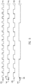
- Fig. 5 illustrates a timing diagram of clock network 103 in accordance with an embodiment of the disclosure.
- a relation between synchronizer clock signal 155, conversion clock signal 145, decoder clock signal 135, and multiplexer clock signal 125 is shown.
- integer multiple 146 is equal to one
- integer multiple 126 is equal to four.
- differential local clock signal 175 (not shown) is 3.2 Gsps.
- conversion clock signal 145, and decoder clock signal 135 are 3.2 Gsps
- multiplexer clock signal 125 is 0.8 Gsps.
- decoder clock signal 135 is configured to operate at a predefined sample rate Fs. As shown in Fig.
- synchronizer clock signal 155 is twice the differential local clock signal 175, or 6.4 Gsps.
- time misaligned data bits 111e are sampled at 6.4 Gsps by synchronizer circuit 105. Sampling by synchronizer circuit 105 at synchronizer clock signal 155 sample rate facilitates consistent output power over data frequency and temperature variations at the switching network output, as discussed herein. It is understood the timing diagram of Fig. 5 provides a nonlimiting embodiment of the present disclosure. Other timing diagrams with other clock rates are possible in other embodiments.
- mesochronous interface (MCI) circuit 110 receives input data bits 111a corresponding to parallel digital data words A-D (e.g., MCI input data words) on parallel data bus 113a.
- MCI receives multiplexer clock signal 125 at MCI clock output 110b and MCI clock signal 115 at MCI clock input 110a where MCI clock signal 115 is mesochronous with multiplexer clock signal 125, as discussed herein.
- MCI input data bits 111a are clocked by MCI clock signal 115 to receive MCI input data bits 111a at MCI 110.
- MCI 110 converts clock domain of MCI input data bits 111a using multiplexer clock signal 125 to clock multiplexer input data bits 111b to multiplexer circuit 120.
- Multiplexer input data bits 111b correspond to parallel digital data words A-D.
- multiplexer circuit 120 receives multiplexer input data bits 111b corresponding to parallel digital data words A-D on parallel data bus 113b. Multiplexer circuit 120 combines multiplexer input data bits 111b to provide decoder input data bits 111c clocked by decoder clock signal 135 to decoder circuit 130. In this regard, multiplexer circuit 120 selects a corresponding one of parallel digital data words A-D, where one of parallel digital data words A-D are selected to be provided to decoder circuit 130. Subsequent clock cycles provide the remainder of parallel digital data words A-D.
- the order of clocking parallel digital data words is A, B, C, D, where digital data word A is clocked first followed by B, C, and D. Clocking digital data word A-D using decoder clock signal 135 provides for an equivalent throughput of clocking parallel digital data words A-D using multiplexer clock signal 125.
- decoder circuit 130 receives decoder input data bits 111c including a first subset 234 and a second subset 238, where each subset 234 and 238 are a first format (e.g, such as binary coded data bits).
- first format e.g, such as binary coded data bits
- second format 239 e.g., such as thermometer coded data bits
- a first subset 244 of decoded data bits 111d are provided to mixer circuit 140.
- second subset 249 of data bits 111d are passed to mixer circuit 140 without decoding (e.g., remaining binary coded data bits), as discussed herein.
- mixer circuit 140 receives mixer input data bits 111d including first subset data bits 244 and second subset data bits 249.
- Fig. 6A illustrates a block diagram of a mixer circuit 140 in accordance with an embodiment of the disclosure. Referring to Fig.
- mixer circuit 140 includes multiple exclusive OR logic components 643(1) through 643(n) receiving conversion clock signals 145(1) through 145(n) (e.g., NFs Clock) and decoded parallel digital data bits 111(d)(1) (e.g., Mixer_in(1)) through 111(d)(n) (e.g., Mixer_in (n)), and providing frequency shifted digital data bits 111(e(1) (e.g., Mixer_out(1)) through 111(e)(n) (e.g., Mixer_out(n).
- each mixer exclusive OR circuit 643 combines one data bit 111d and one conversion clock signal 145 to provide a corresponding frequency shifted digital data bit 111e.
- mixer circuit 140 may include multiplexers or other complex logic gates to implement operational functionality of mixer circuit 140.
- Fig. 6B illustrates a timing diagram of a mixer circuit 140 in accordance with an embodiment of the disclosure.
- timing diagram provides mixer input data bits 111(d)(1) (e.g., Mixer_in), conversion clock signal 145(1) (e.g., NFs Clock), and data signal 603 of mixer output data bits 111(e)(1) (e.g., Mixer_out).
- mixer input data bits 111(d)(1) e.g., Mixer_in
- conversion clock signal 145(1) e.g., NFs Clock
- data signal 603 of mixer output data bits 111(e)(1) e.g., Mixer_out
- logic operations are performed on data bits 111(d)(1) and clock signal 145(1) to provide data bits 111(e)(1).
- data signal 603 of data bits 111(e)(1) transitions high when data bits 111(d)(1) and clock signal 145(1) are at different logic states, effectively multiplying data bits 111(d)(1) with conversion clock signal 145 to shift the energy of data bits 111(d)(1) to center around conversion clock signal frequency NFs.
- frequency shifted digital data bits 111e may become time misaligned with each other due to time misalignment associated with logic state transitions of each of the decoded parallel digital data bits 111(d) and logic state transitions of the conversion clock signal 145. Additionally, data bits 111e may have undesirable glitches 605 due to time misalignment of edges between mixer input data bits 111(d)(1) and conversion clock signal 145(1).
- Fig. 6C illustrates a schematic diagram of a mixer circuit 602 (e.g., a digital mixer cell) in accordance with an embodiment of the disclosure.
- schematic diagram of mixer circuit 602 provides for a single mixer input data bit 111(d)(1) (e.g., Mixer_in), conversion clock signal 145(1) (e.g., NFs Clock), and mixer output data bit 111(e)(1) (e.g., Mixer_out).
- mixer circuit 140 includes mixer circuit 602 for each data bit 111d.
- the number of mixer circuits 602 required may vary based on the number of decoded data bits 244 and undecoded data bits 249 of data bits 111d provided by decoder circuit 130.
- logic operations are performed on each of mixer inputs data bits 111d with conversion clock signal 145 to provide possible time misaligned data bits 111e to synchronizer circuit 105.
- mixer circuit 602 is implemented as a CMOS voltage mode circuit 636.
- Static power is reduced as there are no constant current sources included within CMOS voltage mode circuit 636.
- power is dissipated primarily during data and clock logic state transitions, resulting in a reduction in power dissipation.
- voltage mode topology provides for reduced power dissipation and power consumption important in space based applications.
- Fig. 8A illustrates a schematic diagram of a synchronizer circuit 105 in accordance with an embodiment of the disclosure. Referring now to Fig.
- FIG. 8A schematic diagram of synchronizer circuit 105 provides for single synchronizer input data bit 111(e)(1) (e.g., Sync_in) at a synchronizer circuit data input 804(a), a synchronizer clock signal 855(a) (e.g., 2NFs Clock) at a synchronizer circuit clock input 806(a), and synchronizer output data bit 112(a)(1) (e.g., Sync_out) at a synchronizer circuit data output 810(a).
- synchronizer input data bit 111(e)(1) e.g., Sync_in
- a synchronizer clock signal 855(a) e.g., 2NFs Clock
- synchronizer output data bit 112(a)(1) e.g., Sync_out
- synchronizer circuit 105 is implemented as a data (D) flip flop circuit 805, where D flip flop circuit 805 latches time misaligned data bit 111(e)(1) in response to synchronizer clock signal 855a to provide time aligned frequency shifted digital data bit 112(a)(1) at synchronizer circuit data output 810(a).
- time misaligned data bit 111(e)(1) is held at synchronizer circuit data input 804(a) until a rising edge of single ended synchronizer clock signal 855a is provided at synchronizer circuit clock input 806(a) to provide time aligned data bit 112(a)(1) to switching network 102.
- synchronizer circuit 105 includes multiple (D) flip flop circuits 805, where each (D) flip flop circuit 805 is provided for each data bit 111(e)(1) through 111(e)(n).
- the number of (D) flip flop circuits 805 required may vary based on the number of decoded 244 and undecoded 249 time misaligned data bits 111e provided by mixer circuit 140.
- (D) flip flop circuit 805 and synchronizer circuit 105 is implemented as a CMOS voltage mode circuit 836.
- synchronizer clock signal 155 is fanned out to each D flip flop circuit 805.
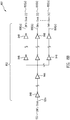
- Fig. 8B illustrates a schematic diagram of a synchronizer clock distribution circuit 807 in accordance with an embodiment of the disclosure. Referring now to Fig. 8B , synchronizer clock distribution circuit 807 provides for a clock distribution of synchronizer clock signal 155 to each of D flip flop circuits 805 of synchronizer circuit 105.
- clock distribution path 852 provides for an identical number of inverter stages 848 for each synchronizer clock signal 855a-n along the signal path from synchronizer clock input 105a to each corresponding synchronizer circuit clock input 806a-n.
- clock distribution path 852 provides for an identical number of inverter stages 848 for each synchronizer clock signal 855a-n along the signal path from synchronizer clock input 105a to each corresponding synchronizer circuit clock input 806a-n.
- simultaneous rising edges of synchronizer clock signals 855a-n is provided at corresponding clock inputs 806a-n of corresponding D flip flop circuit 805a-n to simultaneously clock time misaligned data bits 111(e)(1) through 111(e)(n) to provide time aligned data bits 112 (a) (1) through 112 (a) (n) at corresponding D flip flop circuit data outputs 810a-n.
- synchronizer circuit 105 provides time aligned data bits 112a to switching network 102.
- Fig. 9 illustrates timing diagrams of a mixer circuit 140 and a synchronizer circuit 105 in accordance with embodiments of the disclosure.
- Figure 9 shows the timing functions for one data bit 111e in the mixer circuit 140 and one data bit 112a in the synchronizer circuit 105 to illustrate how glitches 605 may occur at the mixer output and how the synchronizer circuit 105 removes glitches 605 in addition to alignment of the multiple data bits 111e using the synchronizer clock signal 155.
- timing diagrams provide mixer circuit 140, mixer input data bits 111(d)(1) (e.g., Mixer_in), conversion clock signal 145(1) (e.g., NFs Clock), and data signal 603 of mixer output data bits 111(e)(1) (e.g., Mixer_out). Additionally timing diagrams provide synchronizer circuit 105, synchronizer input data bits 111(e)(1) (e.g., Sync_in), synchronizer clock signal 855(a) (e.g., 2NFs Clock), and data signal 903 of synchronizer output data bits 112(a)(1) (e.g., Sync_out). As shown, Fig.
- Frequency shifted digital data bits 111(e)(1) are provided to synchronizer circuit 105, where data bits 111(e)(1) are sampled to provide time aligned frequency shifted digital data bits 112(a)(1) and to remove glitches 605.
- Fig. 9 shows synchronizer clock signal 855(a) samples synchronizer input data bits 111(e)(1) to provide for accurate, high speed time alignment of data bits 111(e)(1), as discussed herein.
- conversion clock signal 145(1) frequency shifts data bits 111(e)(1) at a conversion rate of 3.2 Gsps.
- Synchronizer clock signal 855(a) samples data bits 111(e)(1) at a synchronizer clock rate of 6.4 Gsps, twice the mixer circuit sampling rate.
- Synchronizer circuit 105 provides for adaptability to modify sampling rates without the need to re-tune or re-design system 100.
- time aligned frequency shifted digital data bits 112a are converted to analog voltage signals and summed to provide analog output signal 106.
- switching network 102 receives time aligned data bits 112a and converts time aligned data bits 112a to corresponding analog voltage signals, as discussed herein.
- Fig. 10 illustrates a schematic diagram of a switching network circuit 102 in accordance with an embodiment of the disclosure.
- switching network 102 may be implemented as multiple CMOS inverter circuits driving a resistor network (e.g., such as thermometer weighted circuits 1013 and binary weighted circuits 1015), where each CMOS inverter circuit resistor network receives a corresponding time aligned data bit 112a based on an assigned weighting of data bit 112a and converts the corresponding digital data bit 112a to a corresponding voltage signal 1006. Voltage signals 1006 are summed at a summing node 1008 and provided as analog output signal 106. It will be appreciated that the number of voltage signals 1006 and/or resistors 1023/1025 may vary based on the number of time aligned frequency shifted digital data bits 112a.
- resistor network e.g., such as thermometer weighted circuits 1013 and binary weighted circuits 1015
- each of a multiple of thermometer weighted circuits 1013 of switching network 102 includes a series pair of inverter circuits 1021 and a fixed value resistor 1023.
- each of thermometer decoded data bits 112(a)(1) through 112(a)(31) are weighted equally and a substantially equivalent voltage at output 1006(1) through 1006(31) are provided to summing node 1008 by each of thermometer weighted circuits 1013.
- each of a multiple of binary weighted circuits 1015 of switching network 102 includes series pair of inverter circuits 1021 and a variable value resistor 1025.
- a value of variable resistor 1025 for each data bit 112(a)(32) through 112(a)(38) is identified based on a weight of binary data bits 112(a)(32) through 112(a)(38).
- data bit 112(a)(38) may be a less significant bit than data bit 112(a)(31).
- voltage signal at output 1006(38) corresponding to data bit 112(a)(38) would be less than voltage signal at output 1006(31) corresponding to data bit 112(a)(31).
- variable resistor 1025 coupled to output 1006(38) would be a larger value than variable resistor 1025 coupled to output 1006(31).
- each of binary undecoded data bits 112(32) through 112(a)(38) are weighted proportional to their bit significance (e.g., least significant to most significant) and corresponding voltages are provided at outputs 1006(31) through 1006(38) to summing node 1008.
- switching network 102 is implemented as a CMOS voltage mode circuit 1036 to provide for low power dissipation and power consumption.
- switching network 102 includes bias resistors R39 and R40.
- Bias resistor R39 is coupled to voltage source VDDA on a first end and summing node 1008 on a second end.
- Bias resistor R40 is coupled to GNDA (e.g., direct current (DC) ground) on a first end and summing node 1008 on a second end.
- the resistance of R39 is substantially equal to the resistance of R40.
- Bias resistors R39 and/or R40 set a bias voltage 1010 of analog output signal 106.
- an output impedance of analog output signal 106 is fixed by the combination of bias resistors R39/R40 and resistors 1023/1025.
- Fig. 11 illustrates a plot 1100 of signal energy versus frequency for a digital to analog upconverter in accordance with an embodiment of the disclosure.
- plot 1100 shows dominant spectral energy 1106 of analog output signal 106 centered at a frequency of approximately 3.2 GHz, between second Nyquist 1115 and third Nyquist 1125.
- the sampling frequency (Fs) used by the decoder circuit 130 is 3.2GHz and digital data processed by the decoder circuit 130 has a frequency of 100MHz (e.g., data signal frequency), as shown by signal 1130 on plot 1100.
- the mixer rate (NFs) is also 3.2GHz and the digital mixer circuit 140 shifts more of the energy in the digital data to 3.1GHz and 3.3GHz (e.g., mixer rate +/- data signal frequency), as shown by signals 1106 on plot 1100. Harmonics having lower power occur at multiples of the mixer rate (e.g., 6.4GHz and 9.6GHz), as shown by signals 1135 and signals 1140 on plot 1100.
- the synchronization rate is 6.4GHz and cannot be discerned in spectral energy plot 1100.
- providing system 100 in accordance with various embodiments set forth herein may provide for adaptable and high speed digital to analog upconversion of a plurality of parallel digital data bits to an analog output voltage signal.
- an adaptable, high speed and high resolution digital to analog conversion may be implemented for satellite communications system.
- various embodiments provided by the present disclosure can be implemented using hardware, software, or combinations of hardware and software. Also where applicable, the various hardware components and/or software components set forth herein can be combined into composite components comprising software, hardware, and/or both without departing from the spirit of the present disclosure. Where applicable, the various hardware components and/or software components set forth herein can be separated into sub-components comprising software, hardware, or both without departing from the spirit of the present disclosure. In addition, where applicable, it is contemplated that software components can be implemented as hardware components, and vice-versa.
- Software in accordance with the present disclosure can be stored on one or more non-transitory machine readable mediums. It is also contemplated that software identified herein can be implemented using one or more general purpose or specific purpose computers and/or computer systems, networked and/or otherwise. Where applicable, the ordering of various steps described herein can be changed, combined into composite steps, and/or separated into sub-steps to provide features described herein.
Landscapes
- Engineering & Computer Science (AREA)
- Theoretical Computer Science (AREA)
- Power Engineering (AREA)
- Computer Networks & Wireless Communication (AREA)
- Signal Processing (AREA)
- Electronic Switches (AREA)
- Analogue/Digital Conversion (AREA)
- Synchronisation In Digital Transmission Systems (AREA)
- Semiconductor Integrated Circuits (AREA)
Abstract
Description
- The present invention relates generally to digital to analog conversion and, more particularly, to high speed and low power digital to analog upconverter implementations. In the field of high speed digital to analog conversion systems, particularly in satellite applications, there is an ongoing effort to include frequency upconversion in the digital domain by implementing higher speed digital to analog up converter circuits with integrated digital mixer circuits. However, time misalignment of digital data signals after the mixer circuit is a concern to achieving high speed upconversion system performance. The time misalignments are due in part to differences between data signal logic transitions and conversion clock transitions at the inputs of the digital mixer circuit.
- Various conventional techniques attempt to reduce the time misalignments. For example, current mode logic circuit topologies may be used to reduce a portion of the time misalignments, but have the disadvantage of increasing power dissipation without significant improvement to system performance. Another conventional technique to address time misalignments may be to manually adjust physical signal paths in the digital to analog upconverter, but this step may be time consuming and may not be feasible if the digital to analog upconverter is used for different applications (e.g., frequency upconversion at different data rates).
- Systems and methods are disclosed herein in accordance with one or more embodiments that provide an improved approach to high speed digital to analog upconversion. A high speed digital to analog conversion system provides for converting a plurality of parallel digital data bits to an analog output voltage signal. In one example, a digital to analog upconverter includes various digital circuit components to perform logic operations and convert the frequency of incoming parallel digital data bits from a lower range to a higher range, where the parallel digital data bits become time misaligned with each other after the frequency conversion due to differences in logic states between a frequency conversion clock signal and each of the data bits. Parallel digital words corresponding to the time misaligned data bits are passed to a synchronizer circuit. The synchronizer circuit time aligns the parallel digital data bits and provides the time aligned parallel digital data bits to a switching network where the data bits are converted to an analog voltage signal.
- In one embodiment, a system includes a decoder circuit configured to receive a plurality of decoder input data bits and provide a plurality of decoded parallel digital data bits, wherein the decoder circuit operates at a predefined sample rate; a mixer circuit coupled to the decoder circuit and configured to combine each of the decoded parallel digital data bits with a conversion clock signal to provide frequency shifted digital data bits, wherein the frequency shifted digital data bits are time misaligned with each other; a synchronizer circuit coupled to the mixer circuit comprising a synchronizer clock signal and configured to time align the frequency shifted digital data bits in response to the synchronizer clock signal; and a switching network coupled to the synchronizer circuit and configured to generate an analog output signal in response to the time aligned frequency shifted digital data bits.
- In another embodiment, a method includes receiving, by a decoder circuit, a plurality of decoder input data bits; providing, by the decoder circuit, a plurality of decoded parallel digital data bits, wherein the decoder circuit operates at a predefined sample rate; combining, by a mixer circuit coupled to the decoder circuit, each of the decoded parallel digital data bits with a conversion clock signal to provide frequency shifted digital data bits, wherein the frequency shifted digital data bits are time misaligned with each other; aligning, by a synchronizer circuit coupled to the mixer circuit, the frequency shifted digital data bits in response to a synchronizer clock signal; and generating, by a switching network coupled to the synchronizer circuit, an analog output signal in response to the time aligned frequency shifted digital data bits.
- The scope of the invention is defined by the claims, which are incorporated into this section by reference. A more complete understanding of embodiments of the invention will be afforded to those skilled in the art, as well as a realization of additional advantages thereof, by a consideration of the following detailed description of one or more embodiments. Reference will be made to the appended sheets of drawings that will first be described briefly.
-
-
Fig. 1 illustrates a block diagram of a digital to analog conversion system in accordance with an embodiment of the disclosure. -
Fig. 2 illustrates various data bits passing through parallel data paths of a digital to analog conversion system in accordance with an embodiment of the disclosure. -
Fig. 3 illustrates a process of operating a digital to analog conversion system in accordance with an embodiment of the disclosure. -
Fig. 4 illustrates a block diagram of a digital to analog conversion system providing a differential output in accordance with an embodiment of the disclosure. -
Fig. 5 illustrates a timing diagram of a clock network in accordance with an embodiment of the disclosure. -
Fig. 6A illustrates a block diagram of a mixer circuit in accordance with an embodiment of the disclosure. -
Fig. 6B illustrates a timing diagram of a mixer circuit in accordance with an embodiment of the disclosure. -
Fig. 6C illustrates a schematic diagram of a mixer circuit in accordance with an embodiment of the disclosure. -
Fig. 7A illustrates a block diagram of a dual-edge detector circuit in accordance with an embodiment of the disclosure. -
Fig. 7B illustrates a timing diagram of a dual-edge detector circuit in accordance with an embodiment of the disclosure. -
Fig. 8A illustrates a schematic diagram of a synchronizer circuit in accordance with an embodiment of the disclosure. -
Fig. 8B illustrates a schematic diagram of a synchronizer clock distribution circuit in accordance with an embodiment of the disclosure. -
Fig. 9 illustrates timing diagrams of a mixer circuit and a synchronizer circuit in accordance with an embodiment of the disclosure. -
Fig. 10 illustrates a schematic diagram of a switching network circuit in accordance with an embodiment of the disclosure. -
Fig. 11 illustrates a plot of signal energy versus frequency for a digital to analog upconverter in accordance with an embodiment of the disclosure. - Various implementations of a digital to analog frequency upconversion system are provided to reduce time misalignment of parallel digital data bits with each other before conversion to an analog signal. The digital to analog frequency upconversion system includes a decoder, a mixer, a synchronizer, a switching network, and a clock network used to convert parallel digital data bits to an analog voltage. In various embodiments, the digital to analog upconverter receives the parallel digital data bits from an external source such as a digital signal processor (DSP). In some embodiments, the digital to analog upconverter includes data paths including various digital components to perform logic operations on the parallel digital data bits comprised of multiplexing, decoding, and multiplying, where the parallel digital data bits become time misaligned with each other after the multiplication step due to differences in logic state transitions in decoding outputs relative to logic state transitions in a multiplying clock (e.g., such as
conversion clock signal 145 ofFig. 1 ). - In various embodiments, the digital to analog upconverter includes a synchronizer circuit to perform time alignment of the time misaligned parallel digital data bits. In this regard, the synchronizer circuit provides for time alignment of the digital data bits prior to the switching network. Time alignment of the digital data bits at the input to the switching network is important to provide for high performance digital to analog conversion. In particular, the synchronizer circuit facilitates consistent output power over data frequency and temperature variations at the switching network output to maximize an effective number of bits, a key performance metric for a digital to analog converter.
- In various embodiments, the synchronizer circuit is implemented as parallel flip flops, where each flip flop receives one of the parallel time misaligned digital data bits. A synchronizer clock signal is provided to each flip flop to sample the time misaligned data bit. In some embodiments, each flip flop may be a data (D) flip flop implemented to sample the data bit in response to the synchronizer clock signal. In some embodiments, the time misaligned data bits are sampled at twice the rate of the frequency conversion rate to eliminate any glitches or misalignments in the digital data bits.
- In various embodiments, the clock network is implemented as a differential local clock, a dual-edge detector circuit, and a clock divider circuit. The differential local clock serves as a master clock and a differential local clock signal is provided to the dual-edge detector. The dual-edge detector converts the differential signal to a single ended synchronizer clock signal. In some embodiments, the synchronizer clock signal is a single ended pulsed output clock signal, where each pulsed output is generated at a rising and a falling edge of the differential clock signal to provide a frequency twice the differential clock signal frequency. Significantly, the synchronizer circuit provides for adaptability to vary the master differential local clock signal and maintain high speed performance without the need to manually re-tune the digital data paths.
- The clock divider circuit is implemented to divide the single ended synchronizer clock signal to provide for a conversion clock signal, a decoder clock signal, and a multiplexer clock signal. In this regard, the digital to analog upconversion system is implemented with single ended clock signals to provide for a reduction in power dissipation and power consumption. In particular, the digital to analog upconversion system uses standard digital CMOS process fabrication techniques and single-ended circuit topologies operating in voltage mode to reduce overall size and power. For example, each of the circuit blocks consume substantially no bias power and primarily dissipate power during logic state transitions only.
-
Fig. 1 illustrates a block diagram of a digital toanalog conversion system 100 in accordance with an embodiment of the disclosure.System 100 may be used to convert digital data signals into analog voltage signals in accordance with various techniques described herein.System 100 may be used on a variety of platforms, such as a land based platform, an airplane based platform, or a space based platform. In one embodiment,system 100 may be provided in a satellite communications system. In another embodiment,system 100 may be provided in a land based or airplane based radar system. - In one embodiment,
system 100 includes adigital upconverter 101, aswitching network 102, and aclock network 103.System 100 may be implemented as a high speed digital to analog conversion system where parallel digital data signals are received, frequency shifted and converted to an analog signal. -
Digital upconverter 101 may include, for example, adata path 104 and asynchronizer circuit 105.Data path 104 includes various digital components such as a mesochronous interface (MCI)circuit 110, amultiplexer circuit 120, adecoder circuit 130, and amixer circuit 140. Components ofdata path 104 provide for clock domain transfer of mesochronous interface circuitinput data bits 111a (e.g., MCI input data words) byMCI circuit 110, multiplexing of multiplexerinput data bits 111b (e.g., plurality of parallel digital data words) bymultiplexer circuit 120, decoding decoderinput data bits 111c bydecoder circuit 130, and frequency shifting mixerinput data bits 111d (e.g., decoded parallel digital data bits) bymixer circuit 140. - In some embodiments,
data path 104 includesparallel data buses 113a-d, where eachparallel data bus 113a-d includesdata bits 111a-d, respectively.Data bits 111a-d, traveling throughdata path 104 may become time misaligned with each other aftermixer circuit 140 due to differences in timing between logic state transitions at outputs of decoder circuit 130 (e.g., such as paralleldigital data bits 238/239 ofFig. 2 ) and logic state transitions ofconversion clock 145 during multiplication operations performed bymixer circuit 140. In some embodiments, unintended glitches may occur at outputs ofmixer circuit 140. - In one embodiment,
synchronizer circuit 105 includes, for example, multiple data (D) flip flops where each D flip flop receives a corresponding one of a timemisaligned data bits 111e onparallel data bus 113e to synchronize timemisaligned data bits 111e and provide time aligned frequency shifteddata bits 112a to switchingnetwork 102 on correspondingparallel data bus 114a. - In some embodiments, switching
network 102 receives time aligneddata bits 112a and converts time aligneddata bits 112a to a single endedanalog output signal 106.Switching network 102 may be implemented as multiple CMOS inverter circuits driving a resistor network, where each CMOS inverter circuit receives a corresponding time aligned frequency shifted data bit 112a. Each CMOS inverter circuit and resistor network configuration is determined based on a weighting of the associated time aligned data bit 112a. Weighting of each of the time aligned frequency shifteddata bits 112a is assigned bydecoder circuit 130. In some embodiments, time aligned frequency shifteddigital data bits 112a may be a combination of binary coded weighting and/or thermometer coded weighting, as discussed herein. - In some embodiments,
clock network 103 includes a differentiallocal clock 170, a dual-edge detector circuit 180, and aclock divider circuit 191. A differentiallocal clock signal 175 is provided to dual-edge detector circuit 180 by differentiallocal clock 170. Differentiallocal clock signal 175 is converted to a single endedsynchronizer clock signal 155 by dual-edge detector 180 having an integer multiple 156 of differentiallocal clock signal 175 and provided tosynchronizer circuit 105 at asynchronizer clock input 105a. In some embodiments, integer multiple 156 of differentiallocal clock signal 175 is a two times multiplier to provide a synchronizer clock signal frequency (2NFs) two times the differentiallocal clock signal 175 to synchronize timemisaligned data bits 111e atsynchronizer circuit 105. - In some embodiments,
clock divider circuit 191 receives single endedsynchronizer clock signal 155 and dividessynchronizer clock signal 155 by aninteger value 146 to provide aconversion clock signal 145 at a mixercircuit clock input 140a. In some embodiments,clock divider circuit 191 is implemented to divideconversion clock signal 145 by an integer value 136 to provide adecoder clock signal 135 at adecoder clock input 130a. In various embodiments,clock divider circuit 191 is implemented to dividedecoder clock signal 135 by an integer value 126 (e.g., integer value M) to provide amultiplexer clock signal 125 at amultiplexer clock input 120a. -
Multiplexer clock signal 125 may be provided toMCI circuit 110 at a MCI clock output 110a.MCI circuit 110 may receive anMCI clock signal 115 at aMCI clock input 110b. In some embodiments,MCI clock signal 115 is mesochronous withmultiplexer clock signal 125 operating at a frequency equivalent to the frequency ofmultiplexer clock signal 125. Other embodiments are also contemplated for a digital toanalog conversion system 100 that provides for time alignment of time misalignedparallel data bits 111e and converting the time aligned frequency shifteddigital data bits 112a to an analogoutput voltage signal 106. - For example,
Fig. 4 illustrates a block diagram of asystem 400 providing a differential output in accordance with an embodiment of the disclosure. As shown inFig. 4 ,system 400 may be implemented with a differentialanalog output signal system 400 provides for similar components used insystem 100 to provide ananalog output signal 106a, but in addition, includes components to provide a complementaryanalog output signal 106b. As shown inFig. 4 , anadditional mixer circuit 140b,synchronizer circuit 105b, and switchingnetwork 102b provide for complementaryanalog output signal 106b, where additional components operate in a manner substantially similar. Additionally,conversion clock signal 145 is inverted atmixer circuit 140b clock input 141 to provide complementaryanalog output signal 106b. In particular,mixer circuits mixer circuits digital data bits 111d) by +/- 1 (e.g., logic high/logic low).Additional mixer circuit 140b operates in opposite phase with respect tomixer circuit 140 to generate complementaryanalog output signal 106b. Althoughsystem 100 will be discussed, various embodiments provided by the present disclosure apply tosystem 400 where applicable. -
Fig. 2 illustratesvarious data bits 111a-e passing throughparallel data paths 104 ofsystem 100 in accordance with an embodiment of the disclosure.Fig. 2 illustrates processing ofdata bits 111a-e, asdata bits 111a-e pass throughdigital components MCI 110,multiplexer circuit 120,decoder circuit 130, andmixer circuit 140.Parallel data bus 113a may includedata bits 111a provided in parallel digital words A-D. In some embodiments, digital words A-D (e.g., MCI input data words) each contain twelveparallel data bits 111a.MCI circuit 110 passes MCIinput data bits 111a corresponding to parallel digital words A-D tomultiplexer circuit 120 at the multiplexer clock rate (Fs/M) and multiplexer clock domain, as discussed herein. -
Multiplexer circuit 120 receives multiplexerinput data bits 111b corresponding to parallel digital data words A-D (e.g., paralleldigital data words 111b) onparallel data bus 113b and provides aserial data stream 208 corresponding to onebit 209 of each of the parallel digital words A-D (e.g., twelvedata bits 111c of each of parallel digital words A-D) todecoder circuit 130 onparallel data bus 113c. In this regard,multiplexer circuit 120 provides parallel digital data words A, B, C, D in serial order onparallel data bus 113c, wheremultiplexer circuit 120 selects serial digital data word order A, B, C, D, where digital data word A is clocked first followed by B, C, and D as shown inFig. 2 . By way of example, a 4:1 multiplexer is shown inFig. 2 . However, other multiplexer configurations are possible in other embodiments. -
Decoder circuit 130 receives a parallel digital word 237 (e.g., one of parallel digital words A, B, C, or D) including decoderinput data bits 111c onparallel data bus 113c.Data bits 111c include a first subset 234 (e.g., fivedata bits 111c) and a second subset 238 (e.g., sevendata bits 111c). In some embodiments,decoder circuit 130 convertsfirst subset 234 to asecond format 239. In some embodiments, five binary coded data bits (e.g., first subset 234) are converted to thirty-one thermometer coded (e.g., second format 239)data bits 111d to provide thirty-eight decoded paralleldigital data bits 111d consisting of thirty-one thermometer codeddata bits 111d and seven binarycoded data bits 111d onparallel data bus 113d. One ormore data bits 111d may be time misaligned with each other due tolatencies 206 associated with logic operations performed indecoder circuit 130. It will be understood that other embodiments may include other types of coded data bits and decoder circuit may decode more or fewer data bits to one or more types of decoding configurations. -
Mixer circuit 140 receives decoded paralleldigital data bits 111d (e.g., mixer input data bits) onparallel data bus 113d. In some embodiments, decoded paralleldigital data bits 111d may include afirst subset 244 ofdata bits 111d (e.g., a first subset of thermometer coded data bits) and asecond subset 249 ofdata bits 111d (e.g., a second subset of binary coded data bits). In some embodiments, mixerinput data bits 111d are frequency shifted usingconversion clock signal 145. In some embodiments,conversion clock signal 145 is substantially the same frequency asdifferential clock signal 175 frequency. In other embodiments,conversion clock signal 145 is an integer multiple ofdifferential clock signal 175 frequency. Frequency shifteddigital data bits 111e including frequency shiftedfirst subset 244 andsecond subset 249 timemisaligned data bits 111e are provided tosynchronizer circuit 105 onparallel data bus 113e. One or more frequency shifteddigital data bits 111e may be time misaligned with each other after multiplication operations performed bymixer circuit 140, as discussed herein. - In one embodiment,
synchronizer circuit 105 receives frequency shiftedfirst subset 244 andsecond subset 249 timemisaligned data bits 111e onparallel data bus 113e.Data bits 111e are received frommixer circuit 140 ofdata path 104.Synchronizer circuit 105 performs operations to time aligndata bits 111e to provide time aligned frequency shifteddigital data bits 112a onparallel data bus 114a, as discussed herein. In various embodiments,synchronizer circuit 105 performs time alignment of timemisaligned data bits 111e at asynchronizer clock signal 155 frequency twice thedifferential clock signal 175 frequency to reducesystem 100 susceptibility to process, temperature, and power supply variations. However, other frequency multiples ofdifferential clock signal 175 are possible forsynchronizer clock signal 155. Outputs (e.g.,data bits 112a) ofsynchronizer circuit 105 are provided to switchingnetwork 102.Switching network 102converts data bits 112a toanalog output signal 106.Analog output signal 106 dominant spectral energy is centered around the frequency ofconversion clock signal 145. -
Fig. 3 illustrates a process ofoperating system 100 in accordance with an embodiment of the disclosure. In describing the process ofoperating system 100, reference may be made to one or more ofFigs 4-11 . Furthermore, steps ofFig. 3 may be performed in an order different than that discussed herein. - In
block 305, the process begins withoperating clock network 103 to provide clock signals to components ofsystem 100. In this regard,clock network 103 includes a differentiallocal clock 170, a dual-edge detector circuit 180, and aclock divider circuit 191, as discussed herein. Dual-edge detector circuit 180 receives differentiallocal clock signal 175 from differentiallocal clock 170 to provide single endedsynchronizer clock signal 155, as discussed herein.Fig. 7A illustrates a block diagram of a dual-edge detector circuit 180 in accordance with an embodiment of the disclosure. - Referring now to
Fig. 7A , a positive differential clock signal 175a (e.g., LO_CLK_P) is provided to afirst input port 787 of dual-edge detector circuit 180. A negativedifferential clock signal 175b (e.g., LO_CLK_N) is provided to asecond input port 788 of dual-edge detector circuit 180. Positive and negativedifferential clock signals 175a and 175b includesresistor feedback amplifiers edge detector circuit 180 includesmultiple logic gates 789 to perform logic operations in response to positive differential clock signal 175a and negativedifferential clock signal 175b to form synchronizer clock signal 155 (e.g., 2NFs Clock), wheresynchronizer clock signal 155 is a single endedclock signal 757 having a frequency (2NFs) that is twice the frequency of differential clock signal 175 (NFs). -
Fig. 7B illustrates a timing diagram 702 of a dual-edge detector circuit 180 in accordance with an embodiment of the disclosure. Referring now toFig. 7B , timing diagram 702 illustrates a relation betweensynchronizer clock signal 155, and positive differential clock signal 175a, and negativedifferential clock signal 175b.Fig. 7B shows that a synchronizer clockfirst pulse 756a is formed in response to a rising edge of positive differential clock signal 175a, and/or a falling edge of negativedifferential clock signal 175b. Furthermore, a synchronizer clocksecond pulse 756b is formed in response to a falling edge of positive differential clock signal 175a, and/or a rising edge of negativedifferential clock signal 175b. In this regard,synchronizer clock signal 155 implements a frequency twice (e.g., an integer multiple of) the frequency of differentiallocal clock signal 175. - Referring now to
Fig. 3 , inblock 305,clock divider circuit 191 receives single endedsynchronizer clock signal 155 and dividessynchronizer clock signal 155 by aninteger value 146 to provideconversion clock signal 145, as discussed herein.Clock divider circuit 191 is implemented to divideconversion clock signal 145 by an integer value 136 to providedecoder clock signal 135, as discussed herein.Clock divider circuit 191 is implemented to dividedecoder clock signal 135 by an integer value 126 (e.g., integer value M) to providemultiplexer clock signal 125, as discussed herein.Fig. 5 illustrates a timing diagram ofclock network 103 in accordance with an embodiment of the disclosure. - Referring now to
Fig. 5 , a relation betweensynchronizer clock signal 155,conversion clock signal 145,decoder clock signal 135, andmultiplexer clock signal 125 is shown. For example, in the embodiment illustrated,integer multiple 146 is equal to one, andinteger multiple 126 is equal to four. Furthermore, differential local clock signal 175 (not shown) is 3.2 Gsps. In this regard,conversion clock signal 145, anddecoder clock signal 135 are 3.2 Gsps, andmultiplexer clock signal 125 is 0.8 Gsps. In some embodiments,decoder clock signal 135 is configured to operate at a predefined sample rate Fs. As shown inFig. 5 ,synchronizer clock signal 155 is twice the differentiallocal clock signal 175, or 6.4 Gsps. In addition, timemisaligned data bits 111e are sampled at 6.4 Gsps bysynchronizer circuit 105. Sampling bysynchronizer circuit 105 atsynchronizer clock signal 155 sample rate facilitates consistent output power over data frequency and temperature variations at the switching network output, as discussed herein. It is understood the timing diagram ofFig. 5 provides a nonlimiting embodiment of the present disclosure. Other timing diagrams with other clock rates are possible in other embodiments. - Referring again to
Fig. 3 , inblock 310 mesochronous interface (MCI)circuit 110 receivesinput data bits 111a corresponding to parallel digital data words A-D (e.g., MCI input data words) onparallel data bus 113a. MCI receivesmultiplexer clock signal 125 atMCI clock output 110b andMCI clock signal 115 at MCI clock input 110a whereMCI clock signal 115 is mesochronous withmultiplexer clock signal 125, as discussed herein. MCIinput data bits 111a are clocked byMCI clock signal 115 to receive MCIinput data bits 111a atMCI 110. - In
block 315,MCI 110 converts clock domain of MCIinput data bits 111a usingmultiplexer clock signal 125 to clock multiplexerinput data bits 111b tomultiplexer circuit 120. Multiplexerinput data bits 111b correspond to parallel digital data words A-D. - In
block 320,multiplexer circuit 120 receives multiplexerinput data bits 111b corresponding to parallel digital data words A-D onparallel data bus 113b.Multiplexer circuit 120 combines multiplexerinput data bits 111b to provide decoderinput data bits 111c clocked bydecoder clock signal 135 todecoder circuit 130. In this regard,multiplexer circuit 120 selects a corresponding one of parallel digital data words A-D, where one of parallel digital data words A-D are selected to be provided todecoder circuit 130. Subsequent clock cycles provide the remainder of parallel digital data words A-D. The order of clocking parallel digital data words is A, B, C, D, where digital data word A is clocked first followed by B, C, and D. Clocking digital data word A-D usingdecoder clock signal 135 provides for an equivalent throughput of clocking parallel digital data words A-D usingmultiplexer clock signal 125. - In
block 325,decoder circuit 130 receives decoderinput data bits 111c including afirst subset 234 and asecond subset 238, where eachsubset first subset 234 of decoderinput data bits 111c are converted to second format 239 (e.g., such as thermometer coded data bits). In this regard, afirst subset 244 of decodeddata bits 111d are provided tomixer circuit 140. - In
block 330, in some embodiments,second subset 249 ofdata bits 111d are passed tomixer circuit 140 without decoding (e.g., remaining binary coded data bits), as discussed herein. - In
block 335,mixer circuit 140 receives mixerinput data bits 111d including firstsubset data bits 244 and secondsubset data bits 249.Fig. 6A illustrates a block diagram of amixer circuit 140 in accordance with an embodiment of the disclosure. Referring toFig. 6A , in some embodiments,mixer circuit 140 includes multiple exclusive OR logic components 643(1) through 643(n) receiving conversion clock signals 145(1) through 145(n) (e.g., NFs Clock) and decoded parallel digital data bits 111(d)(1) (e.g., Mixer_in(1)) through 111(d)(n) (e.g., Mixer_in (n)), and providing frequency shifted digital data bits 111(e(1) (e.g., Mixer_out(1)) through 111(e)(n) (e.g., Mixer_out(n). In this regard, each mixer exclusive ORcircuit 643 combines onedata bit 111d and oneconversion clock signal 145 to provide a corresponding frequency shifted digital data bit 111e. Other embodiments ofmixer circuit 140 are possible. For example,mixer circuit 140 may include multiplexers or other complex logic gates to implement operational functionality ofmixer circuit 140. -
Fig. 6B illustrates a timing diagram of amixer circuit 140 in accordance with an embodiment of the disclosure. Referring now toFig. 6B , timing diagram provides mixer input data bits 111(d)(1) (e.g., Mixer_in), conversion clock signal 145(1) (e.g., NFs Clock), and data signal 603 of mixer output data bits 111(e)(1) (e.g., Mixer_out). As illustrated, logic operations are performed on data bits 111(d)(1) and clock signal 145(1) to provide data bits 111(e)(1). In this regard, data signal 603 of data bits 111(e)(1) transitions high when data bits 111(d)(1) and clock signal 145(1) are at different logic states, effectively multiplying data bits 111(d)(1) withconversion clock signal 145 to shift the energy of data bits 111(d)(1) to center around conversion clock signal frequency NFs. - As
Fig. 6B illustrates, frequency shifteddigital data bits 111e may become time misaligned with each other due to time misalignment associated with logic state transitions of each of the decoded parallel digital data bits 111(d) and logic state transitions of theconversion clock signal 145. Additionally,data bits 111e may haveundesirable glitches 605 due to time misalignment of edges between mixer input data bits 111(d)(1) and conversion clock signal 145(1). -
Fig. 6C illustrates a schematic diagram of a mixer circuit 602 (e.g., a digital mixer cell) in accordance with an embodiment of the disclosure. Referring now toFig. 6C , schematic diagram ofmixer circuit 602 provides for a single mixer input data bit 111(d)(1) (e.g., Mixer_in), conversion clock signal 145(1) (e.g., NFs Clock), and mixer output data bit 111(e)(1) (e.g., Mixer_out). In some embodiments,mixer circuit 140 includesmixer circuit 602 for each data bit 111d. In this regard, the number ofmixer circuits 602 required may vary based on the number of decodeddata bits 244 andundecoded data bits 249 ofdata bits 111d provided bydecoder circuit 130. In various embodiments, logic operations are performed on each of mixerinputs data bits 111d withconversion clock signal 145 to provide possible timemisaligned data bits 111e tosynchronizer circuit 105. - As shown in
Fig. 6C ,mixer circuit 602 is implemented as a CMOSvoltage mode circuit 636. Static power is reduced as there are no constant current sources included within CMOSvoltage mode circuit 636. Furthermore, power is dissipated primarily during data and clock logic state transitions, resulting in a reduction in power dissipation. In this regard, voltage mode topology provides for reduced power dissipation and power consumption important in space based applications. - In
block 340, timemisaligned data bits 111e are synchronized to provide time aligned frequency shifteddigital data bits 112a to switchingnetwork 102.Fig. 8A illustrates a schematic diagram of asynchronizer circuit 105 in accordance with an embodiment of the disclosure. Referring now toFig. 8A , schematic diagram ofsynchronizer circuit 105 provides for single synchronizer input data bit 111(e)(1) (e.g., Sync_in) at a synchronizer circuit data input 804(a), a synchronizer clock signal 855(a) (e.g., 2NFs Clock) at a synchronizer circuit clock input 806(a), and synchronizer output data bit 112(a)(1) (e.g., Sync_out) at a synchronizer circuit data output 810(a). - In some embodiments,
synchronizer circuit 105 is implemented as a data (D)flip flop circuit 805, where Dflip flop circuit 805 latches time misaligned data bit 111(e)(1) in response to synchronizer clock signal 855a to provide time aligned frequency shifted digital data bit 112(a)(1) at synchronizer circuit data output 810(a). In this regard, time misaligned data bit 111(e)(1) is held at synchronizer circuit data input 804(a) until a rising edge of single ended synchronizer clock signal 855a is provided at synchronizer circuit clock input 806(a) to provide time aligned data bit 112(a)(1) to switchingnetwork 102. - In some embodiments,
synchronizer circuit 105 includes multiple (D)flip flop circuits 805, where each (D)flip flop circuit 805 is provided for each data bit 111(e)(1) through 111(e)(n). In this regard, the number of (D)flip flop circuits 805 required may vary based on the number of decoded 244 and undecoded 249 timemisaligned data bits 111e provided bymixer circuit 140. In some embodiments, (D)flip flop circuit 805 andsynchronizer circuit 105 is implemented as a CMOSvoltage mode circuit 836. - In some embodiments,
synchronizer clock signal 155 is fanned out to each Dflip flop circuit 805.Fig. 8B illustrates a schematic diagram of a synchronizerclock distribution circuit 807 in accordance with an embodiment of the disclosure. Referring now toFig. 8B , synchronizerclock distribution circuit 807 provides for a clock distribution ofsynchronizer clock signal 155 to each of Dflip flop circuits 805 ofsynchronizer circuit 105. - As shown in
Fig. 8B ,clock distribution path 852 provides for an identical number of inverter stages 848 for each synchronizer clock signal 855a-n along the signal path fromsynchronizer clock input 105a to each corresponding synchronizer circuit clock input 806a-n. By providing an equivalent number of inverter stages 848 along each signal path of synchronizer clock signals 855a-n, propagation delay between clock signals 855a-n at clock inputs 806a-n is minimized. Significantly, simultaneous rising edges of synchronizer clock signals 855a-n is provided at corresponding clock inputs 806a-n of corresponding D flip flop circuit 805a-n to simultaneously clock time misaligned data bits 111(e)(1) through 111(e)(n) to provide time aligned data bits 112 (a) (1) through 112 (a) (n) at corresponding D flip flop circuit data outputs 810a-n. In this regard,synchronizer circuit 105 provides time aligneddata bits 112a to switchingnetwork 102. -
Fig. 9 illustrates timing diagrams of amixer circuit 140 and asynchronizer circuit 105 in accordance with embodiments of the disclosure.Figure 9 shows the timing functions for onedata bit 111e in themixer circuit 140 and onedata bit 112a in thesynchronizer circuit 105 to illustrate howglitches 605 may occur at the mixer output and how thesynchronizer circuit 105 removesglitches 605 in addition to alignment of themultiple data bits 111e using thesynchronizer clock signal 155. Referring now toFig. 9 , timing diagrams providemixer circuit 140, mixer input data bits 111(d)(1) (e.g., Mixer_in), conversion clock signal 145(1) (e.g., NFs Clock), and data signal 603 of mixer output data bits 111(e)(1) (e.g., Mixer_out). Additionally timing diagrams providesynchronizer circuit 105, synchronizer input data bits 111(e)(1) (e.g., Sync_in), synchronizer clock signal 855(a) (e.g., 2NFs Clock), and data signal 903 of synchronizer output data bits 112(a)(1) (e.g., Sync_out). As shown,Fig. 9 illustrates frequency shifting of data bits 111(d)(1) to provide time misaligned data bits 111(e)(1) that may also haveundesirable glitches 605 due to time misalignment of edges between mixer input data bits 111(d)(1) andconversion clock signal 145, as discussed herein. Frequency shifted digital data bits 111(e)(1) are provided tosynchronizer circuit 105, where data bits 111(e)(1) are sampled to provide time aligned frequency shifted digital data bits 112(a)(1) and to removeglitches 605. -
Fig. 9 shows synchronizer clock signal 855(a) samples synchronizer input data bits 111(e)(1) to provide for accurate, high speed time alignment of data bits 111(e)(1), as discussed herein. In some embodiments, conversion clock signal 145(1) frequency shifts data bits 111(e)(1) at a conversion rate of 3.2 Gsps. Synchronizer clock signal 855(a) samples data bits 111(e)(1) at a synchronizer clock rate of 6.4 Gsps, twice the mixer circuit sampling rate. However, higher or lower sampling rates are possible with other embodiments.Synchronizer circuit 105 provides for adaptability to modify sampling rates without the need to re-tune or re-designsystem 100. - In
block 345, time aligned frequency shifteddigital data bits 112a are converted to analog voltage signals and summed to provideanalog output signal 106. In this regard, switchingnetwork 102 receives time aligneddata bits 112a and converts time aligneddata bits 112a to corresponding analog voltage signals, as discussed herein.Fig. 10 illustrates a schematic diagram of aswitching network circuit 102 in accordance with an embodiment of the disclosure. - Referring to
Fig. 10 , in some embodiments, switchingnetwork 102 may be implemented as multiple CMOS inverter circuits driving a resistor network (e.g., such as thermometerweighted circuits 1013 and binary weighted circuits 1015), where each CMOS inverter circuit resistor network receives a corresponding time aligned data bit 112a based on an assigned weighting of data bit 112a and converts the corresponding digital data bit 112a to acorresponding voltage signal 1006.Voltage signals 1006 are summed at a summingnode 1008 and provided asanalog output signal 106. It will be appreciated that the number ofvoltage signals 1006 and/orresistors 1023/1025 may vary based on the number of time aligned frequency shifteddigital data bits 112a. - In some embodiments, as shown in
Fig. 10 ,first subset 244 of thermometer decoded data bits 112(a)(1) through 112(a)(31) are provided to thermometer weightedcircuits array 1012 andsecond subset 249 of binary undecoded data bits 112(a)(32) through 112(a)(38) are provided to binaryweighted circuits array 1014. In this regard, switchingnetwork 102 receives thermometer decoded data bits 112(a)(1) through 112(a)(31) at switching network inputs 1005(1) through 1005(31), respectively.Switching network 102 receives binary undecoded data bits 112(a)(32) through 112(a)(38) at switching network inputs 1005(32) through 1005(38), respectively. - In some embodiments, each of a multiple of thermometer weighted
circuits 1013 of switchingnetwork 102 includes a series pair ofinverter circuits 1021 and a fixedvalue resistor 1023. In this regard, each of thermometer decoded data bits 112(a)(1) through 112(a)(31) are weighted equally and a substantially equivalent voltage at output 1006(1) through 1006(31) are provided to summingnode 1008 by each of thermometer weightedcircuits 1013. - In some embodiments, each of a multiple of binary
weighted circuits 1015 of switchingnetwork 102 includes series pair ofinverter circuits 1021 and avariable value resistor 1025. A value ofvariable resistor 1025 for each data bit 112(a)(32) through 112(a)(38) is identified based on a weight of binary data bits 112(a)(32) through 112(a)(38). For example, data bit 112(a)(38) may be a less significant bit than data bit 112(a)(31). In this regard, voltage signal at output 1006(38) corresponding to data bit 112(a)(38) would be less than voltage signal at output 1006(31) corresponding to data bit 112(a)(31). Accordingly,variable resistor 1025 coupled to output 1006(38) would be a larger value thanvariable resistor 1025 coupled to output 1006(31). In this regard, each of binary undecoded data bits 112(32) through 112(a)(38) are weighted proportional to their bit significance (e.g., least significant to most significant) and corresponding voltages are provided at outputs 1006(31) through 1006(38) to summingnode 1008. In some embodiments, switchingnetwork 102 is implemented as a CMOSvoltage mode circuit 1036 to provide for low power dissipation and power consumption. - In some embodiments, switching
network 102 includes bias resistors R39 and R40. Bias resistor R39 is coupled to voltage source VDDA on a first end and summingnode 1008 on a second end. Bias resistor R40 is coupled to GNDA (e.g., direct current (DC) ground) on a first end and summingnode 1008 on a second end. In some embodiments, the resistance of R39 is substantially equal to the resistance of R40. Bias resistors R39 and/or R40 set abias voltage 1010 ofanalog output signal 106. In addition, an output impedance ofanalog output signal 106 is fixed by the combination of bias resistors R39/R40 andresistors 1023/1025. -
Fig. 11 illustrates aplot 1100 of signal energy versus frequency for a digital to analog upconverter in accordance with an embodiment of the disclosure. Referring toFig. 11 ,plot 1100 shows dominantspectral energy 1106 ofanalog output signal 106 centered at a frequency of approximately 3.2 GHz, betweensecond Nyquist 1115 andthird Nyquist 1125. In this example, the sampling frequency (Fs) used by thedecoder circuit 130 is 3.2GHz and digital data processed by thedecoder circuit 130 has a frequency of 100MHz (e.g., data signal frequency), as shown bysignal 1130 onplot 1100. The mixer rate (NFs) is also 3.2GHz and thedigital mixer circuit 140 shifts more of the energy in the digital data to 3.1GHz and 3.3GHz (e.g., mixer rate +/- data signal frequency), as shown bysignals 1106 onplot 1100. Harmonics having lower power occur at multiples of the mixer rate (e.g., 6.4GHz and 9.6GHz), as shown bysignals 1135 and signals 1140 onplot 1100. The synchronization rate is 6.4GHz and cannot be discerned inspectral energy plot 1100. - In view of the present disclosure, it will be appreciated that providing
system 100 in accordance with various embodiments set forth herein may provide for adaptable and high speed digital to analog upconversion of a plurality of parallel digital data bits to an analog output voltage signal. In this regard, by performing an external to internal clock domain conversion, parallel data signals multiplexing, parallel digital data bit decoding, and parallel digital data bit frequency shifting operations of parallel data paths, and time alignment of the parallel digital data bits that become time misaligned with each other, all incorporated into voltage mode circuit topologies and single ended clock circuits configured for low power dissipation and consumption, an adaptable, high speed and high resolution digital to analog conversion may be implemented for satellite communications system. - Further, the disclosure comprises examples according to the following clauses:
-
Clause 1. A system (100) comprising: a decoder circuit (130) configured to receive a plurality of decoder input data bits (111c) and provide a plurality of decoded parallel digital data bits (111d), wherein the decoder circuit operates at a predefined sample rate (Fs); a mixer circuit (140) coupled to the decoder circuit and configured to combine each of the decoded parallel digital data bits with a conversion clock signal (145) to provide frequency shifted digital data bits (111e), wherein the frequency shifted digital data bits are time misaligned with each other; a synchronizer circuit (105) coupled to the mixer circuit comprising a synchronizer clock signal (155) and configured to time align the frequency shifted digital data bits in response to the synchronizer clock signal; and a switching network (102) coupled to the synchronizer circuit and configured to generate an analog output signal (106) in response to time aligned frequency shifted digital data bits (112a). -
Clause 2. The system ofclause 1, wherein the frequency shifted digital data bits are time misaligned with each other due to time misalignment associated with logic state transitions of each of the decoded parallel digital data bits and logic state transitions of the conversion clock signal. - Clause 3. The system of
clause 1, wherein the mixer circuit is configured to translate the decoded parallel digital data bits at a first frequency (Fs) to the frequency shifted digital data bits at a second frequency (NFs), wherein the mixer circuit operates at a rate N times the predefined sample rate, and wherein the synchronizer circuit operates at a rate twice the mixer circuit rate. - Clause 4. The system of
clause 1, wherein the analog output signal comprises a bandwidth (1130) corresponding to a bandwidth of the decoder input data bits, and wherein a dominant spectral energy (1106) of the analog output signal is centered around a frequency (NFs) of the conversion clock signal. - Clause 5. The system of
clause 1, further comprising a multiplexer circuit (120) coupled to the decoder circuit and configured to receive a plurality of parallel digital data words (111b) in response to a multiplexer clock signal (125) and provide a corresponding one of the parallel digital data words (237) comprising the decoder input data bits at the predefined sample rate, wherein the multiplexer clock signal comprises a sample rate (Fs/M) 1/M times the predefined sample rate. - Clause 6. The system of clause 5, further comprising a mesochronous interface "MCI" circuit (110) coupled to the multiplexer circuit and configured to receive a plurality MCI input data words (111a) from an external source and synchronized by an external clock signal (115), and provide the plurality of parallel digital data words synchronized by the multiplexer clock signal, wherein the external clock signal is asynchronous to the multiplexer clock signal.
- Clause 7. The system of
clause 1, wherein the mixer circuit is a first mixer circuit, the synchronizer circuit is a first synchronizer circuit, the switching network is a first switching network, and the analog output signal is a first analog output signal (106a), the system further comprising: a second mixer circuit (140b) coupled to the decoder circuit and configured to combine each of the decoded parallel digital data bits with the conversion clock signal to provide frequency shifted digital data bits, wherein the frequency shifted digital data bits are time misaligned with each other; a second synchronizer circuit (105b) coupled to the second mixer circuit comprising the synchronizer clock signal and configured to time align the frequency shifted digital data bits in response to the synchronizer clock signal; a second switching network (102b) coupled to the second synchronizer circuit and configured to generate a second analog output signal (106b) in response to time aligned frequency shifted digital data bits wherein the second analog output signal is a complementary signal of the first analog output signal; and wherein the decoder circuit, the first and second mixer circuit, the first and second synchronizer circuit, and the first and second switching network comprise single-ended complementary metal-oxide-semiconductor "CMOS" circuits (636, 836, 1036). - Clause 8. The system of
clause 1, wherein the synchronizer clock signal is a single ended clock signal, the system further comprising a dual-edge detector circuit (180) configured to convert a differential clock signal (175) having a first frequency (NFs) to the single ended clock signal having a second frequency (2NFs) that is twice the first frequency. - Clause 9. The system of
clause 1, wherein the switching network comprises a plurality of resistors (1023, 1025) arranged in a parallel configuration, wherein corresponding ones of the resistors are coupled to corresponding ones of the time aligned frequency shifted digital data bits, and wherein the switching network further comprises a summing node (1008) coupled to the analog output signal, wherein each of the resistors are selectively coupled to the summing node in response to the corresponding time aligned frequency shifted data bit. - Clause 10. The system of clause 9, wherein the switching network further comprises at least one bias resistor (R39) coupled to the summing node at a first end and a voltage source (VDDA) at a second end, wherein the at least one bias resistor sets a bias voltage (1010) of the analog output signal, and wherein the at least one bias resistor and the resistors combine to fix an output impedance of the analog output signal.
- Clause 11. A method comprising: receiving (325), by a decoder circuit (130), a plurality of decoder input data bits (111c); providing (325, 330), by the decoder circuit, a plurality of decoded parallel digital data bits (111d), wherein the decoder circuit operates at a predefined sample rate (Fs); combining (335), by a mixer circuit (140) coupled to the decoder circuit, each of the decoded parallel digital data bits with a conversion clock signal (145) to provide frequency shifted digital data bits (111e), wherein the frequency shifted digital data bits are time misaligned with each other; aligning (340), by a synchronizer circuit (105) coupled to the mixer circuit, the frequency shifted digital data bits in response to a synchronizer clock signal (155); and generating (345), by a switching network (102) coupled to the synchronizer circuit, an analog output signal (106) in response to time aligned frequency shifted digital data bits (112a).
- Clause 12. The method of clause 11, wherein the frequency shifted digital data bits are time misaligned with each other due to time misalignment associated with logic state transitions of each of the decoded parallel digital data bits and logic state transitions of the conversion clock signal.
- Clause 13. The method of clause 11, further comprising: translating (335), by the mixer circuit, the decoded parallel digital data bits at a first frequency (Fs) to the frequency shifted digital data bits at a second frequency (NFs); operating (335) the mixer circuit at a rate (NFs) N times the predefined sample rate; and operating (340) the synchronizer circuit at a rate (2NFs) twice the mixer rate.
- Clause 14. The method of clause 11, wherein the analog output signal comprises a bandwidth (1130) corresponding to a bandwidth of the decoder input data bits, and wherein a dominant spectral energy (1106) of the analog output signal is centered around a frequency (NFs) of the conversion clock signal.
- Clause 15. The method of clause 11, further comprising: receiving (320), by a multiplexer circuit (120) coupled to the decoder circuit, a plurality of parallel digital data words (111b) in response to a multiplexer clock signal (125); and providing (320), by the multiplexer circuit, a corresponding one of the parallel digital data words (237) comprising the decoder input data bits at the predefined sample rate, wherein the multiplexer clock signal comprises a sample rate (FS/M) 1/M times the predefined sample rate.
- Clause 16. The method of clause 15, further comprising: receiving (310), by a mesochronous interface "MCI" circuit (110) coupled to the multiplexer circuit, a plurality MCI input data words (111a) synchronized by an external clock signal (115); and providing (315), by the MCI circuit, the plurality of parallel digital data words synchronized by the multiplexer clock signal, wherein the external clock signal is asynchronous to the multiplexer clock signal.
- Clause 17. The method of clause 11, wherein the mixer circuit is a first mixer circuit, the synchronizer circuit is a first synchronizer circuit, the switching network is a first switching network, and the analog output signal is a first analog output signal (106a), the method further comprising: combining, by a second mixer circuit (140b) coupled to the decoder circuit, each of the decoded parallel digital data bits with the conversion clock signal to provide frequency shifted digital data bits, wherein the frequency shifted digital data bits are time misaligned with each other; aligning, by a second synchronizer circuit (105b) coupled to the second mixer circuit, the frequency shifted digital data bits in response to the synchronizer clock signal; and generating, by a second switching network (102b) coupled to the second synchronizer circuit, a second analog output signal (106b) in response to time aligned frequency shifted digital data bits wherein the second analog output signal is a complementary signal of the first analog output signal; and wherein the decoder circuit, the first and second mixer circuits, the first and second synchronizer circuits, and the first and second switching networks comprise single-ended complementary metal-oxide-semiconductor "CMOS" circuits (636, 836, 1036).
- Clause 18. The method of clause 11, wherein the synchronizer clock signal is a single ended clock signal, the method further comprising converting (305), by a dual-edge detector circuit (180), a differential clock signal (175) having a first frequency (NFs) to the single ended clock signal having a second frequency (2NFs) that is twice the first frequency.
- Clause 19. The method of clause 11, wherein the switching network comprises a plurality of resistors (1023, 1025) arranged in a parallel configuration, wherein corresponding ones of the resistors are coupled to corresponding ones of the time aligned frequency shifted digital data bits, and wherein the switching network further comprises a summing node (1008) coupled to the analog output signal, the method further comprising selectively coupling each of the resistors to the summing node in response to the corresponding time aligned frequency shifted data bit.
- Clause 20. The method of clause 19, wherein the switching network further comprises at least one bias resistor (R39) coupled to the summing node at a first end and a voltage source (VDDA) at a second end, wherein the at least one bias resistor sets a bias voltage (1010) of the analog output signal, and wherein the at least one bias resistor and the resistors combine to fix an output impedance of the analog output signal.
- Where applicable, various embodiments provided by the present disclosure can be implemented using hardware, software, or combinations of hardware and software. Also where applicable, the various hardware components and/or software components set forth herein can be combined into composite components comprising software, hardware, and/or both without departing from the spirit of the present disclosure. Where applicable, the various hardware components and/or software components set forth herein can be separated into sub-components comprising software, hardware, or both without departing from the spirit of the present disclosure. In addition, where applicable, it is contemplated that software components can be implemented as hardware components, and vice-versa.
- Software in accordance with the present disclosure, such as program code and/or data, can be stored on one or more non-transitory machine readable mediums. It is also contemplated that software identified herein can be implemented using one or more general purpose or specific purpose computers and/or computer systems, networked and/or otherwise. Where applicable, the ordering of various steps described herein can be changed, combined into composite steps, and/or separated into sub-steps to provide features described herein.
- Embodiments described above illustrate but do not limit the invention. It should also be understood that numerous modifications and variations are possible in accordance with the principles of the present invention. Accordingly, the scope of the invention is defined only by the following claims.
Claims (15)
- A system (100) comprising:a decoder circuit (130) configured to receive a plurality of decoder input data bits (111c) and provide a plurality of decoded parallel digital data bits (111d), wherein the decoder circuit operates at a predefined sample rate (Fs);a mixer circuit (140) coupled to the decoder circuit and configured to combine each of the decoded parallel digital data bits with a conversion clock signal (145) to provide frequency shifted digital data bits (111e), wherein the frequency shifted digital data bits are time misaligned with each other;a synchronizer circuit (105) coupled to the mixer circuit comprising a synchronizer clock signal (155) and configured to time align the frequency shifted digital data bits in response to the synchronizer clock signal; anda switching network (102) coupled to the synchronizer circuit and configured to generate an analog output signal (106) in response to time aligned frequency shifted digital data bits (112a).
- The system of claim 1, wherein the frequency shifted digital data bits are time misaligned with each other due to time misalignment associated with logic state transitions of each of the decoded parallel digital data bits and logic state transitions of the conversion clock signal.
- The system of any of claims 1-2, wherein the mixer circuit is configured to translate the decoded parallel digital data bits at a first frequency (Fs) to the frequency shifted digital data bits at a second frequency (NFs), wherein the mixer circuit operates at a rate N times the predefined sample rate, and wherein the synchronizer circuit operates at a rate twice the mixer circuit rate.
- The system of any of claims 1-3, wherein the analog output signal comprises a bandwidth (1130) corresponding to a bandwidth of the decoder input data bits, and wherein a dominant spectral energy (1106) of the analog output signal is centered around a frequency (NFs) of the conversion clock signal.
- The system of any of claims 1-4, further comprising
a multiplexer circuit (120) coupled to the decoder circuit and configured to receive a plurality of parallel digital data words (111b) in response to a multiplexer clock signal (125) and provide a corresponding one of the parallel digital data words (237) comprising the decoder input data bits at the predefined sample rate, wherein the multiplexer clock signal comprises a sample rate (Fs/M) 1/M times the predefined sample rate; and
a mesochronous interface "MCI" circuit (110) coupled to the multiplexer circuit and configured to receive a plurality MCI input data words (111a) from an external source and synchronized by an external clock signal (115), and provide the plurality of parallel digital data words synchronized by the multiplexer clock signal, wherein the external clock signal is asynchronous to the multiplexer clock signal. - The system of any of claims 1-5, wherein the mixer circuit is a first mixer circuit, the synchronizer circuit is a first synchronizer circuit, the switching network is a first switching network, and the analog output signal is a first analog output signal (106a), the system further comprising:a second mixer circuit (140b) coupled to the decoder circuit and configured to combine each of the decoded parallel digital data bits with the conversion clock signal to provide frequency shifted digital data bits, wherein the frequency shifted digital data bits are time misaligned with each other;a second synchronizer circuit (105b) coupled to the second mixer circuit comprising the synchronizer clock signal and configured to time align the frequency shifted digital data bits in response to the synchronizer clock signal;a second switching network (102b) coupled to the second synchronizer circuit and configured to generate a second analog output signal (106b) in response to time aligned frequency shifted digital data bits wherein the second analog output signal is a complementary signal of the first analog output signal; andwherein the decoder circuit, the first and second mixer circuit, the first and second synchronizer circuit, and the first and second switching network comprise single-ended complementary metal-oxide-semiconductor "CMOS" circuits (636, 836, 1036).
- The system of any of claims 1-6, wherein the synchronizer clock signal is a single ended clock signal, the system further comprising a dual-edge detector circuit (180) configured to convert a differential clock signal (175) having a first frequency (NFs) to the single ended clock signal having a second frequency (2NFs) that is twice the first frequency.
- The system of any of claims 1-7, wherein the switching network comprises a plurality of resistors (1023, 1025) arranged in a parallel configuration, wherein corresponding ones of the resistors are coupled to corresponding ones of the time aligned frequency shifted digital data bits, and wherein the switching network further comprises a summing node (1008) coupled to the analog output signal, wherein each of the resistors are selectively coupled to the summing node in response to the corresponding time aligned frequency shifted data bit,
wherein the switching network further comprises at least one bias resistor (R39) coupled to the summing node at a first end and a voltage source (VDDA) at a second end, wherein the at least one bias resistor sets a bias voltage (1010) of the analog output signal, and wherein the at least one bias resistor and the resistors combine to fix an output impedance of the analog output signal. - A method comprising:receiving (325), by a decoder circuit (130), a plurality of decoder input data bits (111c);providing (325, 330), by the decoder circuit, a plurality of decoded parallel digital data bits (111d), wherein the decoder circuit operates at a predefined sample rate (Fs);combining (335), by a mixer circuit (140) coupled to the decoder circuit, each of the decoded parallel digital data bits with a conversion clock signal (145) to provide frequency shifted digital data bits (111e), wherein the frequency shifted digital data bits are time misaligned with each other;aligning (340), by a synchronizer circuit (105) coupled to the mixer circuit, the frequency shifted digital data bits in response to a synchronizer clock signal (155); andgenerating (345), by a switching network (102) coupled to the synchronizer circuit, an analog output signal (106) in response to time aligned frequency shifted digital data bits (112a).
- The method of claim 9, wherein the frequency shifted digital data bits are time misaligned with each other due to time misalignment associated with logic state transitions of each of the decoded parallel digital data bits and logic state transitions of the conversion clock signal.
- The method of any of claims 9-10, further comprising:translating (335), by the mixer circuit, the decoded parallel digital data bits at a first frequency (Fs) to the frequency shifted digital data bits at a second frequency (NFs);operating (335) the mixer circuit at a rate (NFs) N times the predefined sample rate; andoperating (340) the synchronizer circuit at a rate (2NFs) twice the mixer rate.
- The method of any of claims 9-11, wherein the analog output signal comprises a bandwidth (1130) corresponding to a bandwidth of the decoder input data bits, and wherein a dominant spectral energy (1106) of the analog output signal is centered around a frequency (NFs) of the conversion clock signal.
- The method of any of claims 9-12, further comprising:receiving (320), by a multiplexer circuit (120) coupled to the decoder circuit, a plurality of parallel digital data words (111b) in response to a multiplexer clock signal (125); andproviding (320), by the multiplexer circuit, a corresponding one of the parallel digital data words (237) comprising the decoder input data bits at the predefined sample rate,wherein the multiplexer clock signal comprises a sample rate (FS/M) 1/M times the predefined sample rate.
- The method of claim 13, further comprising:receiving (310), by a mesochronous interface "MCI" circuit (110) coupled to the multiplexer circuit, a plurality MCI input data words (111a) synchronized by an external clock signal (115); andproviding (315), by the MCI circuit, the plurality of parallel digital data words synchronized by the multiplexer clock signal,wherein the external clock signal is asynchronous to the multiplexer clock signal.
- The method of any of claims 9-14, wherein the mixer circuit is a first mixer circuit, the synchronizer circuit is a first synchronizer circuit, the switching network is a first switching network, and the analog output signal is a first analog output signal (106a), the method further comprising:combining, by a second mixer circuit (140b) coupled to the decoder circuit, each of the decoded parallel digital data bits with the conversion clock signal to provide frequency shifted digital data bits, wherein the frequency shifted digital data bits are time misaligned with each other;aligning, by a second synchronizer circuit (105b) coupled to the second mixer circuit, the frequency shifted digital data bits in response to the synchronizer clock signal; andgenerating, by a second switching network (102b) coupled to the second synchronizer circuit, a second analog output signal (106b) in response to time aligned frequency shifted digital data bits wherein the second analog output signal is a complementary signal of the first analog output signal; andwherein the decoder circuit, the first and second mixer circuits, the first and second synchronizer circuits, and the first and second switching networks comprise single-ended complementary metal-oxide-semiconductor "CMOS" circuits (636, 836, 1036).
Applications Claiming Priority (1)
| Application Number | Priority Date | Filing Date | Title |
|---|---|---|---|
| US15/344,328 US9705522B1 (en) | 2016-11-04 | 2016-11-04 | High speed low power digital to analog upconverter |
Publications (1)
| Publication Number | Publication Date |
|---|---|
| EP3319235A1 true EP3319235A1 (en) | 2018-05-09 |
Family
ID=59257120
Family Applications (1)
| Application Number | Title | Priority Date | Filing Date |
|---|---|---|---|
| EP17188035.4A Ceased EP3319235A1 (en) | 2016-11-04 | 2017-08-25 | High speed low power digital to analog upconverter |
Country Status (9)
| Country | Link |
|---|---|
| US (1) | US9705522B1 (en) |
| EP (1) | EP3319235A1 (en) |
| JP (1) | JP7037318B2 (en) |
| KR (1) | KR102402879B1 (en) |
| CN (1) | CN108023595B (en) |
| AU (1) | AU2017224994B2 (en) |
| BR (1) | BR102017021404A2 (en) |
| CA (1) | CA2977894C (en) |
| RU (1) | RU2746933C2 (en) |
Families Citing this family (5)
| Publication number | Priority date | Publication date | Assignee | Title |
|---|---|---|---|---|
| US10700888B2 (en) | 2018-08-06 | 2020-06-30 | Macom Technology Solutions Holdings, Inc. | CMOS quarter-rate multiplexer for high-speed serial links |
| CN109739172B (en) * | 2019-01-03 | 2024-09-13 | 苏州巨联电气有限公司 | Frequency converter calibration platform |
| US11152943B1 (en) * | 2020-05-26 | 2021-10-19 | Qualcomm Incorporated | Dual-edge aware clock divider |
| US11791832B2 (en) * | 2022-01-18 | 2023-10-17 | Nxp B.V. | Timing calibration technique for radio frequency digital-to-analog converter |
| US20240402755A1 (en) * | 2023-06-02 | 2024-12-05 | Apple Inc. | Power management based on self-synchronization of clocks |
Citations (2)
| Publication number | Priority date | Publication date | Assignee | Title |
|---|---|---|---|---|
| US7668272B1 (en) * | 2004-10-26 | 2010-02-23 | National Semiconductor Corporation | Method and apparatus for data transfer between mesochronous clock domains |
| US20140146914A1 (en) * | 2012-11-29 | 2014-05-29 | Franz Kuttner | Digital to Analog Converter Comprising Mixer |
Family Cites Families (15)
| Publication number | Priority date | Publication date | Assignee | Title |
|---|---|---|---|---|
| JPH04183109A (en) * | 1990-11-19 | 1992-06-30 | Fujitsu Ltd | Frequency multiplicating circuit |
| US5841387A (en) * | 1993-09-01 | 1998-11-24 | Texas Instruments Incorporated | Method and system for encoding a digital signal |
| US6567132B1 (en) * | 1999-03-10 | 2003-05-20 | General Instruments Corp. | Upconverter for a television signal headend distribution center handling analog and digital signals and method of making and using the same |
| US6463266B1 (en) * | 1999-08-10 | 2002-10-08 | Broadcom Corporation | Radio frequency control for communications systems |
| US6690313B1 (en) * | 2002-10-17 | 2004-02-10 | The Boeing Company | Digital-to-analog upconverter |
| US6724335B1 (en) * | 2003-06-03 | 2004-04-20 | Broadcom Corporation | Systems and methods for digital upconversion for television signals |
| US7515651B1 (en) * | 2003-08-07 | 2009-04-07 | L3 Communications Corporation | Parallel processing for programmable wideband digital modulation |
| US7528754B1 (en) * | 2006-02-09 | 2009-05-05 | Arizona Board Of Regents | Finite impulse response digital to analog converter |
| US7773968B2 (en) * | 2006-11-30 | 2010-08-10 | Silicon Laboratories, Inc. | Interface/synchronization circuits for radio frequency receivers with mixing DAC architectures |
| JP5044434B2 (en) * | 2008-02-14 | 2012-10-10 | 株式会社東芝 | Phase synchronization circuit and receiver using the same |
| KR101188998B1 (en) * | 2008-12-19 | 2012-10-15 | 한국전자통신연구원 | Cabel modem and method of performing channel bonding using digital upconverter |
| RU102443U1 (en) * | 2010-09-17 | 2011-02-27 | Государственное образовательное учреждение высшего профессионального образования "Московский государственный университет путей сообщения" (МИИТ) | MULTI-CHANNEL DIGITAL ANALOG SIGNAL CONVERTER |
| US8487800B2 (en) * | 2011-11-14 | 2013-07-16 | Semtech Corporation | Resistive digital-to-analog conversion |
| RU2523950C1 (en) * | 2013-04-23 | 2014-07-27 | Федеральное государственное бюджетное образовательное учреждение высшего профессионального образования "Южно-Российский государственный университет экономики и сервиса" (ФГБОУ ВПО "ЮРГУЭС") | Digital-to-analogue converter |
| US9337874B1 (en) * | 2014-12-18 | 2016-05-10 | Intel IP Corporation | High-speed digital signal processing systems |
-
2016
- 2016-11-04 US US15/344,328 patent/US9705522B1/en active Active
-
2017
- 2017-08-25 EP EP17188035.4A patent/EP3319235A1/en not_active Ceased
- 2017-08-28 RU RU2017130372A patent/RU2746933C2/en active
- 2017-08-29 CA CA2977894A patent/CA2977894C/en active Active
- 2017-09-04 AU AU2017224994A patent/AU2017224994B2/en active Active
- 2017-09-29 JP JP2017189813A patent/JP7037318B2/en active Active
- 2017-10-05 BR BR102017021404-4A patent/BR102017021404A2/en unknown
- 2017-10-12 KR KR1020170132254A patent/KR102402879B1/en active Active
- 2017-10-30 CN CN201711029807.8A patent/CN108023595B/en active Active
Patent Citations (2)
| Publication number | Priority date | Publication date | Assignee | Title |
|---|---|---|---|---|
| US7668272B1 (en) * | 2004-10-26 | 2010-02-23 | National Semiconductor Corporation | Method and apparatus for data transfer between mesochronous clock domains |
| US20140146914A1 (en) * | 2012-11-29 | 2014-05-29 | Franz Kuttner | Digital to Analog Converter Comprising Mixer |
Non-Patent Citations (2)
| Title |
|---|
| MENG T H ET AL: "Asynchronous processor design for digital signal processing", 19880411; 19880411 - 19880414, 11 April 1988 (1988-04-11), pages 2013 - 2016, XP010072787 * |
| MESSERSCHMITT D G: "Synchronization in digital system design", IEEE JOURNAL ON SELECTED AREAS IN COMMUNICATIONS, IEEE SERVICE CENTER, PISCATAWAY, US, vol. 8, no. 8, 1 October 1990 (1990-10-01), pages 1404 - 1419, XP002155596, ISSN: 0733-8716, DOI: 10.1109/49.62819 * |
Also Published As
| Publication number | Publication date |
|---|---|
| AU2017224994B2 (en) | 2022-01-20 |
| KR20180050208A (en) | 2018-05-14 |
| CA2977894A1 (en) | 2018-05-04 |
| CA2977894C (en) | 2021-02-16 |
| RU2017130372A3 (en) | 2020-11-24 |
| BR102017021404A2 (en) | 2018-05-29 |
| RU2017130372A (en) | 2019-02-28 |
| JP7037318B2 (en) | 2022-03-16 |
| CN108023595A (en) | 2018-05-11 |
| AU2017224994A1 (en) | 2018-05-24 |
| US9705522B1 (en) | 2017-07-11 |
| KR102402879B1 (en) | 2022-05-26 |
| CN108023595B (en) | 2023-08-29 |
| RU2746933C2 (en) | 2021-04-22 |
| JP2018125838A (en) | 2018-08-09 |
Similar Documents
| Publication | Publication Date | Title |
|---|---|---|
| CA2977894C (en) | High speed low power digital to analog upconverter | |
| KR102116274B1 (en) | Superconducting isochronous receiver system | |
| CN104184417B (en) | Digital signal frequency raising device and digital signal frequency raising method | |
| US8817929B2 (en) | Transmission circuit and communication system | |
| US8471607B1 (en) | High-speed frequency divider architecture | |
| JP6826545B2 (en) | A device for processing serial data streams | |
| CN103929173A (en) | Frequency divider and wireless communication device | |
| US20120154059A1 (en) | Multi phase clock and data recovery system | |
| CN104702285B (en) | An analog-to-digital converter and an analog-to-digital conversion method | |
| CN106341134B (en) | Digital-to-analog converter with local interleaving and resampling | |
| KR102624454B1 (en) | Data serializer circuit | |
| US10749505B2 (en) | High-speed transmitter including a multiplexer using multi-phase clocks | |
| US20230087145A1 (en) | Low-power high-speed cmos clock generation circuit | |
| Mesgarzadeh et al. | A new mesochronous clocking scheme for synchronization in SoC | |
| CN107689792A (en) | A kind of High Linear low-voltage phase interpolation circuit | |
| CN105591649B (en) | A kind of clock data signal restoring circuit based on over-sampling structure | |
| CN118764037B (en) | A digital transmitter | |
| Sahni et al. | Design and verification of 8b/10b encoder/decoder for USB 3.0 applications | |
| Jaiswal et al. | Design of a new serializer and deserializer architecture for on-chip SerDes transceivers | |
| CN105007081B (en) | A four-phase digital-to-analog conversion method and digital-to-analog converter | |
| JP5358676B2 (en) | Filter circuit, transmission filter circuit, semiconductor integrated circuit, communication device, and timing adjustment method for filter circuit | |
| Bhide | Design of High-Speed Time-Interleaved Delta-Sigma D/A Converters | |
| Thiel et al. | Digital Fractional and Asynchronous Oversampling for High Speed Delta-Sigma Modulators | |
| Pham et al. | Efficient sample rate conversion in software radio employing folding number system | |
| Salah Rashdan et al. | A DUAL MODULATION PULSE POSITION MODULATION APPROACH IN 130NM CMOS TECHNOLOGY FOR TIME BASED SERIAL COMMUNICATION LINKS |
Legal Events
| Date | Code | Title | Description |
|---|---|---|---|
| PUAI | Public reference made under article 153(3) epc to a published international application that has entered the european phase |
Free format text: ORIGINAL CODE: 0009012 |
|
| STAA | Information on the status of an ep patent application or granted ep patent |
Free format text: STATUS: REQUEST FOR EXAMINATION WAS MADE |
|
| 17P | Request for examination filed |
Effective date: 20170825 |
|
| AK | Designated contracting states |
Kind code of ref document: A1 Designated state(s): AL AT BE BG CH CY CZ DE DK EE ES FI FR GB GR HR HU IE IS IT LI LT LU LV MC MK MT NL NO PL PT RO RS SE SI SK SM TR |
|
| AX | Request for extension of the european patent |
Extension state: BA ME |
|
| RBV | Designated contracting states (corrected) |
Designated state(s): AL AT BE BG CH CY CZ DE DK EE ES FI FR GB GR HR HU IE IS IT LI LT LU LV MC MK MT NL NO PL PT RO RS SE SI SK SM TR |
|
| STAA | Information on the status of an ep patent application or granted ep patent |
Free format text: STATUS: EXAMINATION IS IN PROGRESS |
|
| 17Q | First examination report despatched |
Effective date: 20210422 |
|
| RAP3 | Party data changed (applicant data changed or rights of an application transferred) |
Owner name: THE BOEING COMPANY |
|
| STAA | Information on the status of an ep patent application or granted ep patent |
Free format text: STATUS: THE APPLICATION HAS BEEN REFUSED |
|
| 18R | Application refused |
Effective date: 20221218 |