EP3319173A1 - Nfc antenna - Google Patents
Nfc antenna Download PDFInfo
- Publication number
- EP3319173A1 EP3319173A1 EP16817133.8A EP16817133A EP3319173A1 EP 3319173 A1 EP3319173 A1 EP 3319173A1 EP 16817133 A EP16817133 A EP 16817133A EP 3319173 A1 EP3319173 A1 EP 3319173A1
- Authority
- EP
- European Patent Office
- Prior art keywords
- substrate
- coil
- nfc antenna
- coils
- present
- Prior art date
- Legal status (The legal status is an assumption and is not a legal conclusion. Google has not performed a legal analysis and makes no representation as to the accuracy of the status listed.)
- Withdrawn
Links
- 239000000758 substrate Substances 0.000 claims abstract description 88
- BQCADISMDOOEFD-UHFFFAOYSA-N Silver Chemical compound [Ag] BQCADISMDOOEFD-UHFFFAOYSA-N 0.000 claims description 3
- 229910052709 silver Inorganic materials 0.000 claims description 3
- 239000004332 silver Substances 0.000 claims description 3
- 238000004891 communication Methods 0.000 description 10
- 229910052751 metal Inorganic materials 0.000 description 9
- 239000002184 metal Substances 0.000 description 9
- 150000002739 metals Chemical class 0.000 description 9
- 238000012360 testing method Methods 0.000 description 6
- 238000010586 diagram Methods 0.000 description 4
- 238000005516 engineering process Methods 0.000 description 3
- 239000004642 Polyimide Substances 0.000 description 2
- 238000013459 approach Methods 0.000 description 2
- 230000004907 flux Effects 0.000 description 2
- 239000000463 material Substances 0.000 description 2
- 229920001721 polyimide Polymers 0.000 description 2
- 239000004593 Epoxy Substances 0.000 description 1
- 230000014509 gene expression Effects 0.000 description 1
- 230000010354 integration Effects 0.000 description 1
- 230000003993 interaction Effects 0.000 description 1
Images


Classifications
-
- H—ELECTRICITY
- H01—ELECTRIC ELEMENTS
- H01Q—ANTENNAS, i.e. RADIO AERIALS
- H01Q7/00—Loop antennas with a substantially uniform current distribution around the loop and having a directional radiation pattern in a plane perpendicular to the plane of the loop
-
- H—ELECTRICITY
- H01—ELECTRIC ELEMENTS
- H01Q—ANTENNAS, i.e. RADIO AERIALS
- H01Q1/00—Details of, or arrangements associated with, antennas
- H01Q1/12—Supports; Mounting means
- H01Q1/22—Supports; Mounting means by structural association with other equipment or articles
- H01Q1/2208—Supports; Mounting means by structural association with other equipment or articles associated with components used in interrogation type services, i.e. in systems for information exchange between an interrogator/reader and a tag/transponder, e.g. in Radio Frequency Identification [RFID] systems
-
- H—ELECTRICITY
- H01—ELECTRIC ELEMENTS
- H01Q—ANTENNAS, i.e. RADIO AERIALS
- H01Q1/00—Details of, or arrangements associated with, antennas
- H01Q1/36—Structural form of radiating elements, e.g. cone, spiral, umbrella; Particular materials used therewith
- H01Q1/38—Structural form of radiating elements, e.g. cone, spiral, umbrella; Particular materials used therewith formed by a conductive layer on an insulating support
Definitions
- the present invention relates to the field of wireless communications, and in particular, to an NFC antenna.
- NFC Near field communication
- An NFC antenna in conventional technologies uses a planar coil structure and has a relatively low inductance.
- an inductance of the NFC antenna dramatically drops, and as a result, communication cannot be completed.
- the present invention aims at resolving one of the foregoing technical problems in the conventional technologies to some extent.
- the present invention provides an NFC antenna.
- the NFC antenna can produce a relatively high inductance with a relatively small size and can complete communication when approaching a high-loss environment such as metals.
- an NFC antenna is provided according to an embodiment of the present invention, where the NFC antenna includes: at least two coils, where the at least two coils are disposed separately and are connected in series or in parallel to form an antenna circuit; at least one substrate, where the at least two coils are disposed on the at least one substrate, and two neighboring coils of the at least two coils are spaced by a substrate of the at least one substrate, projections of the two neighboring coils on the substrate of the at least one substrate at least partially overlap, the at least one substrate is provided with feed points connected to the antenna circuit, and a resonant frequency of the antenna circuit is 15-30 MHz.
- the NFC antenna according to this embodiment of the present invention can produce a relatively high inductance with a relatively small size and can complete communication when approaching a high-loss environment such as metals.
- the NFC antenna according to this embodiment of the present invention may also have the following additional technical features:
- the resonant frequency of the antenna circuit is 15-20 MHz.
- the two neighboring coils are connected through a via in the substrate of the at least one substrate.
- a quantity of the feed points is two, and the feed points are respectively located at an initial end and a tail end of the antenna circuit.
- the at least one substrate is a flexible board or a rigid board.
- the at least two coils are conductive ink or silver paste printed on the at least one substrate.
- the NFC antenna includes: one substrate, where the substrate has a first surface and a second surface that are opposite in a thickness direction of the substrate; and a first coil and a second coil, where the first coil is disposed on the first surface, the second coil is disposed on the second surface, the first coil and the second coil are connected, and projections of the first coil and the second coil on the substrate at least partially overlap.
- the NFC antenna further includes two feed points, where the two feed points are disposed on the first surface separately, one of the two feed points is connected to an inner end of the first coil, the other of the two feed points is connected to an inner end of the second coil, and an outer end of the first coil is connected to an outer end of the second coil.
- the substrate has a dielectric constant of 4.0 and a thickness of 30 ⁇ m, and an overlapping area of the projections of the first coil and the second coil on the substrate is 34-135 mm 2 .
- the substrate has a dielectric constant of 4.3 and a thickness of 30 ⁇ m, and an overlapping area of the projections of the first coil and the second coil on the substrate is 32-126 mm 2 .
- NFC antenna 1 substrate 10, feed point 11, via 12, first coil 20, second coil 30.
- the NFC antenna 1 includes at least one substrate 10 and at least two coils.
- the at least two coils are disposed separately and are connected in series or in parallel to form an antenna circuit.
- the at least two coils are disposed on the at least one substrate 10, and two neighboring coils of the at least two coils are spaced by a substrate of the at least one substrate 10, projections of the two neighboring coils of the at least two coils on the substrate of the at least one substrate at least partially overlap, the at least one substrate 10 is provided with feed points 11 connected to the antenna circuit.
- the NFC antenna 1 In the NFC antenna 1 according to this embodiment of the present invention, at least two coils are provided, and projections of the two neighboring coils of the at least two coils on the substrate of the at least one substrate 10 at least partially overlap. In this way, a capacitance is increased by adjusting an overlapping area of projections of the two neighboring coils on the substrate 10, so as to reduce a resonant frequency of the antenna circuit.
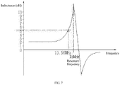
- the resonant frequency of the antenna circuit is approximate to 13.56 MHz, so as to make an inductance of the antenna circuit have a sudden change near 13.56 MHz (as shown in FIG. 7 ), to obtain a relatively high inductance.
- the NFC antenna 1 can be applied when the NFC antenna 1 approaches a high-loss environment such as metals. After the antenna circuit is affected, the inductance of the NFC antenna 1 drops to a normal level, so as to still complete wireless communication. Therefore, the NFC antenna 1 according to the embodiments of the present invention can produce a relatively high inductance with a relatively small size and thus, can complete communication when approaching a high-loss environment such as metals.
- the NFC antenna 1 includes at least one substrate 10 and at least two coils.
- the resonant frequency of the antenna circuit is 15-20 MHz.
- the two neighboring coils are connected through a via 12 in the substrate 10, a quantity of the feed points 11 is two, and the feed points 11 are respectively located at an initial end and a tail end of the antenna circuit.
- the NFC antenna 1 may be a flexible printed circuit board (FPC) or a printed circuit board (PCB) on the whole.
- the substrate 10 is a flexible board or a rigid board.
- the at least two coils may also be conductive ink or silver paste printed on the substrate 10.
- the NFC antenna according to the present invention includes a substrate 10 and two coils, that is, a first coil 20 and a second coil 30.
- the substrate 10 has a first surface and a second surface that are opposite in a thickness direction of the substrate.
- the first coil 20 is winded around an outer periphery of the first surface of the substrate 10 along a circumferential direction of the substrate 10.
- the second coil 30 is winded around an outer periphery of the second surface of the substrate 10 along a circumferential direction of the substrate 10.
- the first coil 20 and the second coil 30 are connected, and projections of the first coil 20 and the second coil 30 on the substrate 10 at least partially overlap.
- an outer end of the first coil 20 and an outer end of the second coil 30 are connected through a via 12 in the substrate 10.
- Two feed points 11 are disposed on the first surface of the substrate 10 separately, one feed point 11 is connected to an inner end of the first coil 20, the other feed point 11 is connected to an inner end of the second coil 30 through the via 12 in the substrate 10.
- the substrate 10 has a dielectric constant of 4.0 and a thickness of 30 ⁇ m, and an overlapping area of projections of the first coil 20 and the second coil 30 on the substrate 10 is 34-135 mm 2 , to ensure that a resonant frequency of an antenna circuit is 15-20 MHz.
- the NFC antenna 1 is an FPC on the whole.
- the substrate 10 has a length of 30 mm and a width of 20 mm.
- the first coil 20 and the second coil 30 both have two turns. Line widths and line distances of the first coil 20 and the second coil 3 are all 0.5 mm.
- PI polyimide
- the substrate 10 is made of polyimide (PI) and has a thickness of 30 ⁇ m, and the resonant frequency of the antenna circuit is 20 MHz.
- f is the resonant frequency of the antenna circuit
- L is an inductance of the antenna circuit
- ⁇ is the dielectric constant 4.0 of the substrate 10
- ⁇ 0 is a vacuum permittivity 8.85e-12F/m
- S is the overlapping area of the projections of the first coil 20 and the second coil 30 on the substrate 10
- d is a distance between the first coil 20 and the second coil 30 (that is, the thickness of the substrate 10).
- the NFC antenna 1 according to this embodiment of the present invention and an existing NFC antenna are separately tested by using a network analyzer.
- the existing NFC antenna whose size is 30x20 mm, quantity of turns of the coils is 4, and line widths and line distances of the coils are all 0.5 mm is used as a test object.
- a resonant frequency of the existing antenna is 85 MHz.
- the NFC antenna 1 according to this embodiment of the present invention uses a circuit of four turns to achieve an inductance of the existing NFC antenna that uses a circuit of 10 turns. Therefore, when the NFC antenna 1 according to this embodiment of the present invention and the existing NFC antenna have the same inductance, the size of the NFC antenna 1 according to this embodiment of the present invention may be reduced by 3/4 compared with the size of the existing NFC antenna.
- the NFC antenna 1 according to this embodiment of the present invention may produce a relatively high inductance with a coil of fewer turns, for example, achieve 3-6 times of the inductance of the existing NFC antenna. Therefore, after the NFC antenna 1 according to this embodiment of the present invention is affected when approaching a high-loss environment such as metals, the inductance of the NFC antenna 1 dramatically drops to a normal level, so as to still complete wireless communication.
- the substrate 10 has a dielectric constant of 4.3 and a thickness of 30 ⁇ m, and an overlapping area of projections of the first coil 20 and the second coil 30 on the substrate 10 is 32-126 mm 2 , to ensure that the resonant frequency of the antenna circuit is 15-20 MHz.
- the NFC antenna 1 is a PCB on the whole.
- the substrate 10 has a length of 30 mm and a width of 20 mm.
- the first coil 20 and the second coil 30 both have two turns. Line widths and line distances of the first coil 20 and the second coil 3 are all 0.5 mm.
- the substrate 10 is a glass-reinforced epoxy laminated sheet (FR4) and has a thickness of 30 ⁇ m, and the resonant frequency of the antenna circuit is 20 MHz.
- FR4 glass-reinforced epoxy laminated sheet
- f is the resonant frequency of the antenna circuit
- L is an inductance of the antenna circuit
- ⁇ is the dielectric constant 4.3 of the substrate 10
- ⁇ 0 is a vacuum permittivity 8.85e-12F/m
- S is the overlapping area of the projections of the first coil 20 and the second coil 30 on the substrate 10
- d is a distance between the first coil 20 and the second coil 30 (that is, the thickness of the substrate 10).
- the NFC antenna 1 according to this embodiment of the present invention and an existing NFC antenna are separately tested by using a network analyzer.
- the existing NFC antenna whose size is 30x20 mm, quantity of turns of the coils is 4, and line widths and line distances of the coils are all 0.5 mm is used as a test object.
- a resonant frequency of the existing antenna is 85 MHz.
- the NFC antenna 1 according to this embodiment of the present invention uses a circuit of four turns to achieve an inductance of the existing NFC antenna that uses a circuit of 10 turns. Therefore, when the NFC antenna 1 according to this embodiment of the present invention and the existing NFC antenna have the same inductance, the size of the NFC antenna 1 according to this embodiment of the present invention may be reduced by 3/4 compared with the size of the existing NFC antenna.
- the NFC antenna 1 according to this embodiment of the present invention may produce a relatively high inductance with a coil of fewer turns, for example, achieve 3-6 times of the inductance of the existing NFC antenna. Therefore, after the NFC antenna 1 according to this embodiment of the present invention is affected when approaching a high-loss environment such as metals, the inductance of the NFC antenna 1 dramatically drops to a normal level, so as to still complete wireless communication.
- orientation or position relationships indicated by terms “center”, “longitudinal”, “transverse”, “length”, “width”, “thickness” “on”, “under”, “front”, “rear”, “left”, “right”, “vertical”, “horizontal”, “top”, “bottom”, “inside”, “outside”, “clockwise”, “counterclockwise” or the like are orientation or position relationships shown based on the accompanying drawings, which are only for the purpose of describing the present invention and simplifying the description, but do not indicate or imply that indicated apparatuses or elements necessarily have particular orientations or are necessarily constructed and operated at particular orientations. Therefore, the orientation or position relationships should not be understood as a limitation to the present invention.
- first and second are only for descriptive purpose and cannot be understood as indicating or implying relative importance or implying a quantity of the indicated technical features. Therefore, features defining “first” and “second” can explicitly or implicitly include one or more of the features. In description of the present disclosure, “multiple” means at least two, such as two and three unless it is specifically defined otherwise.
- mount should be understood in broad sense, and for example, may be a fixed connection or a detachable connection or integration, may be a mechanical connection or an electric connection, may be a direct connection or an indirect connection by using an intermediate medium, and may be communication within two elements or an interaction relationship of two elements.
- mount should be understood in broad sense, and for example, may be a fixed connection or a detachable connection or integration, may be a mechanical connection or an electric connection, may be a direct connection or an indirect connection by using an intermediate medium, and may be communication within two elements or an interaction relationship of two elements.
- a first feature being “on” or “under” a second feature may include direct contact of the first and second features or contact of the first and second features through another feature between them rather than direct contact.
- the first feature being “on”, “above” and “up” the second feature includes the first feature being right above or diagonally above the second feature or only indicates that a horizontal height of the first feature is larger than that of the second feature.
- the first feature being “under”, “below” and “down” the second feature includes the first feature being right below or diagonally below the second feature or only indicates that a horizontal height of the first feature is smaller than that of the second feature.
- description of reference terms such as "one embodiment”, “some embodiments”, “example”, “specific example” or “some examples” means including specific features, structures, materials, or features described in the embodiment or example in at least one embodiment or example of the present invention.
- schematic expressions for the foregoing terms are not necessarily specific to the same embodiment or example.
- the described specific features, structures, materials, or features can be combined in a proper manner in any one or more embodiments or examples.
- a person skilled in the art can join or combine different embodiments or examples described in the present specification.
Landscapes
- Details Of Aerials (AREA)
Abstract
Description
- The present invention relates to the field of wireless communications, and in particular, to an NFC antenna.
- Near field communication (NFC) is short-range high-frequency wireless technology that operates within a distance of 20 cm at a frequency of 13.56 MHz. An NFC antenna in conventional technologies uses a planar coil structure and has a relatively low inductance. When an existing NFC antenna approaches a high-loss environment such as metals, an inductance of the NFC antenna dramatically drops, and as a result, communication cannot be completed.
- The present invention aims at resolving one of the foregoing technical problems in the conventional technologies to some extent. For this, the present invention provides an NFC antenna. The NFC antenna can produce a relatively high inductance with a relatively small size and can complete communication when approaching a high-loss environment such as metals.
- To achieve the foregoing objective, an NFC antenna is provided according to an embodiment of the present invention, where the NFC antenna includes: at least two coils, where the at least two coils are disposed separately and are connected in series or in parallel to form an antenna circuit; at least one substrate, where the at least two coils are disposed on the at least one substrate, and two neighboring coils of the at least two coils are spaced by a substrate of the at least one substrate, projections of the two neighboring coils on the substrate of the at least one substrate at least partially overlap, the at least one substrate is provided with feed points connected to the antenna circuit, and a resonant frequency of the antenna circuit is 15-30 MHz.
- The NFC antenna according to this embodiment of the present invention can produce a relatively high inductance with a relatively small size and can complete communication when approaching a high-loss environment such as metals.
- In addition, the NFC antenna according to this embodiment of the present invention may also have the following additional technical features:
According to an embodiment of the present invention, the resonant frequency of the antenna circuit is 15-20 MHz. - According to an embodiment of the present invention, the two neighboring coils are connected through a via in the substrate of the at least one substrate.
- According to an embodiment of the present invention, a quantity of the feed points is two, and the feed points are respectively located at an initial end and a tail end of the antenna circuit.
- According to an embodiment of the present invention, the at least one substrate is a flexible board or a rigid board.
- According to an embodiment of the present invention, the at least two coils are conductive ink or silver paste printed on the at least one substrate.
- According to an embodiment of the present invention, the NFC antenna includes: one substrate, where the substrate has a first surface and a second surface that are opposite in a thickness direction of the substrate; and a first coil and a second coil, where the first coil is disposed on the first surface, the second coil is disposed on the second surface, the first coil and the second coil are connected, and projections of the first coil and the second coil on the substrate at least partially overlap.
- According to an embodiment of the present invention, the NFC antenna further includes two feed points, where the two feed points are disposed on the first surface separately, one of the two feed points is connected to an inner end of the first coil, the other of the two feed points is connected to an inner end of the second coil, and an outer end of the first coil is connected to an outer end of the second coil.
- According to an embodiment of the present invention, the substrate has a dielectric constant of 4.0 and a thickness of 30 µm, and an overlapping area of the projections of the first coil and the second coil on the substrate is 34-135 mm2.
- According to an embodiment of the present invention, the substrate has a dielectric constant of 4.3 and a thickness of 30 µm, and an overlapping area of the projections of the first coil and the second coil on the substrate is 32-126 mm2.
-
-
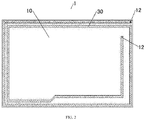
FIG. 1 is a schematic diagram of a front surface of an NFC antenna according to an embodiment of the present invention; -
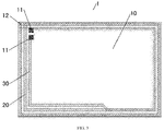
FIG. 2 is a schematic diagram of a back surface of an NFC antenna according to an embodiment of the present invention; -
FIG. 3 is a perspective view of an NFC antenna according to an embodiment of the present invention; -
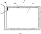
FIG. 4 is a schematic diagram of a front surface of an NFC antenna according to another embodiment of the present invention; -
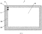
FIG. 5 is a schematic diagram of a back surface of an NFC antenna according to another embodiment of the present invention; -
FIG. 6 is a perspective view of an NFC antenna according to another embodiment of the present invention; -
FIG. 7 shows an inductance-resonance curve of an NFC antenna according to an embodiment of the present invention. - Reference numerals:
NFC antenna 1,substrate 10,feed point 11, via 12,first coil 20,second coil 30. - The following describes embodiments of the present invention in detail. Examples of the embodiments are shown in the accompanying drawings, and same or similar reference numerals throughout the specification represent same or similar elements or elements having same or similar functions. The following embodiments described with reference to the accompanying drawings are exemplary, aiming at the purpose of explaining the present invention, and should not be understood as a limitation to the present invention.
- The following describes, with reference to the accompanying drawings, an
NFC antenna 1 according to an embodiment of the present invention. - As shown in
FIG. 1 to FIG. 7 , theNFC antenna 1 according to this embodiment of the present invention includes at least onesubstrate 10 and at least two coils. - The at least two coils are disposed separately and are connected in series or in parallel to form an antenna circuit. The at least two coils are disposed on the at least one
substrate 10, and two neighboring coils of the at least two coils are spaced by a substrate of the at least onesubstrate 10, projections of the two neighboring coils of the at least two coils on the substrate of the at least one substrate at least partially overlap, the at least onesubstrate 10 is provided withfeed points 11 connected to the antenna circuit. - A person skilled in the art should understand that after different coils are stacked, when viewed from the same direction, flow directions of currents are the same, that is, the currents all flow clockwise or all flow counterclockwise. Hence, currents having a same flow direction produce magnetic fluxes having a same direction, and better performance is achieved by superposing the magnetic fluxes.
- In the
NFC antenna 1 according to this embodiment of the present invention, at least two coils are provided, and projections of the two neighboring coils of the at least two coils on the substrate of the at least onesubstrate 10 at least partially overlap. In this way, a capacitance is increased by adjusting an overlapping area of projections of the two neighboring coils on thesubstrate 10, so as to reduce a resonant frequency of the antenna circuit. Thus, the resonant frequency of the antenna circuit is approximate to 13.56 MHz, so as to make an inductance of the antenna circuit have a sudden change near 13.56 MHz (as shown inFIG. 7 ), to obtain a relatively high inductance. Hence, theNFC antenna 1 can be applied when theNFC antenna 1 approaches a high-loss environment such as metals. After the antenna circuit is affected, the inductance of theNFC antenna 1 drops to a normal level, so as to still complete wireless communication. Therefore, theNFC antenna 1 according to the embodiments of the present invention can produce a relatively high inductance with a relatively small size and thus, can complete communication when approaching a high-loss environment such as metals. - The following describes, with reference to the accompanying drawings, the
NFC antenna 1 according to specific embodiments of the present invention. - In some specific embodiments of the present invention, as shown in
FIG. 1 to FIG. 7 , theNFC antenna 1 according to this embodiment of the present invention includes at least onesubstrate 10 and at least two coils. - To ensure that the inductance of the antenna circuit has a sudden change near 13.56 MHz, an overlapping area of projections of two neighboring coils on the
substrate 10 is adjusted according to a formula f=1/[2π√(LC)] and C=ε*ε0*S/d, so that the resonant frequency of the antenna circuit is 15-30 MHz. Preferably, the resonant frequency of the antenna circuit is 15-20 MHz. - Specifically, the two neighboring coils are connected through a
via 12 in thesubstrate 10, a quantity of thefeed points 11 is two, and thefeed points 11 are respectively located at an initial end and a tail end of the antenna circuit. - Optionally, the
NFC antenna 1 may be a flexible printed circuit board (FPC) or a printed circuit board (PCB) on the whole. In other words, thesubstrate 10 is a flexible board or a rigid board. - Certainly, the present invention is not limited thereto. The at least two coils may also be conductive ink or silver paste printed on the
substrate 10. - In some specific embodiments of the present invention, as shown in
FIG. 1 to FIG. 6 , the NFC antenna according to the present invention includes asubstrate 10 and two coils, that is, afirst coil 20 and asecond coil 30. Thesubstrate 10 has a first surface and a second surface that are opposite in a thickness direction of the substrate. Thefirst coil 20 is winded around an outer periphery of the first surface of thesubstrate 10 along a circumferential direction of thesubstrate 10. Thesecond coil 30 is winded around an outer periphery of the second surface of thesubstrate 10 along a circumferential direction of thesubstrate 10. Thefirst coil 20 and thesecond coil 30 are connected, and projections of thefirst coil 20 and thesecond coil 30 on thesubstrate 10 at least partially overlap. - Specifically, an outer end of the
first coil 20 and an outer end of thesecond coil 30 are connected through avia 12 in thesubstrate 10. Twofeed points 11 are disposed on the first surface of thesubstrate 10 separately, onefeed point 11 is connected to an inner end of thefirst coil 20, theother feed point 11 is connected to an inner end of thesecond coil 30 through thevia 12 in thesubstrate 10. - In some specific examples of the present invention, as shown in
FIG. 1 to FIG. 3 , thesubstrate 10 has a dielectric constant of 4.0 and a thickness of 30 µm, and an overlapping area of projections of thefirst coil 20 and thesecond coil 30 on thesubstrate 10 is 34-135 mm2, to ensure that a resonant frequency of an antenna circuit is 15-20 MHz. - For example, the
NFC antenna 1 is an FPC on the whole. Thesubstrate 10 has a length of 30 mm and a width of 20 mm. Thefirst coil 20 and thesecond coil 30 both have two turns. Line widths and line distances of thefirst coil 20 and the second coil 3 are all 0.5 mm. Hence, a person skilled in the art can calculate inductance values of the coils according to the prior art. In addition, thesubstrate 10 is made of polyimide (PI) and has a thickness of 30 µm, and the resonant frequency of the antenna circuit is 20 MHz. - Further, C=90 picofarads may be obtained according to a formula f=1/[2π√(LC)]. Ignoring a capacitance between parallel lines, to make a planar capacitance between different layers be 90 picofarads, an S value of 76 mm2 when a capacitance is 90 picofarads is obtained by calculation according to C=ε*ε0*S/d. Therefore, the overlapping area of the projections of the
first coil 20 and thesecond coil 30 on thesubstrate 10 is adjusted to 76 mm2. - Here, f is the resonant frequency of the antenna circuit, L is an inductance of the antenna circuit, ε is the dielectric constant 4.0 of the
substrate 10, ε0 is a vacuum permittivity 8.85e-12F/m, S is the overlapping area of the projections of thefirst coil 20 and thesecond coil 30 on thesubstrate 10, and d is a distance between thefirst coil 20 and the second coil 30 (that is, the thickness of the substrate 10). - The
NFC antenna 1 according to this embodiment of the present invention and an existing NFC antenna are separately tested by using a network analyzer. The existing NFC antenna whose size is 30x20 mm, quantity of turns of the coils is 4, and line widths and line distances of the coils are all 0.5 mm is used as a test object. A resonant frequency of the existing antenna is 85 MHz. - It is obtained by testing that an inductance of the existing NFC antenna at 13.56 MHz is 0.8 microhenry, and an inductance of the
NFC antenna 1 according to this embodiment of the present invention at 13.56 MHz is 2.3 microhenries. - By comparing the test results, the
NFC antenna 1 according to this embodiment of the present invention uses a circuit of four turns to achieve an inductance of the existing NFC antenna that uses a circuit of 10 turns. Therefore, when theNFC antenna 1 according to this embodiment of the present invention and the existing NFC antenna have the same inductance, the size of theNFC antenna 1 according to this embodiment of the present invention may be reduced by 3/4 compared with the size of the existing NFC antenna. In addition, when approaching a high-loss environment such as metals, theNFC antenna 1 according to this embodiment of the present invention may produce a relatively high inductance with a coil of fewer turns, for example, achieve 3-6 times of the inductance of the existing NFC antenna. Therefore, after theNFC antenna 1 according to this embodiment of the present invention is affected when approaching a high-loss environment such as metals, the inductance of theNFC antenna 1 dramatically drops to a normal level, so as to still complete wireless communication. - In some other specific examples of the present invention, as shown in
FIG. 4 to FIG. 6 , thesubstrate 10 has a dielectric constant of 4.3 and a thickness of 30 µm, and an overlapping area of projections of thefirst coil 20 and thesecond coil 30 on thesubstrate 10 is 32-126 mm2, to ensure that the resonant frequency of the antenna circuit is 15-20 MHz. - For example, the
NFC antenna 1 is a PCB on the whole. Thesubstrate 10 has a length of 30 mm and a width of 20 mm. Thefirst coil 20 and thesecond coil 30 both have two turns. Line widths and line distances of thefirst coil 20 and the second coil 3 are all 0.5 mm. Hence, a person skilled in the art can calculate inductance values of the coils according to the prior art. In addition, thesubstrate 10 is a glass-reinforced epoxy laminated sheet (FR4) and has a thickness of 30 µm, and the resonant frequency of the antenna circuit is 20 MHz. - Further, C=90 picofarads may be obtained according to a formula f=1/[2π√(LC)]. Ignoring a capacitance between parallel lines, to make a planar capacitance between different layers be 90 picofarads, an S value of 71 mm2 when a capacitance is 90 picofarads is obtained by calculation according to C=ε*ε0*S/d. Therefore, the overlapping area of the projections of the
first coil 20 and thesecond coil 30 on thesubstrate 10 is adjusted to 71 mm2. - Here, f is the resonant frequency of the antenna circuit, L is an inductance of the antenna circuit, ε is the dielectric constant 4.3 of the
substrate 10, ε0 is a vacuum permittivity 8.85e-12F/m, S is the overlapping area of the projections of thefirst coil 20 and thesecond coil 30 on thesubstrate 10, and d is a distance between thefirst coil 20 and the second coil 30 (that is, the thickness of the substrate 10). - The
NFC antenna 1 according to this embodiment of the present invention and an existing NFC antenna are separately tested by using a network analyzer. The existing NFC antenna whose size is 30x20 mm, quantity of turns of the coils is 4, and line widths and line distances of the coils are all 0.5 mm is used as a test object. A resonant frequency of the existing antenna is 85 MHz. - It is obtained by testing that an inductance of the existing NFC antenna at 13.56 MHz is 0.8 microhenry, and an inductance of the
NFC antenna 1 according to this embodiment of the present invention at 13.56 MHz is 2.4 microhenries. - By comparing the test results, the
NFC antenna 1 according to this embodiment of the present invention uses a circuit of four turns to achieve an inductance of the existing NFC antenna that uses a circuit of 10 turns. Therefore, when theNFC antenna 1 according to this embodiment of the present invention and the existing NFC antenna have the same inductance, the size of theNFC antenna 1 according to this embodiment of the present invention may be reduced by 3/4 compared with the size of the existing NFC antenna. In addition, when approaching a high-loss environment such as metals, theNFC antenna 1 according to this embodiment of the present invention may produce a relatively high inductance with a coil of fewer turns, for example, achieve 3-6 times of the inductance of the existing NFC antenna. Therefore, after theNFC antenna 1 according to this embodiment of the present invention is affected when approaching a high-loss environment such as metals, the inductance of theNFC antenna 1 dramatically drops to a normal level, so as to still complete wireless communication. - Other structures and operations of the
NFC antenna 1 according to the embodiments of the present invention are known to a person of ordinary skill in the art and are not described in detail herein. - In description of the present invention, it should be understood that orientation or position relationships indicated by terms "center", "longitudinal", "transverse", "length", "width", "thickness" "on", "under", "front", "rear", "left", "right", "vertical", "horizontal", "top", "bottom", "inside", "outside", "clockwise", "counterclockwise" or the like are orientation or position relationships shown based on the accompanying drawings, which are only for the purpose of describing the present invention and simplifying the description, but do not indicate or imply that indicated apparatuses or elements necessarily have particular orientations or are necessarily constructed and operated at particular orientations. Therefore, the orientation or position relationships should not be understood as a limitation to the present invention.
- In addition, terms "first" and "second" are only for descriptive purpose and cannot be understood as indicating or implying relative importance or implying a quantity of the indicated technical features. Therefore, features defining "first" and "second" can explicitly or implicitly include one or more of the features. In description of the present disclosure, "multiple" means at least two, such as two and three unless it is specifically defined otherwise.
- In the present invention, unless explicitly stipulated and defined otherwise, terms such as "mount", "link", "connect", and "fasten" should be understood in broad sense, and for example, may be a fixed connection or a detachable connection or integration, may be a mechanical connection or an electric connection, may be a direct connection or an indirect connection by using an intermediate medium, and may be communication within two elements or an interaction relationship of two elements. A person of ordinary skill in the art could understand specific meanings of the terms in the present invention according to specific situations.
- In the present invention, unless explicitly stipulated and defined otherwise, a first feature being "on" or "under" a second feature may include direct contact of the first and second features or contact of the first and second features through another feature between them rather than direct contact. In addition, the first feature being "on", "above" and "up" the second feature includes the first feature being right above or diagonally above the second feature or only indicates that a horizontal height of the first feature is larger than that of the second feature. In addition, the first feature being "under", "below" and "down" the second feature includes the first feature being right below or diagonally below the second feature or only indicates that a horizontal height of the first feature is smaller than that of the second feature.
- In description of the present specification, description of reference terms such as "one embodiment", "some embodiments", "example", "specific example" or "some examples" means including specific features, structures, materials, or features described in the embodiment or example in at least one embodiment or example of the present invention. In the present specification, schematic expressions for the foregoing terms are not necessarily specific to the same embodiment or example. In addition, the described specific features, structures, materials, or features can be combined in a proper manner in any one or more embodiments or examples. In addition, a person skilled in the art can join or combine different embodiments or examples described in the present specification.
- Although the embodiments of the present invention are shown and described in the above, it can be understood that the foregoing embodiments are exemplary and cannot be understood as a limitation to the present invention. A person of ordinary skill in the art can change, modify, replace, and deform the foregoing embodiments within the scope of the present invention.
Claims (10)
- An NFC antenna, comprising:at least two coils, wherein the at least two coils are disposed separately and are connected in series or in parallel to form an antenna circuit;at least one substrate, wherein the at least two coils are disposed on the at least one substrate, and two neighboring coils of the at least two coils are spaced by a substrate of the at least one substrate, projections of the two neighboring coils on the substrate of the at least one substrate at least partially overlap, the at least one substrate is provided with feed points connected to the antenna circuit, and a resonant frequency of the antenna circuit is 15-30 MHz.
- The NFC antenna according to claim 1, wherein the resonant frequency of the antenna circuit is 15-20 MHz.
- The NFC antenna according to claim 1 or 2, wherein the two neighboring coils are connected through a via in the substrate of the at least one substrate.
- The NFC antenna according to any one of claims 1 to 3, wherein a quantity of the feed points is two, and the feed points are respectively located at an initial end and a tail end of the antenna circuit.
- The NFC antenna according to any one of claims 1 to 4, wherein the at least one substrate is a flexible board or a rigid board.
- The NFC antenna according to any one of claims 1 to 5, wherein the at least two coils are conductive ink or silver paste printed on the at least one substrate.
- The NFC antenna according to any one of claims 1 to 6, comprising:one substrate, wherein the substrate has a first surface and a second surface that are opposite in a thickness direction of the substrate; anda first coil and a second coil, wherein the first coil is disposed on the first surface, the second coil is disposed on the second surface, the first coil and the second coil are connected, and projections of the first coil and the second coil on the substrate at least partially overlap.
- The NFC antenna according to claim 7, further comprising two feed points, wherein the two feed points are disposed on the first surface separately, one of the two feed points is connected to an inner end of the first coil, the other of the two feed points is connected to an inner end of the second coil, and an outer end of the first coil is connected to an outer end of the second coil.
- The NFC antenna according to claim 7 or 8, wherein the substrate has a dielectric constant of 4.0 and a thickness of 30 µm, and an overlapping area of the projections of the first coil and the second coil on the substrate is 34-135 mm2.
- The NFC antenna according to claim 7 or 8, wherein the substrate has a dielectric constant of 4.3 and a thickness of 30 µm, and an area of an overlapped part of the projections of the first coil and the second coil on the substrate is 32-126 mm2.
Applications Claiming Priority (2)
| Application Number | Priority Date | Filing Date | Title |
|---|---|---|---|
| CN201510390035.5A CN106329096B (en) | 2015-06-30 | 2015-06-30 | NFC antenna |
| PCT/CN2016/085722 WO2017000769A1 (en) | 2015-06-30 | 2016-06-14 | Nfc antenna |
Publications (2)
| Publication Number | Publication Date |
|---|---|
| EP3319173A1 true EP3319173A1 (en) | 2018-05-09 |
| EP3319173A4 EP3319173A4 (en) | 2019-02-13 |
Family
ID=57607872
Family Applications (1)
| Application Number | Title | Priority Date | Filing Date |
|---|---|---|---|
| EP16817133.8A Withdrawn EP3319173A4 (en) | 2015-06-30 | 2016-06-14 | Nfc antenna |
Country Status (4)
| Country | Link |
|---|---|
| US (1) | US20180191069A1 (en) |
| EP (1) | EP3319173A4 (en) |
| CN (1) | CN106329096B (en) |
| WO (1) | WO2017000769A1 (en) |
Cited By (1)
| Publication number | Priority date | Publication date | Assignee | Title |
|---|---|---|---|---|
| CN111508340A (en) * | 2020-04-26 | 2020-08-07 | 厦门天马微电子有限公司 | Display module, preparation method and display device |
Families Citing this family (9)
| Publication number | Priority date | Publication date | Assignee | Title |
|---|---|---|---|---|
| EP3071288B1 (en) | 2013-11-19 | 2018-11-14 | The Cleveland Clinic Foundation | System for treating obstructive sleep apnea using a neuromuscular stimulator |
| US11771899B2 (en) | 2018-07-10 | 2023-10-03 | The Cleveland Clinic Foundation | System and method for treating obstructive sleep apnea |
| WO2020223740A1 (en) | 2019-05-02 | 2020-11-05 | Enhale Medical, Inc. | Systems and methods for improving sleep disordered breathing |
| US11351377B2 (en) | 2019-05-03 | 2022-06-07 | The Cleveland Clinic Foundation | Intra-oral appliances and systems |
| WO2021076188A1 (en) | 2019-10-15 | 2021-04-22 | Enhale Medical, Inc. | Biased neuromodulation lead and method of using same |
| US11691010B2 (en) | 2021-01-13 | 2023-07-04 | Xii Medical, Inc. | Systems and methods for improving sleep disordered breathing |
| CN114361812B (en) * | 2021-12-28 | 2025-10-31 | 歌尔科技有限公司 | NFC antenna assembly, manufacturing method and electronic equipment |
| CN114204251A (en) * | 2021-12-31 | 2022-03-18 | 深圳市卓睿通信技术有限公司 | NFC antenna with conductive back adhesive and terminal |
| CN114709613A (en) * | 2022-04-25 | 2022-07-05 | 深圳市卓睿通信技术有限公司 | NFC antenna and terminal with low blind area reading function |
Family Cites Families (13)
| Publication number | Priority date | Publication date | Assignee | Title |
|---|---|---|---|---|
| US4689636A (en) * | 1985-03-15 | 1987-08-25 | Minnesota Mining And Manufacturing Company | Deactivatable resonant marker for use in RF electronic article surveillance system |
| WO2005093900A1 (en) * | 2004-03-26 | 2005-10-06 | Semiconductor Energy Laboratory Co., Ltd. | Semiconductor device |
| CN2888666Y (en) * | 2005-11-14 | 2007-04-11 | 北京握奇数据系统有限公司 | Antenna assembly for plug-in intelligent card non-contact interface |
| WO2010066955A1 (en) * | 2008-12-11 | 2010-06-17 | Yves Eray | Rfid antenna circuit |
| DE102009004130A1 (en) * | 2009-01-05 | 2010-07-08 | Leonhard Kurz Stiftung & Co. Kg | Multilayer film element |
| CN105514589B (en) * | 2010-06-18 | 2018-11-23 | 株式会社村田制作所 | Communication terminal device |
| CN103053073B (en) * | 2010-07-29 | 2016-05-25 | 株式会社村田制作所 | Resonant circuit and antenna device |
| CN202009072U (en) * | 2011-02-25 | 2011-10-12 | 比亚迪股份有限公司 | Near field communication antenna |
| CN102608662B (en) * | 2012-03-23 | 2015-04-01 | 刘冀成 | Detection device based on transient electromagnetic method (TEM) |
| CN102646866A (en) * | 2012-04-17 | 2012-08-22 | 中兴通讯股份有限公司 | Near field communication (NFC) antenna and terminal equipment |
| WO2013183552A1 (en) * | 2012-06-04 | 2013-12-12 | 株式会社村田製作所 | Antenna device and communication terminal device |
| WO2013183575A1 (en) * | 2012-06-04 | 2013-12-12 | 株式会社村田製作所 | Antenna apparatus and wireless communication apparatus |
| DE102013102051A1 (en) * | 2013-03-01 | 2014-09-04 | Infineon Technologies Ag | Booster antenna, contactless chip arrangement, antenna structure, and chip arrangement |
-
2015
- 2015-06-30 CN CN201510390035.5A patent/CN106329096B/en active Active
-
2016
- 2016-06-14 US US15/739,196 patent/US20180191069A1/en not_active Abandoned
- 2016-06-14 EP EP16817133.8A patent/EP3319173A4/en not_active Withdrawn
- 2016-06-14 WO PCT/CN2016/085722 patent/WO2017000769A1/en not_active Ceased
Cited By (1)
| Publication number | Priority date | Publication date | Assignee | Title |
|---|---|---|---|---|
| CN111508340A (en) * | 2020-04-26 | 2020-08-07 | 厦门天马微电子有限公司 | Display module, preparation method and display device |
Also Published As
| Publication number | Publication date |
|---|---|
| WO2017000769A1 (en) | 2017-01-05 |
| US20180191069A1 (en) | 2018-07-05 |
| EP3319173A4 (en) | 2019-02-13 |
| CN106329096A (en) | 2017-01-11 |
| CN106329096B (en) | 2020-03-31 |
Similar Documents
| Publication | Publication Date | Title |
|---|---|---|
| US20180191069A1 (en) | Nfc antenna | |
| US9088069B2 (en) | Wireless communication apparatus | |
| US8400231B2 (en) | High-frequency coupler and communication device | |
| JP6465109B2 (en) | Multi-antenna and radio apparatus including the same | |
| CN102341957B (en) | Antenna device and communication terminal apparatus | |
| US9298873B2 (en) | Method of designing impedance transformation circuit | |
| US20120139814A1 (en) | Frequency stabilization circuit, antenna device, and communication terminal device | |
| US10170836B2 (en) | Coil antenna device and antenna module | |
| JP6796429B2 (en) | Antenna system and antenna module that reduces interference between radiation patterns | |
| US8952850B2 (en) | Mimo antenna apparatus | |
| US10340877B2 (en) | Antenna matching circuit, antenna device, and communication terminal apparatus | |
| JP6528496B2 (en) | Antenna device | |
| JP6269902B2 (en) | ANTENNA DEVICE AND ELECTRONIC DEVICE | |
| CN102044738A (en) | Metamaterial antenna with mechanical connection | |
| JP6288105B2 (en) | Transformer and communication terminal device | |
| JP5994500B2 (en) | Coupling degree adjusting element, antenna device, and wireless communication device | |
| US20190008042A1 (en) | Multilayer substrate | |
| US20170149136A1 (en) | Eight-frequency band antenna | |
| JP6762886B2 (en) | Antenna and antenna module | |
| US20240356209A1 (en) | Devices with Radiating Systems Proximate to Conductive Bodies | |
| JP2012147119A (en) | Electromagnetic coupler, and information communication device having the same | |
| CN102709685A (en) | A PCB five-band antenna | |
| CN102798872B (en) | Navigation device | |
| CN115708259A (en) | Antenna assembly and electronic equipment | |
| CN206293613U (en) | A kind of small size PCB printed board radio-frequency antennas for 433MHz RF communication systems |
Legal Events
| Date | Code | Title | Description |
|---|---|---|---|
| PUAI | Public reference made under article 153(3) epc to a published international application that has entered the european phase |
Free format text: ORIGINAL CODE: 0009012 |
|
| 17P | Request for examination filed |
Effective date: 20180122 |
|
| AK | Designated contracting states |
Kind code of ref document: A1 Designated state(s): AL AT BE BG CH CY CZ DE DK EE ES FI FR GB GR HR HU IE IS IT LI LT LU LV MC MK MT NL NO PL PT RO RS SE SI SK SM TR |
|
| AX | Request for extension of the european patent |
Extension state: BA ME |
|
| DAV | Request for validation of the european patent (deleted) | ||
| DAX | Request for extension of the european patent (deleted) | ||
| A4 | Supplementary search report drawn up and despatched |
Effective date: 20190116 |
|
| RIC1 | Information provided on ipc code assigned before grant |
Ipc: H01Q 7/00 20060101AFI20190110BHEP Ipc: H01Q 1/22 20060101ALI20190110BHEP Ipc: H01Q 1/38 20060101ALI20190110BHEP |
|
| STAA | Information on the status of an ep patent application or granted ep patent |
Free format text: STATUS: THE APPLICATION HAS BEEN WITHDRAWN |
|
| 18W | Application withdrawn |
Effective date: 20190930 |