EP3319127A1 - Field effect transistor device with separate source and body contacts and method of producing the device - Google Patents
Field effect transistor device with separate source and body contacts and method of producing the device Download PDFInfo
- Publication number
- EP3319127A1 EP3319127A1 EP16197521.4A EP16197521A EP3319127A1 EP 3319127 A1 EP3319127 A1 EP 3319127A1 EP 16197521 A EP16197521 A EP 16197521A EP 3319127 A1 EP3319127 A1 EP 3319127A1
- Authority
- EP
- European Patent Office
- Prior art keywords
- source
- gate electrode
- region
- electrode layer
- electric conductivity
- Prior art date
- Legal status (The legal status is an assumption and is not a legal conclusion. Google has not performed a legal analysis and makes no representation as to the accuracy of the status listed.)
- Granted
Links
Images



Classifications
-
- H—ELECTRICITY
- H10—SEMICONDUCTOR DEVICES; ELECTRIC SOLID-STATE DEVICES NOT OTHERWISE PROVIDED FOR
- H10D—INORGANIC ELECTRIC SEMICONDUCTOR DEVICES
- H10D30/00—Field-effect transistors [FET]
- H10D30/60—Insulated-gate field-effect transistors [IGFET]
- H10D30/601—Insulated-gate field-effect transistors [IGFET] having lightly-doped drain or source extensions, e.g. LDD IGFETs or DDD IGFETs
-
- H—ELECTRICITY
- H10—SEMICONDUCTOR DEVICES; ELECTRIC SOLID-STATE DEVICES NOT OTHERWISE PROVIDED FOR
- H10D—INORGANIC ELECTRIC SEMICONDUCTOR DEVICES
- H10D30/00—Field-effect transistors [FET]
- H10D30/01—Manufacture or treatment
- H10D30/021—Manufacture or treatment of FETs having insulated gates [IGFET]
- H10D30/022—Manufacture or treatment of FETs having insulated gates [IGFET] having lightly-doped source or drain extensions selectively formed at the sides of the gates
-
- H—ELECTRICITY
- H10—SEMICONDUCTOR DEVICES; ELECTRIC SOLID-STATE DEVICES NOT OTHERWISE PROVIDED FOR
- H10D—INORGANIC ELECTRIC SEMICONDUCTOR DEVICES
- H10D30/00—Field-effect transistors [FET]
- H10D30/01—Manufacture or treatment
- H10D30/021—Manufacture or treatment of FETs having insulated gates [IGFET]
- H10D30/028—Manufacture or treatment of FETs having insulated gates [IGFET] of double-diffused metal oxide semiconductor [DMOS] FETs
-
- H—ELECTRICITY
- H10—SEMICONDUCTOR DEVICES; ELECTRIC SOLID-STATE DEVICES NOT OTHERWISE PROVIDED FOR
- H10D—INORGANIC ELECTRIC SEMICONDUCTOR DEVICES
- H10D30/00—Field-effect transistors [FET]
- H10D30/01—Manufacture or treatment
- H10D30/021—Manufacture or treatment of FETs having insulated gates [IGFET]
- H10D30/028—Manufacture or treatment of FETs having insulated gates [IGFET] of double-diffused metal oxide semiconductor [DMOS] FETs
- H10D30/0281—Manufacture or treatment of FETs having insulated gates [IGFET] of double-diffused metal oxide semiconductor [DMOS] FETs of lateral DMOS [LDMOS] FETs
-
- H—ELECTRICITY
- H10—SEMICONDUCTOR DEVICES; ELECTRIC SOLID-STATE DEVICES NOT OTHERWISE PROVIDED FOR
- H10D—INORGANIC ELECTRIC SEMICONDUCTOR DEVICES
- H10D30/00—Field-effect transistors [FET]
- H10D30/60—Insulated-gate field-effect transistors [IGFET]
- H10D30/64—Double-diffused metal-oxide semiconductor [DMOS] FETs
-
- H—ELECTRICITY
- H10—SEMICONDUCTOR DEVICES; ELECTRIC SOLID-STATE DEVICES NOT OTHERWISE PROVIDED FOR
- H10D—INORGANIC ELECTRIC SEMICONDUCTOR DEVICES
- H10D30/00—Field-effect transistors [FET]
- H10D30/60—Insulated-gate field-effect transistors [IGFET]
- H10D30/64—Double-diffused metal-oxide semiconductor [DMOS] FETs
- H10D30/65—Lateral DMOS [LDMOS] FETs
-
- H—ELECTRICITY
- H10—SEMICONDUCTOR DEVICES; ELECTRIC SOLID-STATE DEVICES NOT OTHERWISE PROVIDED FOR
- H10D—INORGANIC ELECTRIC SEMICONDUCTOR DEVICES
- H10D62/00—Semiconductor bodies, or regions thereof, of devices having potential barriers
- H10D62/10—Shapes, relative sizes or dispositions of the regions of the semiconductor bodies; Shapes of the semiconductor bodies
- H10D62/124—Shapes, relative sizes or dispositions of the regions of semiconductor bodies or of junctions between the regions
- H10D62/126—Top-view geometrical layouts of the regions or the junctions
-
- H—ELECTRICITY
- H10—SEMICONDUCTOR DEVICES; ELECTRIC SOLID-STATE DEVICES NOT OTHERWISE PROVIDED FOR
- H10D—INORGANIC ELECTRIC SEMICONDUCTOR DEVICES
- H10D62/00—Semiconductor bodies, or regions thereof, of devices having potential barriers
- H10D62/10—Shapes, relative sizes or dispositions of the regions of the semiconductor bodies; Shapes of the semiconductor bodies
- H10D62/124—Shapes, relative sizes or dispositions of the regions of semiconductor bodies or of junctions between the regions
- H10D62/126—Top-view geometrical layouts of the regions or the junctions
- H10D62/127—Top-view geometrical layouts of the regions or the junctions of cellular field-effect devices, e.g. multicellular DMOS transistors or IGBTs
-
- H—ELECTRICITY
- H10—SEMICONDUCTOR DEVICES; ELECTRIC SOLID-STATE DEVICES NOT OTHERWISE PROVIDED FOR
- H10D—INORGANIC ELECTRIC SEMICONDUCTOR DEVICES
- H10D62/00—Semiconductor bodies, or regions thereof, of devices having potential barriers
- H10D62/10—Shapes, relative sizes or dispositions of the regions of the semiconductor bodies; Shapes of the semiconductor bodies
- H10D62/13—Semiconductor regions connected to electrodes carrying current to be rectified, amplified or switched, e.g. source or drain regions
- H10D62/149—Source or drain regions of field-effect devices
- H10D62/151—Source or drain regions of field-effect devices of IGFETs
- H10D62/152—Source regions of DMOS transistors
-
- H—ELECTRICITY
- H10—SEMICONDUCTOR DEVICES; ELECTRIC SOLID-STATE DEVICES NOT OTHERWISE PROVIDED FOR
- H10D—INORGANIC ELECTRIC SEMICONDUCTOR DEVICES
- H10D62/00—Semiconductor bodies, or regions thereof, of devices having potential barriers
- H10D62/10—Shapes, relative sizes or dispositions of the regions of the semiconductor bodies; Shapes of the semiconductor bodies
- H10D62/13—Semiconductor regions connected to electrodes carrying current to be rectified, amplified or switched, e.g. source or drain regions
- H10D62/149—Source or drain regions of field-effect devices
- H10D62/151—Source or drain regions of field-effect devices of IGFETs
- H10D62/152—Source regions of DMOS transistors
- H10D62/154—Dispositions
-
- H—ELECTRICITY
- H10—SEMICONDUCTOR DEVICES; ELECTRIC SOLID-STATE DEVICES NOT OTHERWISE PROVIDED FOR
- H10D—INORGANIC ELECTRIC SEMICONDUCTOR DEVICES
- H10D62/00—Semiconductor bodies, or regions thereof, of devices having potential barriers
- H10D62/10—Shapes, relative sizes or dispositions of the regions of the semiconductor bodies; Shapes of the semiconductor bodies
- H10D62/13—Semiconductor regions connected to electrodes carrying current to be rectified, amplified or switched, e.g. source or drain regions
- H10D62/149—Source or drain regions of field-effect devices
- H10D62/151—Source or drain regions of field-effect devices of IGFETs
- H10D62/152—Source regions of DMOS transistors
- H10D62/155—Shapes
-
- H—ELECTRICITY
- H10—SEMICONDUCTOR DEVICES; ELECTRIC SOLID-STATE DEVICES NOT OTHERWISE PROVIDED FOR
- H10D—INORGANIC ELECTRIC SEMICONDUCTOR DEVICES
- H10D62/00—Semiconductor bodies, or regions thereof, of devices having potential barriers
- H10D62/10—Shapes, relative sizes or dispositions of the regions of the semiconductor bodies; Shapes of the semiconductor bodies
- H10D62/17—Semiconductor regions connected to electrodes not carrying current to be rectified, amplified or switched, e.g. channel regions
- H10D62/213—Channel regions of field-effect devices
- H10D62/221—Channel regions of field-effect devices of FETs
- H10D62/235—Channel regions of field-effect devices of FETs of IGFETs
- H10D62/299—Channel regions of field-effect devices of FETs of IGFETs having lateral doping variations
-
- H—ELECTRICITY
- H10—SEMICONDUCTOR DEVICES; ELECTRIC SOLID-STATE DEVICES NOT OTHERWISE PROVIDED FOR
- H10D—INORGANIC ELECTRIC SEMICONDUCTOR DEVICES
- H10D62/00—Semiconductor bodies, or regions thereof, of devices having potential barriers
- H10D62/10—Shapes, relative sizes or dispositions of the regions of the semiconductor bodies; Shapes of the semiconductor bodies
- H10D62/17—Semiconductor regions connected to electrodes not carrying current to be rectified, amplified or switched, e.g. channel regions
- H10D62/393—Body regions of DMOS transistors or IGBTs
-
- H—ELECTRICITY
- H10—SEMICONDUCTOR DEVICES; ELECTRIC SOLID-STATE DEVICES NOT OTHERWISE PROVIDED FOR
- H10D—INORGANIC ELECTRIC SEMICONDUCTOR DEVICES
- H10D64/00—Electrodes of devices having potential barriers
- H10D64/01—Manufacture or treatment
- H10D64/011—Manufacture or treatment of electrodes ohmically coupled to a semiconductor
- H10D64/0111—Manufacture or treatment of electrodes ohmically coupled to a semiconductor to Group IV semiconductors
- H10D64/0115—Manufacture or treatment of electrodes ohmically coupled to a semiconductor to Group IV semiconductors to silicon carbide
-
- H—ELECTRICITY
- H10—SEMICONDUCTOR DEVICES; ELECTRIC SOLID-STATE DEVICES NOT OTHERWISE PROVIDED FOR
- H10D—INORGANIC ELECTRIC SEMICONDUCTOR DEVICES
- H10D64/00—Electrodes of devices having potential barriers
- H10D64/20—Electrodes characterised by their shapes, relative sizes or dispositions
- H10D64/27—Electrodes not carrying the current to be rectified, amplified, oscillated or switched, e.g. gates
- H10D64/311—Gate electrodes for field-effect devices
- H10D64/411—Gate electrodes for field-effect devices for FETs
- H10D64/511—Gate electrodes for field-effect devices for FETs for IGFETs
- H10D64/517—Gate electrodes for field-effect devices for FETs for IGFETs characterised by the conducting layers
- H10D64/519—Gate electrodes for field-effect devices for FETs for IGFETs characterised by the conducting layers characterised by their top-view geometrical layouts
-
- H—ELECTRICITY
- H10—SEMICONDUCTOR DEVICES; ELECTRIC SOLID-STATE DEVICES NOT OTHERWISE PROVIDED FOR
- H10P—GENERIC PROCESSES OR APPARATUS FOR THE MANUFACTURE OR TREATMENT OF DEVICES COVERED BY CLASS H10
- H10P30/00—Ion implantation into wafers, substrates or parts of devices
- H10P30/20—Ion implantation into wafers, substrates or parts of devices into semiconductor materials, e.g. for doping
- H10P30/202—Ion implantation into wafers, substrates or parts of devices into semiconductor materials, e.g. for doping characterised by the semiconductor materials
- H10P30/204—Ion implantation into wafers, substrates or parts of devices into semiconductor materials, e.g. for doping characterised by the semiconductor materials into Group IV semiconductors
-
- H—ELECTRICITY
- H10—SEMICONDUCTOR DEVICES; ELECTRIC SOLID-STATE DEVICES NOT OTHERWISE PROVIDED FOR
- H10P—GENERIC PROCESSES OR APPARATUS FOR THE MANUFACTURE OR TREATMENT OF DEVICES COVERED BY CLASS H10
- H10P30/00—Ion implantation into wafers, substrates or parts of devices
- H10P30/20—Ion implantation into wafers, substrates or parts of devices into semiconductor materials, e.g. for doping
- H10P30/21—Ion implantation into wafers, substrates or parts of devices into semiconductor materials, e.g. for doping of electrically active species
-
- H—ELECTRICITY
- H10—SEMICONDUCTOR DEVICES; ELECTRIC SOLID-STATE DEVICES NOT OTHERWISE PROVIDED FOR
- H10W—GENERIC PACKAGES, INTERCONNECTIONS, CONNECTORS OR OTHER CONSTRUCTIONAL DETAILS OF DEVICES COVERED BY CLASS H10
- H10W20/00—Interconnections in chips, wafers or substrates
- H10W20/20—Interconnections within wafers or substrates, e.g. through-silicon vias [TSV]
-
- H—ELECTRICITY
- H10—SEMICONDUCTOR DEVICES; ELECTRIC SOLID-STATE DEVICES NOT OTHERWISE PROVIDED FOR
- H10W—GENERIC PACKAGES, INTERCONNECTIONS, CONNECTORS OR OTHER CONSTRUCTIONAL DETAILS OF DEVICES COVERED BY CLASS H10
- H10W20/00—Interconnections in chips, wafers or substrates
- H10W20/40—Interconnections external to wafers or substrates, e.g. back-end-of-line [BEOL] metallisations or vias connecting to gate electrodes
- H10W20/41—Interconnections external to wafers or substrates, e.g. back-end-of-line [BEOL] metallisations or vias connecting to gate electrodes characterised by their conductive parts
- H10W20/42—Vias, e.g. via plugs
-
- H—ELECTRICITY
- H10—SEMICONDUCTOR DEVICES; ELECTRIC SOLID-STATE DEVICES NOT OTHERWISE PROVIDED FOR
- H10D—INORGANIC ELECTRIC SEMICONDUCTOR DEVICES
- H10D62/00—Semiconductor bodies, or regions thereof, of devices having potential barriers
- H10D62/10—Shapes, relative sizes or dispositions of the regions of the semiconductor bodies; Shapes of the semiconductor bodies
- H10D62/13—Semiconductor regions connected to electrodes carrying current to be rectified, amplified or switched, e.g. source or drain regions
- H10D62/149—Source or drain regions of field-effect devices
- H10D62/151—Source or drain regions of field-effect devices of IGFETs
- H10D62/152—Source regions of DMOS transistors
- H10D62/153—Impurity concentrations or distributions
Definitions
- a field effect transistor cell comprises the areas of source, drain and body including a channel region.
- the cell size is defined by the distance from the axis of symmetry of the body region to the axis of symmetry of the drain region. Small cell sizes are especially important in output stages to achieve a small on-resistance. The cell size is reduced if source and body are provided with a common contact, but this excludes the application of different voltages to source and body, which may be required in some designs of integrated circuits.
- US 8 963 243 discloses a p-channel LDMOS transistor with a semiconductor substrate provided with a well of n-type conductivity. A p-type source region, a p + -type source contact region and an n-type body contact region are arranged in the well. The contact regions are separated by an isolation region and provided with separate contacts.
- US 2015/0123206 A1 discloses a field effect transistor provided with a body-contact.
- a gate strip is disposed on a first portion of the active region of a substrate.
- Source and drain regions are disposed on second and third portions of the active region adjacent to opposite sides of the gate strip.
- a body-contact region is disposed on a fourth portion of the active region separated from the gate strip by a fifth portion of the active region. The fifth portion of the active region is not covered by any silicide features.
- the field effect transistor device comprises a substrate of semiconductor material, a body well of a first type of electric conductivity in the substrate, a source region in the body well, the source region having an opposite second type of electric conductivity, a source contact on the source region, a body contact region of the first type of electric conductivity in the body well, a body contact on the body contact region, and a gate electrode layer partially overlapping the body well. A portion of the gate electrode layer is present between the source contact and the body contact.
- the first type of electric conductivity may be n-type conductivity.
- the second type of electric conductivity is p-type conductivity.
- the first type of electric conductivity may instead be p-type conductivity and the second type of electric conductivity n-type conductivity.
- An embodiment of the device comprises a source spacer and a body spacer at the gate electrode layer.
- the source spacer is arranged between the gate electrode layer and the source contact
- the body spacer is arranged between the gate electrode layer and the body contact.
- the body contact may be laterally surrounded by the gate electrode layer.
- areas of the substrate under the source spacer and under the body spacer are free from silicide.
- the source contact may be one of a plurality of source contacts, which are arranged on a straight line.
- the body contact may also be one of a plurality of body contacts arranged on the straight line, and in particular at equal distances from one another.
- the same number of the source contacts may be arranged between any two of the body contacts that immediately follow one another in the sequence of body contacts.
- a further embodiment comprises a source extension of the second type of electric conductivity, the source extension extending the source region under the gate electrode layer.
- the electric conductivity of the source extension is lower than the electric conductivity of the source region.
- the source extension is embedded in a halo implant of the first type of electric conductivity.
- a further embodiment comprises a first metal layer above the substrate. A first portion of the first metal layer contacts the source contact, and a second portion of the first metal layer contacts the body contact.
- a further embodiment comprises a second metal layer above the first metal layer.
- the first portion of the first metal layer is connected to a first portion of the second metal layer by a first via, which forms a vertical electric interconnection, or by a plurality of first vias
- the second portion of the first metal layer is connected to a second portion of the second metal layer by a second via or by a plurality of second vias.
- the method of producing a field effect transistor device comprises forming a body well of a first type of electric conductivity in a substrate of semiconductor material, forming a source region in the body well, the source region having an opposite second type of electric conductivity, applying a source contact on the source region, forming a body contact region of the first type of electric conductivity in the body well, applying a body contact on the body contact region, forming a gate electrode layer partially overlapping the body well, and forming a body spacer at the gate electrode layer.
- the body spacer is formed covering an area of the substrate that is free from silicide and surrounding an area provided for the body contact region.
- the body contact region is formed self-aligned to the gate electrode layer and the body spacer by an implantation of dopant using a mask that has an opening above the region that is provided for the body contact region.
- the gate electrode layer is formed in such a manner that a portion of the gate electrode layer is arranged between the source contact and the body contact. If the body contact is arranged between two source contacts, portions of the gate electrode layer may be arranged between the body contact and each of the source contacts.
- a source spacer is formed at the gate electrode layer.
- the source spacer covers an area of the substrate that is free from silicide and surrounds an area provided for the source region.
- the source region is formed self-aligned to the gate electrode layer and the source spacer by an implantation of a further dopant.
- a halo implant is formed in an area provided for the source region by an implantation of dopant for the first type of electric conductivity.
- a source extension is formed in the halo implant by an implantation of dopant for the second type of electric conductivity.
- the source extension extends the source region under the gate electrode layer towards the channel region.
- the electric conductivity of the source extension is lower than the electric conductivity of the source region. This is achieved by a lower net doping concentration of the source extension, where the doping for the second type of electric conductivity overcompensates the first type of electric conductivity provided by the body well and the halo implant.
- the implantation of dopant for the second type of electric conductivity that is provided for the source extension is also performed in an area provided for the body contact region.
- the body contact region is formed by an implantation of dopant for the first type of electric conductivity, which overcompensates the implantation for the second type of conductivity and results in a net doping of the first type of electric conductivity throughout the body contact region.
- the implantation of the body contact region is deeper than the implantation of the source extension.
- Figure 1 is a section of a top view of an embodiment of the field effect transistor device including only the first metal layer. Hidden contours are represented with broken lines.
- the field effect transistor device comprises a substrate 1 of semiconductor material, which may especially be silicon, for instance.
- a structured gate electrode layer 2, which may be electrically conductive polysilicon, for instance, is arranged above the surface of the substrate 1.
- a body well is formed in the substrate 1.
- a source region or a plurality of source regions and a body contact region or a plurality of body contact regions are formed in the body well.
- At least one source contact 3 is arranged on the source region, and at least one body contact 5 is arranged on the body contact region.
- the source contact 3 and the body contact 5 may in particular be arranged on a straight line in the direction that is vertical in Figure 1 .
- the device may comprise a plurality of source contacts 3, and it may comprise a plurality of body contacts 5.
- only one of the body contacts 5 is arranged between groups of source contacts 3.
- a group of body contacts 5 may instead be arranged between source contacts 3.
- At least one spacer of dielectric material which is here referred to as source spacer 4, can be arranged at edges of the gate electrode layer 2 facing the source contact 3.
- the source spacer 4 may especially surround a group of source contacts 3.
- the source contacts 3 may be arranged at a small distance from the neighbouring source spacer 4.
- At least one further spacer of dielectric material which is here referred to as body spacer 6, can be arranged at further edges of the gate electrode layer 2 facing the body contact 5.
- the body spacer 6 may surround a single body contact 5, as shown in Figure 1 , or a group of body contacts 5.
- the body contacts 5 may be arranged at a small distance from the neighbouring body spacer 6.
- the source contact 3 is connected with a first portion 7 of a first metal layer. If the transistor cell comprises a plurality of source contacts 3, each source contact 3 is connected with the first portion 7 of the first metal layer.
- the body contact 5 is connected with a second portion 8 of the first metal layer. If the transistor cell comprises a plurality of body contacts 5, each body contact 5 is connected with the second portion 8 of the first metal layer.
- the source contacts 3 and parts of the source spacers 4 are covered by the first portion 7 of the first metal layer and are therefore shown as hidden contours with broken lines.
- the body contact 5 is covered by the second portion 8 of the first metal layer.
- the gate electrode layer 2 is partially covered by the first portion 7 of the first metal layer.
- Electrically conductive vias may be provided for an electric connection of the gate electrode layer 2 with a further portion of the first metal layer.
- the electrically conductive vias may be arranged outside the active area, especially above an insulating region, which may be formed by a field oxide, for instance. Details of an electric connection of the gate electrode layer 2 are not relevant to the invention and are not shown in the figures.
- Figure 1 shows how the edges of the gate electrode layer 2 facing the source contacts 3 and the body contact 5 may be lined with the source spacers 4 and the body spacer 6.
- Portions 2* of the gate electrode layer 2 are present between the body contact 5 and the adjacent source contacts 3. These portion 2* of the gate electrode layer 2 allow to implant the body contact region at a distance from the source regions and afterwards separate the body contact 5 from the adjacent source contacts 3.
- the mask 16 which is used in the implantation of the body contact region, is schematically indicated in Figure 1 .
- the mask 16 may be applied on the gate electrode layer 2 and on regions of the active area that are not covered by the gate electrode layer 2.
- the mask 16 comprises an opening above the region that is provided for the body contact region.
- Figure 2 is a cross section through a source contact 3. It shows the substrate 1 with the body well 11 and the gate electrode layer 2, which is arranged on a gate dielectric 10.
- the body well 11 is doped for a first type of electric conductivity, which may be n-type conductivity, for instance.
- the source spacer 4 is arranged at the lateral edges of the gate electrode layer 2 facing the source contact 3. The area of the substrate 1 that is covered by the source spacer 4 is thus prevented from being silicided. A short circuit, which may be due to an uninterrupted silicide layer, is thereby avoided between the contacts.
- Figure 2 also shows part of an intermetal dielectric 9, on which the first portion 7 of the first metal layer is applied.
- the source region 12 is formed in the body well 11.
- a source extension 13 of lower doping concentration and hence lower electric conductivity may be provided towards the channel region, which is located under the gate electrode layer 2.
- the source extension 13 is overlapped by the gate electrode layer 2.
- the source region 12 and the source extension region 13 are doped for the opposite second type of electric conductivity, which may be p-type conductivity, for instance.
- the types of conductivity may instead be reversed.
- a halo implant 14 for the first type of electric conductivity may be provided for the source extension 13.
- An implantation of a moderately doped region in an oppositely doped halo region may also be used to form an LDD (lightly doped drain) region, which extends the drain region towards the channel region.
- LDD lightly doped drain
- Figure 3 is a cross section through a body contact 5. It shows the substrate 1 with the body well 11 and the gate electrode layer 2, which is arranged on the gate dielectric 10. The body spacer 6 is arranged at the lateral edges of the gate electrode layer 2 facing the body contact 5. The area of the substrate 1 that is covered by the body spacer 4 is thus also prevented from being silicided.
- Figure 3 shows part of the intermetal dielectric 9, on which the first portion 7 and the second portion 8 of the first metal layer are applied.
- the body contact region 15 is formed by an implantation of dopant for the first type of electric conductivity.
- the implantation of the body contact region 15 is deeper than the source extension 13, so that the body contact region 15 continuously extends into the body well 11, as indicated in Figure 3 by the central broken line.
- the halo implant 14 has the first type of electric conductivity and can be used for the body contact region 15 as well. It is not necessary to apply a dedicated LDD mask shielding the implantation for the source extension 13 from the body contact region 15. Since no mask openings obeying LDD design rules have to be produced, the area of the body contact region 15 can be made extremely small.
- the implantation for the body contact region 15 can be deeper than the implantation of the halo implant 14, as shown in Figure 3 by way of example, or vice versa.
- the source region 12 and the body contact region 15 are formed self-aligned to the gate electrode layer 2, including the source spacers 4 and the body spacers 6, respectively, as shown in Figures 2 and 3 . Therefore the gate electrode layer 2, and in particular portion 2* of the gate electrode layer 2 does not overlap with the source region 12 and the body contact region 15.
- the vertically shallower portions of the source spacers 4 and the body spacers 6 may not completely shield the implantations, so that the margins of the source region 12 and the body contact region 15 may slightly extend under the source spacers 4 and the body spacers 6.
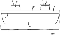
- Figure 4 is a cross section through the portion 2* of the gate electrode layer 2 between a source contact 3 and a body contact 5. It shows the substrate 1 with the body well 11 and the gate electrode layer 2, which is arranged on the gate dielectric 10. Figure 4 also shows part of the intermetal dielectric 9, on which the first portion 7 of the first metal layer is applied. The source region 12 and the body contact region 15 are not shown in Figure 4 , because the portion 2* of the gate electrode layer 2 does not overlap with the source region 12 and the body contact region 15.
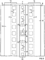
- Figure 5 is a section of a top view according to Figure 1 including a second metal layer.
- the first portion 7 of the first metal layer is connected to a first portion 19 of the second metal layer by a plurality of first vias 17, which are vertical electric interconnections between the first and second metal layers.
- the second portion 8 of the first metal layer is connected to a second portion 20 of the second metal layer by a second via 18 or by a plurality of second vias 18.
- the first metal layer 7, 8 is assumed to be covered with the intermetal dielectric 9 and is therefore shown with broken lines, whereas the second metal layer 19, 20 is assumed to be uncovered.
- the positions of the source contacts 3 and the body contact 5 are also indicated.
- Figure 6 is a top view of a larger area of the device including the drain contacts.
- Figure 6 shows the gate electrode layer 2, the source contacts 3, the body contacts 5, the first vias 17, the second vias 18, the first portion 19 of the second metal layer and the second portion 20 of the second metal layer.
- Drain contacts 21 are applied on drain regions 22 in the substrate 1, which are present on two opposite lateral sides of the gate electrode layer 2 in a symmetrical arrangement.
- the drain contacts 21 are arranged on two straight lines, which are parallel and at equal distances from the straight line running through the centres of the source contacts 3 and the body contacts 5.
- the arrangement of the regions is symmetrical.
- the straight line running through the centres of the source contacts 3 and the body contacts 5 is the axis of symmetry.
- the centres of the body contacts 5 are arranged at a distance d from one another.
- the arrangement of a group of source contacts 3 and a body contact 5 or group of body contacts 5 may periodically be repeated along the axis of symmetry, so that the body contacts 5 are regularly arranged between the source contacts 3.
- the described implantation of the body contact region which is self-aligned to the gate electrode layer, reduces the size of the transistor cell and thus increases the number of transistor cells that can be disposed in a limited area.
- the specific on-resistance which is measured in ⁇ mm 2 , is reduced, because the distance of the body contacts from the channel region is smaller than in conventional devices.
Landscapes
- Insulated Gate Type Field-Effect Transistor (AREA)
Abstract
Description
- A field effect transistor cell comprises the areas of source, drain and body including a channel region. In symmetrical field effect transistors, the cell size is defined by the distance from the axis of symmetry of the body region to the axis of symmetry of the drain region. Small cell sizes are especially important in output stages to achieve a small on-resistance. The cell size is reduced if source and body are provided with a common contact, but this excludes the application of different voltages to source and body, which may be required in some designs of integrated circuits.
-
US 8 963 243 discloses a p-channel LDMOS transistor with a semiconductor substrate provided with a well of n-type conductivity. A p-type source region, a p+-type source contact region and an n-type body contact region are arranged in the well. The contact regions are separated by an isolation region and provided with separate contacts. -
US 2015/0123206 A1 discloses a field effect transistor provided with a body-contact. A gate strip is disposed on a first portion of the active region of a substrate. Source and drain regions are disposed on second and third portions of the active region adjacent to opposite sides of the gate strip. A body-contact region is disposed on a fourth portion of the active region separated from the gate strip by a fifth portion of the active region. The fifth portion of the active region is not covered by any silicide features. - It is an object of the present invention to disclose a field effect transistor device with small cell size that allows to apply different electric potentials to source and body, and a method of producing such a device.
- This object is achieved with the field effect transistor device according to
claim 1 and with the method of producing a field effect transistor device according toclaim 10. Embodiments derive from the dependent claims. - The field effect transistor device comprises a substrate of semiconductor material, a body well of a first type of electric conductivity in the substrate, a source region in the body well, the source region having an opposite second type of electric conductivity, a source contact on the source region, a body contact region of the first type of electric conductivity in the body well, a body contact on the body contact region, and a gate electrode layer partially overlapping the body well. A portion of the gate electrode layer is present between the source contact and the body contact.
- In particular, the first type of electric conductivity may be n-type conductivity. In this case, the second type of electric conductivity is p-type conductivity. The first type of electric conductivity may instead be p-type conductivity and the second type of electric conductivity n-type conductivity.
- An embodiment of the device comprises a source spacer and a body spacer at the gate electrode layer. The source spacer is arranged between the gate electrode layer and the source contact, and the body spacer is arranged between the gate electrode layer and the body contact. The body contact may be laterally surrounded by the gate electrode layer.
- In a further embodiment, areas of the substrate under the source spacer and under the body spacer are free from silicide.
- The source contact may be one of a plurality of source contacts, which are arranged on a straight line. The body contact may also be one of a plurality of body contacts arranged on the straight line, and in particular at equal distances from one another. In particular, the same number of the source contacts may be arranged between any two of the body contacts that immediately follow one another in the sequence of body contacts.
- A further embodiment comprises a source extension of the second type of electric conductivity, the source extension extending the source region under the gate electrode layer. The electric conductivity of the source extension is lower than the electric conductivity of the source region. The source extension is embedded in a halo implant of the first type of electric conductivity.
- A further embodiment comprises a first metal layer above the substrate. A first portion of the first metal layer contacts the source contact, and a second portion of the first metal layer contacts the body contact.
- A further embodiment comprises a second metal layer above the first metal layer. The first portion of the first metal layer is connected to a first portion of the second metal layer by a first via, which forms a vertical electric interconnection, or by a plurality of first vias, and the second portion of the first metal layer is connected to a second portion of the second metal layer by a second via or by a plurality of second vias.
- The method of producing a field effect transistor device comprises forming a body well of a first type of electric conductivity in a substrate of semiconductor material, forming a source region in the body well, the source region having an opposite second type of electric conductivity, applying a source contact on the source region, forming a body contact region of the first type of electric conductivity in the body well, applying a body contact on the body contact region, forming a gate electrode layer partially overlapping the body well, and forming a body spacer at the gate electrode layer.
- The body spacer is formed covering an area of the substrate that is free from silicide and surrounding an area provided for the body contact region. The body contact region is formed self-aligned to the gate electrode layer and the body spacer by an implantation of dopant using a mask that has an opening above the region that is provided for the body contact region.
- The gate electrode layer is formed in such a manner that a portion of the gate electrode layer is arranged between the source contact and the body contact. If the body contact is arranged between two source contacts, portions of the gate electrode layer may be arranged between the body contact and each of the source contacts.
- In a variant of the method, a source spacer is formed at the gate electrode layer. The source spacer covers an area of the substrate that is free from silicide and surrounds an area provided for the source region. The source region is formed self-aligned to the gate electrode layer and the source spacer by an implantation of a further dopant.
- In a further variant of the method, a halo implant is formed in an area provided for the source region by an implantation of dopant for the first type of electric conductivity. A source extension is formed in the halo implant by an implantation of dopant for the second type of electric conductivity. The source extension extends the source region under the gate electrode layer towards the channel region. The electric conductivity of the source extension is lower than the electric conductivity of the source region. This is achieved by a lower net doping concentration of the source extension, where the doping for the second type of electric conductivity overcompensates the first type of electric conductivity provided by the body well and the halo implant.
- In a further variant of the method, the implantation of dopant for the second type of electric conductivity that is provided for the source extension is also performed in an area provided for the body contact region. The body contact region is formed by an implantation of dopant for the first type of electric conductivity, which overcompensates the implantation for the second type of conductivity and results in a net doping of the first type of electric conductivity throughout the body contact region.
- In a further variant of the method, the implantation of the body contact region is deeper than the implantation of the source extension.
- The following is a detailed description of examples of the device and the method in conjunction with the appended figures.
- Figure 1
- is a section of a top view of an embodiment of the device including a first metal layer.
- Figure 2
- is a cross section of the device at the location indicated in
Figure 1 with arrows II. - Figure 3
- is a cross section of the device at the location indicated in
Figure 1 with arrows III. - Figure 4
- is a cross section of the device at the location indicated in
Figure 1 with arrows IV. - Figure 5
- is a section of a top view according to
Figure 1 including a second metal layer. - Figure 6
- is a top view of a larger area of the device including the drain contacts.
-
Figure 1 is a section of a top view of an embodiment of the field effect transistor device including only the first metal layer. Hidden contours are represented with broken lines. The field effect transistor device comprises asubstrate 1 of semiconductor material, which may especially be silicon, for instance. A structuredgate electrode layer 2, which may be electrically conductive polysilicon, for instance, is arranged above the surface of thesubstrate 1. A body well is formed in thesubstrate 1. A source region or a plurality of source regions and a body contact region or a plurality of body contact regions are formed in the body well. - At least one
source contact 3 is arranged on the source region, and at least onebody contact 5 is arranged on the body contact region. Thesource contact 3 and thebody contact 5 may in particular be arranged on a straight line in the direction that is vertical inFigure 1 . - The device may comprise a plurality of
source contacts 3, and it may comprise a plurality ofbody contacts 5. In the embodiment according toFigure 1 , only one of thebody contacts 5 is arranged between groups ofsource contacts 3. A group ofbody contacts 5 may instead be arranged betweensource contacts 3. - At least one spacer of dielectric material, which is here referred to as source spacer 4, can be arranged at edges of the
gate electrode layer 2 facing thesource contact 3. Thesource spacer 4 may especially surround a group ofsource contacts 3. There may be a plurality ofsource spacers 4, and each of thesource spacers 4 may surround a separate group ofsource contacts 3. Thesource contacts 3 may be arranged at a small distance from the neighbouringsource spacer 4. - At least one further spacer of dielectric material, which is here referred to as
body spacer 6, can be arranged at further edges of thegate electrode layer 2 facing thebody contact 5. Thebody spacer 6 may surround asingle body contact 5, as shown inFigure 1 , or a group ofbody contacts 5. There may be a plurality ofbody spacers 6, and each of thebody spacers 6 may surround asingle body contact 5 or a group ofbody contacts 5. Thebody contacts 5 may be arranged at a small distance from the neighbouringbody spacer 6. - The
source contact 3 is connected with afirst portion 7 of a first metal layer. If the transistor cell comprises a plurality ofsource contacts 3, eachsource contact 3 is connected with thefirst portion 7 of the first metal layer. Thebody contact 5 is connected with asecond portion 8 of the first metal layer. If the transistor cell comprises a plurality ofbody contacts 5, eachbody contact 5 is connected with thesecond portion 8 of the first metal layer. - In the top view of
Figure 1 , thesource contacts 3 and parts of thesource spacers 4 are covered by thefirst portion 7 of the first metal layer and are therefore shown as hidden contours with broken lines. Similarly, thebody contact 5 is covered by thesecond portion 8 of the first metal layer. Thegate electrode layer 2 is partially covered by thefirst portion 7 of the first metal layer. - Electrically conductive vias may be provided for an electric connection of the
gate electrode layer 2 with a further portion of the first metal layer. In particular, the electrically conductive vias may be arranged outside the active area, especially above an insulating region, which may be formed by a field oxide, for instance. Details of an electric connection of thegate electrode layer 2 are not relevant to the invention and are not shown in the figures. -
Figure 1 shows how the edges of thegate electrode layer 2 facing thesource contacts 3 and thebody contact 5 may be lined with thesource spacers 4 and thebody spacer 6. -
Portions 2* of thegate electrode layer 2 are present between thebody contact 5 and theadjacent source contacts 3. Theseportion 2* of thegate electrode layer 2 allow to implant the body contact region at a distance from the source regions and afterwards separate thebody contact 5 from theadjacent source contacts 3. - The
mask 16, which is used in the implantation of the body contact region, is schematically indicated inFigure 1 . Themask 16 may be applied on thegate electrode layer 2 and on regions of the active area that are not covered by thegate electrode layer 2. Themask 16 comprises an opening above the region that is provided for the body contact region. - In
Figure 1 three locations of cross sections II, III and IV are indicated. These cross sections are respectively shown inFigures 2, 3 and4 , which are described in the following. -
Figure 2 is a cross section through asource contact 3. It shows thesubstrate 1 with the body well 11 and thegate electrode layer 2, which is arranged on agate dielectric 10. The body well 11 is doped for a first type of electric conductivity, which may be n-type conductivity, for instance. Thesource spacer 4 is arranged at the lateral edges of thegate electrode layer 2 facing thesource contact 3. The area of thesubstrate 1 that is covered by thesource spacer 4 is thus prevented from being silicided. A short circuit, which may be due to an uninterrupted silicide layer, is thereby avoided between the contacts.Figure 2 also shows part of anintermetal dielectric 9, on which thefirst portion 7 of the first metal layer is applied. - The
source region 12 is formed in the body well 11. Asource extension 13 of lower doping concentration and hence lower electric conductivity may be provided towards the channel region, which is located under thegate electrode layer 2. Thesource extension 13 is overlapped by thegate electrode layer 2. Thesource region 12 and thesource extension region 13 are doped for the opposite second type of electric conductivity, which may be p-type conductivity, for instance. The types of conductivity may instead be reversed. Ahalo implant 14 for the first type of electric conductivity may be provided for thesource extension 13. An implantation of a moderately doped region in an oppositely doped halo region may also be used to form an LDD (lightly doped drain) region, which extends the drain region towards the channel region. -
Figure 3 is a cross section through abody contact 5. It shows thesubstrate 1 with the body well 11 and thegate electrode layer 2, which is arranged on thegate dielectric 10. Thebody spacer 6 is arranged at the lateral edges of thegate electrode layer 2 facing thebody contact 5. The area of thesubstrate 1 that is covered by thebody spacer 4 is thus also prevented from being silicided.Figure 3 shows part of theintermetal dielectric 9, on which thefirst portion 7 and thesecond portion 8 of the first metal layer are applied. - The
body contact region 15 is formed by an implantation of dopant for the first type of electric conductivity. The implantation of thebody contact region 15 is deeper than thesource extension 13, so that thebody contact region 15 continuously extends into the body well 11, as indicated inFigure 3 by the central broken line. - The
halo implant 14 has the first type of electric conductivity and can be used for thebody contact region 15 as well. It is not necessary to apply a dedicated LDD mask shielding the implantation for thesource extension 13 from thebody contact region 15. Since no mask openings obeying LDD design rules have to be produced, the area of thebody contact region 15 can be made extremely small. The implantation for thebody contact region 15 can be deeper than the implantation of thehalo implant 14, as shown inFigure 3 by way of example, or vice versa. - The
source region 12 and thebody contact region 15 are formed self-aligned to thegate electrode layer 2, including thesource spacers 4 and thebody spacers 6, respectively, as shown inFigures 2 and 3 . Therefore thegate electrode layer 2, and inparticular portion 2* of thegate electrode layer 2 does not overlap with thesource region 12 and thebody contact region 15. The vertically shallower portions of thesource spacers 4 and thebody spacers 6 may not completely shield the implantations, so that the margins of thesource region 12 and thebody contact region 15 may slightly extend under thesource spacers 4 and thebody spacers 6. -
Figure 4 is a cross section through theportion 2* of thegate electrode layer 2 between asource contact 3 and abody contact 5. It shows thesubstrate 1 with the body well 11 and thegate electrode layer 2, which is arranged on thegate dielectric 10.Figure 4 also shows part of theintermetal dielectric 9, on which thefirst portion 7 of the first metal layer is applied. Thesource region 12 and thebody contact region 15 are not shown inFigure 4 , because theportion 2* of thegate electrode layer 2 does not overlap with thesource region 12 and thebody contact region 15. -
Figure 5 is a section of a top view according toFigure 1 including a second metal layer. Thefirst portion 7 of the first metal layer is connected to afirst portion 19 of the second metal layer by a plurality offirst vias 17, which are vertical electric interconnections between the first and second metal layers. Thesecond portion 8 of the first metal layer is connected to asecond portion 20 of the second metal layer by a second via 18 or by a plurality ofsecond vias 18. - In
Figure 5 , thefirst metal layer intermetal dielectric 9 and is therefore shown with broken lines, whereas thesecond metal layer source contacts 3 and thebody contact 5 are also indicated. -
Figure 6 is a top view of a larger area of the device including the drain contacts.Figure 6 shows thegate electrode layer 2, thesource contacts 3, thebody contacts 5, thefirst vias 17, thesecond vias 18, thefirst portion 19 of the second metal layer and thesecond portion 20 of the second metal layer.Drain contacts 21 are applied ondrain regions 22 in thesubstrate 1, which are present on two opposite lateral sides of thegate electrode layer 2 in a symmetrical arrangement. Thedrain contacts 21 are arranged on two straight lines, which are parallel and at equal distances from the straight line running through the centres of thesource contacts 3 and thebody contacts 5. - In the embodiment according to
Figure 6 , the arrangement of the regions is symmetrical. The straight line running through the centres of thesource contacts 3 and thebody contacts 5 is the axis of symmetry. The centres of thebody contacts 5 are arranged at a distance d from one another. The arrangement of a group ofsource contacts 3 and abody contact 5 or group ofbody contacts 5 may periodically be repeated along the axis of symmetry, so that thebody contacts 5 are regularly arranged between thesource contacts 3. - The described implantation of the body contact region, which is self-aligned to the gate electrode layer, reduces the size of the transistor cell and thus increases the number of transistor cells that can be disposed in a limited area. The specific on-resistance, which is measured in Ω·mm2, is reduced, because the distance of the body contacts from the channel region is smaller than in conventional devices.
-
- 1
- substrate
- 2
- gate electrode layer
- 2*
- portion of the gate electrode layer
- 3
- source contact
- 4
- source spacer
- 5
- body contact
- 6
- body spacer
- 7
- first portion of first metal layer
- 8
- second portion of first metal layer
- 9
- intermetal dielectric
- 10
- gate dielectric
- 11
- body well
- 12
- source region
- 13
- source extension
- 14
- halo implant
- 15
- body contact region
- 16
- implantation mask
- 17
- first via
- 18
- second via
- 19
- first portion of second metal layer
- 20
- second portion of second metal layer
- 21
- drain contact
- 22
- drain region
- d
- distance
Claims (14)
- Field effect transistor device, comprising:- a substrate (1) of semiconductor material,- a body well (11) of a first type of electric conductivity in the substrate,- a source region (12) in the body well (11), the source region (12) having an opposite second type of electric conductivity,- a source contact (3) on the source region (12),- a body contact region (15) of the first type of electric conductivity in the body well (11),- a body contact (5) on the body contact region (15), and- a gate electrode layer (2) partially overlapping the body well (11),
characterized in that- a portion (2*) of the gate electrode layer (2) is present between the source contact (3) and the body contact (5). - Field effect transistor device according to claim 1, further comprising:- a source spacer (4) at the gate electrode layer (2), the source spacer (4) being arranged between the gate electrode layer (2) and the source contact (3), and- a body spacer (6) at the gate electrode layer (2), the body spacer (6) being arranged between the gate electrode layer (2) and the body contact (3).
- Field effect transistor device according to claim 2, wherein areas of the substrate (1) under the source spacer (4) and under the body spacer (6) are free from silicide.
- Field effect transistor device according to one of claims 1 to 3, further comprising:- the source contact (3) being one of a plurality of source contacts (3) on a straight line.
- Field effect transistor device according to claim 4, further comprising:- the body contact (5) being one of a plurality of body contacts (5) arranged on the straight line at a distance (d) from one another, and- the same number of the source contacts (3) being arranged between any two of the body contacts (5) that are spaced apart at the distance (d) from one another.
- Field effect transistor device according to one of claims 1 to 5, further comprising:- a source extension (13) of the second type of electric conductivity, the source extension (13) extending the source region (12) under the gate electrode layer (2), the electric conductivity of the source extension (13) being lower than the electric conductivity of the source region (12), and- a halo implant (14) of the first type of electric conductivity, the source extension (13) being embedded in the halo implant (14).
- Field effect transistor device according to one of claims 1 to 6, wherein the body contact (5) is laterally surrounded by the gate electrode layer (2).
- Field effect transistor device according to one of claims 1 to 7, further comprising:- a first metal layer (7, 8),- a first portion (7) of the first metal layer contacting the source contact (3), and- a second portion (8) of the first metal layer contacting the body contact (5).
- Field effect transistor device according to claim 8, further comprising:- a second metal layer (19, 20),- the first portion (7) of the first metal layer being connected to a first portion (19) of the second metal layer by a first via (17), and- the second portion (8) of the first metal layer being connected to a second portion (20) of the second metal layer by a second via (18).
- Method of producing a field effect transistor device, comprising:- forming a body well (11) of a first type of electric conductivity in a substrate (1) of semiconductor material,- forming a source region (12) in the body well (11), the source region (12) having an opposite second type of electric conductivity,- applying a source contact (3) on the source region (12),- forming a body contact region (15) of the first type of electric conductivity in the body well (11),- applying a body contact (5) on the body contact region (15),- forming a gate electrode layer (2) partially overlapping the body well (11), and- forming a body spacer (6) at the gate electrode layer (2), characterized in that- the gate electrode layer (2) is formed with a portion (2*) of the gate electrode layer (2) being present between the source contact (3) and the body contact (5),- the body spacer (6) is formed covering an area of the substrate (1) that is free from silicide and surrounding an area provided for the body contact region (15), and- the body contact region (15) is formed self-aligned to the gate electrode layer (2) and the body spacer (6) by an implantation of dopant.
- Method of producing a field effect transistor device according to claim 10, further comprising:- forming a source spacer (4) at the gate electrode layer (2), the source spacer (4) covering an area of the substrate (1) that is free from silicide and surrounding an area provided for the source region (12), and- forming the source region (12) self-aligned to the gate electrode layer (2) and the source spacer (4) by an implantation of a further dopant.
- Method of producing a field effect transistor device according to claim 10 or 11, further comprising:- forming a halo implant (14) in an area provided for the source region (12) by an implantation of dopant for the first type of electric conductivity, and- forming a source extension (13) in the halo implant (14) by an implantation of dopant for the second type of electric conductivity, the source extension (13) extending the source region (12) under the gate electrode layer (2), the electric conductivity of the source extension (13) being lower than the electric conductivity of the source region (12).
- Method of producing a field effect transistor device according to claim 12, further comprising:- performing the implantation of dopant for the second type of electric conductivity that is provided for the source extension (13) also in an area provided for the body contact region (15), and- forming the body contact region (15) by an implantation of dopant for the first type of electric conductivity, which overcompensates the implantation for the second type of conductivity and results in a net doping of the first type of electric conductivity throughout the body contact region (15).
- Method of producing a field effect transistor device according to claim 13, wherein the implantation of the body contact region (15) is deeper than the implantation of the source extension (13).
Priority Applications (2)
| Application Number | Priority Date | Filing Date | Title |
|---|---|---|---|
| EP16197521.4A EP3319127B1 (en) | 2016-11-07 | 2016-11-07 | Field effect transistor device with separate source and body contacts and method of producing the device |
| US15/803,636 US10283635B2 (en) | 2016-11-07 | 2017-11-03 | Field effect transistor device with separate source and body contacts and method of producing the device |
Applications Claiming Priority (1)
| Application Number | Priority Date | Filing Date | Title |
|---|---|---|---|
| EP16197521.4A EP3319127B1 (en) | 2016-11-07 | 2016-11-07 | Field effect transistor device with separate source and body contacts and method of producing the device |
Publications (2)
| Publication Number | Publication Date |
|---|---|
| EP3319127A1 true EP3319127A1 (en) | 2018-05-09 |
| EP3319127B1 EP3319127B1 (en) | 2020-12-30 |
Family
ID=57256119
Family Applications (1)
| Application Number | Title | Priority Date | Filing Date |
|---|---|---|---|
| EP16197521.4A Active EP3319127B1 (en) | 2016-11-07 | 2016-11-07 | Field effect transistor device with separate source and body contacts and method of producing the device |
Country Status (2)
| Country | Link |
|---|---|
| US (1) | US10283635B2 (en) |
| EP (1) | EP3319127B1 (en) |
Citations (7)
| Publication number | Priority date | Publication date | Assignee | Title |
|---|---|---|---|---|
| US20050151189A1 (en) * | 2003-12-05 | 2005-07-14 | Stmicroelectronics S.R.I. | Shrunk low on-resistance DMOS structure |
| US7405128B1 (en) * | 2007-02-14 | 2008-07-29 | Freescale Semiconductor, Inc. | Dotted channel MOSFET and method |
| US20120049277A1 (en) * | 2010-08-27 | 2012-03-01 | Lin hong-ze | Lateral-diffusion metal-oxide-semiconductor device |
| US20120187483A1 (en) * | 2011-01-26 | 2012-07-26 | Richtek Technology Corporation, R.O.C. | Double diffused metal oxide semiconductor device and manufacturing method thereof |
| US8963243B2 (en) | 2010-07-01 | 2015-02-24 | Ams Ag | P-channel LDMOS transistor and method of producing a p-channel LDMOS transistor |
| US20150123206A1 (en) | 2013-11-04 | 2015-05-07 | Mediatek Inc. | Body-contact metal-oxide-semiconductor field effect transistor device |
| EP3098857A1 (en) * | 2015-05-26 | 2016-11-30 | Nxp B.V. | Field-effect transistors with body dropdowns |
Family Cites Families (4)
| Publication number | Priority date | Publication date | Assignee | Title |
|---|---|---|---|---|
| US7816229B2 (en) * | 2008-09-30 | 2010-10-19 | Infineon Technologies Austria Ag | Semiconductor device with channel stop trench and method |
| JP6252022B2 (en) * | 2013-08-05 | 2017-12-27 | セイコーエプソン株式会社 | Semiconductor device |
| US9536952B2 (en) * | 2014-05-12 | 2017-01-03 | Intersil Americas LLC | Body contact layouts for semiconductor structures |
| US9871135B2 (en) * | 2016-06-02 | 2018-01-16 | Nxp Usa, Inc. | Semiconductor device and method of making |
-
2016
- 2016-11-07 EP EP16197521.4A patent/EP3319127B1/en active Active
-
2017
- 2017-11-03 US US15/803,636 patent/US10283635B2/en active Active
Patent Citations (7)
| Publication number | Priority date | Publication date | Assignee | Title |
|---|---|---|---|---|
| US20050151189A1 (en) * | 2003-12-05 | 2005-07-14 | Stmicroelectronics S.R.I. | Shrunk low on-resistance DMOS structure |
| US7405128B1 (en) * | 2007-02-14 | 2008-07-29 | Freescale Semiconductor, Inc. | Dotted channel MOSFET and method |
| US8963243B2 (en) | 2010-07-01 | 2015-02-24 | Ams Ag | P-channel LDMOS transistor and method of producing a p-channel LDMOS transistor |
| US20120049277A1 (en) * | 2010-08-27 | 2012-03-01 | Lin hong-ze | Lateral-diffusion metal-oxide-semiconductor device |
| US20120187483A1 (en) * | 2011-01-26 | 2012-07-26 | Richtek Technology Corporation, R.O.C. | Double diffused metal oxide semiconductor device and manufacturing method thereof |
| US20150123206A1 (en) | 2013-11-04 | 2015-05-07 | Mediatek Inc. | Body-contact metal-oxide-semiconductor field effect transistor device |
| EP3098857A1 (en) * | 2015-05-26 | 2016-11-30 | Nxp B.V. | Field-effect transistors with body dropdowns |
Also Published As
| Publication number | Publication date |
|---|---|
| US20180130906A1 (en) | 2018-05-10 |
| US10283635B2 (en) | 2019-05-07 |
| EP3319127B1 (en) | 2020-12-30 |
Similar Documents
| Publication | Publication Date | Title |
|---|---|---|
| US9660074B2 (en) | Methods and apparatus for LDMOS devices with cascaded RESURF implants and double buffers | |
| US7602037B2 (en) | High voltage semiconductor devices and methods for fabricating the same | |
| US9852993B2 (en) | Lateral high voltage integrated devices having trench insulation field plates and metal field plates | |
| US9159803B2 (en) | Semiconductor device with HCI protection region | |
| US9276109B2 (en) | High-voltage transistor with high current load capacity and method for its production | |
| US10388741B2 (en) | Semiconductor device with arrangement of semiconductor regions for improving breakdown voltages | |
| US7109562B2 (en) | High voltage laterally double-diffused metal oxide semiconductor | |
| JP5605241B2 (en) | MOS transistor and method for manufacturing semiconductor integrated circuit device | |
| US6888210B2 (en) | Lateral DMOS transistor having reduced surface field | |
| US20170062608A1 (en) | Semiconductor device and method of manufacturing semiconductor device | |
| US9985028B2 (en) | Diluted drift layer with variable stripe widths for power transistors | |
| US9064868B2 (en) | Advanced faraday shield for a semiconductor device | |
| US8803236B1 (en) | Lateral double diffused metal-oxide-semiconductor device and method for fabricating the same | |
| US9184278B2 (en) | Planar vertical DMOS transistor with a conductive spacer structure as gate | |
| US20150162431A1 (en) | Planar vertical dmos transistor with reduced gate charge | |
| US20120049277A1 (en) | Lateral-diffusion metal-oxide-semiconductor device | |
| KR102359373B1 (en) | Method of fabricating a high voltage semiconductor device | |
| US9117901B2 (en) | High voltage device and manufacturing method thereof | |
| US20130207180A1 (en) | Symmetric ldmos transistor and method of production | |
| US20150194424A1 (en) | Semiconductor device and method for manufacturing the same | |
| US8643104B1 (en) | Lateral diffusion metal oxide semiconductor transistor structure | |
| KR100847827B1 (en) | Method of manufacturing a high voltage transistor | |
| KR20110078861A (en) | Horizontal Dimos Transistor | |
| US10283635B2 (en) | Field effect transistor device with separate source and body contacts and method of producing the device | |
| US8598659B2 (en) | Single finger gate transistor |
Legal Events
| Date | Code | Title | Description |
|---|---|---|---|
| PUAI | Public reference made under article 153(3) epc to a published international application that has entered the european phase |
Free format text: ORIGINAL CODE: 0009012 |
|
| STAA | Information on the status of an ep patent application or granted ep patent |
Free format text: STATUS: THE APPLICATION HAS BEEN PUBLISHED |
|
| AK | Designated contracting states |
Kind code of ref document: A1 Designated state(s): AL AT BE BG CH CY CZ DE DK EE ES FI FR GB GR HR HU IE IS IT LI LT LU LV MC MK MT NL NO PL PT RO RS SE SI SK SM TR |
|
| AX | Request for extension of the european patent |
Extension state: BA ME |
|
| STAA | Information on the status of an ep patent application or granted ep patent |
Free format text: STATUS: REQUEST FOR EXAMINATION WAS MADE |
|
| 17P | Request for examination filed |
Effective date: 20180910 |
|
| RBV | Designated contracting states (corrected) |
Designated state(s): AL AT BE BG CH CY CZ DE DK EE ES FI FR GB GR HR HU IE IS IT LI LT LU LV MC MK MT NL NO PL PT RO RS SE SI SK SM TR |
|
| RAP1 | Party data changed (applicant data changed or rights of an application transferred) |
Owner name: AMS AG |
|
| GRAP | Despatch of communication of intention to grant a patent |
Free format text: ORIGINAL CODE: EPIDOSNIGR1 |
|
| STAA | Information on the status of an ep patent application or granted ep patent |
Free format text: STATUS: GRANT OF PATENT IS INTENDED |
|
| RIC1 | Information provided on ipc code assigned before grant |
Ipc: H01L 29/78 20060101ALI20200508BHEP Ipc: H01L 29/06 20060101ALI20200508BHEP Ipc: H01L 29/10 20060101ALI20200508BHEP Ipc: H01L 29/08 20060101ALI20200508BHEP Ipc: H01L 29/423 20060101AFI20200508BHEP |
|
| INTG | Intention to grant announced |
Effective date: 20200612 |
|
| GRAJ | Information related to disapproval of communication of intention to grant by the applicant or resumption of examination proceedings by the epo deleted |
Free format text: ORIGINAL CODE: EPIDOSDIGR1 |
|
| STAA | Information on the status of an ep patent application or granted ep patent |
Free format text: STATUS: REQUEST FOR EXAMINATION WAS MADE |
|
| GRAR | Information related to intention to grant a patent recorded |
Free format text: ORIGINAL CODE: EPIDOSNIGR71 |
|
| GRAS | Grant fee paid |
Free format text: ORIGINAL CODE: EPIDOSNIGR3 |
|
| STAA | Information on the status of an ep patent application or granted ep patent |
Free format text: STATUS: GRANT OF PATENT IS INTENDED |
|
| INTC | Intention to grant announced (deleted) | ||
| RIN1 | Information on inventor provided before grant (corrected) |
Inventor name: PARK, JONG MUN Inventor name: ROEHRER, GEORG Inventor name: KNAIPP, MARTIN |
|
| GRAA | (expected) grant |
Free format text: ORIGINAL CODE: 0009210 |
|
| STAA | Information on the status of an ep patent application or granted ep patent |
Free format text: STATUS: THE PATENT HAS BEEN GRANTED |
|
| INTG | Intention to grant announced |
Effective date: 20201023 |
|
| AK | Designated contracting states |
Kind code of ref document: B1 Designated state(s): AL AT BE BG CH CY CZ DE DK EE ES FI FR GB GR HR HU IE IS IT LI LT LU LV MC MK MT NL NO PL PT RO RS SE SI SK SM TR |
|
| REG | Reference to a national code |
Ref country code: GB Ref legal event code: FG4D |
|
| REG | Reference to a national code |
Ref country code: AT Ref legal event code: REF Ref document number: 1350803 Country of ref document: AT Kind code of ref document: T Effective date: 20210115 |
|
| REG | Reference to a national code |
Ref country code: DE Ref legal event code: R096 Ref document number: 602016050514 Country of ref document: DE |
|
| REG | Reference to a national code |
Ref country code: IE Ref legal event code: FG4D |
|
| PG25 | Lapsed in a contracting state [announced via postgrant information from national office to epo] |
Ref country code: NO Free format text: LAPSE BECAUSE OF FAILURE TO SUBMIT A TRANSLATION OF THE DESCRIPTION OR TO PAY THE FEE WITHIN THE PRESCRIBED TIME-LIMIT Effective date: 20210330 Ref country code: RS Free format text: LAPSE BECAUSE OF FAILURE TO SUBMIT A TRANSLATION OF THE DESCRIPTION OR TO PAY THE FEE WITHIN THE PRESCRIBED TIME-LIMIT Effective date: 20201230 Ref country code: GR Free format text: LAPSE BECAUSE OF FAILURE TO SUBMIT A TRANSLATION OF THE DESCRIPTION OR TO PAY THE FEE WITHIN THE PRESCRIBED TIME-LIMIT Effective date: 20210331 Ref country code: FI Free format text: LAPSE BECAUSE OF FAILURE TO SUBMIT A TRANSLATION OF THE DESCRIPTION OR TO PAY THE FEE WITHIN THE PRESCRIBED TIME-LIMIT Effective date: 20201230 |
|
| REG | Reference to a national code |
Ref country code: AT Ref legal event code: MK05 Ref document number: 1350803 Country of ref document: AT Kind code of ref document: T Effective date: 20201230 |
|
| PG25 | Lapsed in a contracting state [announced via postgrant information from national office to epo] |
Ref country code: SE Free format text: LAPSE BECAUSE OF FAILURE TO SUBMIT A TRANSLATION OF THE DESCRIPTION OR TO PAY THE FEE WITHIN THE PRESCRIBED TIME-LIMIT Effective date: 20201230 Ref country code: BG Free format text: LAPSE BECAUSE OF FAILURE TO SUBMIT A TRANSLATION OF THE DESCRIPTION OR TO PAY THE FEE WITHIN THE PRESCRIBED TIME-LIMIT Effective date: 20210330 Ref country code: LV Free format text: LAPSE BECAUSE OF FAILURE TO SUBMIT A TRANSLATION OF THE DESCRIPTION OR TO PAY THE FEE WITHIN THE PRESCRIBED TIME-LIMIT Effective date: 20201230 |
|
| REG | Reference to a national code |
Ref country code: NL Ref legal event code: MP Effective date: 20201230 |
|
| PG25 | Lapsed in a contracting state [announced via postgrant information from national office to epo] |
Ref country code: HR Free format text: LAPSE BECAUSE OF FAILURE TO SUBMIT A TRANSLATION OF THE DESCRIPTION OR TO PAY THE FEE WITHIN THE PRESCRIBED TIME-LIMIT Effective date: 20201230 |
|
| REG | Reference to a national code |
Ref country code: LT Ref legal event code: MG9D |
|
| PG25 | Lapsed in a contracting state [announced via postgrant information from national office to epo] |
Ref country code: SK Free format text: LAPSE BECAUSE OF FAILURE TO SUBMIT A TRANSLATION OF THE DESCRIPTION OR TO PAY THE FEE WITHIN THE PRESCRIBED TIME-LIMIT Effective date: 20201230 Ref country code: RO Free format text: LAPSE BECAUSE OF FAILURE TO SUBMIT A TRANSLATION OF THE DESCRIPTION OR TO PAY THE FEE WITHIN THE PRESCRIBED TIME-LIMIT Effective date: 20201230 Ref country code: PT Free format text: LAPSE BECAUSE OF FAILURE TO SUBMIT A TRANSLATION OF THE DESCRIPTION OR TO PAY THE FEE WITHIN THE PRESCRIBED TIME-LIMIT Effective date: 20210430 Ref country code: CZ Free format text: LAPSE BECAUSE OF FAILURE TO SUBMIT A TRANSLATION OF THE DESCRIPTION OR TO PAY THE FEE WITHIN THE PRESCRIBED TIME-LIMIT Effective date: 20201230 Ref country code: EE Free format text: LAPSE BECAUSE OF FAILURE TO SUBMIT A TRANSLATION OF THE DESCRIPTION OR TO PAY THE FEE WITHIN THE PRESCRIBED TIME-LIMIT Effective date: 20201230 Ref country code: LT Free format text: LAPSE BECAUSE OF FAILURE TO SUBMIT A TRANSLATION OF THE DESCRIPTION OR TO PAY THE FEE WITHIN THE PRESCRIBED TIME-LIMIT Effective date: 20201230 |
|
| PG25 | Lapsed in a contracting state [announced via postgrant information from national office to epo] |
Ref country code: PL Free format text: LAPSE BECAUSE OF FAILURE TO SUBMIT A TRANSLATION OF THE DESCRIPTION OR TO PAY THE FEE WITHIN THE PRESCRIBED TIME-LIMIT Effective date: 20201230 Ref country code: AT Free format text: LAPSE BECAUSE OF FAILURE TO SUBMIT A TRANSLATION OF THE DESCRIPTION OR TO PAY THE FEE WITHIN THE PRESCRIBED TIME-LIMIT Effective date: 20201230 |
|
| PG25 | Lapsed in a contracting state [announced via postgrant information from national office to epo] |
Ref country code: IS Free format text: LAPSE BECAUSE OF FAILURE TO SUBMIT A TRANSLATION OF THE DESCRIPTION OR TO PAY THE FEE WITHIN THE PRESCRIBED TIME-LIMIT Effective date: 20210430 |
|
| REG | Reference to a national code |
Ref country code: DE Ref legal event code: R097 Ref document number: 602016050514 Country of ref document: DE |
|
| PG25 | Lapsed in a contracting state [announced via postgrant information from national office to epo] |
Ref country code: IT Free format text: LAPSE BECAUSE OF FAILURE TO SUBMIT A TRANSLATION OF THE DESCRIPTION OR TO PAY THE FEE WITHIN THE PRESCRIBED TIME-LIMIT Effective date: 20201230 Ref country code: AL Free format text: LAPSE BECAUSE OF FAILURE TO SUBMIT A TRANSLATION OF THE DESCRIPTION OR TO PAY THE FEE WITHIN THE PRESCRIBED TIME-LIMIT Effective date: 20201230 |
|
| PLBE | No opposition filed within time limit |
Free format text: ORIGINAL CODE: 0009261 |
|
| STAA | Information on the status of an ep patent application or granted ep patent |
Free format text: STATUS: NO OPPOSITION FILED WITHIN TIME LIMIT |
|
| PG25 | Lapsed in a contracting state [announced via postgrant information from national office to epo] |
Ref country code: DK Free format text: LAPSE BECAUSE OF FAILURE TO SUBMIT A TRANSLATION OF THE DESCRIPTION OR TO PAY THE FEE WITHIN THE PRESCRIBED TIME-LIMIT Effective date: 20201230 |
|
| 26N | No opposition filed |
Effective date: 20211001 |
|
| PG25 | Lapsed in a contracting state [announced via postgrant information from national office to epo] |
Ref country code: ES Free format text: LAPSE BECAUSE OF FAILURE TO SUBMIT A TRANSLATION OF THE DESCRIPTION OR TO PAY THE FEE WITHIN THE PRESCRIBED TIME-LIMIT Effective date: 20201230 |
|
| PG25 | Lapsed in a contracting state [announced via postgrant information from national office to epo] |
Ref country code: SI Free format text: LAPSE BECAUSE OF FAILURE TO SUBMIT A TRANSLATION OF THE DESCRIPTION OR TO PAY THE FEE WITHIN THE PRESCRIBED TIME-LIMIT Effective date: 20201230 |
|
| PG25 | Lapsed in a contracting state [announced via postgrant information from national office to epo] |
Ref country code: IS Free format text: LAPSE BECAUSE OF FAILURE TO SUBMIT A TRANSLATION OF THE DESCRIPTION OR TO PAY THE FEE WITHIN THE PRESCRIBED TIME-LIMIT Effective date: 20210430 |
|
| PG25 | Lapsed in a contracting state [announced via postgrant information from national office to epo] |
Ref country code: MC Free format text: LAPSE BECAUSE OF FAILURE TO SUBMIT A TRANSLATION OF THE DESCRIPTION OR TO PAY THE FEE WITHIN THE PRESCRIBED TIME-LIMIT Effective date: 20201230 |
|
| REG | Reference to a national code |
Ref country code: CH Ref legal event code: PL |
|
| GBPC | Gb: european patent ceased through non-payment of renewal fee |
Effective date: 20211107 |
|
| PG25 | Lapsed in a contracting state [announced via postgrant information from national office to epo] |
Ref country code: LU Free format text: LAPSE BECAUSE OF NON-PAYMENT OF DUE FEES Effective date: 20211107 Ref country code: BE Free format text: LAPSE BECAUSE OF NON-PAYMENT OF DUE FEES Effective date: 20211130 |
|
| REG | Reference to a national code |
Ref country code: BE Ref legal event code: MM Effective date: 20211130 |
|
| PG25 | Lapsed in a contracting state [announced via postgrant information from national office to epo] |
Ref country code: LI Free format text: LAPSE BECAUSE OF NON-PAYMENT OF DUE FEES Effective date: 20211130 Ref country code: CH Free format text: LAPSE BECAUSE OF NON-PAYMENT OF DUE FEES Effective date: 20211130 |
|
| PG25 | Lapsed in a contracting state [announced via postgrant information from national office to epo] |
Ref country code: IE Free format text: LAPSE BECAUSE OF NON-PAYMENT OF DUE FEES Effective date: 20211107 Ref country code: GB Free format text: LAPSE BECAUSE OF NON-PAYMENT OF DUE FEES Effective date: 20211107 |
|
| PG25 | Lapsed in a contracting state [announced via postgrant information from national office to epo] |
Ref country code: FR Free format text: LAPSE BECAUSE OF NON-PAYMENT OF DUE FEES Effective date: 20211130 |
|
| PG25 | Lapsed in a contracting state [announced via postgrant information from national office to epo] |
Ref country code: HU Free format text: LAPSE BECAUSE OF FAILURE TO SUBMIT A TRANSLATION OF THE DESCRIPTION OR TO PAY THE FEE WITHIN THE PRESCRIBED TIME-LIMIT; INVALID AB INITIO Effective date: 20161107 |
|
| PG25 | Lapsed in a contracting state [announced via postgrant information from national office to epo] |
Ref country code: NL Free format text: LAPSE BECAUSE OF NON-PAYMENT OF DUE FEES Effective date: 20201230 Ref country code: CY Free format text: LAPSE BECAUSE OF FAILURE TO SUBMIT A TRANSLATION OF THE DESCRIPTION OR TO PAY THE FEE WITHIN THE PRESCRIBED TIME-LIMIT Effective date: 20201230 |
|
| PG25 | Lapsed in a contracting state [announced via postgrant information from national office to epo] |
Ref country code: SM Free format text: LAPSE BECAUSE OF FAILURE TO SUBMIT A TRANSLATION OF THE DESCRIPTION OR TO PAY THE FEE WITHIN THE PRESCRIBED TIME-LIMIT Effective date: 20201230 |
|
| P01 | Opt-out of the competence of the unified patent court (upc) registered |
Effective date: 20230822 |
|
| PG25 | Lapsed in a contracting state [announced via postgrant information from national office to epo] |
Ref country code: MK Free format text: LAPSE BECAUSE OF FAILURE TO SUBMIT A TRANSLATION OF THE DESCRIPTION OR TO PAY THE FEE WITHIN THE PRESCRIBED TIME-LIMIT Effective date: 20201230 |
|
| PG25 | Lapsed in a contracting state [announced via postgrant information from national office to epo] |
Ref country code: MT Free format text: LAPSE BECAUSE OF FAILURE TO SUBMIT A TRANSLATION OF THE DESCRIPTION OR TO PAY THE FEE WITHIN THE PRESCRIBED TIME-LIMIT Effective date: 20201230 |
|
| REG | Reference to a national code |
Ref country code: DE Ref legal event code: R079 Ref document number: 602016050514 Country of ref document: DE Free format text: PREVIOUS MAIN CLASS: H01L0029423000 Ipc: H10D0064270000 |
|
| PG25 | Lapsed in a contracting state [announced via postgrant information from national office to epo] |
Ref country code: TR Free format text: LAPSE BECAUSE OF FAILURE TO SUBMIT A TRANSLATION OF THE DESCRIPTION OR TO PAY THE FEE WITHIN THE PRESCRIBED TIME-LIMIT Effective date: 20201230 |
|
| PGFP | Annual fee paid to national office [announced via postgrant information from national office to epo] |
Ref country code: DE Payment date: 20251119 Year of fee payment: 10 |