EP3319124A1 - Method and circuit for integrated circuit body biasing - Google Patents
Method and circuit for integrated circuit body biasing Download PDFInfo
- Publication number
- EP3319124A1 EP3319124A1 EP17168139.8A EP17168139A EP3319124A1 EP 3319124 A1 EP3319124 A1 EP 3319124A1 EP 17168139 A EP17168139 A EP 17168139A EP 3319124 A1 EP3319124 A1 EP 3319124A1
- Authority
- EP
- European Patent Office
- Prior art keywords
- circuit
- type
- biasing
- domain
- domains
- Prior art date
- Legal status (The legal status is an assumption and is not a legal conclusion. Google has not performed a legal analysis and makes no representation as to the accuracy of the status listed.)
- Pending
Links
Images


Classifications
-
- H—ELECTRICITY
- H10—SEMICONDUCTOR DEVICES; ELECTRIC SOLID-STATE DEVICES NOT OTHERWISE PROVIDED FOR
- H10D—INORGANIC ELECTRIC SEMICONDUCTOR DEVICES
- H10D84/00—Integrated devices formed in or on semiconductor substrates that comprise only semiconducting layers, e.g. on Si wafers or on GaAs-on-Si wafers
- H10D84/80—Integrated devices formed in or on semiconductor substrates that comprise only semiconducting layers, e.g. on Si wafers or on GaAs-on-Si wafers characterised by the integration of at least one component covered by groups H10D12/00 or H10D30/00, e.g. integration of IGFETs
- H10D84/82—Integrated devices formed in or on semiconductor substrates that comprise only semiconducting layers, e.g. on Si wafers or on GaAs-on-Si wafers characterised by the integration of at least one component covered by groups H10D12/00 or H10D30/00, e.g. integration of IGFETs of only field-effect components
- H10D84/83—Integrated devices formed in or on semiconductor substrates that comprise only semiconducting layers, e.g. on Si wafers or on GaAs-on-Si wafers characterised by the integration of at least one component covered by groups H10D12/00 or H10D30/00, e.g. integration of IGFETs of only field-effect components of only insulated-gate FETs [IGFET]
- H10D84/85—Complementary IGFETs, e.g. CMOS
- H10D84/859—Complementary IGFETs, e.g. CMOS comprising both N-type and P-type wells, e.g. twin-tub
-
- H—ELECTRICITY
- H03—ELECTRONIC CIRCUITRY
- H03K—PULSE TECHNIQUE
- H03K17/00—Electronic switching or gating, i.e. not by contact-making and –breaking
- H03K17/28—Modifications for introducing a time delay before switching
- H03K17/284—Modifications for introducing a time delay before switching in field effect transistor switches
-
- G—PHYSICS
- G01—MEASURING; TESTING
- G01R—MEASURING ELECTRIC VARIABLES; MEASURING MAGNETIC VARIABLES
- G01R31/00—Arrangements for testing electric properties; Arrangements for locating electric faults; Arrangements for electrical testing characterised by what is being tested not provided for elsewhere
- G01R31/28—Testing of electronic circuits, e.g. by signal tracer
- G01R31/317—Testing of digital circuits
- G01R31/31725—Timing aspects, e.g. clock distribution, skew, propagation delay
-
- H—ELECTRICITY
- H03—ELECTRONIC CIRCUITRY
- H03K—PULSE TECHNIQUE
- H03K17/00—Electronic switching or gating, i.e. not by contact-making and –breaking
- H03K17/51—Electronic switching or gating, i.e. not by contact-making and –breaking characterised by the components used
- H03K17/56—Electronic switching or gating, i.e. not by contact-making and –breaking characterised by the components used by the use, as active elements, of semiconductor devices
- H03K17/687—Electronic switching or gating, i.e. not by contact-making and –breaking characterised by the components used by the use, as active elements, of semiconductor devices the devices being field-effect transistors
- H03K17/693—Switching arrangements with several input- or output-terminals, e.g. multiplexers, distributors
-
- H—ELECTRICITY
- H03—ELECTRONIC CIRCUITRY
- H03K—PULSE TECHNIQUE
- H03K19/00—Logic circuits, i.e. having at least two inputs acting on one output; Inverting circuits
- H03K19/003—Modifications for increasing the reliability for protection
- H03K19/00315—Modifications for increasing the reliability for protection in field-effect transistor circuits
-
- H—ELECTRICITY
- H03—ELECTRONIC CIRCUITRY
- H03K—PULSE TECHNIQUE
- H03K19/00—Logic circuits, i.e. having at least two inputs acting on one output; Inverting circuits
- H03K19/02—Logic circuits, i.e. having at least two inputs acting on one output; Inverting circuits using specified components
- H03K19/08—Logic circuits, i.e. having at least two inputs acting on one output; Inverting circuits using specified components using semiconductor devices
- H03K19/094—Logic circuits, i.e. having at least two inputs acting on one output; Inverting circuits using specified components using semiconductor devices using field-effect transistors
-
- H—ELECTRICITY
- H03—ELECTRONIC CIRCUITRY
- H03K—PULSE TECHNIQUE
- H03K19/00—Logic circuits, i.e. having at least two inputs acting on one output; Inverting circuits
- H03K19/20—Logic circuits, i.e. having at least two inputs acting on one output; Inverting circuits characterised by logic function, e.g. AND, OR, NOR, NOT circuits
- H03K19/21—EXCLUSIVE-OR circuits, i.e. giving output if input signal exists at only one input; COINCIDENCE circuits, i.e. giving output only if all input signals are identical
-
- H—ELECTRICITY
- H03—ELECTRONIC CIRCUITRY
- H03K—PULSE TECHNIQUE
- H03K3/00—Circuits for generating electric pulses; Monostable, bistable or multistable circuits
- H03K3/02—Generators characterised by the type of circuit or by the means used for producing pulses
- H03K3/027—Generators characterised by the type of circuit or by the means used for producing pulses by the use of logic circuits, with internal or external positive feedback
- H03K3/037—Bistable circuits
-
- H—ELECTRICITY
- H10—SEMICONDUCTOR DEVICES; ELECTRIC SOLID-STATE DEVICES NOT OTHERWISE PROVIDED FOR
- H10D—INORGANIC ELECTRIC SEMICONDUCTOR DEVICES
- H10D62/00—Semiconductor bodies, or regions thereof, of devices having potential barriers
- H10D62/10—Shapes, relative sizes or dispositions of the regions of the semiconductor bodies; Shapes of the semiconductor bodies
- H10D62/17—Semiconductor regions connected to electrodes not carrying current to be rectified, amplified or switched, e.g. channel regions
- H10D62/351—Substrate regions of field-effect devices
- H10D62/357—Substrate regions of field-effect devices of FETs
- H10D62/364—Substrate regions of field-effect devices of FETs of IGFETs
- H10D62/371—Inactive supplementary semiconductor regions, e.g. for preventing punch-through, improving capacity effect or leakage current
-
- H—ELECTRICITY
- H10—SEMICONDUCTOR DEVICES; ELECTRIC SOLID-STATE DEVICES NOT OTHERWISE PROVIDED FOR
- H10D—INORGANIC ELECTRIC SEMICONDUCTOR DEVICES
- H10D84/00—Integrated devices formed in or on semiconductor substrates that comprise only semiconducting layers, e.g. on Si wafers or on GaAs-on-Si wafers
- H10D84/01—Manufacture or treatment
- H10D84/0123—Integrating together multiple components covered by H10D12/00 or H10D30/00, e.g. integrating multiple IGBTs
- H10D84/0126—Integrating together multiple components covered by H10D12/00 or H10D30/00, e.g. integrating multiple IGBTs the components including insulated gates, e.g. IGFETs
- H10D84/0165—Integrating together multiple components covered by H10D12/00 or H10D30/00, e.g. integrating multiple IGBTs the components including insulated gates, e.g. IGFETs the components including complementary IGFETs, e.g. CMOS devices
- H10D84/0191—Manufacturing their doped wells
-
- H—ELECTRICITY
- H10—SEMICONDUCTOR DEVICES; ELECTRIC SOLID-STATE DEVICES NOT OTHERWISE PROVIDED FOR
- H10D—INORGANIC ELECTRIC SEMICONDUCTOR DEVICES
- H10D84/00—Integrated devices formed in or on semiconductor substrates that comprise only semiconducting layers, e.g. on Si wafers or on GaAs-on-Si wafers
- H10D84/01—Manufacture or treatment
- H10D84/02—Manufacture or treatment characterised by using material-based technologies
- H10D84/03—Manufacture or treatment characterised by using material-based technologies using Group IV technology, e.g. silicon technology or silicon-carbide [SiC] technology
- H10D84/038—Manufacture or treatment characterised by using material-based technologies using Group IV technology, e.g. silicon technology or silicon-carbide [SiC] technology using silicon technology, e.g. SiGe
Definitions
- the present disclosure relates to the field of integrated circuits, and in particular to a circuit and method for applying body biasing voltages to n-type and p-type wells of an integrated circuit.
- FBB forward body biasing
- RTB reverse body biasing
- an integrated circuit comprising: a plurality of circuit domains, each circuit domain comprising: a plurality of transistor devices positioned over p-type and n-type wells, the transistor devices defining one or more data paths of the circuit domain; a monitoring circuit adapted to detect when the slack time of at least one of the data paths in the circuit domain falls below a threshold level and to generate an output signal on an output line based on said detection; and a biasing circuit adapted to modify a biasing voltage of the n-type and/or p-type well of the circuit domain.
- each circuit domain comprises a plurality of p-type wells electrically coupled together and a plurality of n-type wells electrically coupled together.
- the biasing circuit is coupled to the output line of the monitoring circuit and adapted to modify the biasing voltage based on said output signal.
- the output lines of the monitoring circuits of the plurality of circuit domains are coupled to a control circuit, and the control circuit is adapted to control the biasing circuit of each circuit domain to modify the biasing voltages based on the output signals from each monitoring circuit.
- the biasing circuit comprises a switch having a plurality of inputs coupled to corresponding supply voltage rails, and an output coupled via a well tap to the n-type or p-type well, the switch being controlled by said output signal to select one of the supply voltage rails to be coupled to the well tap.
- the monitoring circuit comprises: a flip-flop having a data input coupled to the at least one data path and receiving a clock signal; and a circuit adapted to assert the output signal if a transition of a data signal in said at least one data path occurs within a first time period of a clock edge of said clock signal.
- the n-type and p-type wells extend across the plurality of circuit domains.
- an insulating strip is positioned between one or more n-type wells of a first of the circuit domains and one or more n-type wells of a second of the circuit domains, and between one or more p-type wells of the first of the circuit domains and one or more p-type wells of the second of the circuit domains.
- each circuit domain comprises a well of the first conductivity type enclosing a well of the second conductivity type.
- a method comprising: detecting, by a monitoring circuit in each of a plurality of circuit domains of an integrated circuit, when a slack time of at least one data path in the circuit domain falls below a threshold level and generating an output signal on an output line based on said detection, wherein each circuit domain comprises a plurality of transistor devices positioned over p-type and n-type wells, the transistor devices defining one or more data paths of the circuit domain; and modifying, by a biasing circuit of each circuit domain, a biasing voltage of the n-type and/or p-type well of the circuit domain.
- connection is used to designate a direct connection between circuit elements
- coupled is used to designate a connection that may be direct, or may be via one or more intermediate elements such as resistors, capacitors or transistors.
- approximately is used to designate a tolerance of plus or minus 10 percent of the value in question.
- Figure 1 is a plan view of a portion of an integrated circuit 100 comprising circuit domains 102, 104, 106 and 108. While an example has been illustrated having four circuit domains arranged in a two-by-two block, in alternative embodiments there could be any plurality of circuit domains arranged in any manner.
- the integrated circuit comprises transistor devices (not shown in Figure 1 ) formed across the device, over corresponding p-type wells (PWELL) and n-type wells (NWELL). These wells are respectively labelled P and N in Figure 1 , and are for example in the form of rows across the integrated circuit that are alternatively of p and n type.
- the integrated circuit 100 has an SOI structure, the transistors being formed in a thin film of silicon separated from a silicon substrate by an insulating layer. The rows of p-type and n-type silicon forming the wells are formed within this silicon substrate.
- Each circuit domain 102 to 108 comprises a biasing circuit 110 having a well tap 112 coupled to one of the NWELLs of the circuit and a further well tap 114 coupled to one of the PWELLs of the circuit domain.
- the biasing circuit 110 is for example adapted to modify a biasing voltage of the n-type and/or p-type well of the circuit domain.
- each circuit domain 102 to 108 for example comprises a monitoring circuit 116 adapted to detect when the slack time of at least one of the data paths in the circuit domain falls below a threshold level.
- the biasing circuit 110 of each circuit domain is adapted to select a back biasing voltage to be applied to the PWELLs and NWELLs of the circuit domain based on the detection performed by the monitoring circuits 116.
- the monitoring circuits 116 in each circuit domain 102 to 108 may detect when the slack time falls below a threshold level, for example due to an increase in the operating temperature of the device, an increase in the clock frequency, and/or a reduction in the supply voltage.
- the corresponding biasing circuit 110 may modify the back biasing voltage of the affected circuit domains in order to increase the slack time.
- each circuit domain has an autonomous circuit for modifying its back biasing voltages independently of the other circuit domains.
- a control circuit 118 may be provided, for example implemented in one of the circuit domains 102 to 108 or elsewhere in the integrated circuit.
- the control circuit 118 is coupled to the output lines of the monitoring circuit 116 of each circuit domain, and has outputs coupled to each of the biasing circuits 110 in order to control the biasing voltage to be applied.
- a centralized approach is used for selecting the biasing voltage to be applied by each biasing circuit. This can for example be advantageous in order to avoid large voltage differences between the back biasing voltages applied to adjacent circuit domains, or in order to limit the overall power consumption of the integrated circuit by only allowing a certain number of circuit domains to be biased with relatively high voltages.
- a circuit domain is a region of the circuit in which the biasing voltage of the PWELLs and NWELLs are controlled, at least to some extent, by a given biasing circuit.
- the PWELLs of each circuit domain are electrically coupled together, such that they have a relatively uniform biasing voltage
- the NWELLs of each circuit domain are electrically coupled together, such that they have a relatively uniform biasing voltage.
- the NWELLs and PWELLs of each circuit domain may be electrically isolated from those of adjacent circuit domains, such that the biasing voltages applied to these PWELLs and NWELLs will have little or no influence on the PWELLs and NWELLs of adjacent circuit domains.
- the PWELLs and NWELLs may be continuous across several circuit domains, but the resistance of the wells means that there will be a voltage gradient between portions of the wells of adjacent circuit domains if different biasing voltages are applied to these domains.
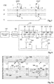
- FIG. 2 schematically illustrates an example of a monitoring circuit 116 of Figure 1 in more detail according to an example embodiment.
- the monitoring circuit 116 is for example coupled in a critical data path of the circuit domain. Indeed, critical paths are the first to have timing violations when the operating environment becomes more challenging, such as due to an increase in the clock frequency or a reduction in the supply voltage. For example, static timing analysis techniques can be used to determine the critical paths in the circuit design, so that monitoring circuits can be placed accordingly.
- the monitoring circuit 116 for example comprises a flip-flop 202 forming part of the critical data path, which is for example a D-type flip-flop.
- the flip-flop 202 is clocked by a clock signal CLK.
- the output signal Q of the flip-flop 202 is for example coupled to one input of an XOR gate 204.
- the data line coupled to the input of the flip-flop 202 is also for example coupled, via a delay circuit 206, to a data input of a further shadow flip-flop 208, which is also for example a D-type flip-flop.
- the delay circuit 206 for example comprises a series connection of delay elements, such as buffers.
- the delayed signal at the output of the delay circuit 206 is labelled D'.
- the flip-flop 208 is clocked by the clock signal CLK, and generates an output signal Q', which is for example coupled to another input of the XOR gate 204.
- the XOR gate 204 provides an early warning signal E that indicates when a slack time on the critical path has fallen below a threshold. This will be described now in more detail with reference to Figure 3 .
- Figure 3 is a timing diagram illustrating examples of the clock signal CLK, the data signals D and D' and the early warning signal E.
- a first transition of the data signal D in the example of Figure 3 occurs a time t1 before a rising edge of the clock signal CLK.
- the slack time tslack is equal to t1-ts. If this slack time falls below zero, a timing violation will occur as the setup time of the flip-flop will no longer be respected, and the output data will become unstable.
- this slack time tslack has a greater duration than the delay d introduced by the delay circuit 206.
- a first transition of the signal D' also respects the setup time ts of the flip-flop 208, which for example has the same setup time as the flip-flop 202.
- the signals Q and Q' will have the same value, and as a consequence, the output of the XOR gate 204 remains at "0", meaning that the signal E remains low and there is no early warning.
- a second transition of the data signal D in the example of Figure 3 occurs a time t2 before a subsequent rising edge of the clock signal CLK.
- the slack time tslack' is now equal to t2-ts, and has a shorter duration than the delay d introduced by the delay circuit 206.
- the second transition of the signal D' does not respect the setup time ts of the flip-flop 208, and the output signal Q' of the flip-flop 208 does not transition.
- the signals Q and Q' at the inputs of the XOR gate 204 are not equal, and the early warning signal E is asserted.
- the biasing circuit 110 of the circuit domain is controlled to increase the back biasing voltage applied to the NWELLs and PWELLs of the circuit domain.
- Figure 4 schematically illustrates the biasing circuit 110 of one of the circuit domains according to an example embodiment.
- the biasing circuit 110 for example comprises switching circuits 402 and 403 each coupled to a plurality n of supply voltage rails having different voltage levels.
- RVT regular threshold voltage
- the PWELLs of NMOS transistors are for example biased at 0 V
- the NWELLs of PMOS transistors are for example biased at the supply voltage Vdd.
- Reverse body biasing (RBB) can be applied to such transistors, involving applying a body biasing voltage to the PWELLs of -Vrbb and/or a body biasing voltage to the NWELLs of Vdd+Vrbb', where Vrbb and Vrbb' may be different.
- Figure 4 assumes a case in which the transistors to be back biased are LVT transistors.
- the switching circuit 402 is a three-path switch coupled to three supply rails, which are respectively at 0 V, 0.3 V and 0.6 V.
- the switching circuit 402 has an output 404 coupled to an NWELL 406 of the circuit domain via the well tap 112, which is for example implemented by a diode having its anode coupled to the output 404, and its cathode coupled to the NWELL.
- the switching circuit 402 for example comprises three switches 408, 410 and 412 respectively coupled between the corresponding supply voltage rails and the output 404.
- additional voltage levels could be provided by further supply rails.
- the switching circuit 403 is a three-path switch coupled to three supply rails, which are respectively at 0 V, -0.3 V and -0.6 V.
- the switching circuit 403 has an output 414 coupled to a PWELL 416 of the circuit domain via the well tap 114, which is for example implemented by a diode having its anode coupled to the node 414, and its cathode coupled to the PWELL.
- the switching circuit 403 for example comprises three switches 418, 420 and 422 respectively coupled between the corresponding supply voltage rails and the output 414.
- additional voltage levels could be provided by further supply rails.
- the switching circuits 402 and 403 are for example controlled by a switch control circuit 424, based on a control signal generated by the corresponding monitoring circuit 116, to couple one of the supply rails of switches 408 to 412 to the output 404 and one of the supply rails of switches 418 to 422 to the output 414.
- the switch control circuit 424 is configured to increase the biasing voltage Vfbb by controlling the switching circuit 402 to select a higher biasing voltage and the switching circuit 403 to select a lower (more negative) biasing voltage.
- the switching circuits 402 and 403 could be controlled directly by a control signal generated by the centralized control circuit 118 of Figure 1 .
- Figure 5A is a plan view of portion of an integrated circuit in which only the two circuit domains 102 and 104 are illustrated.
- the circuit domains 102, 104 are surrounded by circuit regions not associated with any circuit domain, and for example having biasing circuits 506 that apply static body biasing voltages to the corresponding PWELLs and NWELLs.
- Each circuit domain 102, 104 for example comprises a monitoring circuit 116 and a biasing circuit 110 as described above. Furthermore, connections 508 are for example formed to electrically connect the PWELLs together within each circuit domain 102, 104, and connections 510 are for example formed to electrically connect the NWELLs together within each circuit domain 102, 104.
- the NWELLs of the circuit domains 102, 104 extend into other regions of the integrated circuit, and similarly, the PWELLs of the circuit domains 102, 104 extend into other regions of the integrated circuit.
- the NWELLs and PWELLs will have a certain resistance, and thus the biasing circuit 110 within each circuit domain will modify the body biasing voltage within the circuit domain despite surrounding PWELLs and NWELLs being connected to static voltages.
- a voltage difference will be present, as will now be described with reference to Figure 5B .
- Figure 5B is a graph illustrating the voltage level in an NWELL of Figure 5A , and in particular the voltage along a portion A-A' of the NWELL passing close to a well tap of the biasing circuit 110 of the circuit domain 102 and a well tap of a further biasing circuit 506.
- the biasing circuit 110 of the domain 102 applies a forward body biasing voltage FBB
- the further biasing circuit 506 applies the ground voltage
- Figure 6A is a plan view of a portion of an integrated circuit according to an alternative embodiment in which insulating strips are used to isolate the circuit domains.
- the circuit domains 102 and 104 are separated by a substrate strip 606, which for example runs perpendicular to the lengths of the PWELLs and NWELLs of the circuit domains 102, 104.
- the NWELL and PWELL insulating strips are for example layer masks that may comprise "NWELL block" and "PWELL block” patterns so that the substrate strip 606 is not subjected to additional doping with respect to the levels in the substrate.
- the substrate being for example of the p-type, this strip 606 is thus also for example of the p-type.
- This strip 606 thus provides electrical isolation between the NWELLs of the circuit domains 102, 104, and introduces an additional resistance R SUB between the PWELLs of the circuit domains 102, 104.
- the substrate strip 606 for example extends to also provide a barrier between the circuit domains 106 and 108, and for example between other circuit domains not illustrated in Figure 6A .
- Figure 6B is a cross-section view of the structure of Figure 6A taken along a portion B-B' of NWELLs of the circuit domains 102, 104 and passing through the substrate strip 606.
- the integrated circuit for example has an SOI structure comprising a layer of silicon 612 formed over a layer of insulator 614.
- the insulator layer 614 is formed over a silicon substrate 616 comprising an NWELL 618 forming part of the circuit domain 102, and an NWELL 620 forming part of the circuit domain 104.
- NWELLs are separated by the substrate strip 606, which for example extends up to the insulator layer 614 and is continuous with the p-type substrate.
- Figure 7 is a plan view of a portion of an integrated circuit according to yet a further example embodiment.
- one of the wells 702 of each circuit domain 102, 104, 106, 108 encloses one or more further wells 704, 706 of the opposite conductivity type, and is surrounded by a well of the opposite conductivity type, in order to isolate the circuit domains from each other.
- the wells 702 are NWELLs that enclose PWELLS 704, 706, and the NWELLS 702 of each circuit domain 102, 104, 106, 108 are separated from each other by a PWELL 708.
- each of the circuit domains could comprise a PWELL enclosing one or more NWELLs, and an NWELL could separate these PWELLs of adjacent circuit domains.
- An advantage of the embodiments described herein is that body biasing may be applied to different circuit domains of an integrated circuit as a function of the particular constraints in that circuit domain. This permits a local improvement of performance to be applied, and a reduction in power consumption in other portions of the integrated circuit having less critical paths.
Landscapes
- Engineering & Computer Science (AREA)
- Physics & Mathematics (AREA)
- General Engineering & Computer Science (AREA)
- Computer Hardware Design (AREA)
- Computing Systems (AREA)
- Mathematical Physics (AREA)
- General Physics & Mathematics (AREA)
- Power Engineering (AREA)
- Semiconductor Integrated Circuits (AREA)
Abstract
Description
- This application claims the priority benefit of French Patent application number
16/60745, filed on November 7, 2016 - The present disclosure relates to the field of integrated circuits, and in particular to a circuit and method for applying body biasing voltages to n-type and p-type wells of an integrated circuit.
- It has been proposed to alter a body biasing voltage of integrated circuits in order to increase performance and/or reduce power consumption. A shift towards SOI (silicon on insulator) based transistor technology makes body biasing a particularly interesting proposition as this technology permits relatively high biasing voltages, for example from as low as -3 V to as high as +3 V, to be applied to the body of the device. In particular, the biasing voltage is applied to the p-type or n-type well underlying each transistor device, sometimes referred to as the back gate. This compares to a more limited body biasing range of -300 mV to +300 mV in the case of bulk transistors.
- For example, forward body biasing (FBB) involves applying a positive back biasing voltage and provides increased performance by increasing the speed of the transistors. Reverse body biasing (RBB) involves applying a negative back biasing voltage and provides reduced leakage currents and thus reduced power consumption.
- Existing techniques for FBB and RBB have drawbacks in terms of complexity and/or lead to relatively poor power consumption for a given performance level.
- It is an aim of embodiments of the present disclosure to at least partially address one or more needs in the prior art.
- According to one aspect, there is provided an integrated circuit comprising: a plurality of circuit domains, each circuit domain comprising: a plurality of transistor devices positioned over p-type and n-type wells, the transistor devices defining one or more data paths of the circuit domain; a monitoring circuit adapted to detect when the slack time of at least one of the data paths in the circuit domain falls below a threshold level and to generate an output signal on an output line based on said detection; and a biasing circuit adapted to modify a biasing voltage of the n-type and/or p-type well of the circuit domain.
- According to one embodiment, each circuit domain comprises a plurality of p-type wells electrically coupled together and a plurality of n-type wells electrically coupled together.
- According to one embodiment, within each circuit domain, the biasing circuit is coupled to the output line of the monitoring circuit and adapted to modify the biasing voltage based on said output signal.
- According to one embodiment, the output lines of the monitoring circuits of the plurality of circuit domains are coupled to a control circuit, and the control circuit is adapted to control the biasing circuit of each circuit domain to modify the biasing voltages based on the output signals from each monitoring circuit.
- According to one embodiment, the biasing circuit comprises a switch having a plurality of inputs coupled to corresponding supply voltage rails, and an output coupled via a well tap to the n-type or p-type well, the switch being controlled by said output signal to select one of the supply voltage rails to be coupled to the well tap.
- According to one embodiment, the monitoring circuit comprises: a flip-flop having a data input coupled to the at least one data path and receiving a clock signal; and a circuit adapted to assert the output signal if a transition of a data signal in said at least one data path occurs within a first time period of a clock edge of said clock signal.
- According to one embodiment, the n-type and p-type wells extend across the plurality of circuit domains.
- According to one embodiment, an insulating strip is positioned between one or more n-type wells of a first of the circuit domains and one or more n-type wells of a second of the circuit domains, and between one or more p-type wells of the first of the circuit domains and one or more p-type wells of the second of the circuit domains.
- According to one embodiment, each circuit domain comprises a well of the first conductivity type enclosing a well of the second conductivity type.
- According to a further aspect, there is provided a method comprising: detecting, by a monitoring circuit in each of a plurality of circuit domains of an integrated circuit, when a slack time of at least one data path in the circuit domain falls below a threshold level and generating an output signal on an output line based on said detection, wherein each circuit domain comprises a plurality of transistor devices positioned over p-type and n-type wells, the transistor devices defining one or more data paths of the circuit domain; and modifying, by a biasing circuit of each circuit domain, a biasing voltage of the n-type and/or p-type well of the circuit domain.
- The foregoing and other features and advantages will become apparent from the following detailed description of embodiments, given by way of illustration and not limitation with reference to the accompanying drawings, in which:
-
Figure 1 is a plan view of part of an integrated circuit according to an example embodiment of the present disclosure; -
Figure 2 schematically illustrates a monitoring circuit of the integrated circuit ofFigure 1 according to an example embodiment of the present disclosure; -
Figure 3 is a timing diagram illustrating an example of signals in the circuit ofFigure 2 according to an example embodiment; -
Figure 4 schematically illustrates a biasing circuit according to an example embodiment of the present disclosure; -
Figure 5A is a plan view of a portion of an integrated circuit according to a further example embodiment; -
Figure 5B is a graph illustrating voltage levels in a well of the circuit ofFigure 5A according to an example embodiment; -
Figure 6A is a plan view of a portion of an integrated circuit according to a further example embodiment of the present disclosure; -
Figure 6B is a cross-section view of part of the circuit ofFigure 6A according to an example embodiment; and -
Figure 7 is a plan view of a portion of an integrated circuit according to yet a further example embodiment. - Throughout the following description, the term "connected" is used to designate a direct connection between circuit elements, whereas the term "coupled" is used to designate a connection that may be direct, or may be via one or more intermediate elements such as resistors, capacitors or transistors. The term "approximately" is used to designate a tolerance of plus or minus 10 percent of the value in question.
-
Figure 1 is a plan view of a portion of anintegrated circuit 100 comprisingcircuit domains - The integrated circuit comprises transistor devices (not shown in
Figure 1 ) formed across the device, over corresponding p-type wells (PWELL) and n-type wells (NWELL). These wells are respectively labelled P and N inFigure 1 , and are for example in the form of rows across the integrated circuit that are alternatively of p and n type. For example, in one embodiment, theintegrated circuit 100 has an SOI structure, the transistors being formed in a thin film of silicon separated from a silicon substrate by an insulating layer. The rows of p-type and n-type silicon forming the wells are formed within this silicon substrate. - Each
circuit domain 102 to 108 comprises abiasing circuit 110 having awell tap 112 coupled to one of the NWELLs of the circuit and afurther well tap 114 coupled to one of the PWELLs of the circuit domain. Thebiasing circuit 110 is for example adapted to modify a biasing voltage of the n-type and/or p-type well of the circuit domain. - Furthermore, each
circuit domain 102 to 108 for example comprises amonitoring circuit 116 adapted to detect when the slack time of at least one of the data paths in the circuit domain falls below a threshold level. Thebiasing circuit 110 of each circuit domain is adapted to select a back biasing voltage to be applied to the PWELLs and NWELLs of the circuit domain based on the detection performed by themonitoring circuits 116. - Thus, during operation of the
integrated circuit 100, themonitoring circuits 116 in eachcircuit domain 102 to 108 may detect when the slack time falls below a threshold level, for example due to an increase in the operating temperature of the device, an increase in the clock frequency, and/or a reduction in the supply voltage. In response, thecorresponding biasing circuit 110 may modify the back biasing voltage of the affected circuit domains in order to increase the slack time. - For example, within each
circuit domain 102 to 108, an output of themonitoring circuit 116 is coupled to thecorresponding biasing circuit 110 in order to control the selection of the body biasing voltage. Thus each circuit domain has an autonomous circuit for modifying its back biasing voltages independently of the other circuit domains. - Alternatively, as represented by a dashed box in
Figure 1 , acontrol circuit 118 may be provided, for example implemented in one of thecircuit domains 102 to 108 or elsewhere in the integrated circuit. Thecontrol circuit 118 is coupled to the output lines of themonitoring circuit 116 of each circuit domain, and has outputs coupled to each of thebiasing circuits 110 in order to control the biasing voltage to be applied. Thus a centralized approach is used for selecting the biasing voltage to be applied by each biasing circuit. This can for example be advantageous in order to avoid large voltage differences between the back biasing voltages applied to adjacent circuit domains, or in order to limit the overall power consumption of the integrated circuit by only allowing a certain number of circuit domains to be biased with relatively high voltages. - As described in more detail below, a circuit domain is a region of the circuit in which the biasing voltage of the PWELLs and NWELLs are controlled, at least to some extent, by a given biasing circuit. In some embodiments, the PWELLs of each circuit domain are electrically coupled together, such that they have a relatively uniform biasing voltage, and the NWELLs of each circuit domain are electrically coupled together, such that they have a relatively uniform biasing voltage. Furthermore, in some embodiments the NWELLs and PWELLs of each circuit domain may be electrically isolated from those of adjacent circuit domains, such that the biasing voltages applied to these PWELLs and NWELLs will have little or no influence on the PWELLs and NWELLs of adjacent circuit domains. Alternatively, the PWELLs and NWELLs may be continuous across several circuit domains, but the resistance of the wells means that there will be a voltage gradient between portions of the wells of adjacent circuit domains if different biasing voltages are applied to these domains.
-
Figure 2 schematically illustrates an example of amonitoring circuit 116 ofFigure 1 in more detail according to an example embodiment. - The
monitoring circuit 116 is for example coupled in a critical data path of the circuit domain. Indeed, critical paths are the first to have timing violations when the operating environment becomes more challenging, such as due to an increase in the clock frequency or a reduction in the supply voltage. For example, static timing analysis techniques can be used to determine the critical paths in the circuit design, so that monitoring circuits can be placed accordingly. - The
monitoring circuit 116 for example comprises a flip-flop 202 forming part of the critical data path, which is for example a D-type flip-flop. The flip-flop 202 is clocked by a clock signal CLK. The output signal Q of the flip-flop 202 is for example coupled to one input of anXOR gate 204. The data line coupled to the input of the flip-flop 202 is also for example coupled, via adelay circuit 206, to a data input of a further shadow flip-flop 208, which is also for example a D-type flip-flop. Thedelay circuit 206 for example comprises a series connection of delay elements, such as buffers. The delayed signal at the output of thedelay circuit 206 is labelled D'. The flip-flop 208 is clocked by the clock signal CLK, and generates an output signal Q', which is for example coupled to another input of theXOR gate 204. - The
XOR gate 204 provides an early warning signal E that indicates when a slack time on the critical path has fallen below a threshold. This will be described now in more detail with reference toFigure 3 . -
Figure 3 is a timing diagram illustrating examples of the clock signal CLK, the data signals D and D' and the early warning signal E. - A first transition of the data signal D in the example of
Figure 3 occurs a time t1 before a rising edge of the clock signal CLK. Assuming that the flip-flop 202 has a setup time ts before the rising edge of the clock signal CLK, the slack time tslack is equal to t1-ts. If this slack time falls below zero, a timing violation will occur as the setup time of the flip-flop will no longer be respected, and the output data will become unstable. In the case of the first transition ofFigure 3 , this slack time tslack has a greater duration than the delay d introduced by thedelay circuit 206. Thus a first transition of the signal D' also respects the setup time ts of the flip-flop 208, which for example has the same setup time as the flip-flop 202. Thus when the data arrives with the slack time tslack, the signals Q and Q' will have the same value, and as a consequence, the output of theXOR gate 204 remains at "0", meaning that the signal E remains low and there is no early warning. - A second transition of the data signal D in the example of
Figure 3 occurs a time t2 before a subsequent rising edge of the clock signal CLK. The slack time tslack' is now equal to t2-ts, and has a shorter duration than the delay d introduced by thedelay circuit 206. Thus the second transition of the signal D' does not respect the setup time ts of the flip-flop 208, and the output signal Q' of the flip-flop 208 does not transition. Thus the signals Q and Q' at the inputs of theXOR gate 204 are not equal, and the early warning signal E is asserted. - In one embodiment, whenever the early warning signal E is asserted by the
monitoring circuit 116 of a circuit domain, the biasingcircuit 110 of the circuit domain is controlled to increase the back biasing voltage applied to the NWELLs and PWELLs of the circuit domain. -
Figure 4 schematically illustrates the biasingcircuit 110 of one of the circuit domains according to an example embodiment. - The biasing
circuit 110 for example comprises switchingcircuits - In the case of regular threshold voltage (RVT) transistors, when no body biasing is applied, the PWELLs of NMOS transistors are for example biased at 0 V, and the NWELLs of PMOS transistors are for example biased at the supply voltage Vdd. Reverse body biasing (RBB) can be applied to such transistors, involving applying a body biasing voltage to the PWELLs of -Vrbb and/or a body biasing voltage to the NWELLs of Vdd+Vrbb', where Vrbb and Vrbb' may be different.
- In the case of low threshold voltage (LVT) transistors (having flipped wells), when no body biasing is applied, the NWELLs of NMOS transistors and the PWELLs of the PMOS transistors are both for example biased at 0 V. Forward body biasing (RBB) can be applied to such transistors, involving applying a body biasing voltage to the NWELLs of +Vfbb and/or a body biasing voltage to the PWELLs of -Vfbb', where Vfbb and Vfbb' may be different.
-
Figure 4 assumes a case in which the transistors to be back biased are LVT transistors. - In the example of
Figure 4 , theswitching circuit 402 is a three-path switch coupled to three supply rails, which are respectively at 0 V, 0.3 V and 0.6 V. Theswitching circuit 402 has anoutput 404 coupled to anNWELL 406 of the circuit domain via thewell tap 112, which is for example implemented by a diode having its anode coupled to theoutput 404, and its cathode coupled to the NWELL. Theswitching circuit 402 for example comprises threeswitches output 404. Of course, in alternative embodiments, additional voltage levels could be provided by further supply rails. - In the example of
Figure 4 , theswitching circuit 403 is a three-path switch coupled to three supply rails, which are respectively at 0 V, -0.3 V and -0.6 V. Theswitching circuit 403 has anoutput 414 coupled to aPWELL 416 of the circuit domain via thewell tap 114, which is for example implemented by a diode having its anode coupled to thenode 414, and its cathode coupled to the PWELL. Theswitching circuit 403 for example comprises threeswitches output 414. Of course, in alternative embodiments, additional voltage levels could be provided by further supply rails. - As illustrated in
Figure 4 , the switchingcircuits switch control circuit 424, based on a control signal generated by thecorresponding monitoring circuit 116, to couple one of the supply rails ofswitches 408 to 412 to theoutput 404 and one of the supply rails ofswitches 418 to 422 to theoutput 414. For example, each time the output signal of themonitoring circuit 116 is asserted, theswitch control circuit 424 is configured to increase the biasing voltage Vfbb by controlling theswitching circuit 402 to select a higher biasing voltage and theswitching circuit 403 to select a lower (more negative) biasing voltage. - In alternative embodiments, the switching
circuits centralized control circuit 118 ofFigure 1 . - The subdivision of the integrated circuit into circuit domains will now be described in more detail with reference to
Figures 5A ,5B, 6A, 6B and 7 . -
Figure 5A is a plan view of portion of an integrated circuit in which only the twocircuit domains Figure 5A , thecircuit domains circuits 506 that apply static body biasing voltages to the corresponding PWELLs and NWELLs. - Each
circuit domain monitoring circuit 116 and abiasing circuit 110 as described above. Furthermore,connections 508 are for example formed to electrically connect the PWELLs together within eachcircuit domain connections 510 are for example formed to electrically connect the NWELLs together within eachcircuit domain - In the example of
Figure 5A , the NWELLs of thecircuit domains circuit domains biasing circuit 110 within each circuit domain will modify the body biasing voltage within the circuit domain despite surrounding PWELLs and NWELLs being connected to static voltages. When a voltage difference is present between the biasing voltage applied to onecircuit domain other circuit domain Figure 5B . -
Figure 5B is a graph illustrating the voltage level in an NWELL ofFigure 5A , and in particular the voltage along a portion A-A' of the NWELL passing close to a well tap of the biasingcircuit 110 of thecircuit domain 102 and a well tap of afurther biasing circuit 506. As illustrated, in the case that the biasingcircuit 110 of thedomain 102 applies a forward body biasing voltage FBB, and thefurther biasing circuit 506 applies the ground voltage, there is for example a voltage gradient in the NWELL falling in a relatively linear fashion between FBB at thebiasing circuit 110 to ground at thebiasing circuit 506. -
Figure 6A is a plan view of a portion of an integrated circuit according to an alternative embodiment in which insulating strips are used to isolate the circuit domains. In this example thecircuit domains substrate strip 606, which for example runs perpendicular to the lengths of the PWELLs and NWELLs of thecircuit domains substrate strip 606 is not subjected to additional doping with respect to the levels in the substrate. The substrate being for example of the p-type, thisstrip 606 is thus also for example of the p-type. Thisstrip 606 thus provides electrical isolation between the NWELLs of thecircuit domains circuit domains substrate strip 606 for example extends to also provide a barrier between thecircuit domains Figure 6A . -
Figure 6B is a cross-section view of the structure ofFigure 6A taken along a portion B-B' of NWELLs of thecircuit domains substrate strip 606. As illustrated, the integrated circuit for example has an SOI structure comprising a layer ofsilicon 612 formed over a layer ofinsulator 614. Theinsulator layer 614 is formed over asilicon substrate 616 comprising anNWELL 618 forming part of thecircuit domain 102, and anNWELL 620 forming part of thecircuit domain 104. These NWELLs are separated by thesubstrate strip 606, which for example extends up to theinsulator layer 614 and is continuous with the p-type substrate. -
Figure 7 is a plan view of a portion of an integrated circuit according to yet a further example embodiment. In the example ofFigure 7 , one of thewells 702 of eachcircuit domain further wells Figure 7 , thewells 702 are NWELLs that enclose PWELLS 704, 706, and theNWELLS 702 of eachcircuit domain PWELL 708. Of course, in alternative embodiments, each of the circuit domains could comprise a PWELL enclosing one or more NWELLs, and an NWELL could separate these PWELLs of adjacent circuit domains. - An advantage of the embodiments described herein is that body biasing may be applied to different circuit domains of an integrated circuit as a function of the particular constraints in that circuit domain. This permits a local improvement of performance to be applied, and a reduction in power consumption in other portions of the integrated circuit having less critical paths.
- Having thus described at least one illustrative embodiment, various alterations, modifications and improvements will readily occur to those skilled in the art. For example, it will be apparent to those skilled in the art that the embodiments described in relation to
Figures 5A ,5B, 6A, 6B and 7 for subdividing an integrated circuit into circuit domains are merely some examples, and that other techniques could be used.
Claims (10)
- An integrated circuit comprising:a plurality of circuit domains (102, 104, 106, 108), each circuit domain comprising:- a plurality of transistor devices positioned over p-type and n-type wells (P,N), the transistor devices defining one or more data paths of the circuit domain;- a monitoring circuit (116) adapted to detect when the slack time of at least one of the data paths in the circuit domain falls below a threshold level and to generate an output signal on an output line based on said detection; and- a biasing circuit (110) adapted to modify a biasing voltage of the n-type and/or p-type well of the circuit domain.
- The integrated circuit of claim 1, wherein each circuit domain comprises a plurality of p-type wells electrically coupled together and a plurality of n-type wells electrically coupled together.
- The integrated circuit of claim 1 or 2, wherein, within each circuit domain, the biasing circuit (110) is coupled to the output line of the monitoring circuit (116) and adapted to modify the biasing voltage based on said output signal.
- The integrated circuit of claim 1 or 2, wherein the output lines of the monitoring circuits (116) of the plurality of circuit domains are coupled to a control circuit (118), and wherein the control circuit (118) is adapted to control the biasing circuit (110) of each circuit domain to modify the biasing voltages based on the output signals from each monitoring circuit (116).
- The integrated circuit of any of claims 1 to 4, wherein the biasing circuit (110) comprises a switch (402, 403) having a plurality of inputs coupled to corresponding supply voltage rails, and an output (404, 414) coupled via a well tap (112, 114) to the n-type or p-type well, the switch (402, 403) being controlled by said output signal to select one of the supply voltage rails to be coupled to the well tap (112, 114).
- The integrated circuit of any of claims 1 to 5, wherein the monitoring circuit (116) comprises:a flip-flop (202) having a data input coupled to the at least one data path and receiving a clock signal (CLK); anda circuit (204, 206, 208) adapted to assert the output signal if a transition of a data signal in said at least one data path occurs within a first time period (d) of a clock edge of said clock signal.
- The integrated circuit of any of claims 1 to 6, wherein said n-type and p-type wells extend across the plurality of circuit domains.
- The integrated circuit of any of claims 1 to 6, wherein an insulating strip (606) is positioned between one or more n-type wells of a first of said circuit domains (102) and one or more n-type wells of a second of said circuit domains (104), and between one or more p-type wells of the first of said circuit domains (102) and one or more p-type wells of the second of said circuit domains (104).
- The integrated circuit of any of claims 1 to 6, wherein each circuit domain comprises a well of the first conductivity type enclosing a well of the second conductivity type.
- A method comprising:detecting, by a monitoring circuit (116) in each of a plurality of circuit domains (102, 104, 106, 108) of an integrated circuit, when a slack time of at least one data path in the circuit domain falls below a threshold level and generating an output signal on an output line based on said detection, wherein each circuit domain comprises a plurality of transistor devices positioned over p-type and n-type wells (P,N), the transistor devices defining one or more data paths of the circuit domain; andmodifying, by a biasing circuit (110) of each circuit domain, a biasing voltage of the n-type and/or p-type well of the circuit domain.
Applications Claiming Priority (1)
| Application Number | Priority Date | Filing Date | Title |
|---|---|---|---|
| FR1660745A FR3058564B1 (en) | 2016-11-07 | 2016-11-07 | METHOD AND CIRCUIT FOR POLARIZING INTEGRATED CIRCUITS |
Publications (1)
| Publication Number | Publication Date |
|---|---|
| EP3319124A1 true EP3319124A1 (en) | 2018-05-09 |
Family
ID=58213204
Family Applications (1)
| Application Number | Title | Priority Date | Filing Date |
|---|---|---|---|
| EP17168139.8A Pending EP3319124A1 (en) | 2016-11-07 | 2017-04-26 | Method and circuit for integrated circuit body biasing |
Country Status (4)
| Country | Link |
|---|---|
| US (2) | US10050037B2 (en) |
| EP (1) | EP3319124A1 (en) |
| CN (2) | CN108075754B (en) |
| FR (1) | FR3058564B1 (en) |
Families Citing this family (1)
| Publication number | Priority date | Publication date | Assignee | Title |
|---|---|---|---|---|
| US12575173B2 (en) * | 2022-08-01 | 2026-03-10 | Qualcomm Incorporated | Integrated circuit cell with dual row, back-to-back, transistor body ties |
Citations (3)
| Publication number | Priority date | Publication date | Assignee | Title |
|---|---|---|---|---|
| EP2330624A1 (en) * | 2009-12-01 | 2011-06-08 | Nxp B.V. | Well structure for body biasing, manufacturing and design method |
| FR3017466A1 (en) * | 2014-02-07 | 2015-08-14 | Commissariat Energie Atomique | METHOD FOR CHARACTERIZING THE OPERATION OF A DIGITAL ELECTRONIC CIRCUIT AND DIGITAL ELECTRONIC CIRCUIT |
| EP3012976A2 (en) * | 2014-10-02 | 2016-04-27 | Nxp B.V. | Timing control with body-bias |
Family Cites Families (7)
| Publication number | Priority date | Publication date | Assignee | Title |
|---|---|---|---|---|
| US6501313B2 (en) * | 2000-12-27 | 2002-12-31 | International Business Machines Corporation | Dynamic duty cycle adjuster |
| JP4090231B2 (en) * | 2001-11-01 | 2008-05-28 | 株式会社ルネサステクノロジ | Semiconductor integrated circuit device |
| JP4401621B2 (en) * | 2002-05-07 | 2010-01-20 | 株式会社日立製作所 | Semiconductor integrated circuit device |
| JP2009147221A (en) * | 2007-12-17 | 2009-07-02 | Renesas Technology Corp | Semiconductor device |
| JP2009200739A (en) * | 2008-02-20 | 2009-09-03 | Panasonic Corp | Semiconductor integrated circuit |
| JP2012516629A (en) * | 2009-01-27 | 2012-07-19 | アギア システムズ インコーポレーテッド | Critical path circuit for performance monitoring |
| US8185791B2 (en) * | 2009-05-22 | 2012-05-22 | Arm Limited | Providing tuning limits for operational parameters in data processing apparatus |
-
2016
- 2016-11-07 FR FR1660745A patent/FR3058564B1/en not_active Expired - Fee Related
-
2017
- 2017-04-26 EP EP17168139.8A patent/EP3319124A1/en active Pending
- 2017-05-15 CN CN201710337951.1A patent/CN108075754B/en active Active
- 2017-05-15 CN CN201720531721.4U patent/CN207369003U/en active Active
- 2017-05-31 US US15/609,571 patent/US10050037B2/en active Active
-
2018
- 2018-07-18 US US16/038,705 patent/US20180323196A1/en not_active Abandoned
Patent Citations (3)
| Publication number | Priority date | Publication date | Assignee | Title |
|---|---|---|---|---|
| EP2330624A1 (en) * | 2009-12-01 | 2011-06-08 | Nxp B.V. | Well structure for body biasing, manufacturing and design method |
| FR3017466A1 (en) * | 2014-02-07 | 2015-08-14 | Commissariat Energie Atomique | METHOD FOR CHARACTERIZING THE OPERATION OF A DIGITAL ELECTRONIC CIRCUIT AND DIGITAL ELECTRONIC CIRCUIT |
| EP3012976A2 (en) * | 2014-10-02 | 2016-04-27 | Nxp B.V. | Timing control with body-bias |
Non-Patent Citations (1)
| Title |
|---|
| REBAUD B ET AL: "Timing slack monitoring under process and environmental variations: Application to a DSP performance optimization", MICROELECTRONICS JOURNAL, MACKINTOSH PUBLICATIONS LTD. LUTON, GB, vol. 42, no. 5, 8 February 2011 (2011-02-08), pages 718 - 732, XP028198779, ISSN: 0026-2692, [retrieved on 20110215], DOI: 10.1016/J.MEJO.2011.02.005 * |
Also Published As
| Publication number | Publication date |
|---|---|
| FR3058564A1 (en) | 2018-05-11 |
| US10050037B2 (en) | 2018-08-14 |
| US20180130803A1 (en) | 2018-05-10 |
| CN207369003U (en) | 2018-05-15 |
| FR3058564B1 (en) | 2019-05-31 |
| US20180323196A1 (en) | 2018-11-08 |
| CN108075754B (en) | 2021-09-14 |
| CN108075754A (en) | 2018-05-25 |
Similar Documents
| Publication | Publication Date | Title |
|---|---|---|
| US6249145B1 (en) | Level conversion circuit and semiconductor integrated circuit device employing the level conversion circuit | |
| Annaratone | Digital CMOS circuit design | |
| US20090002044A1 (en) | Master-slave type flip-flop circuit | |
| US8427223B2 (en) | Voltage level translator circuit for reducing jitter | |
| JP2007181084A (en) | Switch circuit, diode | |
| US20160036434A1 (en) | Semiconductor integrated circuit device | |
| US20090015293A1 (en) | Semiconductor integrated circuit, semiconductor integrated circuit control method, and signal transmission circuit | |
| JP2006140228A (en) | MOS transistor circuit | |
| US10050037B2 (en) | Method and circuit for integrated circuit body biasing | |
| US10014287B2 (en) | Semiconductor device | |
| US10715139B2 (en) | Gate-source voltage generation for pull-up and pull-down devices in I/O designs | |
| US10141934B2 (en) | High speed level-shifter | |
| Zhou et al. | Design of a High Voltage Level Shift with High dV/dt Immunity and High Speed | |
| EP1603239B1 (en) | A voltage tolerant input protection circuit for buffer | |
| US6310493B1 (en) | Semiconductor integrated circuit | |
| JP2007243585A (en) | Power device drive circuit | |
| US20060226875A1 (en) | Level shifter circuit | |
| JP2008070375A (en) | Semiconductor integrated circuit | |
| US9264040B2 (en) | Low leakage CMOS cell with low voltage swing | |
| US8829970B2 (en) | Standard cell circuit, semiconductor integrated circuit, and semiconductor integrated circuit device | |
| US12211850B2 (en) | Cell architecture with extended transistor geometry | |
| US12546816B2 (en) | Semiconductor device | |
| JP2003167030A (en) | Semiconductor integrated circuit | |
| US20250323642A1 (en) | Semiconductor device | |
| KR102658853B1 (en) | Circuit having a standard cell architecture |
Legal Events
| Date | Code | Title | Description |
|---|---|---|---|
| PUAI | Public reference made under article 153(3) epc to a published international application that has entered the european phase |
Free format text: ORIGINAL CODE: 0009012 |
|
| STAA | Information on the status of an ep patent application or granted ep patent |
Free format text: STATUS: REQUEST FOR EXAMINATION WAS MADE |
|
| 17P | Request for examination filed |
Effective date: 20170426 |
|
| AK | Designated contracting states |
Kind code of ref document: A1 Designated state(s): AL AT BE BG CH CY CZ DE DK EE ES FI FR GB GR HR HU IE IS IT LI LT LU LV MC MK MT NL NO PL PT RO RS SE SI SK SM TR |
|
| AX | Request for extension of the european patent |
Extension state: BA ME |
|
| STAA | Information on the status of an ep patent application or granted ep patent |
Free format text: STATUS: EXAMINATION IS IN PROGRESS |
|
| 17Q | First examination report despatched |
Effective date: 20200407 |
|
| RAP3 | Party data changed (applicant data changed or rights of an application transferred) |
Owner name: STMICROELECTRONICS (CROLLES 2) SAS Owner name: STMICROELECTRONICS FRANCE |
|
| REG | Reference to a national code |
Ref country code: DE Ref legal event code: R079 Free format text: PREVIOUS MAIN CLASS: H01L0027092000 Ipc: H10D0084850000 |
|
| GRAP | Despatch of communication of intention to grant a patent |
Free format text: ORIGINAL CODE: EPIDOSNIGR1 |
|
| STAA | Information on the status of an ep patent application or granted ep patent |
Free format text: STATUS: GRANT OF PATENT IS INTENDED |
|
| RIC1 | Information provided on ipc code assigned before grant |
Ipc: H10D 84/85 20250101AFI20250917BHEP Ipc: G01R 31/317 20060101ALI20250917BHEP Ipc: H03K 19/21 20060101ALI20250917BHEP |
|
| INTG | Intention to grant announced |
Effective date: 20250929 |
|
| RIN1 | Information on inventor provided before grant (corrected) |
Inventor name: CACHO, FLORIAN Inventor name: HUARD, VINCENT |
|
| STAA | Information on the status of an ep patent application or granted ep patent |
Free format text: STATUS: THE APPLICATION IS DEEMED TO BE WITHDRAWN |