EP3317924B1 - Electrical coupling assembly - Google Patents
Electrical coupling assembly Download PDFInfo
- Publication number
- EP3317924B1 EP3317924B1 EP16744833.1A EP16744833A EP3317924B1 EP 3317924 B1 EP3317924 B1 EP 3317924B1 EP 16744833 A EP16744833 A EP 16744833A EP 3317924 B1 EP3317924 B1 EP 3317924B1
- Authority
- EP
- European Patent Office
- Prior art keywords
- circuit board
- electrically insulating
- insulating housing
- conductors
- channels
- Prior art date
- Legal status (The legal status is an assumption and is not a legal conclusion. Google has not performed a legal analysis and makes no representation as to the accuracy of the status listed.)
- Active
Links
Images


Classifications
-
- H—ELECTRICITY
- H01—ELECTRIC ELEMENTS
- H01R—ELECTRICALLY-CONDUCTIVE CONNECTIONS; STRUCTURAL ASSOCIATIONS OF A PLURALITY OF MUTUALLY-INSULATED ELECTRICAL CONNECTING ELEMENTS; COUPLING DEVICES; CURRENT COLLECTORS
- H01R12/00—Structural associations of a plurality of mutually-insulated electrical connecting elements, specially adapted for printed circuits, e.g. printed circuit boards [PCB], flat or ribbon cables, or like generally planar structures, e.g. terminal strips, terminal blocks; Coupling devices specially adapted for printed circuits, flat or ribbon cables, or like generally planar structures; Terminals specially adapted for contact with, or insertion into, printed circuits, flat or ribbon cables, or like generally planar structures
- H01R12/70—Coupling devices
- H01R12/7005—Guiding, mounting, polarizing or locking means; Extractors
- H01R12/7011—Locking or fixing a connector to a PCB
- H01R12/7017—Snap means
- H01R12/7023—Snap means integral with the coupling device
-
- H—ELECTRICITY
- H01—ELECTRIC ELEMENTS
- H01R—ELECTRICALLY-CONDUCTIVE CONNECTIONS; STRUCTURAL ASSOCIATIONS OF A PLURALITY OF MUTUALLY-INSULATED ELECTRICAL CONNECTING ELEMENTS; COUPLING DEVICES; CURRENT COLLECTORS
- H01R12/00—Structural associations of a plurality of mutually-insulated electrical connecting elements, specially adapted for printed circuits, e.g. printed circuit boards [PCB], flat or ribbon cables, or like generally planar structures, e.g. terminal strips, terminal blocks; Coupling devices specially adapted for printed circuits, flat or ribbon cables, or like generally planar structures; Terminals specially adapted for contact with, or insertion into, printed circuits, flat or ribbon cables, or like generally planar structures
- H01R12/50—Fixed connections
- H01R12/51—Fixed connections for rigid printed circuits or like structures
- H01R12/55—Fixed connections for rigid printed circuits or like structures characterised by the terminals
-
- H—ELECTRICITY
- H01—ELECTRIC ELEMENTS
- H01R—ELECTRICALLY-CONDUCTIVE CONNECTIONS; STRUCTURAL ASSOCIATIONS OF A PLURALITY OF MUTUALLY-INSULATED ELECTRICAL CONNECTING ELEMENTS; COUPLING DEVICES; CURRENT COLLECTORS
- H01R12/00—Structural associations of a plurality of mutually-insulated electrical connecting elements, specially adapted for printed circuits, e.g. printed circuit boards [PCB], flat or ribbon cables, or like generally planar structures, e.g. terminal strips, terminal blocks; Coupling devices specially adapted for printed circuits, flat or ribbon cables, or like generally planar structures; Terminals specially adapted for contact with, or insertion into, printed circuits, flat or ribbon cables, or like generally planar structures
- H01R12/70—Coupling devices
- H01R12/71—Coupling devices for rigid printing circuits or like structures
- H01R12/72—Coupling devices for rigid printing circuits or like structures coupling with the edge of the rigid printed circuits or like structures
- H01R12/73—Coupling devices for rigid printing circuits or like structures coupling with the edge of the rigid printed circuits or like structures connecting to other rigid printed circuits or like structures
-
- H—ELECTRICITY
- H01—ELECTRIC ELEMENTS
- H01R—ELECTRICALLY-CONDUCTIVE CONNECTIONS; STRUCTURAL ASSOCIATIONS OF A PLURALITY OF MUTUALLY-INSULATED ELECTRICAL CONNECTING ELEMENTS; COUPLING DEVICES; CURRENT COLLECTORS
- H01R12/00—Structural associations of a plurality of mutually-insulated electrical connecting elements, specially adapted for printed circuits, e.g. printed circuit boards [PCB], flat or ribbon cables, or like generally planar structures, e.g. terminal strips, terminal blocks; Coupling devices specially adapted for printed circuits, flat or ribbon cables, or like generally planar structures; Terminals specially adapted for contact with, or insertion into, printed circuits, flat or ribbon cables, or like generally planar structures
- H01R12/50—Fixed connections
- H01R12/51—Fixed connections for rigid printed circuits or like structures
- H01R12/52—Fixed connections for rigid printed circuits or like structures connecting to other rigid printed circuits or like structures
-
- H—ELECTRICITY
- H01—ELECTRIC ELEMENTS
- H01R—ELECTRICALLY-CONDUCTIVE CONNECTIONS; STRUCTURAL ASSOCIATIONS OF A PLURALITY OF MUTUALLY-INSULATED ELECTRICAL CONNECTING ELEMENTS; COUPLING DEVICES; CURRENT COLLECTORS
- H01R12/00—Structural associations of a plurality of mutually-insulated electrical connecting elements, specially adapted for printed circuits, e.g. printed circuit boards [PCB], flat or ribbon cables, or like generally planar structures, e.g. terminal strips, terminal blocks; Coupling devices specially adapted for printed circuits, flat or ribbon cables, or like generally planar structures; Terminals specially adapted for contact with, or insertion into, printed circuits, flat or ribbon cables, or like generally planar structures
- H01R12/70—Coupling devices
- H01R12/71—Coupling devices for rigid printing circuits or like structures
- H01R12/712—Coupling devices for rigid printing circuits or like structures co-operating with the surface of the printed circuit or with a coupling device exclusively provided on the surface of the printed circuit
- H01R12/714—Coupling devices for rigid printing circuits or like structures co-operating with the surface of the printed circuit or with a coupling device exclusively provided on the surface of the printed circuit with contacts abutting directly the printed circuit; Button contacts therefore provided on the printed circuit
-
- H—ELECTRICITY
- H01—ELECTRIC ELEMENTS
- H01R—ELECTRICALLY-CONDUCTIVE CONNECTIONS; STRUCTURAL ASSOCIATIONS OF A PLURALITY OF MUTUALLY-INSULATED ELECTRICAL CONNECTING ELEMENTS; COUPLING DEVICES; CURRENT COLLECTORS
- H01R12/00—Structural associations of a plurality of mutually-insulated electrical connecting elements, specially adapted for printed circuits, e.g. printed circuit boards [PCB], flat or ribbon cables, or like generally planar structures, e.g. terminal strips, terminal blocks; Coupling devices specially adapted for printed circuits, flat or ribbon cables, or like generally planar structures; Terminals specially adapted for contact with, or insertion into, printed circuits, flat or ribbon cables, or like generally planar structures
- H01R12/70—Coupling devices
- H01R12/71—Coupling devices for rigid printing circuits or like structures
- H01R12/712—Coupling devices for rigid printing circuits or like structures co-operating with the surface of the printed circuit or with a coupling device exclusively provided on the surface of the printed circuit
- H01R12/716—Coupling device provided on the PCB
-
- H—ELECTRICITY
- H01—ELECTRIC ELEMENTS
- H01R—ELECTRICALLY-CONDUCTIVE CONNECTIONS; STRUCTURAL ASSOCIATIONS OF A PLURALITY OF MUTUALLY-INSULATED ELECTRICAL CONNECTING ELEMENTS; COUPLING DEVICES; CURRENT COLLECTORS
- H01R13/00—Details of coupling devices of the kinds covered by groups H01R12/70 or H01R24/00 - H01R33/00
- H01R13/02—Contact members
- H01R13/22—Contacts for co-operating by abutting
- H01R13/24—Contacts for co-operating by abutting resilient; resiliently-mounted
- H01R13/2407—Contacts for co-operating by abutting resilient; resiliently-mounted characterized by the resilient means
- H01R13/2421—Contacts for co-operating by abutting resilient; resiliently-mounted characterized by the resilient means using coil springs
-
- H—ELECTRICITY
- H01—ELECTRIC ELEMENTS
- H01R—ELECTRICALLY-CONDUCTIVE CONNECTIONS; STRUCTURAL ASSOCIATIONS OF A PLURALITY OF MUTUALLY-INSULATED ELECTRICAL CONNECTING ELEMENTS; COUPLING DEVICES; CURRENT COLLECTORS
- H01R43/00—Apparatus or processes specially adapted for manufacturing, assembling, maintaining, or repairing of line connectors or current collectors or for joining electric conductors
- H01R43/20—Apparatus or processes specially adapted for manufacturing, assembling, maintaining, or repairing of line connectors or current collectors or for joining electric conductors for assembling or disassembling contact members with insulating base, case or sleeve
- H01R43/205—Apparatus or processes specially adapted for manufacturing, assembling, maintaining, or repairing of line connectors or current collectors or for joining electric conductors for assembling or disassembling contact members with insulating base, case or sleeve with a panel or printed circuit board
-
- H—ELECTRICITY
- H05—ELECTRIC TECHNIQUES NOT OTHERWISE PROVIDED FOR
- H05K—PRINTED CIRCUITS; CASINGS OR CONSTRUCTIONAL DETAILS OF ELECTRIC APPARATUS; MANUFACTURE OF ASSEMBLAGES OF ELECTRICAL COMPONENTS
- H05K1/00—Printed circuits
- H05K1/02—Details
- H05K1/14—Structural association of two or more printed circuits
- H05K1/144—Stacked arrangements of planar printed circuit boards
-
- H—ELECTRICITY
- H05—ELECTRIC TECHNIQUES NOT OTHERWISE PROVIDED FOR
- H05K—PRINTED CIRCUITS; CASINGS OR CONSTRUCTIONAL DETAILS OF ELECTRIC APPARATUS; MANUFACTURE OF ASSEMBLAGES OF ELECTRICAL COMPONENTS
- H05K7/00—Constructional details common to different types of electric apparatus
- H05K7/14—Mounting supporting structure in casing or on frame or rack
- H05K7/1422—Printed circuit boards receptacles, e.g. stacked structures, electronic circuit modules or box like frames
- H05K7/1427—Housings
-
- H—ELECTRICITY
- H01—ELECTRIC ELEMENTS
- H01R—ELECTRICALLY-CONDUCTIVE CONNECTIONS; STRUCTURAL ASSOCIATIONS OF A PLURALITY OF MUTUALLY-INSULATED ELECTRICAL CONNECTING ELEMENTS; COUPLING DEVICES; CURRENT COLLECTORS
- H01R12/00—Structural associations of a plurality of mutually-insulated electrical connecting elements, specially adapted for printed circuits, e.g. printed circuit boards [PCB], flat or ribbon cables, or like generally planar structures, e.g. terminal strips, terminal blocks; Coupling devices specially adapted for printed circuits, flat or ribbon cables, or like generally planar structures; Terminals specially adapted for contact with, or insertion into, printed circuits, flat or ribbon cables, or like generally planar structures
- H01R12/50—Fixed connections
- H01R12/51—Fixed connections for rigid printed circuits or like structures
- H01R12/52—Fixed connections for rigid printed circuits or like structures connecting to other rigid printed circuits or like structures
- H01R12/523—Fixed connections for rigid printed circuits or like structures connecting to other rigid printed circuits or like structures by an interconnection through aligned holes in the boards or multilayer board
-
- H—ELECTRICITY
- H01—ELECTRIC ELEMENTS
- H01R—ELECTRICALLY-CONDUCTIVE CONNECTIONS; STRUCTURAL ASSOCIATIONS OF A PLURALITY OF MUTUALLY-INSULATED ELECTRICAL CONNECTING ELEMENTS; COUPLING DEVICES; CURRENT COLLECTORS
- H01R12/00—Structural associations of a plurality of mutually-insulated electrical connecting elements, specially adapted for printed circuits, e.g. printed circuit boards [PCB], flat or ribbon cables, or like generally planar structures, e.g. terminal strips, terminal blocks; Coupling devices specially adapted for printed circuits, flat or ribbon cables, or like generally planar structures; Terminals specially adapted for contact with, or insertion into, printed circuits, flat or ribbon cables, or like generally planar structures
- H01R12/50—Fixed connections
- H01R12/51—Fixed connections for rigid printed circuits or like structures
- H01R12/55—Fixed connections for rigid printed circuits or like structures characterised by the terminals
- H01R12/58—Fixed connections for rigid printed circuits or like structures characterised by the terminals terminals for insertion into holes
-
- H—ELECTRICITY
- H01—ELECTRIC ELEMENTS
- H01R—ELECTRICALLY-CONDUCTIVE CONNECTIONS; STRUCTURAL ASSOCIATIONS OF A PLURALITY OF MUTUALLY-INSULATED ELECTRICAL CONNECTING ELEMENTS; COUPLING DEVICES; CURRENT COLLECTORS
- H01R2107/00—Four or more poles
-
- H—ELECTRICITY
- H01—ELECTRIC ELEMENTS
- H01R—ELECTRICALLY-CONDUCTIVE CONNECTIONS; STRUCTURAL ASSOCIATIONS OF A PLURALITY OF MUTUALLY-INSULATED ELECTRICAL CONNECTING ELEMENTS; COUPLING DEVICES; CURRENT COLLECTORS
- H01R2201/00—Connectors or connections adapted for particular applications
- H01R2201/10—Connectors or connections adapted for particular applications for dynamoelectric machines
-
- H—ELECTRICITY
- H05—ELECTRIC TECHNIQUES NOT OTHERWISE PROVIDED FOR
- H05K—PRINTED CIRCUITS; CASINGS OR CONSTRUCTIONAL DETAILS OF ELECTRIC APPARATUS; MANUFACTURE OF ASSEMBLAGES OF ELECTRICAL COMPONENTS
- H05K1/00—Printed circuits
- H05K1/02—Details
- H05K1/0271—Arrangements for reducing stress or warp in rigid printed circuit boards, e.g. caused by loads, vibrations or differences in thermal expansion
-
- H—ELECTRICITY
- H05—ELECTRIC TECHNIQUES NOT OTHERWISE PROVIDED FOR
- H05K—PRINTED CIRCUITS; CASINGS OR CONSTRUCTIONAL DETAILS OF ELECTRIC APPARATUS; MANUFACTURE OF ASSEMBLAGES OF ELECTRICAL COMPONENTS
- H05K2201/00—Indexing scheme relating to printed circuits covered by H05K1/00
- H05K2201/03—Conductive materials
- H05K2201/0302—Properties and characteristics in general
- H05K2201/0311—Metallic part with specific elastic properties, e.g. bent piece of metal as electrical contact
-
- H—ELECTRICITY
- H05—ELECTRIC TECHNIQUES NOT OTHERWISE PROVIDED FOR
- H05K—PRINTED CIRCUITS; CASINGS OR CONSTRUCTIONAL DETAILS OF ELECTRIC APPARATUS; MANUFACTURE OF ASSEMBLAGES OF ELECTRICAL COMPONENTS
- H05K2201/00—Indexing scheme relating to printed circuits covered by H05K1/00
- H05K2201/04—Assemblies of printed circuits
- H05K2201/042—Stacked spaced PCBs; Planar parts of folded flexible circuits having mounted components in between or spaced from each other
-
- H—ELECTRICITY
- H05—ELECTRIC TECHNIQUES NOT OTHERWISE PROVIDED FOR
- H05K—PRINTED CIRCUITS; CASINGS OR CONSTRUCTIONAL DETAILS OF ELECTRIC APPARATUS; MANUFACTURE OF ASSEMBLAGES OF ELECTRICAL COMPONENTS
- H05K2201/00—Indexing scheme relating to printed circuits covered by H05K1/00
- H05K2201/06—Thermal details
- H05K2201/068—Thermal details wherein the coefficient of thermal expansion is important
-
- H—ELECTRICITY
- H05—ELECTRIC TECHNIQUES NOT OTHERWISE PROVIDED FOR
- H05K—PRINTED CIRCUITS; CASINGS OR CONSTRUCTIONAL DETAILS OF ELECTRIC APPARATUS; MANUFACTURE OF ASSEMBLAGES OF ELECTRICAL COMPONENTS
- H05K2201/00—Indexing scheme relating to printed circuits covered by H05K1/00
- H05K2201/10—Details of components or other objects attached to or integrated in a printed circuit board
- H05K2201/10007—Types of components
- H05K2201/10166—Transistor
-
- H—ELECTRICITY
- H05—ELECTRIC TECHNIQUES NOT OTHERWISE PROVIDED FOR
- H05K—PRINTED CIRCUITS; CASINGS OR CONSTRUCTIONAL DETAILS OF ELECTRIC APPARATUS; MANUFACTURE OF ASSEMBLAGES OF ELECTRICAL COMPONENTS
- H05K2201/00—Indexing scheme relating to printed circuits covered by H05K1/00
- H05K2201/10—Details of components or other objects attached to or integrated in a printed circuit board
- H05K2201/10007—Types of components
- H05K2201/10189—Non-printed connector
Definitions
- the present invention relates to an electronics assembly, for example a power electronics assembly, for coupling a first circuit board to a second circuit board, and a method of manufacturing an electronics assembly.
- Power electronics assemblies may receive direct current (DC) power and convert DC power into alternating current (AC) power for use in operating an electric motor. These power assemblies may comprise elements of the power electronics that evolve considerable heat when in use.
- the present disclosure aims to address technical problems associated with power electronics assemblies that may get hot in use.
- Claim 1 discloses an electrical coupling assembly and claim 11 a method of manufacturing a power electronics assembly according to the invention. Further aspects of the invention are disclosed in the dependent claims.
- the electric motor system 10 of Figure 1 comprises motor 2 and a controller 20 to control operation of the motor.
- the electric motor system 10 also comprises a cooling apparatus 4. Cooling apparatus 4 is coupled to both the motor 2 and controller 20 to remove heat produced by the operation of the motor 2 and controller 20.
- a drive output of the motor provides torque to drive a drive plate 8 coupled to a drive axle of a vehicle.
- the controller 20 comprises a power electronics assembly 100 as shown for example in Figures 2 , 3 and 4 .
- Power electronics assembly 100 comprises a first circuit board 101 and a second circuit board 103.
- the power electronics assembly 100 is configured to maintain an electrical connection between the first circuit board 101 and the second circuit board 103 in the event that the second circuit board 103 moves relative to the first circuit board 101, for example due to movement, such as vibrations and/or thermal expansion of the second circuit board 103.
- the second circuit board 103 is spaced from the first circuit board 101 by a stand-off distance.
- the two boards may be arranged parallel to each other with a pre-determined stand-off spacing between them.
- an electrically insulating housing is held between the first circuit board and the second circuit board.
- a number of channels pass through this housing and a conductor is arranged in each.
- the conductors are arranged to move resiliently along the channels - for example they may be resiliently deformable or coupled to a bias provider of some kind, such as a spring or any other biasing means.
- a restraint such as a clip, holds the electrically insulating housing to the first circuit board and opposes the force on the electrically insulating housing caused by the biasing of these conductors. This enables the housing to be held in place on the first circuit board by the restraint, with the biased conductors in position.
- a second circuit board can then be fixed to the first circuit board by a fixture such as a bolt. Arranging the second circuit board in this way presses the conductors toward the first circuit board and reduces the force on the electrically insulating housing caused by the biasing of the plurality of conductors.
- the first circuit board 101 may comprise a composite material, for example a fiberglass material, for example it may be an FR4 board.
- the second circuit board 103 may comprise an insulated metal substrate (IMS), for example an aluminium substrate insulated with a layer of a dielectric such as a polyamide, for example Kapton.
- IMS insulated metal substrate
- the second circuit board 103 is coupled to the cooling apparatus 4, for example by a heat sink.
- Interposed between the first circuit board 101 and the second circuit board 103 is electrically insulating housing 107.
- the first circuit board 101 and the second circuit board 103 are mechanically coupled to each other. This mechanical coupling may fix a stand-off distance between the two circuit boards - for example the boards may be spaced apart and generally parallel with each other, and the electrically insulating housing may extend between the boards, in a direction transverse to the two boards.
- the electrically insulating housing 107 comprises a plurality of channels 109, in the examples shown in Figures 2 , 3 and 4 four channels 109, that extend from a first side 106 of the electrically insulating housing 107 to a second side 108 of the electrically insulating housing 107.
- the channels 109 each terminate in a corresponding first aperture 111 on the first side 106 of the electrically insulating housing 107 and in a corresponding second aperture 113 on the second side 108 of the electrically insulating housing 107.
- each of the second plurality of apertures 113 is narrower than each of the first plurality of apertures 111.
- the channels 109 each have a longitudinal axis in a direction corresponding to a major dimension of each of the channels 109.
- the longitudinal axis of each of the channels 109 may be aligned with each corresponding first 111 and second 113 aperture.
- the channels 109 are aligned with each other in a direction transverse to the longitudinal axis of each of the channels 109.
- the first plurality of apertures 111 and the second plurality of apertures 1 13 are opposing each other and aligned along the longitudinal axis of each of the channels 109, the apertures 111, 113 may be offset from each other and/or from the longitudinal axis of the channels 109.
- the channels 109 each further comprise a retaining member 119, which in the examples shown in Figures 2 , 3 and 4 is a flange located at an end of each of the channels 109.
- the retaining member 119 of each channel 109 in these examples comprises a narrowing of each channel 109 towards the second side 108 of the electrically insulating housing 107 provided by the flange and resulting in each second aperture 113 being narrower than each first aperture 111.
- the electrically insulating housing 107 further comprises a clip 125 for detachably coupling the electrically insulating housing 107 to the first circuit board 101.
- the clip 125 comprises two legs. Each leg may be located on an opposite side of the electrically insulating housing 107. The legs may be elongate and aligned with the channels 109. The legs and the channels may also be aligned in a direction transverse to the longitudinal axis of each of the channels 109. Each leg may be coupled to the electrically insulating housing 107 at its proximal end, and may be resilient so that the distal end of the leg can be deflected but will spring back.
- Each leg may comprise a flange 131 at its distal end, as shown in Figures 3 and 4 .
- the flange may comprise a ramp portion so that the leg can be deflected by the ramp as the leg is pushed through an aperture, but then will spring back so that the flange captures the leg in the aperture.
- each leg extends beyond the first side 106 of the electrically insulating housing 107 by a distance greater than the thickness of the first circuit board 101, so that a portion of each leg comprising the flange extends beyond the first circuit board 101 when the electrically insulating housing 109 is coupled to the first circuit board 101.
- the distance along each leg of the clip 125 between the flange to a point on the leg parallel to the first side 106 of the electrically insulating housing 107 may correspond to the thickness of the first circuit board 101.
- the electrically insulating housing 107 further comprises a rigid locator such as a locator pin 133, for example a pair of locator pins 133.
- a locator pin 133 may be arranged parallel to the longitudinal axis of each of the channels 109, and in the examples shown in Figures 2 , 3 and 4 , are arranged parallel to the longitudinal axis of the legs of the clip 125.
- the locator pins 133 are longer than the clip 125..
- the locator pins 133 are coupled to the electrically insulating housing 107, and in the examples shown in Figures 2 , 3 and 4 , the two locator pins 133 are coupled to the electrically insulating housing 107 on opposing sides of the electrically insulating housing 107, and out of alignment with the legs of the clip 125 and out of alignment with a direction of alignment of the channels 109, in a direction transverse to the longitudinal axis of the channels 109.
- one locator pin 133 is coupled to the electrically insulating housing 107 between a first and second channel 109 to one side of the electrically insulating housing 107, and a second locator pin 133 is coupled to the electrically insulating housing 107 between a third and fourth channel 109 to another side of the electrically insulating housing 107.
- Each channel 109 holds a corresponding bias provider 115 that provides a biasing force on a corresponding conductor of the assembly.
- Each bias provider 115 may extend substantially the full length of each corresponding channel 109.
- the bias provider 1 15 is a helical spring, but other biasing means may be used, for example a leaf spring, an electromechanical actuator, a rubber grommet, or a resilient member.
- each channel 109 may hold a plurality of bias providers 115, for example two bias providers 115 separated by a resilient member.
- each channel 109 may hold a plurality of bias providers 1 15, wherein each bias provider 1 15 interacts with a corresponding retaining member 119, such that each channel 109 holds a plurality of retaining members 119.
- Each bias provider 115 comprises a corresponding conductor that projects through a corresponding one of the first plurality of apertures 111 and through a corresponding one of the second plurality of apertures 113.
- the first circuit board 101 comprises contacts 116.
- the contacts 116 of the first circuit board 101 may be aligned with each of the first plurality of apertures 111 of the electrically insulating housing 107. There may be as many contacts 116 on the first circuit board 101 as there are channels 109.
- the second circuit board 103 also comprises contacts 117.
- the contacts 117 of the second circuit board 103 may be aligned with each of the second plurality of apertures 113 of the electrically insulating housing 107. There may be as many contacts 117 on the second circuit board 103 as there are channels 109.
- the contacts 116, 117 may be substantially the same size as the first and/or second apertures 111, 113 or may be smaller or larger than the first and/or second apertures 111, 113.
- the contacts 117 on the second circuit board 103 may be substantially the same size as, or may be smaller than, each of the second plurality of apertures 113.
- the contacts 116 on the first circuit board 101 may be substantially the same size as, or may be smaller than, each of the first plurality of apertures 111.
- each conductor comprises a pin 121 that fits in and projects through each of the corresponding second plurality of apertures 113 to engage the corresponding contact 117 on the second circuit board 103.
- each conductor may comprise the pin 121 at an end that, in use, corresponds to the second side 108 of the electrically insulating housing 107 facing the second circuit board 103.
- the pin 121 may be in a direction parallel to the bias direction and/or the longitudinal direction of each channel 109.
- each conductor may not comprise a pin.
- each conductor may comprise a portion transverse to the bias direction and/or the longitudinal direction of each channel 109.
- each conductor may comprise a coil or helix structure that spirals or coils inwards from an outer diameter of the conductor to an inner diameter.
- both ends of each conductor may be the same.
- both ends of each conductor may comprise, for example, a helix or coil of varying diameter.
- the conductor's coil diameter may vary over its length. For example, the coil diameter of the conductor may narrow towards an end so that each conductor passes through a corresponding narrowing of each channel.
- the channels 109, apertures 111, 113 and contacts 116, 117 are all aligned along the longitudinal axis of the channels 109, although as mentioned above, in other examples at least one of the channels 109, apertures 111, 113 and contacts 116, 117 may be offset from each other and/or the longitudinal axis of each of the channels 109.
- the coil diameter of the conductor and/or bias provider 115 may change over a portion of its length. For example, the coil diameter of the conductor and/or bias provider 115 may increase towards an end so that the conductor and/or bias provider 115 forms an outward spiral. In some examples, the coil diameter of the conductor and/or bias provider 115 may decrease towards an end so that the conductor and/or bias provider 115 forms an inward spiral.
- each bias provider 115 comprises each corresponding conductor so that the helical spring is both the bias provider 115 and the conductor and is therefore a conductive bias provider 115.
- the coil diameter of the conductive bias provider 115 is substantially constant over the length of the bias provider 115 along its longitudinal axis.
- the coil diameter of the conductive bias provider 115 may decrease over a portion of its length, for example near an end of the conductive bias provider 115 opposite to the end with the pin 121 and near the first side 106 of the electrically insulating housing 107.
- the conductive bias provider 115 may therefore form an inward spiral at an end, or at both ends. In other examples, the coil diameter of the conductive bias provider 115 may increase over a portion of its length.
- the contacts 117 of the second circuit board 103 are electrically coupled to an inverter 150.
- the first 101 and/or second 103 circuit boards may comprise other functionality which may include, for example, microprocessors, power supplies, capacitors and inductors configured for control filtering and conditioning.
- the first circuit board 101 of the power electronics assembly may comprise a timing chip for controlling operation of the inverter 150.
- first circuit board 101 and the second circuit board 103 are mechanically and electrically coupled by a power contact.
- the power contact may couple the inverter 150 on the second circuit board 103 to an electrical circuit on the first circuit board 101 and may be configured to pass AC current from the first circuit board to the inverter on the second circuit board 103, and DC current from the inverter on the second circuit board 103 to the electrical circuit on the first circuit board 101.
- the controller 20 is configured to derive a three-phase alternating current (AC) supply for the motor 2 from a direct current (DC) power source 6, in this example a battery.
- the inverter 150 is configured to perform inversion, filtering and conditioning processing on the DC output of the power source 6 to provide the motor with the required AC power source.
- the inverter 150 is operable to convert a DC input to a three-phase AC output for use by the motor 2.
- Any suitable form of inverter may be used.
- an insulated gate bipolar transistor (IGBT) inverter is used.
- MOSFETs or other IGFETs may also be used.
- Preferred characteristics of the IGBT inverter include high efficiency and fast switching.
- the clip 125 in the examples shown in Figures 2 , 3 and 4 is configured to detachably couple the electrically insulating housing 107 to the first circuit board 101.
- the legs of the clip 125 are adapted to be received by corresponding holes 129 in the first circuit board 101 such that the clip 125 can "snap-fit" with the first circuit board 101.
- the first circuit board 101 and the second circuit board 103 may be separated by a predetermined distance, for example to allow cooling of the first 101 and/or second 103 circuit boards.
- a dimension of the electrically insulating housing 107 may fit within the predetermined distance between the first circuit board 101 and the second circuit board 103.
- the full length of each channel 109 may fit within the predetermined distance between the first circuit board 101 and the second circuit board 103.
- the distance between the first side 106 and the second side 108 of the electrically insulating housing 107 may fit within the predetermined distance between the first circuit board 101 and the second circuit board 103.
- the channels 109 of the electrically insulating housing 107 are configured to receive and hold the bias provider 115.
- the bias provider 115 of each channel 109 is configured to fit within each channel 109.
- the retaining member 119 of each channel 109 is configured to interact with the bias provider 115 to project a corresponding conductor through a corresponding one of the first plurality of apertures 111 and project the conductor through a corresponding one of the second plurality of apertures 113 to electrically couple the first circuit board 101 with the second circuit board 103.
- a portion of the clip 125 may be configured to move in a direction transverse to the longitudinal axis of each channel 109 when the electrically insulating housing 107 is coupled to the first circuit board 101.
- the legs of the clip 125 may be configured to move in a direction transverse to the longitudinal axis of each channel 109 when the electrically insulating housing 107 is coupled to the first circuit board 101.
- the flange on each leg of the clip 125 may comprise a ramp portion that is operable to bend the legs in a direction transverse to the longitudinal axis of each of the channels 109 as the electrically insulating housing 107 is pushed onto the first circuit board 101 in a direction parallel with the longitudinal axis of each of the channels 109.
- the flange 131 on each leg may be configured to detachably secure the electrically insulating housing 107 to the first circuit board 101.
- the legs of the clip 125 may be operable to detach the electrically insulating housing 107 from the first circuit board 101 by squeezing the legs together in a direction transverse to the longitudinal axis of each of the channels 109, for example so that the flange on each leg can pass through the corresponding hole 130 on the first circuit board 101.
- the locator pins 133 are configured to guide the electrically insulating housing 107 as it is detachably coupled to and pressed against the first circuit board 101. Because the locator pins 133 may be longer than the legs of the clip 125, the locator pins 133 may be configured to align with a corresponding hole in the first circuit board 101 so that as the electrically insulating housing 107 is pressed towards the first circuit board 101 in a direction parallel to the longitudinal axis of the legs of the clip 125 and the channels 109, the legs of the clip 125 are already aligned with the corresponding holes 129 of the first circuit board, to prevent damage occurring to the legs of the clip 125. Because the locator pins 133 and the legs of the clip 125 may be aligned parallel to the longitudinal axis of each of the channels 109, the electrically insulating housing 107 can be slid into position on the first circuit board 101.
- the bias provider 115 of each channel 109 is configured to operate in an extended configuration and in a compressed configuration.
- the bias provider 115 of each channel 109 is configured to be in the extended configuration when the electrically insulating housing 107 is detached from the first circuit board 101 and in the compressed configuration when the electrically insulating housing 107 is coupled to the first circuit board 101.
- each bias provider 115 may be configured to be longer than the length of each of the channels 109 along their longitudinal axis.
- the electrically insulating housing 107 is configured to retain each bias provider 115 in each corresponding channel 109 when coupled to the first circuit board 101.
- the electrically insulating housing 107 may be configured to retain each bias provider 115 in each corresponding channel 109 in its compressed configuration.
- the retaining member 119 of each channel 109 is configured to interact with each bias provider 115 to prevent the bias provider 115 from escaping through the channel 109 beyond the retaining member 119.
- the electrically insulating housing 107 may therefore be configured to retain the bias provider 115 between the retaining member 119 and the first circuit board 101.
- the bias provider 115 comprises a spring or similar structure, for example where each bias provider 115 comprises each corresponding conductor, and where the coil diameter varies over its length, the retaining member 119 may be configured to interact with the bias provider 115 at a point where a change in coil diameter occurs.
- the retaining member 119 may comprise a flange and/or a narrowing in the diameter of each channel 109, and the flange or narrowing in diameter of each channel 109 may interact with the bias provider 115 such that a portion of the bias provider 115 with a larger coil diameter is arranged to be trapped between the first circuit board 101 and the retaining member 119, and a portion of the bias provider 115 with a smaller coil diameter is arranged to be between the second circuit board 103 and the retaining member 119 in use.
- the bias provider 115 of each channel 109 is configured to press each corresponding conductor against a corresponding contact 116, 117 on at least one of the circuit boards 101, 103.
- the bias provider 115 of each channel 109 is configured to press each corresponding conductor against a corresponding contact on at least one of the circuit boards 101, 103 along an axis corresponding to the longitudinal axis of each channel 109.
- each bias provider 115 is configured to press each corresponding conductor against a corresponding contact 116 on the first circuit board 101 and against a corresponding contact 117 on the second circuit board 103 to maintain an electrical connection between the first circuit board 101 and the second circuit board 103.
- the power electronics assembly 100 is arranged to electrically couple the first circuit board 101, for example components of the power electronics, for example a timing chip, to the inverter 150 of the second circuit board 103.
- the electrically insulating housing 107 may further be configured to align each corresponding conductor of each bias provider 115 with the corresponding contact 116 on the first circuit board 101 and the corresponding contact 117 on the second circuit board 103.
- a portion of each conductor is configured to project through a corresponding one of the second plurality of apertures 113 to press against the corresponding contact 117 on the second circuit board 103.
- the portion of each conductor configured to project through a corresponding one of the second plurality of apertures 113 is a pin 121.
- a portion of each conductor is configured to project through a corresponding one of the first plurality of apertures 113 to press against the corresponding contact 116 on the first circuit board 101.
- the conductor may be configured to increase its surface area in contact with a contact 116, 117 when pressed against the contact 116, 117, for example when each bias provider 115 is in a compressed configuration.
- each conductor comprises a portion transverse to the bias direction and/or the longitudinal direction of each channel 109
- the portion transverse to the bias direction and/or longitudinal direction of each channel 109 is configured to increase the contact area between the conductor and a corresponding contact pad 116, 117 on at least one of the circuit boards 101, 103.
- the bias provider 115 comprises each conductor
- the bias provider 115 is a helical spring and the coil diameter of the helical spring decreases towards an end opposite to that of the pin 121
- the decrease in coil diameter is configured to increase the surface area of the helical spring in contact with the contact 116 when biased against the first circuit board 101.
- the first side 106 of the electrically insulating housing 107 may be adapted to abut and/or form a seal with the first circuit board 101 when coupled to the first circuit board 101.
- the second side 108 of the electrically insulating housing 107 may be adapted to abut and/or form a seal with the second circuit board 103 when the electrically insulating housing 107 is coupled to the first circuit board 101 and the first circuit board 101 is coupled to the second circuit board 103.
- the power electronics assembly may be manufactured by providing the first circuit board 101, providing the electrically insulating housing 107 comprising the plurality of channels 109, inserting the corresponding bias provider 115 through each first aperture 111 into each channel 109 to engage each corresponding retaining member 119, and coupling the electrically insulating housing 107 to the first circuit board 101 so that the first side 106 of the electrically insulating housing 107 faces the first circuit board 101, thereby trapping each bias provider 105 within each corresponding channel 109 of the electrically insulating housing 107 between each corresponding retaining member 119 and the first circuit board 101.
- the electrically insulating housing 107, the clip 125 and the locator pins 133 may be integrally moulded, or for example, the clip 125 and/or the locator pins 133 may be coupled to the electrically insulating housing 107, for example by ultrasonic welding.
- the electrically insulating housing 107 may be made from a plastics material.
- the first circuit board 101 may further be mechanically coupled to the second circuit board 103, so that the second side 108 of the electrically insulating housing 107 faces the second circuit board 103, and each of the conductors electrically engages with a corresponding contact 117 on the second circuit board 103.
- Coupling the electrically insulating housing 107 to the first circuit board 101 comprises pressing the electrically insulating housing 107 against the first circuit board 101 in a direction parallel to the longitudinal axis of each of the channels 109. It may first comprise aligning each of the locator pins 133 with a corresponding hole in the first circuit board 101 so that the legs of the clip 125 are also aligned with their corresponding holes 129 in the first circuit board 101. Each channel 109 and/or each bias provider 1 15 and/or corresponding conductor may also be aligned with the corresponding contacts 1 16 on the first circuit board 101. Coupling the electrically insulating housing 107 may further comprise sliding the locator pins 133 within their corresponding holes in the first circuit board 101, as the electrically insulating housing 107 is pressed against the first circuit board 101.
- each of the legs of the clip 125 may interact with the corresponding holes 129 in the first circuit board to bend the legs in a direction transverse to the longitudinal axis of each of the channels 109, for example so that the legs bend towards each other.
- Each bias provider 115 within each channel 109 is then compressed from its extended configuration to its compressed configuration as it is squeezed between the retaining member 119 and the first circuit board 101.
- each leg of the clip 125 Once the flange of each leg of the clip 125 passes over the first circuit board and past each corresponding hole 129, the legs snap into position so that the flange engages with the first circuit board 101 to detachably couple the electrically insulating housing 107 to the first circuit board 101, and retaining each bias provider 115 in each channel 109 between the retaining member 119 and the first circuit board 101 in its compressed configuration.
- electrical signals from elements of the power electronics on the first circuit board 101 pass from the first circuit board 101 to the second circuit board 103, through each of the conductors of each channel 109 and the corresponding contacts 116, 117, to control operation of elements of the power electronics on the second circuit board 103, for example to control operation of the inverter 150.
- the power electronics assembly is configured to maintain an electrical connection between the first circuit board 101 and the second circuit board 103 in the event that the second circuit board 103 moves relative to the first circuit board 101 and/or the electrically insulating housing 107. Because the second circuit board 103 comprises inverter 105, it may get hot in use and expand and/or move relative to the first circuit board 101 and/or the electrically insulating housing 107. Each bias provider 115 and corresponding conductor is configured to accommodate this movement.
- each corresponding conductor for example each pin 121, can slide over each corresponding contact 117 on the second circuit board 103 to accommodate this movement whilst still maintaining an electrical connection between the first circuit board 101 and the second circuit board 103.
- each corresponding conductor for example each pin 121
- each corresponding conductor can project further out of each of the second plurality of apertures 113, due to the bias of bias provider 115, to maintain contact with each corresponding contact 117 on the second circuit board 103 to accommodate this movement whilst still maintaining an electrical connection between the first circuit board 101 and the second circuit board 103.
- the electrically insulating housing may be detachably coupled to the first circuit board, for example the electrically insulating housing may comprise a clip for detachably coupling the electrically insulating housing to the first circuit board.
- an electrical coupling for coupling a first circuit board to a second circuit board of an electric motor controller comprising an electrically insulating housing, the electrically insulating housing configured to detachably couple to the first circuit board, and wherein the electrically insulating housing comprises: a plurality of channels, wherein each channel terminates in a first aperture on a first side of the electrically insulating housing and a second aperture on a second side of the electrically insulating housing; a clip for detachably coupling the electrically insulating housing to the first circuit board; wherein each channel holds a bias provider and a retaining member, each bias provider configured to project a corresponding conductor through a corresponding one of the first plurality of apertures and through a corresponding one of the second plurality of apertures to electrically couple the first circuit board with the second circuit board; wherein each bias provider is configured to press each corresponding conductor against a corresponding contact on at least one of the circuit boards to maintain an electrical connection between the first circuit board and
- a portion of the clip may be configured to move in a direction transverse to the longitudinal axis of each channel when the electrically insulating housing is detachably coupled to the first circuit board.
- the clip may comprise at least two legs, the legs each adapted to snap-fit with a corresponding hole in the first circuit board.
- the detachable coupling arrangement may comprise a locator pin for aligning the electrically insulating housing with the first circuit board.
- Each bias provider may be configured to press each corresponding conductor against a corresponding contact on at least one of the circuit boards along an axis corresponding to a longitudinal axis of each channel.
- Each bias provider may be configured to press each corresponding conductor against a corresponding contact on the first circuit board and against a corresponding contact on the second circuit board to maintain an electrical connection between the first circuit board and the second circuit board.
- Each bias provider may comprise the corresponding conductor.
- the electrically insulating housing's first side may be adapted to abut and form a seal with the first circuit board when coupled to the first circuit board.
- the electrically insulating housing's second side may be adapted to abut and form a seal with the second circuit board when the electrically insulating housing is coupled to the first circuit board and the first circuit board is coupled to the second circuit board.
- the electrically insulating housing may be configured to align each corresponding conductor with a corresponding electrically conductive pad on the first circuit board and a corresponding electrically conductive pad on the second circuit board.
- Each of the plurality of channels and corresponding first and second apertures may be equally spaced.
- Each of the channels of the electrically insulating housing may comprise a retaining member, and wherein each retaining member is configured to interact with each bias provider to project a corresponding conductor through a corresponding one of the first plurality of apertures and project the conductor through a corresponding one of the second plurality of apertures to electrically couple the first circuit board with the second circuit board.
- the electrically insulating housing may be configured to retain the bias provider between the retaining member and the first circuit board, for example the retaining member may comprise a flange at an end of each of the channels, for example the second plurality of apertures can be narrower than the first plurality of apertures.
- Each retaining member may comprise a narrowing of a corresponding one of the second plurality of apertures with respect to each of the corresponding first plurality of apertures.
- Each bias provider may extend the full length of each corresponding channel.
- the first circuit board may be mechanically coupled to the second circuit board and the two circuit boards may be separated by a predetermined distance.
- the electrically insulating housing may be configured to fit within the predetermined distance between the two circuit boards.
- the power electronics assembly may comprise a power contact, wherein the power contact couples an inverter on the second circuit board to an electrical circuit on the first circuit board and is configured to pass DC current from the inverter on the second circuit board to the electrical circuit on the first circuit board.
- the first circuit board of the power electronics assembly may comprise a timing chip
- the second circuit board of the power electronics assembly comprises a gate drive circuit and/or transistors for controlling the power electronics.
- the conductors of the electrically insulating housing may be arranged to electrically couple the timing chip of the first circuit board to the gate drive circuit and/or transistors of the second circuit board.
- the conductors may each comprise a pin, wherein each pin is configured to project through a corresponding one of the second plurality of apertures to press against a corresponding contact on at least one of the circuit boards.
- the first circuit board may comprises a composite material such as fiberglass, for example FR4.
- the second circuit board may comprise an insulated metal substrate, such as aluminium substrate.
- the substrate may be covered in an insulator such as polyamide, for example Kapton (RTM).
- a circuit may be printed over the insulator.
- the insulated metal substrate is coupled to a heat sink. For example it may be clamped to the heatsink, for example using one or more fittings which press it against the heat sink.
- a thermally conductive paste may be provided between the substrate and the heat sink.
- Embodiments of the disclosure also provide a method of manufacturing a power electronics assembly, the method comprising: providing a first circuit board; providing an electrically insulating housing, the housing comprising a plurality of channels, wherein each channel terminates in a first aperture on a first side of the electrically insulating housing and a second aperture on a second side of the electrically insulating housing and wherein each channel comprises a retaining member; inserting a corresponding bias provider through each first aperture into each channel to engage each corresponding retaining member, each bias provider configured to project a corresponding conductor through a corresponding one of the first plurality of apertures and through a corresponding one of the second plurality of apertures; coupling the electrically insulating housing to the first circuit board so that the first side faces the first circuit board, thereby trapping each bias provider within each corresponding channel of the electrically insulating housing between each corresponding retaining member and the first circuit board.
- Such methods may comprise mechanically coupling the first circuit board to a second circuit board, so that the second side of the electrically insulating housing faces the second circuit board, and each of the conductors electrically engages with a corresponding contact on the first circuit board and on the second circuit board to electrically couple the first circuit board to the second circuit board.
- the electrically insulating housing may comprise a clip, and coupling the electrically insulating housing to the first circuit board comprises pressing the electrically insulating housing against the first circuit board in a direction parallel to the longitudinal axis of each of the channels, and further comprises moving a portion of the clip in a direction transverse to the longitudinal axis of each of the channels as the electrically insulating housing is pressed against the first circuit board.
- Each of the plurality of conductors are arranged in a corresponding one of the plurality of channels and seated against a retaining member of said corresponding one of the plurality of channels.
- Each of the plurality of conductors are arranged to provide resilient movement of at least part of said conductor in a bias direction along the channel.
- the bias direction may correspond to the longitudinal axis of each of the channels.
- the electrically insulating housing comprises a rigid locator, for example a locator pin, and coupling the electrically insulating housing to the first circuit board may comprise aligning the locator pin with a corresponding hole on the first circuit board, and pressing the electrically insulating housing against the first circuit board so that the locator pin slides within the corresponding hole in the first circuit board.
- the rigid locator is adapted to oppose a force on the electrically insulating housing caused by an interaction between the restraint and the first circuit board to inhibit movement of the electrically insulating housing relative to the first circuit board.
- the restraint comprises a flexible leg
- the restraint may be adapted to form an interference fit with a first circuit board.
- the restraint may comprise a member adapted to fit with a corresponding part of the first circuit board.
- the restraint may comprise a male member adapted to mate with a corresponding female member of the first circuit board.
- the restraint comprises a clip.
- the restraint may comprise a snap-fit coupling.
- the snap-fit coupling may be a mechanical joint system where part-to-part attachment is accomplished with locating and locking features.
- the locating and locking features may be homogenous with one or other of the components being joined. Joining may involve one of the locking features moving aside for engagement with the mating part, followed by return of the locking feature toward its original position to latch the components together.
Landscapes
- Engineering & Computer Science (AREA)
- Microelectronics & Electronic Packaging (AREA)
- Manufacturing & Machinery (AREA)
- Inverter Devices (AREA)
- Coupling Device And Connection With Printed Circuit (AREA)
Description
- The present invention relates to an electronics assembly, for example a power electronics assembly, for coupling a first circuit board to a second circuit board, and a method of manufacturing an electronics assembly.
- Power electronics assemblies may receive direct current (DC) power and convert DC power into alternating current (AC) power for use in operating an electric motor. These power assemblies may comprise elements of the power electronics that evolve considerable heat when in use.
- The present disclosure aims to address technical problems associated with power electronics assemblies that may get hot in use.
- Documents
US5975914A ,EP2843771A1 ,US2009/186495A1 ,US2011/298487A1 ,EP2112717A2 ,EP1898497A2 andUS7270550B1 disclose electrical coupling assemblies.US7270550B1 discloses the preamble of claim 1. - Claim 1 discloses an electrical coupling assembly and claim 11 a method of manufacturing a power electronics assembly according to the invention. Further aspects of the invention are disclosed in the dependent claims.
- Aspects of the disclosure will now be described in detail, by way of example only, with reference to the accompanying drawings, in which:
-
Figure 1 shows a functional block diagram of an electric vehicle; -
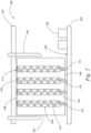
Figure 2 shows a cross-section through a power electronics assembly for an electric vehicle shown inFigure 1 ; -
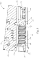
Figure 3 shows a perspective view of another power electronics assembly for an electric vehicle shown inFigure 1 ; and -
Figure 4 shows a perspective view of the electrically insulating housing of the power electronics assembly shown inFigure 3 . - In overview, the
electric motor system 10 ofFigure 1 comprisesmotor 2 and acontroller 20 to control operation of the motor. Theelectric motor system 10 also comprises acooling apparatus 4.Cooling apparatus 4 is coupled to both themotor 2 andcontroller 20 to remove heat produced by the operation of themotor 2 andcontroller 20. A drive output of the motor provides torque to drive a drive plate 8 coupled to a drive axle of a vehicle. Thecontroller 20 comprises apower electronics assembly 100 as shown for example inFigures 2 ,3 and4 . Although embodiments of the disclosure have particular usefulness in vehicles other uses are envisaged. -
Power electronics assembly 100 comprises afirst circuit board 101 and asecond circuit board 103. Thepower electronics assembly 100 is configured to maintain an electrical connection between thefirst circuit board 101 and thesecond circuit board 103 in the event that thesecond circuit board 103 moves relative to thefirst circuit board 101, for example due to movement, such as vibrations and/or thermal expansion of thesecond circuit board 103. - The
second circuit board 103 is spaced from thefirst circuit board 101 by a stand-off distance. For example the two boards may be arranged parallel to each other with a pre-determined stand-off spacing between them. As explained below with reference toFigure 2 , an electrically insulating housing is held between the first circuit board and the second circuit board. A number of channels pass through this housing and a conductor is arranged in each. The conductors are arranged to move resiliently along the channels - for example they may be resiliently deformable or coupled to a bias provider of some kind, such as a spring or any other biasing means. A restraint, such as a clip, holds the electrically insulating housing to the first circuit board and opposes the force on the electrically insulating housing caused by the biasing of these conductors. This enables the housing to be held in place on the first circuit board by the restraint, with the biased conductors in position. - A second circuit board can then be fixed to the first circuit board by a fixture such as a bolt. Arranging the second circuit board in this way presses the conductors toward the first circuit board and reduces the force on the electrically insulating housing caused by the biasing of the plurality of conductors.
- The
first circuit board 101 may comprise a composite material, for example a fiberglass material, for example it may be an FR4 board. Thesecond circuit board 103 may comprise an insulated metal substrate (IMS), for example an aluminium substrate insulated with a layer of a dielectric such as a polyamide, for example Kapton. In some examples, thesecond circuit board 103 is coupled to thecooling apparatus 4, for example by a heat sink. Interposed between thefirst circuit board 101 and thesecond circuit board 103 is electrically insulatinghousing 107. In some embodiments, thefirst circuit board 101 and thesecond circuit board 103 are mechanically coupled to each other. This mechanical coupling may fix a stand-off distance between the two circuit boards - for example the boards may be spaced apart and generally parallel with each other, and the electrically insulating housing may extend between the boards, in a direction transverse to the two boards. - As noted above, the electrically insulating
housing 107 comprises a plurality ofchannels 109, in the examples shown inFigures 2 ,3 and4 fourchannels 109, that extend from afirst side 106 of the electrically insulatinghousing 107 to asecond side 108 of the electrically insulatinghousing 107. Thechannels 109 each terminate in a correspondingfirst aperture 111 on thefirst side 106 of the electricallyinsulating housing 107 and in a correspondingsecond aperture 113 on thesecond side 108 of the electrically insulatinghousing 107. - In the examples shown in
Figures 2 ,3 and4 , each of the second plurality ofapertures 113 is narrower than each of the first plurality ofapertures 111. Thechannels 109 each have a longitudinal axis in a direction corresponding to a major dimension of each of thechannels 109. The longitudinal axis of each of thechannels 109 may be aligned with each corresponding first 111 and second 113 aperture. In the examples shown inFigures 2 ,3 and4 , thechannels 109 are aligned with each other in a direction transverse to the longitudinal axis of each of thechannels 109. - Although in the examples shown in
Figures 2 ,3 and4 , the first plurality ofapertures 111 and the second plurality of apertures 1 13 are opposing each other and aligned along the longitudinal axis of each of thechannels 109, theapertures channels 109. - The
channels 109 each further comprise aretaining member 119, which in the examples shown inFigures 2 ,3 and4 is a flange located at an end of each of thechannels 109. Theretaining member 119 of eachchannel 109 in these examples comprises a narrowing of eachchannel 109 towards thesecond side 108 of the electrically insulatinghousing 107 provided by the flange and resulting in eachsecond aperture 113 being narrower than eachfirst aperture 111. - The electrically insulating
housing 107 further comprises aclip 125 for detachably coupling the electrically insulatinghousing 107 to thefirst circuit board 101. In the examples shown inFigures 2 ,3 and4 , theclip 125 comprises two legs. Each leg may be located on an opposite side of the electrically insulatinghousing 107. The legs may be elongate and aligned with thechannels 109. The legs and the channels may also be aligned in a direction transverse to the longitudinal axis of each of thechannels 109. Each leg may be coupled to the electrically insulatinghousing 107 at its proximal end, and may be resilient so that the distal end of the leg can be deflected but will spring back. Each leg may comprise aflange 131 at its distal end, as shown inFigures 3 and4 . The flange may comprise a ramp portion so that the leg can be deflected by the ramp as the leg is pushed through an aperture, but then will spring back so that the flange captures the leg in the aperture. In this configuration, each leg extends beyond thefirst side 106 of the electrically insulatinghousing 107 by a distance greater than the thickness of thefirst circuit board 101, so that a portion of each leg comprising the flange extends beyond thefirst circuit board 101 when the electrically insulatinghousing 109 is coupled to thefirst circuit board 101. For example, the distance along each leg of theclip 125 between the flange to a point on the leg parallel to thefirst side 106 of the electrically insulatinghousing 107 may correspond to the thickness of thefirst circuit board 101. - The electrically insulating
housing 107 further comprises a rigid locator such as alocator pin 133, for example a pair oflocator pins 133.Such locator pins 133 may be arranged parallel to the longitudinal axis of each of thechannels 109, and in the examples shown inFigures 2 ,3 and4 , are arranged parallel to the longitudinal axis of the legs of theclip 125. Thelocator pins 133, according to the invention, are longer than theclip 125.. Thelocator pins 133 are coupled to the electrically insulatinghousing 107, and in the examples shown inFigures 2 ,3 and4 , the twolocator pins 133 are coupled to the electrically insulatinghousing 107 on opposing sides of the electrically insulatinghousing 107, and out of alignment with the legs of theclip 125 and out of alignment with a direction of alignment of thechannels 109, in a direction transverse to the longitudinal axis of thechannels 109. In the examples shown inFigures 2 ,3 and4 , onelocator pin 133 is coupled to the electrically insulatinghousing 107 between a first andsecond channel 109 to one side of the electrically insulatinghousing 107, and asecond locator pin 133 is coupled to the electrically insulatinghousing 107 between a third andfourth channel 109 to another side of the electrically insulatinghousing 107. - Each
channel 109 holds acorresponding bias provider 115 that provides a biasing force on a corresponding conductor of the assembly. Eachbias provider 115 may extend substantially the full length of eachcorresponding channel 109. In the examples shown inFigures 2 ,3 and4 , the bias provider 1 15 is a helical spring, but other biasing means may be used, for example a leaf spring, an electromechanical actuator, a rubber grommet, or a resilient member. In some examples, eachchannel 109 may hold a plurality ofbias providers 115, for example twobias providers 115 separated by a resilient member. In some examples, eachchannel 109 may hold a plurality of bias providers 1 15, wherein each bias provider 1 15 interacts with a corresponding retainingmember 119, such that eachchannel 109 holds a plurality of retainingmembers 119. - Each
bias provider 115 comprises a corresponding conductor that projects through a corresponding one of the first plurality ofapertures 111 and through a corresponding one of the second plurality ofapertures 113. - The
first circuit board 101 comprisescontacts 116. Thecontacts 116 of thefirst circuit board 101 may be aligned with each of the first plurality ofapertures 111 of the electrically insulatinghousing 107. There may be asmany contacts 116 on thefirst circuit board 101 as there arechannels 109. - The
second circuit board 103 also comprisescontacts 117. Thecontacts 117 of thesecond circuit board 103 may be aligned with each of the second plurality ofapertures 113 of the electrically insulatinghousing 107. There may be asmany contacts 117 on thesecond circuit board 103 as there arechannels 109. - The
contacts second apertures second apertures contacts 117 on thesecond circuit board 103 may be substantially the same size as, or may be smaller than, each of the second plurality ofapertures 113. Thecontacts 116 on thefirst circuit board 101 may be substantially the same size as, or may be smaller than, each of the first plurality ofapertures 111. - In the examples shown in
Figures 2 ,3 and4 , each conductor comprises apin 121 that fits in and projects through each of the corresponding second plurality ofapertures 113 to engage thecorresponding contact 117 on thesecond circuit board 103. For example, each conductor may comprise thepin 121 at an end that, in use, corresponds to thesecond side 108 of the electrically insulatinghousing 107 facing thesecond circuit board 103. Thepin 121 may be in a direction parallel to the bias direction and/or the longitudinal direction of eachchannel 109. - In some examples, however, each conductor may not comprise a pin. In some examples, each conductor may comprise a portion transverse to the bias direction and/or the longitudinal direction of each
channel 109. For example, each conductor may comprise a coil or helix structure that spirals or coils inwards from an outer diameter of the conductor to an inner diameter. - In some examples, both ends of each conductor may be the same. In some examples, both ends of each conductor may comprise, for example, a helix or coil of varying diameter. In some examples the conductor's coil diameter may vary over its length. For example, the coil diameter of the conductor may narrow towards an end so that each conductor passes through a corresponding narrowing of each channel.
- In the examples shown in
Figures 2 ,3 and4 , thechannels 109,apertures contacts channels 109, although as mentioned above, in other examples at least one of thechannels 109,apertures contacts channels 109. - In some examples, the coil diameter of the conductor and/or
bias provider 115 may change over a portion of its length. For example, the coil diameter of the conductor and/orbias provider 115 may increase towards an end so that the conductor and/orbias provider 115 forms an outward spiral. In some examples, the coil diameter of the conductor and/orbias provider 115 may decrease towards an end so that the conductor and/orbias provider 115 forms an inward spiral. - In the examples shown in
Figures 2 ,3 and4 , eachbias provider 115 comprises each corresponding conductor so that the helical spring is both thebias provider 115 and the conductor and is therefore aconductive bias provider 115. In the examples shown inFigures 2 ,3 and4 , the coil diameter of theconductive bias provider 115 is substantially constant over the length of thebias provider 115 along its longitudinal axis. However, the coil diameter of theconductive bias provider 115 may decrease over a portion of its length, for example near an end of theconductive bias provider 115 opposite to the end with thepin 121 and near thefirst side 106 of the electrically insulatinghousing 107. Theconductive bias provider 115 may therefore form an inward spiral at an end, or at both ends. In other examples, the coil diameter of theconductive bias provider 115 may increase over a portion of its length. - The
contacts 117 of thesecond circuit board 103 are electrically coupled to aninverter 150. The first 101 and/or second 103 circuit boards may comprise other functionality which may include, for example, microprocessors, power supplies, capacitors and inductors configured for control filtering and conditioning. For example, thefirst circuit board 101 of the power electronics assembly may comprise a timing chip for controlling operation of theinverter 150. - In some examples the
first circuit board 101 and thesecond circuit board 103 are mechanically and electrically coupled by a power contact. The power contact may couple theinverter 150 on thesecond circuit board 103 to an electrical circuit on thefirst circuit board 101 and may be configured to pass AC current from the first circuit board to the inverter on thesecond circuit board 103, and DC current from the inverter on thesecond circuit board 103 to the electrical circuit on thefirst circuit board 101. - The
controller 20 is configured to derive a three-phase alternating current (AC) supply for themotor 2 from a direct current (DC)power source 6, in this example a battery. Theinverter 150 is configured to perform inversion, filtering and conditioning processing on the DC output of thepower source 6 to provide the motor with the required AC power source. Theinverter 150 is operable to convert a DC input to a three-phase AC output for use by themotor 2. Any suitable form of inverter may be used. In a preferred example, an insulated gate bipolar transistor (IGBT) inverter is used. In some cases MOSFETs or other IGFETs may also be used. Preferred characteristics of the IGBT inverter include high efficiency and fast switching. - The
clip 125 in the examples shown inFigures 2 ,3 and4 is configured to detachably couple the electrically insulatinghousing 107 to thefirst circuit board 101. The legs of theclip 125 are adapted to be received by correspondingholes 129 in thefirst circuit board 101 such that theclip 125 can "snap-fit" with thefirst circuit board 101. - The
first circuit board 101 and thesecond circuit board 103 may be separated by a predetermined distance, for example to allow cooling of the first 101 and/or second 103 circuit boards. A dimension of the electrically insulatinghousing 107 may fit within the predetermined distance between thefirst circuit board 101 and thesecond circuit board 103. For example, the full length of eachchannel 109 may fit within the predetermined distance between thefirst circuit board 101 and thesecond circuit board 103. For example, the distance between thefirst side 106 and thesecond side 108 of the electrically insulatinghousing 107 may fit within the predetermined distance between thefirst circuit board 101 and thesecond circuit board 103. - The
channels 109 of the electrically insulatinghousing 107 are configured to receive and hold thebias provider 115. For example they may be cylindrical tunnels through an insulating body. Thebias provider 115 of eachchannel 109 is configured to fit within eachchannel 109. The retainingmember 119 of eachchannel 109 is configured to interact with thebias provider 115 to project a corresponding conductor through a corresponding one of the first plurality ofapertures 111 and project the conductor through a corresponding one of the second plurality ofapertures 113 to electrically couple thefirst circuit board 101 with thesecond circuit board 103. - A portion of the
clip 125 may be configured to move in a direction transverse to the longitudinal axis of eachchannel 109 when the electrically insulatinghousing 107 is coupled to thefirst circuit board 101. For example, the legs of theclip 125 may be configured to move in a direction transverse to the longitudinal axis of eachchannel 109 when the electrically insulatinghousing 107 is coupled to thefirst circuit board 101. In the examples shown inFigures 3 and4 , the flange on each leg of theclip 125 may comprise a ramp portion that is operable to bend the legs in a direction transverse to the longitudinal axis of each of thechannels 109 as the electrically insulatinghousing 107 is pushed onto thefirst circuit board 101 in a direction parallel with the longitudinal axis of each of thechannels 109. Theflange 131 on each leg may be configured to detachably secure the electrically insulatinghousing 107 to thefirst circuit board 101. The legs of theclip 125 may be operable to detach the electrically insulatinghousing 107 from thefirst circuit board 101 by squeezing the legs together in a direction transverse to the longitudinal axis of each of thechannels 109, for example so that the flange on each leg can pass through the corresponding hole 130 on thefirst circuit board 101. - The locator pins 133 are configured to guide the electrically insulating
housing 107 as it is detachably coupled to and pressed against thefirst circuit board 101. Because the locator pins 133 may be longer than the legs of theclip 125, the locator pins 133 may be configured to align with a corresponding hole in thefirst circuit board 101 so that as the electrically insulatinghousing 107 is pressed towards thefirst circuit board 101 in a direction parallel to the longitudinal axis of the legs of theclip 125 and thechannels 109, the legs of theclip 125 are already aligned with the correspondingholes 129 of the first circuit board, to prevent damage occurring to the legs of theclip 125. Because the locator pins 133 and the legs of theclip 125 may be aligned parallel to the longitudinal axis of each of thechannels 109, the electrically insulatinghousing 107 can be slid into position on thefirst circuit board 101. - The
bias provider 115 of eachchannel 109 is configured to operate in an extended configuration and in a compressed configuration. Thebias provider 115 of eachchannel 109 is configured to be in the extended configuration when the electrically insulatinghousing 107 is detached from thefirst circuit board 101 and in the compressed configuration when the electrically insulatinghousing 107 is coupled to thefirst circuit board 101. In the extended configuration, eachbias provider 115 may be configured to be longer than the length of each of thechannels 109 along their longitudinal axis. - The electrically insulating
housing 107 is configured to retain eachbias provider 115 in eachcorresponding channel 109 when coupled to thefirst circuit board 101. The electrically insulatinghousing 107 may be configured to retain eachbias provider 115 in eachcorresponding channel 109 in its compressed configuration. In the examples shown inFigures 2 ,3 and4 , the retainingmember 119 of eachchannel 109 is configured to interact with eachbias provider 115 to prevent thebias provider 115 from escaping through thechannel 109 beyond the retainingmember 119. The electrically insulatinghousing 107 may therefore be configured to retain thebias provider 115 between the retainingmember 119 and thefirst circuit board 101. - In some examples where the
bias provider 115 comprises a spring or similar structure, for example where eachbias provider 115 comprises each corresponding conductor, and where the coil diameter varies over its length, the retainingmember 119 may be configured to interact with thebias provider 115 at a point where a change in coil diameter occurs. For example, the retainingmember 119 may comprise a flange and/or a narrowing in the diameter of eachchannel 109, and the flange or narrowing in diameter of eachchannel 109 may interact with thebias provider 115 such that a portion of thebias provider 115 with a larger coil diameter is arranged to be trapped between thefirst circuit board 101 and the retainingmember 119, and a portion of thebias provider 115 with a smaller coil diameter is arranged to be between thesecond circuit board 103 and the retainingmember 119 in use. - The
bias provider 115 of eachchannel 109 is configured to press each corresponding conductor against acorresponding contact circuit boards bias provider 115 of eachchannel 109 is configured to press each corresponding conductor against a corresponding contact on at least one of thecircuit boards channel 109. In the examples shown inFigures 2 ,3 and4 , eachbias provider 115 is configured to press each corresponding conductor against acorresponding contact 116 on thefirst circuit board 101 and against acorresponding contact 117 on thesecond circuit board 103 to maintain an electrical connection between thefirst circuit board 101 and thesecond circuit board 103. In this way, thepower electronics assembly 100 is arranged to electrically couple thefirst circuit board 101, for example components of the power electronics, for example a timing chip, to theinverter 150 of thesecond circuit board 103. - The electrically insulating
housing 107 may further be configured to align each corresponding conductor of eachbias provider 115 with thecorresponding contact 116 on thefirst circuit board 101 and thecorresponding contact 117 on thesecond circuit board 103. - In some examples, a portion of each conductor is configured to project through a corresponding one of the second plurality of
apertures 113 to press against thecorresponding contact 117 on thesecond circuit board 103. In the examples shown inFigures 2 ,3 and4 , the portion of each conductor configured to project through a corresponding one of the second plurality ofapertures 113 is apin 121. In some examples, a portion of each conductor is configured to project through a corresponding one of the first plurality ofapertures 113 to press against thecorresponding contact 116 on thefirst circuit board 101. - The conductor may be configured to increase its surface area in contact with a
contact contact bias provider 115 is in a compressed configuration. For example, where each conductor comprises a portion transverse to the bias direction and/or the longitudinal direction of eachchannel 109, the portion transverse to the bias direction and/or longitudinal direction of eachchannel 109 is configured to increase the contact area between the conductor and acorresponding contact pad circuit boards - For example, where the
bias provider 115 comprises each conductor, and thebias provider 115 is a helical spring and the coil diameter of the helical spring decreases towards an end opposite to that of thepin 121, the decrease in coil diameter is configured to increase the surface area of the helical spring in contact with thecontact 116 when biased against thefirst circuit board 101. - The
first side 106 of the electrically insulatinghousing 107 may be adapted to abut and/or form a seal with thefirst circuit board 101 when coupled to thefirst circuit board 101. Thesecond side 108 of the electrically insulatinghousing 107 may be adapted to abut and/or form a seal with thesecond circuit board 103 when the electrically insulatinghousing 107 is coupled to thefirst circuit board 101 and thefirst circuit board 101 is coupled to thesecond circuit board 103. - The power electronics assembly may be manufactured by providing the
first circuit board 101, providing the electrically insulatinghousing 107 comprising the plurality ofchannels 109, inserting thecorresponding bias provider 115 through eachfirst aperture 111 into eachchannel 109 to engage each corresponding retainingmember 119, and coupling the electrically insulatinghousing 107 to thefirst circuit board 101 so that thefirst side 106 of the electrically insulatinghousing 107 faces thefirst circuit board 101, thereby trapping eachbias provider 105 within each correspondingchannel 109 of the electrically insulatinghousing 107 between each corresponding retainingmember 119 and thefirst circuit board 101. - The electrically insulating
housing 107, theclip 125 and the locator pins 133 may be integrally moulded, or for example, theclip 125 and/or the locator pins 133 may be coupled to the electrically insulatinghousing 107, for example by ultrasonic welding. The electrically insulatinghousing 107 may be made from a plastics material. - The
first circuit board 101 may further be mechanically coupled to thesecond circuit board 103, so that thesecond side 108 of the electrically insulatinghousing 107 faces thesecond circuit board 103, and each of the conductors electrically engages with acorresponding contact 117 on thesecond circuit board 103. - Coupling the electrically insulating
housing 107 to thefirst circuit board 101 comprises pressing the electrically insulatinghousing 107 against thefirst circuit board 101 in a direction parallel to the longitudinal axis of each of thechannels 109. It may first comprise aligning each of the locator pins 133 with a corresponding hole in thefirst circuit board 101 so that the legs of theclip 125 are also aligned with their correspondingholes 129 in thefirst circuit board 101. Eachchannel 109 and/or each bias provider 1 15 and/or corresponding conductor may also be aligned with the corresponding contacts 1 16 on thefirst circuit board 101. Coupling the electrically insulatinghousing 107 may further comprise sliding the locator pins 133 within their corresponding holes in thefirst circuit board 101, as the electrically insulatinghousing 107 is pressed against thefirst circuit board 101. - In the examples shown in
Figures 3 and4 , as the electrically insulatinghousing 107 is pressed against thefirst circuit board 101 in a direction parallel with the longitudinal axis of each of thechannels 109, the ramp portion of each of the legs of theclip 125 may interact with the correspondingholes 129 in the first circuit board to bend the legs in a direction transverse to the longitudinal axis of each of thechannels 109, for example so that the legs bend towards each other. Eachbias provider 115 within eachchannel 109 is then compressed from its extended configuration to its compressed configuration as it is squeezed between the retainingmember 119 and thefirst circuit board 101. Once the flange of each leg of theclip 125 passes over the first circuit board and past eachcorresponding hole 129, the legs snap into position so that the flange engages with thefirst circuit board 101 to detachably couple the electrically insulatinghousing 107 to thefirst circuit board 101, and retaining eachbias provider 115 in eachchannel 109 between the retainingmember 119 and thefirst circuit board 101 in its compressed configuration. - In operation, electrical signals from elements of the power electronics on the
first circuit board 101, for example from a timing chip, pass from thefirst circuit board 101 to thesecond circuit board 103, through each of the conductors of eachchannel 109 and the correspondingcontacts second circuit board 103, for example to control operation of theinverter 150. - The power electronics assembly is configured to maintain an electrical connection between the
first circuit board 101 and thesecond circuit board 103 in the event that thesecond circuit board 103 moves relative to thefirst circuit board 101 and/or the electrically insulatinghousing 107. Because thesecond circuit board 103 comprisesinverter 105, it may get hot in use and expand and/or move relative to thefirst circuit board 101 and/or the electrically insulatinghousing 107. Eachbias provider 115 and corresponding conductor is configured to accommodate this movement. - For example, if the
second circuit board 103 moves in a direction transverse to the longitudinal axis of each of thechannels 109, each corresponding conductor, for example eachpin 121, can slide over eachcorresponding contact 117 on thesecond circuit board 103 to accommodate this movement whilst still maintaining an electrical connection between thefirst circuit board 101 and thesecond circuit board 103. As another example, if thesecond circuit board 103 moves in a direction parallel to the longitudinal axis of each of thechannels 109, each corresponding conductor, for example eachpin 121, can project further out of each of the second plurality ofapertures 113, due to the bias ofbias provider 115, to maintain contact with eachcorresponding contact 117 on thesecond circuit board 103 to accommodate this movement whilst still maintaining an electrical connection between thefirst circuit board 101 and thesecond circuit board 103. - In an embodiment there is provided a power electronics assembly for an electric motor controller comprising:
- a first circuit board, a second circuit board and an electrically insulating housing coupled to the first circuit board, wherein the second circuit board comprises an insulated metal substrate, and the electrically insulating housing comprises:
- a plurality of channels, wherein each channel terminates in a first aperture on a first side of the electrically insulating housing and a second aperture on a second side of the electrically insulating housing;
- wherein each channel holds a bias provider, each bias provider configured to project a corresponding conductor through a corresponding one of the first plurality of apertures and through a corresponding one of the second plurality of apertures to electrically couple the first circuit board with the second circuit board;
- wherein each bias provider is configured to press each corresponding conductor against a corresponding contact on at least one of the circuit boards to maintain an electrical connection between the first circuit board and the second circuit board in the event that the second circuit board moves relative to the first circuit board and the electrically insulating housing.
- In such power electronics assemblies the electrically insulating housing may be detachably coupled to the first circuit board, for example the electrically insulating housing may comprise a clip for detachably coupling the electrically insulating housing to the first circuit board.
- In an embodiment there is also provided an electrical coupling for coupling a first circuit board to a second circuit board of an electric motor controller comprising an electrically insulating housing, the electrically insulating housing configured to detachably couple to the first circuit board, and wherein the electrically insulating housing comprises: a plurality of channels, wherein each channel terminates in a first aperture on a first side of the electrically insulating housing and a second aperture on a second side of the electrically insulating housing; a clip for detachably coupling the electrically insulating housing to the first circuit board; wherein each channel holds a bias provider and a retaining member, each bias provider configured to project a corresponding conductor through a corresponding one of the first plurality of apertures and through a corresponding one of the second plurality of apertures to electrically couple the first circuit board with the second circuit board; wherein each bias provider is configured to press each corresponding conductor against a corresponding contact on at least one of the circuit boards to maintain an electrical connection between the first circuit board and the second circuit board; and wherein the power electronics coupler is configured to retain each bias provider between each corresponding retaining member and the first circuit board when the electrically insulating housing is coupled to the first circuit board.
- A portion of the clip may be configured to move in a direction transverse to the longitudinal axis of each channel when the electrically insulating housing is detachably coupled to the first circuit board. The clip may comprise at least two legs, the legs each adapted to snap-fit with a corresponding hole in the first circuit board. The detachable coupling arrangement may comprise a locator pin for aligning the electrically insulating housing with the first circuit board. Each bias provider may be configured to press each corresponding conductor against a corresponding contact on at least one of the circuit boards along an axis corresponding to a longitudinal axis of each channel. Each bias provider may be configured to press each corresponding conductor against a corresponding contact on the first circuit board and against a corresponding contact on the second circuit board to maintain an electrical connection between the first circuit board and the second circuit board. Each bias provider may comprise the corresponding conductor. The electrically insulating housing's first side may be adapted to abut and form a seal with the first circuit board when coupled to the first circuit board. The electrically insulating housing's second side may be adapted to abut and form a seal with the second circuit board when the electrically insulating housing is coupled to the first circuit board and the first circuit board is coupled to the second circuit board. The electrically insulating housing may be configured to align each corresponding conductor with a corresponding electrically conductive pad on the first circuit board and a corresponding electrically conductive pad on the second circuit board. Each of the plurality of channels and corresponding first and second apertures may be equally spaced.
- Each of the channels of the electrically insulating housing may comprise a retaining member, and wherein each retaining member is configured to interact with each bias provider to project a corresponding conductor through a corresponding one of the first plurality of apertures and project the conductor through a corresponding one of the second plurality of apertures to electrically couple the first circuit board with the second circuit board. The electrically insulating housing may be configured to retain the bias provider between the retaining member and the first circuit board, for example the retaining member may comprise a flange at an end of each of the channels, for example the second plurality of apertures can be narrower than the first plurality of apertures. Each retaining member may comprise a narrowing of a corresponding one of the second plurality of apertures with respect to each of the corresponding first plurality of apertures. Each bias provider may extend the full length of each corresponding channel.
- It will be appreciated in the context of the present disclosure that the first circuit board may be mechanically coupled to the second circuit board and the two circuit boards may be separated by a predetermined distance. The electrically insulating housing may be configured to fit within the predetermined distance between the two circuit boards. The power electronics assembly may comprise a power contact, wherein the power contact couples an inverter on the second circuit board to an electrical circuit on the first circuit board and is configured to pass DC current from the inverter on the second circuit board to the electrical circuit on the first circuit board.
- It will be appreciated in the context of the present disclosure that the first circuit board of the power electronics assembly may comprise a timing chip, and the second circuit board of the power electronics assembly comprises a gate drive circuit and/or transistors for controlling the power electronics. In these embodiments the conductors of the electrically insulating housing may be arranged to electrically couple the timing chip of the first circuit board to the gate drive circuit and/or transistors of the second circuit board.
- The conductors may each comprise a pin, wherein each pin is configured to project through a corresponding one of the second plurality of apertures to press against a corresponding contact on at least one of the circuit boards.
- It will be appreciated in the context of the present disclosure that the first circuit board may comprises a composite material such as fiberglass, for example FR4. The second circuit board may comprise an insulated metal substrate, such as aluminium substrate. The substrate may be covered in an insulator such as polyamide, for example Kapton (RTM). A circuit may be printed over the insulator. The insulated metal substrate is coupled to a heat sink. For example it may be clamped to the heatsink, for example using one or more fittings which press it against the heat sink. A thermally conductive paste may be provided between the substrate and the heat sink.
- Embodiments of the disclosure also provide a method of manufacturing a power electronics assembly, the method comprising: providing a first circuit board; providing an electrically insulating housing, the housing comprising a plurality of channels, wherein each channel terminates in a first aperture on a first side of the electrically insulating housing and a second aperture on a second side of the electrically insulating housing and wherein each channel comprises a retaining member; inserting a corresponding bias provider through each first aperture into each channel to engage each corresponding retaining member, each bias provider configured to project a corresponding conductor through a corresponding one of the first plurality of apertures and through a corresponding one of the second plurality of apertures; coupling the electrically insulating housing to the first circuit board so that the first side faces the first circuit board, thereby trapping each bias provider within each corresponding channel of the electrically insulating housing between each corresponding retaining member and the first circuit board. Such methods may comprise mechanically coupling the first circuit board to a second circuit board, so that the second side of the electrically insulating housing faces the second circuit board, and each of the conductors electrically engages with a corresponding contact on the first circuit board and on the second circuit board to electrically couple the first circuit board to the second circuit board.
- The electrically insulating housing may comprise a clip, and coupling the electrically insulating housing to the first circuit board comprises pressing the electrically insulating housing against the first circuit board in a direction parallel to the longitudinal axis of each of the channels, and further comprises moving a portion of the clip in a direction transverse to the longitudinal axis of each of the channels as the electrically insulating housing is pressed against the first circuit board.
- Each of the plurality of conductors are arranged in a corresponding one of the plurality of channels and seated against a retaining member of said corresponding one of the plurality of channels. Each of the plurality of conductors are arranged to provide resilient movement of at least part of said conductor in a bias direction along the channel. The bias direction may correspond to the longitudinal axis of each of the channels.
- The electrically insulating housing comprises a rigid locator, for example a locator pin, and coupling the electrically insulating housing to the first circuit board may comprise aligning the locator pin with a corresponding hole on the first circuit board, and pressing the electrically insulating housing against the first circuit board so that the locator pin slides within the corresponding hole in the first circuit board.
- The rigid locator is adapted to oppose a force on the electrically insulating housing caused by an interaction between the restraint and the first circuit board to inhibit movement of the electrically insulating housing relative to the first circuit board. For example, in embodiments where the restraint comprises a flexible leg, when the restraint is coupled to the first circuit board it may exert a biasing force on the electrically insulating housing in a direction transverse to the bias direction of the conductors and/or in a direction transverse to the longitudinal axis of each of the channels, and the rigid locator may be adapted to oppose this biasing force to inhibit movement of the electrically insulating housing relative to the first circuit board.
- The restraint may be adapted to form an interference fit with a first circuit board. For example, the restraint may comprise a member adapted to fit with a corresponding part of the first circuit board. For example, the restraint may comprise a male member adapted to mate with a corresponding female member of the first circuit board.
- The restraint comprises a clip. For example, the restraint may comprise a snap-fit coupling. The snap-fit coupling may be a mechanical joint system where part-to-part attachment is accomplished with locating and locking features. The locating and locking features may be homogenous with one or other of the components being joined. Joining may involve one of the locking features moving aside for engagement with the mating part, followed by return of the locking feature toward its original position to latch the components together.
- In the context of the present disclosure other examples and variations of the apparatus and methods described herein will be apparent to a person of skill in the art.
Claims (12)
- An electrical coupling assembly for coupling a first circuit board (101) to a second circuit board (103) of an electric motor controller (20), the assembly comprising:an electrically insulating housing (107);a plurality of channels (109) through the electrically insulating housing (107), wherein each channel comprises an open end and a retaining member (119);a plurality of conductors (115) each arranged in a corresponding one of the plurality of channels (109) and seated against the retaining member of said corresponding one of the plurality of channels (109) and arranged to provide resilient movement of at least part of said conductor in a bias direction along the channel;a restraint (125, 131) adapted to secure the electrically insulating housing (107) to the first circuit board (101) thereby to close the open end of the channels (109) to trap the conductors between the retaining members and the first circuit board (101) and to bias the conductors into electrical contact with an electrical conductor of the first circuit board (101);characterized in thatthe restraint comprises at least one clip (125) having a flexible leg, andwherein the at least one leg is arranged to hold the electrically insulating housing (107) against the first circuit board (101) in opposition to the force applied to the electrically insulating housing (107) by the biasing of the plurality of conductors; andwherein the electrically insulating housing (107) comprises a rigid locator (133) adapted to align the electrically insulating housing (107) with a location on the first circuit board (101) prior to engagement of the restraint with the first circuit board (101) and to permit movement of the electrically insulating housing (107) in the bias direction;wherein the rigid locator comprises a locator pin that is longer than the flexible leg of the clip (125);wherein the at least one flexible leg is adapted to be deflected transverse to the bias direction relative to the rigid locator to allow the electrically insulating housing (107) to be locked in position at the selected location,wherein the rigid locator (133) is arranged to inhibit lateral movement of the electrically insulating housing (107) across the first circuit board (101), andwherein the rigid locator is adapted to oppose a force transverse to the bias direction on the electrically insulating housing (107) caused by interaction between the restraint (125, 131) and the first circuit board (101).
- The assembly of claim 1 wherein the restraint is adapted to one of:a) be at least partially deflected transverse to the bias direction; andb) mechanically secure the electrically insulating housing (107) to the first circuit board (101) via an interference fit.
- The assembly of claim 1 or 2 wherein each channel terminates in a first aperture on the first side of the electrically insulating housing (107) and a second aperture on a second side of the electrically insulating housing (107), and each conductor comprises a bias provider (115) configured to project the corresponding one of the conductors through a corresponding one of the first plurality of apertures and through a corresponding one of the second plurality of apertures for electrically coupling the first circuit board (101) with a second circuit board (103), for example wherein the assembly is configured to retain each bias provider (115) between each corresponding retaining member and the first circuit board when, in use, the electrically insulating housing (107) is coupled to the first circuit board (101) by the restraint, for example wherein each bias provider (115) is configured to press each corresponding conductor against a corresponding contact on at least one of the circuit boards to maintain an electrical connection between the first circuit board (101) and the second circuit board (103).
- The assembly of any preceding claim, wherein the at least one flexible leg comprises a flange adapted to lock the housing (107) to a circuit board, and a ramp adapted to deflect the at least one flexible leg, for example wherein the restraint comprises at least two legs, the legs each adapted to snap-fit with a corresponding hole in the first circuit board (101).
- The assembly of any preceding claim, further comprising the first circuit board (101) and the second circuit board (103); whereinthe second circuit board (103) is spaced from the first circuit board (101) by a stand-off distance;the electrically insulating housing (107) is held between the first circuit board (101) and the second circuit board (103);each of the plurality of conductors are arranged to provide a conduction path through a corresponding one of the plurality of channels;the restraint (125, 131) is adapted to hold the electrically insulating housing (107) to the first circuit board (101) against a force on the electrically insulating housing (107) caused by the biasing of the plurality of conductors; andthe second circuit board (103) is held to the first circuit board (101) by a fixture such that the second circuit board (103) presses the conductors to reduce the force on the electrically insulating housing (107) caused by the biasing of the plurality of conductors.
- The assembly (100) of claim 5 wherein the first circuit board (101) is arranged at a first side of the housing (107) to close the channels (109) thereby to hold the conductors in the channels (109).
- The assembly of any preceding claim, wherein the channels (109) are arranged to retain the conductors in the event that the second circuit board (103) is unfixed from the first circuit board (101).
- The assembly (100) of claim 3 or any claim dependent thereon, wherein the bias providers (115) are arranged to provide force in a bias direction transverse to the first circuit board (101), wherein the restraint is adapted to hold the electrically insulating housing (107) at a selected location on the first circuit board (101), for example comprising a rigid locator arranged to locate the electrically insulating housing (107) at the selected location and to allow movement of the electrically insulating housing (107) in the bias direction, for example wherein the flexible leg is resilient.
- The assembly of any of the previous claims wherein each conductor comprises a bias provider (115), such as a spring, configured to press each corresponding conductor against a corresponding contact on at least one of the circuit boards along an axis corresponding to a longitudinal axis of each channel.
- An electric motor controller (20) comprising an assembly according to any of the previous claims.
- A method of manufacturing a power electronics assembly, the method comprising:providing an electrically insulating housing (107) comprising a plurality of channels (109), wherein each channel comprises a retaining member;arranging a conductor (115) in each channel, wherein each a plurality of conductors is arranged to provide a conduction path through a corresponding one of the plurality of channels (109) and so that, in each channel, a bias provider (115) is seated against a retaining member and arranged to permit resilient movement of the each one of the plurality of conductors along the each channel;coupling the electrically insulating housing (107) to a first circuit board (101) to enclose the plurality of conductors in the plurality of channels (109) so that the bias providers (115) urge the conductors into electrical contact with the first circuit board(1 01) ;fixing a second circuit board (103) to the first circuit board (101) to bring the second circuit board (103) into electrical contact with the plurality conductors and to further urge the plurality of conductors into electrical contact with the first circuit board (101);wherein the electrically insulating housing (107) further comprises a rigid locator (133), and wherein coupling the electrically insulating housing (107) to the first circuit board (101) comprises aligning the rigid locator with a corresponding hole on the first circuit board (101), and pressing the electrically insulating housing (107) against the first circuit board (101) so that the rigid locator slides within the corresponding hole in the first circuit board (101);wherein coupling the electrically insulating housing (107) to the first circuit board (101) further comprises providing a restraint (125, 131) comprising a clip (125) having at least one flexible leg adapted to be deflected transverse to the bias direction relative to the rigid locator to allow the electrically insulating housing (107) to be locked in position at the selected location,wherein the rigid locator comprises a locator pin that is longer than the flexible leg of the clip (125);wherein the rigid locator is arranged to inhibit lateral movement of the electrically insulating housing (107) across the first circuit board (101), and the at least one flexible leg is arranged to hold the electrically insulating housing (107) against the first circuit board (101) in opposition to the force applied to the electrically insulating housing (107) by the biasing of the plurality of conductors; andwherein the rigid locator is adapted to oppose a force transverse to the bias direction on the electrically insulating housing (107) caused by interaction between the restraint and the first circuit board (101).
- The method of claim 11, wherein each channel terminates in a first aperture on a first side of the electrically insulating housing (107) and a second aperture on a second side of the electrically insulating housing (107), the method comprising inserting a conductors through each first aperture into each channel to engage each corresponding retaining member, and closing the first apertures with the first circuit board (101), for example wherein closing the first apertures comprises trapping the bias providers (115) within each corresponding channel of the electrically insulating housing (107) between each corresponding retaining member and the first circuit board (101), for example further comprising mechanically coupling the first circuit board to a second circuit board (103) using a fixture, such as a bolt, so that the second side of the electrically insulating housing (107) faces the second circuit board (103), and each of the conductors electrically engages with a corresponding contact on the first circuit board (101) and on the second circuit board (103) to electrically couple the first circuit (101) board to the second circuit board (103), and coupling the electrically insulating housing (107) to the first circuit board (101) comprises pressing the electrically insulating housing (107) against the first circuit board (101) in a direction parallel to the longitudinal axis of each of the channels (109), and further comprises moving a portion of the clip (125) in a direction transverse to the longitudinal axis of each of the channels (109) as the electrically insulating housing (107) is pressed against the first circuit board (101).
Applications Claiming Priority (2)
| Application Number | Priority Date | Filing Date | Title |
|---|---|---|---|
| GB1511729.4A GB2539964B (en) | 2015-07-03 | 2015-07-03 | Electronics assembly |
| PCT/GB2016/052017 WO2017006100A1 (en) | 2015-07-03 | 2016-07-04 | Electronics assembly |
Publications (2)
| Publication Number | Publication Date |
|---|---|
| EP3317924A1 EP3317924A1 (en) | 2018-05-09 |
| EP3317924B1 true EP3317924B1 (en) | 2023-03-22 |
Family
ID=54013482
Family Applications (1)
| Application Number | Title | Priority Date | Filing Date |
|---|---|---|---|
| EP16744833.1A Active EP3317924B1 (en) | 2015-07-03 | 2016-07-04 | Electrical coupling assembly |
Country Status (4)
| Country | Link |
|---|---|
| US (1) | US10749283B2 (en) |
| EP (1) | EP3317924B1 (en) |
| GB (1) | GB2539964B (en) |
| WO (1) | WO2017006100A1 (en) |
Families Citing this family (2)
| Publication number | Priority date | Publication date | Assignee | Title |
|---|---|---|---|---|
| CN107196124B (en) * | 2017-05-16 | 2019-01-29 | 安费诺硕民科技(深圳)有限公司 | A kind of water-proof connector assemble method |
| CN113873753A (en) * | 2021-08-23 | 2021-12-31 | 信丰达诚科技有限公司 | Plug-in type circuit board structure |
Citations (3)
| Publication number | Priority date | Publication date | Assignee | Title |
|---|---|---|---|---|
| US6866519B2 (en) * | 2003-07-10 | 2005-03-15 | Wei-Fang Fan | Adaptable resilient pin assembly for BGA based IC encapsulation |
| US7270550B1 (en) * | 2006-07-11 | 2007-09-18 | Cheng Uei Precision Industry Co., Ltd. | Board to board connector |
| EP1898497A2 (en) * | 2006-09-05 | 2008-03-12 | Itt Manufacturing Enterprises, Inc. | Connector and contacts for use in the connector |
Family Cites Families (19)
| Publication number | Priority date | Publication date | Assignee | Title |
|---|---|---|---|---|
| GB1384550A (en) * | 1971-12-01 | 1975-02-19 | Int Computers Ltd | Test probe apparatus for use in testing electrically conductive paths |
| US4029375A (en) * | 1976-06-14 | 1977-06-14 | Electronic Engineering Company Of California | Miniature electrical connector |
| US5308252A (en) * | 1992-12-24 | 1994-05-03 | The Whitaker Corporation | Interposer connector and contact element therefore |
| JPH0982431A (en) * | 1995-09-19 | 1997-03-28 | Whitaker Corp:The | Electric connector and manufacturing method thereof |
| KR100373152B1 (en) * | 1999-11-17 | 2003-02-25 | 가부시키가이샤 아드반테스트 | Ic socket and ic testing apparatus |
| US6663439B2 (en) * | 2001-03-02 | 2003-12-16 | Tyco Electronics Corporation | Electrical connector with spring biased contacts |
| SG104969A1 (en) * | 2002-05-24 | 2004-07-30 | Fci Asia Technology Pte Ltd | An electrical connector |
| US6844749B2 (en) * | 2002-07-18 | 2005-01-18 | Aries Electronics, Inc. | Integrated circuit test probe |
| US6814626B2 (en) * | 2002-10-21 | 2004-11-09 | L & K Precision Industry Co., Ltd. | Electrical connector for chargeable battery |
| JP3768183B2 (en) | 2002-10-28 | 2006-04-19 | 山一電機株式会社 | IC socket for narrow pitch IC package |
| US7074047B2 (en) * | 2003-11-05 | 2006-07-11 | Tensolite Company | Zero insertion force high frequency connector |
| US7134909B2 (en) * | 2004-07-28 | 2006-11-14 | Fujitsu Limited | Connector circuit board |
| KR100714599B1 (en) * | 2004-12-21 | 2007-05-07 | 삼성전기주식회사 | Built-in antenna assembly of wireless communication terminal |
| JP5334997B2 (en) * | 2008-01-17 | 2013-11-06 | アンフェノル・コーポレーション | Interposer assembly and method |
| US7878834B2 (en) * | 2008-04-17 | 2011-02-01 | Neil Sherman | Connector for mating a contact pin with a device |
| JP2011257227A (en) | 2010-06-08 | 2011-12-22 | Panasonic Corp | Semiconductor inspection device and inspection method |
| JP5655914B1 (en) | 2013-08-30 | 2015-01-21 | 第一精工株式会社 | Electrical connector housing, electrical connector, and connector terminal mounting method |
| JP6257253B2 (en) * | 2013-10-07 | 2018-01-10 | 日本航空電子工業株式会社 | connector |
| JP6108462B2 (en) * | 2013-10-18 | 2017-04-05 | 日本航空電子工業株式会社 | connector |
-
2015
- 2015-07-03 GB GB1511729.4A patent/GB2539964B/en active Active
-
2016
- 2016-07-04 EP EP16744833.1A patent/EP3317924B1/en active Active
- 2016-07-04 WO PCT/GB2016/052017 patent/WO2017006100A1/en not_active Ceased
- 2016-07-04 US US15/739,282 patent/US10749283B2/en not_active Expired - Fee Related
Patent Citations (3)
| Publication number | Priority date | Publication date | Assignee | Title |
|---|---|---|---|---|
| US6866519B2 (en) * | 2003-07-10 | 2005-03-15 | Wei-Fang Fan | Adaptable resilient pin assembly for BGA based IC encapsulation |
| US7270550B1 (en) * | 2006-07-11 | 2007-09-18 | Cheng Uei Precision Industry Co., Ltd. | Board to board connector |
| EP1898497A2 (en) * | 2006-09-05 | 2008-03-12 | Itt Manufacturing Enterprises, Inc. | Connector and contacts for use in the connector |
Also Published As
| Publication number | Publication date |
|---|---|
| US10749283B2 (en) | 2020-08-18 |
| US20180183164A1 (en) | 2018-06-28 |
| GB2539964A (en) | 2017-01-04 |
| EP3317924A1 (en) | 2018-05-09 |
| GB201511729D0 (en) | 2015-08-19 |
| GB2539964B (en) | 2018-07-18 |
| WO2017006100A1 (en) | 2017-01-12 |
Similar Documents
| Publication | Publication Date | Title |
|---|---|---|
| US10971914B2 (en) | Circuit assembly | |
| US10418737B2 (en) | Terminal connection component, and terminal connection structure between control unit using the same and motor | |
| EP2063683A1 (en) | Electric heater and its manufacturing method | |
| EP2475236A2 (en) | Power Switching Circuitry | |
| CN106489078B (en) | Probes and electronic devices using probes | |
| CN106537058B (en) | Control device for electric heating equipment and method for manufacturing such a control device | |
| US10749283B2 (en) | Electronics assembly for coupling two circuit boards | |
| CN106486439B (en) | Power electronics submodule including two-part housing | |
| CN111406447B (en) | Cooling and hold-down fixture for short lead power supply units | |
| US10985487B2 (en) | Electrical connector between a bus and a circuit breaker | |
| CN111164837A (en) | high current connector | |
| JP2022551235A (en) | Compressor drive device and mounting method of said device | |
| CN104285342B (en) | The system transmitted for electric current | |
| CN107004535B (en) | Vacuum switchgear, and contact assembly and method of securing electrical contacts to electrodes thereof | |
| EP3540754B1 (en) | Component group for galvanically separating an armature and a switching bridge of a relay, the switching bridge being arranged on a switching bridge carrier, and relay | |
| JP2012119542A (en) | Structure and method of fixing heat source element and thermal conductive member to each other | |
| CN117374629A (en) | Contact device, circuit board device, method for producing a circuit board device, and motor vehicle | |
| CN111225544A (en) | Heat sink for electronic component | |
| US20190208669A1 (en) | Cooling apparatus for an electrical component | |
| US20240098846A1 (en) | Control Device and Method of Manufacturing a Control Device | |
| JP2015231245A (en) | Bus bar, motor control device, and method of assembling motor control device | |
| US9655169B2 (en) | Electric heater | |
| US20250249770A1 (en) | Induction charging unit and energy transfer system with same | |
| CN113056965A (en) | Method for assembling an electrical apparatus and associated electrical apparatus | |
| EP3340757B1 (en) | Resistance-limited electrical interconnects |
Legal Events
| Date | Code | Title | Description |
|---|---|---|---|
| STAA | Information on the status of an ep patent application or granted ep patent |
Free format text: STATUS: THE INTERNATIONAL PUBLICATION HAS BEEN MADE |
|
| PUAI | Public reference made under article 153(3) epc to a published international application that has entered the european phase |
Free format text: ORIGINAL CODE: 0009012 |
|
| STAA | Information on the status of an ep patent application or granted ep patent |
Free format text: STATUS: REQUEST FOR EXAMINATION WAS MADE |
|
| 17P | Request for examination filed |
Effective date: 20180112 |
|
| AK | Designated contracting states |
Kind code of ref document: A1 Designated state(s): AL AT BE BG CH CY CZ DE DK EE ES FI FR GB GR HR HU IE IS IT LI LT LU LV MC MK MT NL NO PL PT RO RS SE SI SK SM TR |
|
| AX | Request for extension of the european patent |
Extension state: BA ME |
|
| DAV | Request for validation of the european patent (deleted) | ||
| DAX | Request for extension of the european patent (deleted) | ||
| STAA | Information on the status of an ep patent application or granted ep patent |
Free format text: STATUS: EXAMINATION IS IN PROGRESS |
|
| 17Q | First examination report despatched |
Effective date: 20190306 |
|
| RAP1 | Party data changed (applicant data changed or rights of an application transferred) |
Owner name: TURNTIDE DRIVES LIMITED |
|
| GRAP | Despatch of communication of intention to grant a patent |
Free format text: ORIGINAL CODE: EPIDOSNIGR1 |
|
| STAA | Information on the status of an ep patent application or granted ep patent |
Free format text: STATUS: GRANT OF PATENT IS INTENDED |
|
| RIC1 | Information provided on ipc code assigned before grant |
Ipc: H01R 12/52 20110101ALN20220330BHEP Ipc: H05K 1/02 20060101ALN20220330BHEP Ipc: H01R 12/58 20110101ALI20220330BHEP Ipc: H05K 1/14 20060101ALI20220330BHEP Ipc: H01R 107/00 20060101ALI20220330BHEP Ipc: H01R 12/70 20110101ALI20220330BHEP Ipc: H01R 13/24 20060101ALI20220330BHEP Ipc: H01R 12/71 20110101ALI20220330BHEP Ipc: H01R 12/73 20110101AFI20220330BHEP |
|
| RIC1 | Information provided on ipc code assigned before grant |
Ipc: H01R 12/52 20110101ALN20220406BHEP Ipc: H05K 1/02 20060101ALN20220406BHEP Ipc: H01R 12/58 20110101ALI20220406BHEP Ipc: H05K 1/14 20060101ALI20220406BHEP Ipc: H01R 107/00 20060101ALI20220406BHEP Ipc: H01R 12/70 20110101ALI20220406BHEP Ipc: H01R 13/24 20060101ALI20220406BHEP Ipc: H01R 12/71 20110101ALI20220406BHEP Ipc: H01R 12/73 20110101AFI20220406BHEP |
|
| INTG | Intention to grant announced |
Effective date: 20220502 |
|
| GRAJ | Information related to disapproval of communication of intention to grant by the applicant or resumption of examination proceedings by the epo deleted |
Free format text: ORIGINAL CODE: EPIDOSDIGR1 |
|
| STAA | Information on the status of an ep patent application or granted ep patent |
Free format text: STATUS: EXAMINATION IS IN PROGRESS |
|
| GRAP | Despatch of communication of intention to grant a patent |
Free format text: ORIGINAL CODE: EPIDOSNIGR1 |
|
| STAA | Information on the status of an ep patent application or granted ep patent |
Free format text: STATUS: GRANT OF PATENT IS INTENDED |
|
| INTC | Intention to grant announced (deleted) | ||
| RIC1 | Information provided on ipc code assigned before grant |
Ipc: H01R 12/52 20110101ALN20220914BHEP Ipc: H05K 1/02 20060101ALN20220914BHEP Ipc: H01R 12/58 20110101ALI20220914BHEP Ipc: H05K 1/14 20060101ALI20220914BHEP Ipc: H01R 107/00 20060101ALI20220914BHEP Ipc: H01R 12/70 20110101ALI20220914BHEP Ipc: H01R 13/24 20060101ALI20220914BHEP Ipc: H01R 12/71 20110101ALI20220914BHEP Ipc: H01R 12/73 20110101AFI20220914BHEP |
|
| INTG | Intention to grant announced |
Effective date: 20220929 |
|
| GRAS | Grant fee paid |
Free format text: ORIGINAL CODE: EPIDOSNIGR3 |
|
| GRAA | (expected) grant |
Free format text: ORIGINAL CODE: 0009210 |
|
| STAA | Information on the status of an ep patent application or granted ep patent |
Free format text: STATUS: THE PATENT HAS BEEN GRANTED |
|
| AK | Designated contracting states |
Kind code of ref document: B1 Designated state(s): AL AT BE BG CH CY CZ DE DK EE ES FI FR GB GR HR HU IE IS IT LI LT LU LV MC MK MT NL NO PL PT RO RS SE SI SK SM TR |
|
| REG | Reference to a national code |
Ref country code: GB Ref legal event code: FG4D |
|
| REG | Reference to a national code |
Ref country code: CH Ref legal event code: EP |
|
| REG | Reference to a national code |
Ref country code: DE Ref legal event code: R096 Ref document number: 602016078430 Country of ref document: DE |
|
| REG | Reference to a national code |
Ref country code: IE Ref legal event code: FG4D |
|
| REG | Reference to a national code |
Ref country code: AT Ref legal event code: REF Ref document number: 1555865 Country of ref document: AT Kind code of ref document: T Effective date: 20230415 |
|
| REG | Reference to a national code |
Ref country code: LT Ref legal event code: MG9D |
|
| REG | Reference to a national code |
Ref country code: NL Ref legal event code: MP Effective date: 20230322 |
|
| PG25 | Lapsed in a contracting state [announced via postgrant information from national office to epo] |
Ref country code: RS Free format text: LAPSE BECAUSE OF FAILURE TO SUBMIT A TRANSLATION OF THE DESCRIPTION OR TO PAY THE FEE WITHIN THE PRESCRIBED TIME-LIMIT Effective date: 20230322 Ref country code: NO Free format text: LAPSE BECAUSE OF FAILURE TO SUBMIT A TRANSLATION OF THE DESCRIPTION OR TO PAY THE FEE WITHIN THE PRESCRIBED TIME-LIMIT Effective date: 20230622 Ref country code: LV Free format text: LAPSE BECAUSE OF FAILURE TO SUBMIT A TRANSLATION OF THE DESCRIPTION OR TO PAY THE FEE WITHIN THE PRESCRIBED TIME-LIMIT Effective date: 20230322 Ref country code: LT Free format text: LAPSE BECAUSE OF FAILURE TO SUBMIT A TRANSLATION OF THE DESCRIPTION OR TO PAY THE FEE WITHIN THE PRESCRIBED TIME-LIMIT Effective date: 20230322 Ref country code: HR Free format text: LAPSE BECAUSE OF FAILURE TO SUBMIT A TRANSLATION OF THE DESCRIPTION OR TO PAY THE FEE WITHIN THE PRESCRIBED TIME-LIMIT Effective date: 20230322 |
|
| REG | Reference to a national code |
Ref country code: AT Ref legal event code: MK05 Ref document number: 1555865 Country of ref document: AT Kind code of ref document: T Effective date: 20230322 |
|
| PG25 | Lapsed in a contracting state [announced via postgrant information from national office to epo] |
Ref country code: SE Free format text: LAPSE BECAUSE OF FAILURE TO SUBMIT A TRANSLATION OF THE DESCRIPTION OR TO PAY THE FEE WITHIN THE PRESCRIBED TIME-LIMIT Effective date: 20230322 Ref country code: NL Free format text: LAPSE BECAUSE OF FAILURE TO SUBMIT A TRANSLATION OF THE DESCRIPTION OR TO PAY THE FEE WITHIN THE PRESCRIBED TIME-LIMIT Effective date: 20230322 Ref country code: GR Free format text: LAPSE BECAUSE OF FAILURE TO SUBMIT A TRANSLATION OF THE DESCRIPTION OR TO PAY THE FEE WITHIN THE PRESCRIBED TIME-LIMIT Effective date: 20230623 Ref country code: FI Free format text: LAPSE BECAUSE OF FAILURE TO SUBMIT A TRANSLATION OF THE DESCRIPTION OR TO PAY THE FEE WITHIN THE PRESCRIBED TIME-LIMIT Effective date: 20230322 |
|
| PG25 | Lapsed in a contracting state [announced via postgrant information from national office to epo] |
Ref country code: SM Free format text: LAPSE BECAUSE OF FAILURE TO SUBMIT A TRANSLATION OF THE DESCRIPTION OR TO PAY THE FEE WITHIN THE PRESCRIBED TIME-LIMIT Effective date: 20230322 Ref country code: RO Free format text: LAPSE BECAUSE OF FAILURE TO SUBMIT A TRANSLATION OF THE DESCRIPTION OR TO PAY THE FEE WITHIN THE PRESCRIBED TIME-LIMIT Effective date: 20230322 Ref country code: PT Free format text: LAPSE BECAUSE OF FAILURE TO SUBMIT A TRANSLATION OF THE DESCRIPTION OR TO PAY THE FEE WITHIN THE PRESCRIBED TIME-LIMIT Effective date: 20230724 Ref country code: ES Free format text: LAPSE BECAUSE OF FAILURE TO SUBMIT A TRANSLATION OF THE DESCRIPTION OR TO PAY THE FEE WITHIN THE PRESCRIBED TIME-LIMIT Effective date: 20230322 Ref country code: EE Free format text: LAPSE BECAUSE OF FAILURE TO SUBMIT A TRANSLATION OF THE DESCRIPTION OR TO PAY THE FEE WITHIN THE PRESCRIBED TIME-LIMIT Effective date: 20230322 Ref country code: AT Free format text: LAPSE BECAUSE OF FAILURE TO SUBMIT A TRANSLATION OF THE DESCRIPTION OR TO PAY THE FEE WITHIN THE PRESCRIBED TIME-LIMIT Effective date: 20230322 |
|
| PGFP | Annual fee paid to national office [announced via postgrant information from national office to epo] |
Ref country code: GB Payment date: 20230801 Year of fee payment: 8 |
|
| PG25 | Lapsed in a contracting state [announced via postgrant information from national office to epo] |
Ref country code: SK Free format text: LAPSE BECAUSE OF FAILURE TO SUBMIT A TRANSLATION OF THE DESCRIPTION OR TO PAY THE FEE WITHIN THE PRESCRIBED TIME-LIMIT Effective date: 20230322 Ref country code: PL Free format text: LAPSE BECAUSE OF FAILURE TO SUBMIT A TRANSLATION OF THE DESCRIPTION OR TO PAY THE FEE WITHIN THE PRESCRIBED TIME-LIMIT Effective date: 20230322 Ref country code: IS Free format text: LAPSE BECAUSE OF FAILURE TO SUBMIT A TRANSLATION OF THE DESCRIPTION OR TO PAY THE FEE WITHIN THE PRESCRIBED TIME-LIMIT Effective date: 20230722 |
|
| PGFP | Annual fee paid to national office [announced via postgrant information from national office to epo] |
Ref country code: FR Payment date: 20230727 Year of fee payment: 8 Ref country code: DE Payment date: 20230731 Year of fee payment: 8 |
|
| REG | Reference to a national code |
Ref country code: DE Ref legal event code: R097 Ref document number: 602016078430 Country of ref document: DE |
|
| PLBE | No opposition filed within time limit |
Free format text: ORIGINAL CODE: 0009261 |
|
| STAA | Information on the status of an ep patent application or granted ep patent |
Free format text: STATUS: NO OPPOSITION FILED WITHIN TIME LIMIT |
|
| PG25 | Lapsed in a contracting state [announced via postgrant information from national office to epo] |
Ref country code: SI Free format text: LAPSE BECAUSE OF FAILURE TO SUBMIT A TRANSLATION OF THE DESCRIPTION OR TO PAY THE FEE WITHIN THE PRESCRIBED TIME-LIMIT Effective date: 20230322 Ref country code: DK Free format text: LAPSE BECAUSE OF FAILURE TO SUBMIT A TRANSLATION OF THE DESCRIPTION OR TO PAY THE FEE WITHIN THE PRESCRIBED TIME-LIMIT Effective date: 20230322 Ref country code: CZ Free format text: LAPSE BECAUSE OF FAILURE TO SUBMIT A TRANSLATION OF THE DESCRIPTION OR TO PAY THE FEE WITHIN THE PRESCRIBED TIME-LIMIT Effective date: 20230322 |
|
| 26N | No opposition filed |
Effective date: 20240102 |
|
| PG25 | Lapsed in a contracting state [announced via postgrant information from national office to epo] |
Ref country code: MC Free format text: LAPSE BECAUSE OF FAILURE TO SUBMIT A TRANSLATION OF THE DESCRIPTION OR TO PAY THE FEE WITHIN THE PRESCRIBED TIME-LIMIT Effective date: 20230322 |
|
| PG25 | Lapsed in a contracting state [announced via postgrant information from national office to epo] |
Ref country code: MC Free format text: LAPSE BECAUSE OF FAILURE TO SUBMIT A TRANSLATION OF THE DESCRIPTION OR TO PAY THE FEE WITHIN THE PRESCRIBED TIME-LIMIT Effective date: 20230322 |
|
| REG | Reference to a national code |
Ref country code: CH Ref legal event code: PL |
|
| REG | Reference to a national code |
Ref country code: BE Ref legal event code: MM Effective date: 20230731 |
|
| PG25 | Lapsed in a contracting state [announced via postgrant information from national office to epo] |
Ref country code: LU Free format text: LAPSE BECAUSE OF NON-PAYMENT OF DUE FEES Effective date: 20230704 |
|
| PG25 | Lapsed in a contracting state [announced via postgrant information from national office to epo] |
Ref country code: LU Free format text: LAPSE BECAUSE OF NON-PAYMENT OF DUE FEES Effective date: 20230704 |
|
| REG | Reference to a national code |
Ref country code: IE Ref legal event code: MM4A |
|
| PG25 | Lapsed in a contracting state [announced via postgrant information from national office to epo] |
Ref country code: CH Free format text: LAPSE BECAUSE OF NON-PAYMENT OF DUE FEES Effective date: 20230731 |
|
| PG25 | Lapsed in a contracting state [announced via postgrant information from national office to epo] |
Ref country code: IT Free format text: LAPSE BECAUSE OF FAILURE TO SUBMIT A TRANSLATION OF THE DESCRIPTION OR TO PAY THE FEE WITHIN THE PRESCRIBED TIME-LIMIT Effective date: 20230322 Ref country code: BE Free format text: LAPSE BECAUSE OF NON-PAYMENT OF DUE FEES Effective date: 20230731 |
|
| PG25 | Lapsed in a contracting state [announced via postgrant information from national office to epo] |
Ref country code: IE Free format text: LAPSE BECAUSE OF NON-PAYMENT OF DUE FEES Effective date: 20230704 |
|
| PG25 | Lapsed in a contracting state [announced via postgrant information from national office to epo] |
Ref country code: IE Free format text: LAPSE BECAUSE OF NON-PAYMENT OF DUE FEES Effective date: 20230704 |
|
| PG25 | Lapsed in a contracting state [announced via postgrant information from national office to epo] |
Ref country code: BG Free format text: LAPSE BECAUSE OF FAILURE TO SUBMIT A TRANSLATION OF THE DESCRIPTION OR TO PAY THE FEE WITHIN THE PRESCRIBED TIME-LIMIT Effective date: 20230322 |
|
| PG25 | Lapsed in a contracting state [announced via postgrant information from national office to epo] |
Ref country code: BG Free format text: LAPSE BECAUSE OF FAILURE TO SUBMIT A TRANSLATION OF THE DESCRIPTION OR TO PAY THE FEE WITHIN THE PRESCRIBED TIME-LIMIT Effective date: 20230322 |
|
| REG | Reference to a national code |
Ref country code: DE Ref legal event code: R119 Ref document number: 602016078430 Country of ref document: DE |
|
| GBPC | Gb: european patent ceased through non-payment of renewal fee |
Effective date: 20240704 |
|
| PG25 | Lapsed in a contracting state [announced via postgrant information from national office to epo] |
Ref country code: DE Free format text: LAPSE BECAUSE OF NON-PAYMENT OF DUE FEES Effective date: 20250201 |
|
| PG25 | Lapsed in a contracting state [announced via postgrant information from national office to epo] |
Ref country code: FR Free format text: LAPSE BECAUSE OF NON-PAYMENT OF DUE FEES Effective date: 20240731 |
|
| PG25 | Lapsed in a contracting state [announced via postgrant information from national office to epo] |
Ref country code: GB Free format text: LAPSE BECAUSE OF NON-PAYMENT OF DUE FEES Effective date: 20240704 |
|
| PG25 | Lapsed in a contracting state [announced via postgrant information from national office to epo] |
Ref country code: CY Free format text: LAPSE BECAUSE OF FAILURE TO SUBMIT A TRANSLATION OF THE DESCRIPTION OR TO PAY THE FEE WITHIN THE PRESCRIBED TIME-LIMIT; INVALID AB INITIO Effective date: 20160704 |
|
| PG25 | Lapsed in a contracting state [announced via postgrant information from national office to epo] |
Ref country code: HU Free format text: LAPSE BECAUSE OF FAILURE TO SUBMIT A TRANSLATION OF THE DESCRIPTION OR TO PAY THE FEE WITHIN THE PRESCRIBED TIME-LIMIT; INVALID AB INITIO Effective date: 20160704 |
|
| PG25 | Lapsed in a contracting state [announced via postgrant information from national office to epo] |
Ref country code: TR Free format text: LAPSE BECAUSE OF FAILURE TO SUBMIT A TRANSLATION OF THE DESCRIPTION OR TO PAY THE FEE WITHIN THE PRESCRIBED TIME-LIMIT Effective date: 20230322 |