EP3316325A1 - Quantum dot light emitting diode and quantum dot display device including the same - Google Patents
Quantum dot light emitting diode and quantum dot display device including the same Download PDFInfo
- Publication number
- EP3316325A1 EP3316325A1 EP17198262.2A EP17198262A EP3316325A1 EP 3316325 A1 EP3316325 A1 EP 3316325A1 EP 17198262 A EP17198262 A EP 17198262A EP 3316325 A1 EP3316325 A1 EP 3316325A1
- Authority
- EP
- European Patent Office
- Prior art keywords
- quantum dot
- light emitting
- emitting diode
- electrode
- material layer
- Prior art date
- Legal status (The legal status is an assumption and is not a legal conclusion. Google has not performed a legal analysis and makes no representation as to the accuracy of the status listed.)
- Granted
Links
Images





Classifications
-
- H—ELECTRICITY
- H05—ELECTRIC TECHNIQUES NOT OTHERWISE PROVIDED FOR
- H05B—ELECTRIC HEATING; ELECTRIC LIGHT SOURCES NOT OTHERWISE PROVIDED FOR; CIRCUIT ARRANGEMENTS FOR ELECTRIC LIGHT SOURCES, IN GENERAL
- H05B33/00—Electroluminescent light sources
- H05B33/12—Light sources with substantially two-dimensional [2D] radiating surfaces
- H05B33/14—Light sources with substantially two-dimensional [2D] radiating surfaces characterised by the chemical or physical composition or the arrangement of the electroluminescent material, or by the simultaneous addition of the electroluminescent material in or onto the light source
-
- H—ELECTRICITY
- H10—SEMICONDUCTOR DEVICES; ELECTRIC SOLID-STATE DEVICES NOT OTHERWISE PROVIDED FOR
- H10K—ORGANIC ELECTRIC SOLID-STATE DEVICES
- H10K50/00—Organic light-emitting devices
- H10K50/10—OLEDs or polymer light-emitting diodes [PLED]
- H10K50/11—OLEDs or polymer light-emitting diodes [PLED] characterised by the electroluminescent [EL] layers
- H10K50/115—OLEDs or polymer light-emitting diodes [PLED] characterised by the electroluminescent [EL] layers comprising active inorganic nanostructures, e.g. luminescent quantum dots
-
- G—PHYSICS
- G02—OPTICS
- G02B—OPTICAL ELEMENTS, SYSTEMS OR APPARATUS
- G02B6/00—Light guides; Structural details of arrangements comprising light guides and other optical elements, e.g. couplings
- G02B6/0001—Light guides; Structural details of arrangements comprising light guides and other optical elements, e.g. couplings specially adapted for lighting devices or systems
- G02B6/0011—Light guides; Structural details of arrangements comprising light guides and other optical elements, e.g. couplings specially adapted for lighting devices or systems the light guides being planar or of plate-like form
- G02B6/0013—Means for improving the coupling-in of light from the light source into the light guide
- G02B6/0023—Means for improving the coupling-in of light from the light source into the light guide provided by one optical element, or plurality thereof, placed between the light guide and the light source, or around the light source
-
- G—PHYSICS
- G02—OPTICS
- G02F—OPTICAL DEVICES OR ARRANGEMENTS FOR THE CONTROL OF LIGHT BY MODIFICATION OF THE OPTICAL PROPERTIES OF THE MEDIA OF THE ELEMENTS INVOLVED THEREIN; NON-LINEAR OPTICS; FREQUENCY-CHANGING OF LIGHT; OPTICAL LOGIC ELEMENTS; OPTICAL ANALOGUE/DIGITAL CONVERTERS
- G02F1/00—Devices or arrangements for the control of the intensity, colour, phase, polarisation or direction of light arriving from an independent light source, e.g. switching, gating or modulating; Non-linear optics
- G02F1/01—Devices or arrangements for the control of the intensity, colour, phase, polarisation or direction of light arriving from an independent light source, e.g. switching, gating or modulating; Non-linear optics for the control of the intensity, phase, polarisation or colour
- G02F1/13—Devices or arrangements for the control of the intensity, colour, phase, polarisation or direction of light arriving from an independent light source, e.g. switching, gating or modulating; Non-linear optics for the control of the intensity, phase, polarisation or colour based on liquid crystals, e.g. single liquid crystal display cells
- G02F1/133—Constructional arrangements; Operation of liquid crystal cells; Circuit arrangements
- G02F1/1333—Constructional arrangements; Manufacturing methods
- G02F1/1335—Structural association of cells with optical devices, e.g. polarisers or reflectors
- G02F1/1336—Illuminating devices
-
- H—ELECTRICITY
- H10—SEMICONDUCTOR DEVICES; ELECTRIC SOLID-STATE DEVICES NOT OTHERWISE PROVIDED FOR
- H10H—INORGANIC LIGHT-EMITTING SEMICONDUCTOR DEVICES HAVING POTENTIAL BARRIERS
- H10H20/00—Individual inorganic light-emitting semiconductor devices having potential barriers, e.g. light-emitting diodes [LED]
- H10H20/80—Constructional details
- H10H20/81—Bodies
- H10H20/811—Bodies having quantum effect structures or superlattices, e.g. tunnel junctions
- H10H20/812—Bodies having quantum effect structures or superlattices, e.g. tunnel junctions within the light-emitting regions, e.g. having quantum confinement structures
-
- H—ELECTRICITY
- H10—SEMICONDUCTOR DEVICES; ELECTRIC SOLID-STATE DEVICES NOT OTHERWISE PROVIDED FOR
- H10K—ORGANIC ELECTRIC SOLID-STATE DEVICES
- H10K50/00—Organic light-emitting devices
- H10K50/10—OLEDs or polymer light-emitting diodes [PLED]
- H10K50/11—OLEDs or polymer light-emitting diodes [PLED] characterised by the electroluminescent [EL] layers
-
- H—ELECTRICITY
- H10—SEMICONDUCTOR DEVICES; ELECTRIC SOLID-STATE DEVICES NOT OTHERWISE PROVIDED FOR
- H10K—ORGANIC ELECTRIC SOLID-STATE DEVICES
- H10K50/00—Organic light-emitting devices
- H10K50/10—OLEDs or polymer light-emitting diodes [PLED]
- H10K50/14—Carrier transporting layers
- H10K50/15—Hole transporting layers
-
- H—ELECTRICITY
- H10—SEMICONDUCTOR DEVICES; ELECTRIC SOLID-STATE DEVICES NOT OTHERWISE PROVIDED FOR
- H10K—ORGANIC ELECTRIC SOLID-STATE DEVICES
- H10K50/00—Organic light-emitting devices
- H10K50/10—OLEDs or polymer light-emitting diodes [PLED]
- H10K50/14—Carrier transporting layers
- H10K50/16—Electron transporting layers
-
- H—ELECTRICITY
- H10—SEMICONDUCTOR DEVICES; ELECTRIC SOLID-STATE DEVICES NOT OTHERWISE PROVIDED FOR
- H10K—ORGANIC ELECTRIC SOLID-STATE DEVICES
- H10K59/00—Integrated devices, or assemblies of multiple devices, comprising at least one organic light-emitting element covered by group H10K50/00
- H10K59/10—OLED displays
- H10K59/12—Active-matrix OLED [AMOLED] displays
- H10K59/121—Active-matrix OLED [AMOLED] displays characterised by the geometry or disposition of pixel elements
- H10K59/1213—Active-matrix OLED [AMOLED] displays characterised by the geometry or disposition of pixel elements the pixel elements being TFTs
-
- H—ELECTRICITY
- H10—SEMICONDUCTOR DEVICES; ELECTRIC SOLID-STATE DEVICES NOT OTHERWISE PROVIDED FOR
- H10K—ORGANIC ELECTRIC SOLID-STATE DEVICES
- H10K59/00—Integrated devices, or assemblies of multiple devices, comprising at least one organic light-emitting element covered by group H10K50/00
- H10K59/10—OLED displays
- H10K59/12—Active-matrix OLED [AMOLED] displays
- H10K59/122—Pixel-defining structures or layers, e.g. banks
-
- H—ELECTRICITY
- H10—SEMICONDUCTOR DEVICES; ELECTRIC SOLID-STATE DEVICES NOT OTHERWISE PROVIDED FOR
- H10K—ORGANIC ELECTRIC SOLID-STATE DEVICES
- H10K71/00—Manufacture or treatment specially adapted for the organic devices covered by this subclass
- H10K71/10—Deposition of organic active material
- H10K71/12—Deposition of organic active material using liquid deposition, e.g. spin coating
- H10K71/13—Deposition of organic active material using liquid deposition, e.g. spin coating using printing techniques, e.g. ink-jet printing or screen printing
-
- H—ELECTRICITY
- H10—SEMICONDUCTOR DEVICES; ELECTRIC SOLID-STATE DEVICES NOT OTHERWISE PROVIDED FOR
- H10P—GENERIC PROCESSES OR APPARATUS FOR THE MANUFACTURE OR TREATMENT OF DEVICES COVERED BY CLASS H10
- H10P14/00—Formation of materials, e.g. in the shape of layers or pillars
- H10P14/20—Formation of materials, e.g. in the shape of layers or pillars of semiconductor materials
- H10P14/34—Deposited materials, e.g. layers
- H10P14/3451—Structure
- H10P14/3452—Microstructure
- H10P14/3462—Nanowires
-
- H—ELECTRICITY
- H10—SEMICONDUCTOR DEVICES; ELECTRIC SOLID-STATE DEVICES NOT OTHERWISE PROVIDED FOR
- H10K—ORGANIC ELECTRIC SOLID-STATE DEVICES
- H10K2101/00—Properties of the organic materials covered by group H10K85/00
- H10K2101/30—Highest occupied molecular orbital [HOMO], lowest unoccupied molecular orbital [LUMO] or Fermi energy values
-
- Y—GENERAL TAGGING OF NEW TECHNOLOGICAL DEVELOPMENTS; GENERAL TAGGING OF CROSS-SECTIONAL TECHNOLOGIES SPANNING OVER SEVERAL SECTIONS OF THE IPC; TECHNICAL SUBJECTS COVERED BY FORMER USPC CROSS-REFERENCE ART COLLECTIONS [XRACs] AND DIGESTS
- Y02—TECHNOLOGIES OR APPLICATIONS FOR MITIGATION OR ADAPTATION AGAINST CLIMATE CHANGE
- Y02E—REDUCTION OF GREENHOUSE GAS [GHG] EMISSIONS, RELATED TO ENERGY GENERATION, TRANSMISSION OR DISTRIBUTION
- Y02E10/00—Energy generation through renewable energy sources
- Y02E10/50—Photovoltaic [PV] energy
- Y02E10/549—Organic PV cells
Definitions
- the present disclosure relates to a quantum dot (QD) light emitting diode, and more particularly, to a QD light emitting diode having an excellent hole transporting property and a QD display device including the same.
- QD quantum dot
- a field of display devices that represent all sorts of electrical signals as visual images has been developed rapidly.
- a flat panel display device such as a liquid crystal display (LCD) device, a plasma display panel (PDP) device, a field emission display (FED) device, and an organic light emitting diode (OLED) device, has been introduced.
- LCD liquid crystal display
- PDP plasma display panel
- FED field emission display
- OLED organic light emitting diode
- QD quantum dots
- FIG. 1 is a schematic view illustrating the related art QD light emitting diode.
- the QD light emitting diode 10 includes a first electrode 20, a second electrode 80 facing the first electrode 20, a QD emitting material layer (EML) 50 disposed between the first and second electrodes 20 and 80, a hole injection layer (HIL) 30 and a hole transporting layer (HTL) 40 located between the first electrode 20 and the QD EML 50, and an electron transporting layer (ETL) 60 and an electron injection layer (EIL) 70 positioned between the QD EML 50 and the second electrode 80.
- EML QD emitting material layer
- HIL hole injection layer
- HTL hole transporting layer
- ETL electron transporting layer
- EIL electron injection layer
- the first electrode 20 serves as an anode
- the second electrode 80 serves a cathode
- the QD EML 50 includes a plurality of quantum dots.
- the hole from the first electrode 20 is transported into the QD EML 50 through the HIL 30 and the HTL 40, and the electron from the second electrode 80 is transported into the QD EML 50 through the EIL 70 and the ETL 60.
- the QD light emitting diode 10 Since the QD has high quantum yield, it is expected that the QD light emitting diode 10 also provides high emitting efficiency. However, the related art QD light emitting diode 10 does not provide the desired emitting efficiency.
- the present disclosure is directed to a QD light emitting diode and a QD display device including the same that substantially obviate one or more of the problems due to limitations and disadvantages of the prior art, and have other advantages.
- a QD light emitting diode and a QD display device in the present disclosure have an excellent hole transporting property.
- a QD light emitting diode and a QD display device in the present disclosure have excellent emitting efficiency.
- An aspect of the present disclosure is a quantum dot (QD) light emitting diode including first and second electrodes facing each other; a QD emitting material layer between the first and second electrodes; and a semiconducting member acting as a hole transporting path in the QD emitting material layer.
- QD quantum dot
- QD quantum dot
- a quantum dot (QD) display device having a light emitting diode including an anode and a cathode facing each other; a quantum dot emitting material layer between the anode and the cathode; and a hole transporting enhancing member in the quantum dot emitting material layer, wherein the hole transporting enhancing member has a conduction band level between about -6.5 and about -5.0 eV, and has a shape having an aspect ratio of at least 2.
- Various embodiments provide a quantum dot (QD) light emitting diode, comprising: first and second electrodes facing each other; a QD emitting material layer between the first and second electrodes; and a semiconducting member acting as a hole transporting path in the QD emitting material layer.
- QD quantum dot
- the QD light emitting diode further comprises: a hole transporting layer between the first electrode and the QD emitting material layer, wherein the semiconducting member has a first end contacting the hole transporting layer.
- the semiconducting member has a second end disposed within the QD emitting material layer.
- the first and second ends may be opposite ends of the semiconducting member.
- the semiconducting member has a conduction band level being smaller than a HOMO level of the hole transporting layer and being larger than a conduction band level of the QD emitting material layer.
- the QD light emitting diode further comprises: an electron transporting layer between the QD emitting material layer and the second electrode, wherein the second end of the semiconducting member is spaced apart from the electron transporting layer.
- one end of the semiconducting member has at least two paths.
- the semiconducting member is disposed to be inclined with respect to at least one of upper and lower surfaces of the QD emitting material layer.
- an upper surface of the QD emitting material layer has a first height from a lower surface of the QD emitting material layer
- the semiconducting member has a second height from the lower surface of the QD emitting material layer, and wherein the second height is smaller than the first height
- the semiconducting member has a shape having an aspect ratio equal to or greater than 2.
- the semiconducting member includes a plate shape.
- the semiconducting member has a protrusion pattern at a surface.
- the semiconducting member includes at least one of CdSe, CdS, ZnSe, AlAs, GaP and SiC.
- Various embodiments provide a quantum dot display device having a quantum dot light emitting diode according to one or more embodiments described herein, wherein the semiconducting member of the quantum dot light emitting diode has a conduction band level between about -6.5 eV and about -5.0 eV,
- a quantum dot (QD) display device having a light emitting diode, the diode comprising:an anode and a cathode facing each other; a quantum dot emitting material layer between the anode and the cathode; and a hole transporting enhancing member in the quantum dot emitting material layer, wherein the hole transporting enhancing member has a conduction band level between about -6.5 eV and about -5.0 eV.
- the hole transporting enhancing member has a shape having an aspect ratio of at least 2.
- the QD display device further comprises a hole transporting layer between the anode and the quantum dot emitting material layer.
- the hole transporting layer has a HOMO level greater than the conduction band level of the hole transporting enhancing member and the quantum dot emitting material layer has a conduction band level smaller than the conduction band level of the hole transporting enhancing member.
- an upper surface of the quantum dot emitting material layer has a first height from a lower surface of the quantum dot emitting material layer
- the hole transporting enhancing member has a second height from the lower surface of the quantum dot emitting material layer, and wherein the second height is smaller than the first height
- the hole transporting enhancing member has one end contacting the hole transporting layer.
- the hole transporting enhancing member has the other end disposed within the QD emitting material layer.
- the hole transporting enhancing member includes at least one of CdSe, CdS, ZnSe, AlAs, GaP and SiC.
- the hole transporting property is decreased because of an energy level difference between the ETL and QD EML.
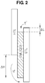
- FIG. 2 is an energy diagram of the related art QD light emitting diode. Since the energy level difference " ⁇ L" between the QD EML and the ETL is small, the electron “e-" is easily or efficiently transported from the ETL into the QD EML.
- the ligand at a surface of the QD serves as a barrier, the hole transporting problem in the related art QD light emitting diode is further serious. Namely, the hole transporting into the QDs in a lower region, which is close to the HTL, of the QD EML is relatively easy, but the hole transporting into the QDs in an upper region, which is far from the HTL, of the QD EML is very difficult.
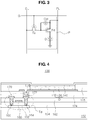
- FIG. 3 is a schematic circuit diagram of a QD display device according to the present disclosure.
- a gate line GL, a data line DL and a power line PL are formed, and a pixel region P is defined by the gate and data lines GL and DL.
- a switching thin film transistor (TFT) Ts, a driving TFT Td, a storage capacitor Cst and a QD light emitting diode D are formed.
- the switching TFT Ts is connected to the gate line GL and the data line DL, and the driving TFT Td and the storage capacitor Cst are connected to the switching TFT Ts and the power line PL.
- the QD light emitting diode D is connected to the driving TFT Td.
- the switching TFT Ts when the switching TFT Ts is turned on by a gate signal applied through the gate line GL, a data signal from the data line DL is applied to a gate electrode of the driving TFT Td and an electrode of the storage capacitor Cst through the switching TFT Ts.
- the driving TFT Td When the driving TFT Td is turned on by the data signal, an electric current is supplied to the QD light emitting diode D from the power line PL through the driving TFT Td. As a result, the QD light emitting diode D emits light.
- the storage capacitor Cst serves to maintain the voltage of the gate electrode of the driving TFT Td for one frame. Accordingly, the electroluminescent display device displays images.
- FIG. 4 is a schematic cross-sectional view of a QD display device according to the present disclosure.
- the QD display device 100 includes a substrate 150, the TFT Td on the substrate 150 and the QD light emitting diode D over the substrate 150 and connected to the TFT Td.
- the substrate 150 may be a glass substrate or a flexible substrate of a metal or a plastic.
- the substrate 150 may be a polyimide substrate.
- a buffer layer of an inorganic material e.g., silicon oxide or silicon nitride, may be formed on the substrate 150.
- the TFT Td is connected to the switching TFT Ts (shown in FIG. 3 ) and includes a semiconductor layer 152, a gate electrode 160, a source electrode 170 and a drain electrode 172.
- the semiconductor layer 152 is formed on the substrate 150.
- the semiconductor layer 152 may be formed of an oxide semiconductor material or poly-silicon.
- a light-shielding pattern (not shown) may be formed under the semiconductor layer 152. Accordingly, the light to the semiconductor layer 152 is shielded or blocked by the light-shielding pattern such that thermal degradation of the semiconductor layer 152 can be prevented.
- impurities may be doped into both sides of the semiconductor layer 152.
- a gate insulating layer 154 is formed on the semiconductor layer 152.
- the gate insulating layer 154 may be formed of an inorganic insulating material such as silicon oxide or silicon nitride.
- a gate electrode 160 which is formed of a conductive material, e.g., metal, is formed on the gate insulating layer 154 to correspond to a center portion of the semiconductor layer 152.
- the gate insulating layer 154 is formed on the entire surface of the substrate 150.
- the gate insulating layer 154 may be patterned to have the same shape as the gate electrode 160.
- An interlayer insulating layer 162 which is formed of an insulating material, is formed on the entire surface of the substrate 150 including the gate electrode 160.
- the interlayer insulating layer 162 may be formed of an inorganic insulating material, e.g., silicon oxide or silicon nitride, or an organic insulating material, e.g., benzocyclobutene or photo-acryl.
- the interlayer insulating layer 162 includes first and second contact holes 164 and 166 exposing both sides of the semiconductor layer 152.
- the first and second contact holes 164 and 166 are positioned at both sides of the gate electrode 160 to be spaced apart from the gate electrode 160.
- the first and second contact holes 164 and 166 extend into the gate insulating layer 154.
- the gate insulating layer 154 is patterned to have the same shape as the gate electrode 160, there may be no first and second contact holes 164 and 166 in the gate insulating layer 154.
- a source electrode 170 and a drain electrode 172 which are formed of a conductive material, e.g., metal, are formed on the interlayer insulating layer 162.
- the source electrode 170 and the drain electrode 172 are spaced apart from each other with respect to the gate electrode 160 and respectively contact both sides of the semiconductor layer 152 through the first and second contact holes 164 and 166.
- the source electrode 170 is connected to the power line PL (shown in FIG. 3 ).
- the TFT Td including the semiconductor layer 152, the gate electrode 160, the source electrode 170 and the drain electrode 172 serves as a driving element.
- the gate electrode 160, the source electrode 170 and the drain electrode 172 are positioned over the semiconductor layer 152. Namely, the TFT Td has a coplanar structure.
- the gate electrode may be positioned under the semiconductor layer, and the source and drain electrodes may be positioned over the semiconductor layer such that the TFT Td may have an inverted staggered structure.
- the semiconductor layer may be formed of amorphous silicon.
- the switching TFT Ts may have substantially the same structure as the TFT Td.
- a passivation layer 174 which includes a drain contact hole 176 exposing the drain electrode 172 of the TFT Td, is formed to cover the TFT Td.
- a first electrode 110 which is connected to the drain electrode 172 of the TFT Td through the drain contact hole 176, is separately formed on the passivation layer 174 in each pixel region.
- the first electrode 110 may be an anode and may be formed of a conductive material having a relatively high work function.
- the first electrode 110 may be formed of a transparent conductive material such as indium-tin-oxide (ITO) and indium-zinc-oxide (IZO).
- a reflection electrode or a reflection layer may be formed under the first electrode 110.
- the reflection electrode or the reflection layer may be formed of an aluminum-palladium-copper (APC) alloy.
- a bank layer 115 which covers edges of the first electrode 110, is formed on the passivation layer 174.
- the bank 115 exposes a center region of the first electrode 110 in the pixel region.
- An emitting layer 130 is formed on the first electrode 110.
- the emitting layer 130 will be explained in more detail.
- a second electrode 140 is formed on the emitting layer 130 over the substrate 150.
- the second electrode 140 is positioned at the entire surface of the display area.
- the second electrode 140 may be a cathode and may be formed of a conductive material having a relatively low work function.
- the second electrode 140 may be formed of one of aluminum (Al), magnesium (Mg) and an Al-Mg alloy.
- the first electrode 110, the emitting layer 130 and the second electrode 140 constitute the QD light emitting diode D.
- a QD EML in the emitting layer 130 may include a semiconductor rod such that a hole transporting property is improved. As a result, the emitting efficiency of the QD light emitting diode D and the QD display device 100 is also improved.
- FIG. 5 is a schematic cross-sectional view of a QD light emitting diode according to the present disclosure.
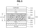
- the QD light emitting diode D includes the first electrode 110, the second electrode 140 facing the first electrode 110, a QD emitting material layer (EML) 230 between the first and second electrodes 110 and 140 and a semiconductor rod 240 (semiconducting member or hole transporting enhancing member) in the QD EML 230.
- the semiconductor rod 240 can be arranged to be inclined with respect to a surface (a lower surface or an upper surface) of the QD EML 230. Namely, the semiconductor rod 240 is not parallel or perpendicular to a surface of the QD EML 230.
- the first electrode 110 may be an anode
- the second electrode 140 may be a cathode.
- the QD EML 230 may include a plurality of QDs 232.
- the QD 232 may include a semiconductor material.
- the QD 232 may include a core at a center region and a shell covering the core. The light is emitted from the core.
- a ligand for dispersing the QD 232 in the solvent may be combined at a surface of the shell.
- the core and the shell have a difference in an energy ban gap.
- the QD 232 may be formed of a nano-size semiconductor material of II-VI group element or III-V group element.
- the nano-size semiconductor material may be one of CdSe, CdS, CdTe, ZnSe, ZnTe, ZnS, HgTe, InAs, InP and GaAs.
- the QD light emitting diode D may further include a hole transporting layer (HTL) 220 between the QD EML 230 and the first electrode 110.
- HTL hole transporting layer
- the upper surface of the QD EML 230 has a first height H1
- the semiconductor rod 240 has a second height H2 being smaller than the first height H1.
- the hole in the HTL 220 is directly transported into the QD EML 230 or is transported into the QD EML 230 through the semiconductor rod 240. Namely, the one end of the semiconductor rod 240 contacts the HTL 220 to serve as a hole transporting path. As a result, the hole is efficiently transported into a center region and an upper region of the QD EML 230 as well as the lower region of the QD EML 230.
- the semiconductor rod 240 has a conduction band being smaller than the highest occupied molecular orbital (HOMO) level of the HTL 220 and being larger than the conduction band (or the HOMO level) of the QD EML 230.
- the semiconductor rod 240 may include at least one of CdSe, CdS, ZnSe, AlAs, GaP and SiC.
- the conduction band of the semiconductor rod 240 is listed in Table 1.
- the semiconductor rod 240 has the conduction band level of about -6.5 to -5.0eV.
- FIG. 6 illustrates an energy diagram of a QD light emitting diode according to the present disclosure.
- the semiconductor rod 240 has a conduction band being smaller than the HOMO level of the HTL and being larger than the conduction band (or the HOMO level) of the QD EML. Since the hole "h+" is transported into the QD EML via a relatively small energy gap " ⁇ H1" between the HTL and the semiconductor rod 240 and a relatively small energy gap “ ⁇ H2" between the semiconductor rod 240 and the QD EML, the hole mobility is improved.
- the electron "e-" transporting from an electron transporting layer (ETL) into the QD EML is not blocked by the semiconductor rod 240. Accordingly, in the QD light emitting diode D, the charge balance is improved, and the emitting efficiency is increased.
- ETL electron transporting layer
- the semiconductor rod 240 has a major axis and a minor axis. Namely, the semiconductor rod 240 has an aspect ratio being greater than 1. Further, the aspect ratio of the semiconductor rod 240 can be greater than 2. For example, the aspect ratio of the semiconductor rod 240 may be about 2 to 10.
- the aspect ratio of the semiconductor rod 240 is too small, an area of the HTL 220 covered by the semiconductor rod 240 is increased.
- the other end of the semiconductor rod 240 is positioned in a center region of the QD EML 230. As a result, there is a limitation in the hole transporting into the QD 232 in the upper region of the QD EML 230.
- the QD light emitting diode D may further include the ETL 250 between the QD EML 230 and the second electrode 140.
- the semiconductor rod 240 may be spaced apart from the ETL 250.
- the one end of the semiconductor rod 240 contacts the HTL 220, and the other end of the semiconductor rod 240 is spaced apart from ETL 250.
- the semiconductor rod 240 contacts the ETL 250, the hole from the HTL 220 is transported into the ETL 250 through the semiconductor rod 240 such that the hole does not participate in the emission of the QD EML 230.
- the semiconductor rod 240 since the semiconductor rod 240 is spaced apart from the ETL 250, the emitting efficiency of the QD light emitting diode D is further increased.
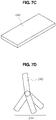
- FIGs. 7A to 7D illustrate various shapes of a semiconductor rod.
- the semiconductor rod 240 has a cylinder shape having a major axis and a minor axis.
- one end of the cylinder-shaped semiconductor rod 240 may contact the HTL 220 (shown in FIG. 5 ), and the other end of the cylinder-shaped semiconductor rod 240 may be spaced apart from the ETL 250 (shown in FIG. 5 ).
- the cross-section of the semiconductor rod 240 may have a rectangular (or square) shape such that the semiconductor rod 240 may have a rectangular (or square) pillar shape.
- the semiconductor rod 240 may include protrusion patterns 242 at the surface.
- the hole transporting property into the QD 232 (shown in FIG. 5 ) in the center region of the QD EML 230 is improved.
- a density of the protrusion patterns 242 in the center portion of the semiconductor rod 240 may be higher than that in the ends of the semiconductor rod 240.
- the semiconductor rod 240 may have a plate shape.
- one end of the semiconductor rod 240 may be branched such that at least two hole transporting paths may be provided at the one end of the semiconductor rod 240.
- the semiconductor rod 240 has a branched-end 244.
- the branched-end 244 may contact the HTL 220 (shown in FIG. 5 ) such that the hole transporting from the HTL 220 into the semiconductor rod 240 may be improved.
- the branched-end 244 may be positioned in the QD EML 230 (shown in FIG. 5 ) such that the hole transporting from the HTL 220 into the QD EML 230 is improved.
- the "rod" has a major axis and a minor axis
- the major axis of the semiconductor rod 240 is inclined to the surface of the HTL 220, and one end of the major axis of the semiconductor rod 240 is positioned in the QD EML 230.
- the QD light emitting diode D may further include a hole injection layer (HIL) 210 between the first electrode 110 and the HTL 220 and an electron injection layer (EIL) 260 between the second electrode 140 and the ETL 250.
- HIL hole injection layer
- EIL electron injection layer
- the HIL 210, the HTL 220, the QD EML 230, the semiconductor rod 240, the ETL 250 and the EIL 260 constitute the emitting layer 130.
- the HIL 210 may be formed of one of poly(3,4-ethylenedioxythiophene) polystyrene sulfonate (PEDOT:PSS), and the HTL 220 may include at least one of N,N'-diphenyl-N,N'-bis(3-methylphenyl)-1,1'biphenyl-4,4'diamine (TPD), poly(9-vinylcarbazole) (PVK), 4,4'-N, N'-dicarbazole-biphenyl (CBP), N,N'-bis(naphthalene-1-yl) -N,N'-bis(phenyl)benzidine ( ⁇ -NPD) and 4,4',4"-tris(N-carbazolyl)-triphenylamine (TCTA).
- PDOT:PSS poly(3,4-ethylenedioxythiophene) polystyrene sulfonate
- TPD N,N'-diphenyl-
- the ETL 250 may be formed of at least one of 2,2',2"-(1,3,5-benzinetriyl)-tris(1-phenyl-1-H-benzimidazole) (TPBi) and 3-(4-biphenylyl)-4-phenyl-5-t-butylphenyl-1,2,4-triazole (TAZ), and the EIL 260 may include LiF.
- TPBi 2,2',2"-(1,3,5-benzinetriyl)-tris(1-phenyl-1-H-benzimidazole)
- TEZ 3-(4-biphenylyl)-4-phenyl-5-t-butylphenyl-1,2,4-triazole
- LiF LiF
- the QD light emitting diode including the first electrode of ITO, the HIL of PEDOT:PSS, the HTL of p-TPD and PVK, the semiconductor rod of CdSe, the QD EML of InP QDs (red emission), the ETL of TPBi, the EIL of LiF and the second electrode of Al is manufactured.
- the emitting property of the QD light emitting diode is listed in Table 2 and shown in FIGs. 8A to 8C .
- Table 2 Turn On Max Volt (V) J (mA/cm 2 ) EQE Cd/m 2 Volt(V) J (mA/cm 2 ) EQE Cd/m 2 Ref 21 1.65 0.085 1.12 28 87.01 0.025 12.01 Ex 15 1.30 0.137 1.69 22 100.37 0.104 82.75
- the emitting property of the QD light emitting diode (Ex), which includes the semiconductor rod is substantially improved.
- the semiconductor rod does not participate in the emission (no color shift).
- the QD light emitting diode D includes the semiconductor rod 240, which is positioned in the QD EML 230 to serve as a hole transporting path, such that the charge balance in the QD light emitting diode D is improved.
- one end of the semiconductor rod 240 contacts the HTL 220, and the other end of the semiconductor rod 240 is positioned in the QD EML 230 to be spaced apart from the ETL 250.
- the hole transporting property into the QD EML 230 is uniformed and improved.
- the emitting efficiency of the QD light emitting diode D and the QD display device 100 is improved.
Landscapes
- Physics & Mathematics (AREA)
- Optics & Photonics (AREA)
- Engineering & Computer Science (AREA)
- Chemical & Material Sciences (AREA)
- Crystallography & Structural Chemistry (AREA)
- Nanotechnology (AREA)
- Inorganic Chemistry (AREA)
- Microelectronics & Electronic Packaging (AREA)
- General Physics & Mathematics (AREA)
- Nonlinear Science (AREA)
- Geometry (AREA)
- Mathematical Physics (AREA)
- Manufacturing & Machinery (AREA)
- Electroluminescent Light Sources (AREA)
- Led Devices (AREA)
Abstract
Description
- This application claims priority to and the benefit of Republic of Korea Patent Application No.
10-2016-0144575 - The present disclosure relates to a quantum dot (QD) light emitting diode, and more particularly, to a QD light emitting diode having an excellent hole transporting property and a QD display device including the same.
- Recently, as society has entered in earnest upon an information age, a field of display devices that represent all sorts of electrical signals as visual images has been developed rapidly. For example, a flat panel display device, such as a liquid crystal display (LCD) device, a plasma display panel (PDP) device, a field emission display (FED) device, and an organic light emitting diode (OLED) device, has been introduced.
- On the other hand, use of quantum dots (QD) to display devices has been researched or studied. In the QD, an electron in unstable state transitions from a conduction band to a valence band such that light is emitted. Since the QD has a high extinction coefficient and excellent quantum yield, strong fluorescent light is emitted from the QD. In addition, since the wavelength of the light from the QD is controlled by a size of the QD, entire visible light can be emitted by controlling the size of the QD.
-
FIG. 1 is a schematic view illustrating the related art QD light emitting diode. - As shown in
FIG. 1 , the QDlight emitting diode 10 includes afirst electrode 20, asecond electrode 80 facing thefirst electrode 20, a QD emitting material layer (EML) 50 disposed between the first andsecond electrodes first electrode 20 and theQD EML 50, and an electron transporting layer (ETL) 60 and an electron injection layer (EIL) 70 positioned between theQD EML 50 and thesecond electrode 80. - For example, the
first electrode 20 serves as an anode, and thesecond electrode 80 serves a cathode. - The QD EML 50 includes a plurality of quantum dots.
- In the QD
light emitting diode 10, the hole from thefirst electrode 20 is transported into theQD EML 50 through theHIL 30 and theHTL 40, and the electron from thesecond electrode 80 is transported into theQD EML 50 through theEIL 70 and theETL 60. - Since the QD has high quantum yield, it is expected that the QD
light emitting diode 10 also provides high emitting efficiency. However, the related art QDlight emitting diode 10 does not provide the desired emitting efficiency. - Accordingly, the present disclosure is directed to a QD light emitting diode and a QD display device including the same that substantially obviate one or more of the problems due to limitations and disadvantages of the prior art, and have other advantages.
- A QD light emitting diode and a QD display device in the present disclosure have an excellent hole transporting property.
- A QD light emitting diode and a QD display device in the present disclosure have excellent emitting efficiency.
- Additional features and advantages of the disclosure will be set forth in the description which follows, and in part will be apparent from the description, or may be learned by practice of the disclosure. The objectives and other advantages of the disclosure will be realized and attained by the structure particularly pointed out in the written description and claims hereof as well as the appended drawings.
- An aspect of the present disclosure is a quantum dot (QD) light emitting diode including first and second electrodes facing each other; a QD emitting material layer between the first and second electrodes; and a semiconducting member acting as a hole transporting path in the QD emitting material layer.
- Another aspect of the present disclosure is a quantum dot (QD) display device having a light emitting diode including an anode and a cathode facing each other; a quantum dot emitting material layer between the anode and the cathode; and a hole transporting enhancing member in the quantum dot emitting material layer, wherein the hole transporting enhancing member has a conduction band level between about -6.5 and about -5.0 eV, and has a shape having an aspect ratio of at least 2.
- Various embodiments provide a quantum dot (QD) light emitting diode, comprising: first and second electrodes facing each other; a QD emitting material layer between the first and second electrodes; and a semiconducting member acting as a hole transporting path in the QD emitting material layer.
- In one or more embodiments, the QD light emitting diode further comprises: a hole transporting layer between the first electrode and the QD emitting material layer, wherein the semiconducting member has a first end contacting the hole transporting layer.
- In one or more embodiments, the semiconducting member has a second end disposed within the QD emitting material layer. The first and second ends may be opposite ends of the semiconducting member.
- In one or more embodiments, the semiconducting member has a conduction band level being smaller than a HOMO level of the hole transporting layer and being larger than a conduction band level of the QD emitting material layer.
- In one or more embodiments, the QD light emitting diode further comprises: an electron transporting layer between the QD emitting material layer and the second electrode, wherein the the second end of the semiconducting member is spaced apart from the electron transporting layer.
- In one or more embodiments, one end of the semiconducting member has at least two paths.
- In one or more embodiments, the semiconducting member is disposed to be inclined with respect to at least one of upper and lower surfaces of the QD emitting material layer.
- In one or more embodiments, an upper surface of the QD emitting material layer has a first height from a lower surface of the QD emitting material layer, and the semiconducting member has a second height from the lower surface of the QD emitting material layer, and wherein the second height is smaller than the first height.
- In one or more embodiments, the semiconducting member has a shape having an aspect ratio equal to or greater than 2.
- In one or more embodiments, the semiconducting member includes a plate shape.
- In one or more embodiments, the semiconducting member has a protrusion pattern at a surface.
- In one or more embodiments, the semiconducting member includes at least one of CdSe, CdS, ZnSe, AlAs, GaP and SiC.
- Various embodiments provide a quantum dot display device having a quantum dot light emitting diode according to one or more embodiments described herein, wherein the semiconducting member of the quantum dot light emitting diode has a conduction band level between about -6.5 eV and about -5.0 eV,
- Various embodiments provide a quantum dot (QD) display device having a light emitting diode, the diode comprising:an anode and a cathode facing each other; a quantum dot emitting material layer between the anode and the cathode; and a hole transporting enhancing member in the quantum dot emitting material layer, wherein the hole transporting enhancing member has a conduction band level between about -6.5 eV and about -5.0 eV.
- In one or more embodiments, the hole transporting enhancing member has a shape having an aspect ratio of at least 2.
- In one or more embodiments, the QD display device further comprises a hole transporting layer between the anode and the quantum dot emitting material layer.
- In one or more embodiments, the hole transporting layer has a HOMO level greater than the conduction band level of the hole transporting enhancing member and the quantum dot emitting material layer has a conduction band level smaller than the conduction band level of the hole transporting enhancing member.
- In one or more embodiments, an upper surface of the quantum dot emitting material layer has a first height from a lower surface of the quantum dot emitting material layer, and the hole transporting enhancing member has a second height from the lower surface of the quantum dot emitting material layer, and wherein the second height is smaller than the first height.
- In one or more embodiments, the hole transporting enhancing member has one end contacting the hole transporting layer.
- In one or more embodiments, the hole transporting enhancing member has the other end disposed within the QD emitting material layer.
- In one or more embodiments, the hole transporting enhancing member includes at least one of CdSe, CdS, ZnSe, AlAs, GaP and SiC.
- It is to be understood that both the foregoing general description and the following detailed description are examples and are explanatory and are intended to provide further explanation of the disclosure as claimed.
- The accompanying drawings, which are included to provide a further understanding of the disclosure and are incorporated in and constitute a part of this application, illustrate aspects of the disclosure and together with the description serve to explain the principles of the disclosure.
- In the drawings:
-
FIG. 1 is a schematic view illustrating the related art QD light emitting diode; -
FIG. 2 is an energy diagram of the related art QD light emitting diode; -
FIG. 3 is a schematic circuit diagram of a QD display device according to the present disclosure; -
FIG. 4 is a schematic cross-sectional view of a QD display device according to the present disclosure; -
FIG. 5 is a schematic cross-sectional view of a QD light emitting diode according to the present disclosure; -
FIG. 6 is an energy diagram of a QD light emitting diode according to the present disclosure; -
FIGs. 7A to 7D illustrate various shapes of a semiconductor rod; and -
FIGs. 8A to 8C are graphs showing emitting properties of a QD light emitting diode according to the present disclosure. - Reference will now be made in detail to aspects of the disclosure, examples of which are illustrated in the accompanying drawings.
- In the related art QD light emitting diode, the hole transporting property is decreased because of an energy level difference between the ETL and QD EML.
- Namely, referring to
FIG. 2 , which is an energy diagram of the related art QD light emitting diode. Since the energy level difference "Δ L" between the QD EML and the ETL is small, the electron "e-" is easily or efficiently transported from the ETL into the QD EML. - However, since the energy level difference "Δ H" between the QD EML and the HTL is large, there is a limitation in the hole "h+" transporting from the HTL into the QD EML.
- In addition, the ligand at a surface of the QD serves as a barrier, the hole transporting problem in the related art QD light emitting diode is further serious. Namely, the hole transporting into the QDs in a lower region, which is close to the HTL, of the QD EML is relatively easy, but the hole transporting into the QDs in an upper region, which is far from the HTL, of the QD EML is very difficult.
- Accordingly, in the related art QD light emitting diode, a charge balance is lost, and the emitting efficiency is decreased.
-
FIG. 3 is a schematic circuit diagram of a QD display device according to the present disclosure. - As shown in
FIG. 3 , in the QD display device, a gate line GL, a data line DL and a power line PL are formed, and a pixel region P is defined by the gate and data lines GL and DL. In the pixel region P, a switching thin film transistor (TFT) Ts, a driving TFT Td, a storage capacitor Cst and a QD light emitting diode D are formed. - The switching TFT Ts is connected to the gate line GL and the data line DL, and the driving TFT Td and the storage capacitor Cst are connected to the switching TFT Ts and the power line PL. The QD light emitting diode D is connected to the driving TFT Td.
- In the QD display device, when the switching TFT Ts is turned on by a gate signal applied through the gate line GL, a data signal from the data line DL is applied to a gate electrode of the driving TFT Td and an electrode of the storage capacitor Cst through the switching TFT Ts.
- When the driving TFT Td is turned on by the data signal, an electric current is supplied to the QD light emitting diode D from the power line PL through the driving TFT Td. As a result, the QD light emitting diode D emits light. The storage capacitor Cst serves to maintain the voltage of the gate electrode of the driving TFT Td for one frame. Accordingly, the electroluminescent display device displays images.
-
FIG. 4 is a schematic cross-sectional view of a QD display device according to the present disclosure. - As shown in
FIG. 4 , theQD display device 100 includes asubstrate 150, the TFT Td on thesubstrate 150 and the QD light emitting diode D over thesubstrate 150 and connected to the TFT Td. - The
substrate 150 may be a glass substrate or a flexible substrate of a metal or a plastic. For example, thesubstrate 150 may be a polyimide substrate. - Although not shown, a buffer layer of an inorganic material, e.g., silicon oxide or silicon nitride, may be formed on the
substrate 150. - The TFT Td is connected to the switching TFT Ts (shown in
FIG. 3 ) and includes asemiconductor layer 152, agate electrode 160, asource electrode 170 and adrain electrode 172. - The
semiconductor layer 152 is formed on thesubstrate 150. Thesemiconductor layer 152 may be formed of an oxide semiconductor material or poly-silicon. - When the
semiconductor layer 152 is formed of the oxide semiconductor material, a light-shielding pattern (not shown) may be formed under thesemiconductor layer 152. Accordingly, the light to thesemiconductor layer 152 is shielded or blocked by the light-shielding pattern such that thermal degradation of thesemiconductor layer 152 can be prevented. On the other hand, when thesemiconductor layer 152 is formed of the polycrystalline silicon, impurities may be doped into both sides of thesemiconductor layer 152. - A
gate insulating layer 154 is formed on thesemiconductor layer 152. Thegate insulating layer 154 may be formed of an inorganic insulating material such as silicon oxide or silicon nitride. - A
gate electrode 160, which is formed of a conductive material, e.g., metal, is formed on thegate insulating layer 154 to correspond to a center portion of thesemiconductor layer 152. - In
FIG. 4 , thegate insulating layer 154 is formed on the entire surface of thesubstrate 150. Alternatively, thegate insulating layer 154 may be patterned to have the same shape as thegate electrode 160. - An interlayer insulating
layer 162, which is formed of an insulating material, is formed on the entire surface of thesubstrate 150 including thegate electrode 160. The interlayer insulatinglayer 162 may be formed of an inorganic insulating material, e.g., silicon oxide or silicon nitride, or an organic insulating material, e.g., benzocyclobutene or photo-acryl. - The interlayer insulating
layer 162 includes first and second contact holes 164 and 166 exposing both sides of thesemiconductor layer 152. The first and second contact holes 164 and 166 are positioned at both sides of thegate electrode 160 to be spaced apart from thegate electrode 160. - In
FIG. 4 , the first and second contact holes 164 and 166 extend into thegate insulating layer 154. Alternatively, when thegate insulating layer 154 is patterned to have the same shape as thegate electrode 160, there may be no first and second contact holes 164 and 166 in thegate insulating layer 154. - A
source electrode 170 and adrain electrode 172, which are formed of a conductive material, e.g., metal, are formed on theinterlayer insulating layer 162. Thesource electrode 170 and thedrain electrode 172 are spaced apart from each other with respect to thegate electrode 160 and respectively contact both sides of thesemiconductor layer 152 through the first and second contact holes 164 and 166. Thesource electrode 170 is connected to the power line PL (shown inFIG. 3 ). - The TFT Td including the
semiconductor layer 152, thegate electrode 160, thesource electrode 170 and thedrain electrode 172 serves as a driving element. - The
gate electrode 160, thesource electrode 170 and thedrain electrode 172 are positioned over thesemiconductor layer 152. Namely, the TFT Td has a coplanar structure. - Alternatively, in the TFT Td, the gate electrode may be positioned under the semiconductor layer, and the source and drain electrodes may be positioned over the semiconductor layer such that the TFT Td may have an inverted staggered structure. In this instance, the semiconductor layer may be formed of amorphous silicon.
- On the other hand, the switching TFT Ts (shown in
FIG. 3 ) may have substantially the same structure as the TFT Td. - A
passivation layer 174, which includes adrain contact hole 176 exposing thedrain electrode 172 of the TFT Td, is formed to cover the TFT Td. - A
first electrode 110, which is connected to thedrain electrode 172 of the TFT Td through thedrain contact hole 176, is separately formed on thepassivation layer 174 in each pixel region. Thefirst electrode 110 may be an anode and may be formed of a conductive material having a relatively high work function. For example, thefirst electrode 110 may be formed of a transparent conductive material such as indium-tin-oxide (ITO) and indium-zinc-oxide (IZO). - When the
QD display device 100 of the present disclosure is a top-emission type, a reflection electrode or a reflection layer may be formed under thefirst electrode 110. For example, the reflection electrode or the reflection layer may be formed of an aluminum-palladium-copper (APC) alloy. - A
bank layer 115, which covers edges of thefirst electrode 110, is formed on thepassivation layer 174. Thebank 115 exposes a center region of thefirst electrode 110 in the pixel region. - An emitting
layer 130 is formed on thefirst electrode 110. The emittinglayer 130 will be explained in more detail. - A
second electrode 140 is formed on the emittinglayer 130 over thesubstrate 150. Thesecond electrode 140 is positioned at the entire surface of the display area. Thesecond electrode 140 may be a cathode and may be formed of a conductive material having a relatively low work function. For example, thesecond electrode 140 may be formed of one of aluminum (Al), magnesium (Mg) and an Al-Mg alloy. - The
first electrode 110, the emittinglayer 130 and thesecond electrode 140 constitute the QD light emitting diode D. - In the QD light emitting diode D of the present disclosure, a QD EML in the emitting
layer 130 may include a semiconductor rod such that a hole transporting property is improved. As a result, the emitting efficiency of the QD light emitting diode D and theQD display device 100 is also improved. -
FIG. 5 is a schematic cross-sectional view of a QD light emitting diode according to the present disclosure. - As shown in
FIG. 5 , the QD light emitting diode D includes thefirst electrode 110, thesecond electrode 140 facing thefirst electrode 110, a QD emitting material layer (EML) 230 between the first andsecond electrodes QD EML 230. Thesemiconductor rod 240 can be arranged to be inclined with respect to a surface (a lower surface or an upper surface) of theQD EML 230. Namely, thesemiconductor rod 240 is not parallel or perpendicular to a surface of theQD EML 230. - The
first electrode 110 may be an anode, and thesecond electrode 140 may be a cathode. - The
QD EML 230 may include a plurality ofQDs 232. TheQD 232 may include a semiconductor material. - The
QD 232 may include a core at a center region and a shell covering the core. The light is emitted from the core. In addition, a ligand for dispersing theQD 232 in the solvent may be combined at a surface of the shell. The core and the shell have a difference in an energy ban gap. - The
QD 232 may be formed of a nano-size semiconductor material of II-VI group element or III-V group element. For example, the nano-size semiconductor material may be one of CdSe, CdS, CdTe, ZnSe, ZnTe, ZnS, HgTe, InAs, InP and GaAs. - In addition, the QD light emitting diode D may further include a hole transporting layer (HTL) 220 between the
QD EML 230 and thefirst electrode 110. One end of thesemiconductor rod 240 contacts theHTL 220, and the other end of thesemiconductor rod 240 is positioned in theQD EML 230. - In other words, from the lower surface of the
QD EML 230, the upper surface of theQD EML 230 has a first height H1, and thesemiconductor rod 240 has a second height H2 being smaller than the first height H1. - The hole in the
HTL 220 is directly transported into theQD EML 230 or is transported into theQD EML 230 through thesemiconductor rod 240. Namely, the one end of thesemiconductor rod 240 contacts theHTL 220 to serve as a hole transporting path. As a result, the hole is efficiently transported into a center region and an upper region of theQD EML 230 as well as the lower region of theQD EML 230. - The
semiconductor rod 240 has a conduction band being smaller than the highest occupied molecular orbital (HOMO) level of theHTL 220 and being larger than the conduction band (or the HOMO level) of theQD EML 230. For example, thesemiconductor rod 240 may include at least one of CdSe, CdS, ZnSe, AlAs, GaP and SiC. The conduction band of thesemiconductor rod 240 is listed in Table 1.Table 1 Conduction Band Level CdSe -5.8 eV CdS -6.2 eV ZnSe -6.1eV AlAs -5.6 eV GaP -5.6 eV SiC -6.0 eV - As shown in Table 1, the
semiconductor rod 240 has the conduction band level of about -6.5 to -5.0eV. - As a result, an energy barrier between the
HTL 220 and theQD EML 230 is reduced, and the hole transporting property into theQD EML 230 is improved. -
FIG. 6 illustrates an energy diagram of a QD light emitting diode according to the present disclosure. - As shown in
FIG. 6 , thesemiconductor rod 240 has a conduction band being smaller than the HOMO level of the HTL and being larger than the conduction band (or the HOMO level) of the QD EML. Since the hole "h+" is transported into the QD EML via a relatively small energy gap "Δ H1" between the HTL and thesemiconductor rod 240 and a relatively small energy gap "Δ H2" between thesemiconductor rod 240 and the QD EML, the hole mobility is improved. - On the other hand, the electron "e-" transporting from an electron transporting layer (ETL) into the QD EML is not blocked by the
semiconductor rod 240. Accordingly, in the QD light emitting diode D, the charge balance is improved, and the emitting efficiency is increased. - Referring back to
FIG. 5 , thesemiconductor rod 240 has a major axis and a minor axis. Namely, thesemiconductor rod 240 has an aspect ratio being greater than 1. Further, the aspect ratio of thesemiconductor rod 240 can be greater than 2. For example, the aspect ratio of thesemiconductor rod 240 may be about 2 to 10. - When the aspect ratio of the
semiconductor rod 240 is too small, an area of theHTL 220 covered by thesemiconductor rod 240 is increased. In addition, the other end of thesemiconductor rod 240 is positioned in a center region of theQD EML 230. As a result, there is a limitation in the hole transporting into theQD 232 in the upper region of theQD EML 230. - The QD light emitting diode D may further include the
ETL 250 between theQD EML 230 and thesecond electrode 140. In this instance, thesemiconductor rod 240 may be spaced apart from theETL 250. - Namely, the one end of the
semiconductor rod 240 contacts theHTL 220, and the other end of thesemiconductor rod 240 is spaced apart fromETL 250. - When the
semiconductor rod 240 contacts theETL 250, the hole from theHTL 220 is transported into theETL 250 through thesemiconductor rod 240 such that the hole does not participate in the emission of theQD EML 230. However, in the QD light emitting diode D of the present disclosure, since thesemiconductor rod 240 is spaced apart from theETL 250, the emitting efficiency of the QD light emitting diode D is further increased. -
FIGs. 7A to 7D illustrate various shapes of a semiconductor rod. - As shown in
FIG. 7A , thesemiconductor rod 240 has a cylinder shape having a major axis and a minor axis. In this instance, one end of the cylinder-shapedsemiconductor rod 240 may contact the HTL 220 (shown inFIG. 5 ), and the other end of the cylinder-shapedsemiconductor rod 240 may be spaced apart from the ETL 250 (shown inFIG. 5 ). Alternatively, the cross-section of thesemiconductor rod 240 may have a rectangular (or square) shape such that thesemiconductor rod 240 may have a rectangular (or square) pillar shape. - As shown in
FIG. 7B , thesemiconductor rod 240 may includeprotrusion patterns 242 at the surface. As a result, the hole transporting property into the QD 232 (shown inFIG. 5 ) in the center region of theQD EML 230 is improved. For example, a density of theprotrusion patterns 242 in the center portion of thesemiconductor rod 240 may be higher than that in the ends of thesemiconductor rod 240. - As shown in
FIG. 7C , thesemiconductor rod 240 may have a plate shape. - As shown in
FIG. 7D , one end of thesemiconductor rod 240 may be branched such that at least two hole transporting paths may be provided at the one end of thesemiconductor rod 240. Namely, thesemiconductor rod 240 has a branched-end 244. The branched-end 244 may contact the HTL 220 (shown inFIG. 5 ) such that the hole transporting from theHTL 220 into thesemiconductor rod 240 may be improved. Alternatively, the branched-end 244 may be positioned in the QD EML 230 (shown inFIG. 5 ) such that the hole transporting from theHTL 220 into theQD EML 230 is improved. - In the present disclosure, when the "rod" has a major axis and a minor axis, there is no limitation in a shape. The major axis of the
semiconductor rod 240 is inclined to the surface of theHTL 220, and one end of the major axis of thesemiconductor rod 240 is positioned in theQD EML 230. - Referring back to
FIG. 5 , the QD light emitting diode D may further include a hole injection layer (HIL) 210 between thefirst electrode 110 and theHTL 220 and an electron injection layer (EIL) 260 between thesecond electrode 140 and theETL 250. - The
HIL 210, theHTL 220, theQD EML 230, thesemiconductor rod 240, theETL 250 and theEIL 260 constitute the emittinglayer 130. - For example, the
HIL 210 may be formed of one of poly(3,4-ethylenedioxythiophene) polystyrene sulfonate (PEDOT:PSS), and theHTL 220 may include at least one of N,N'-diphenyl-N,N'-bis(3-methylphenyl)-1,1'biphenyl-4,4'diamine (TPD), poly(9-vinylcarbazole) (PVK), 4,4'-N, N'-dicarbazole-biphenyl (CBP), N,N'-bis(naphthalene-1-yl) -N,N'-bis(phenyl)benzidine (α -NPD) and 4,4',4"-tris(N-carbazolyl)-triphenylamine (TCTA). TheETL 250 may be formed of at least one of 2,2',2"-(1,3,5-benzinetriyl)-tris(1-phenyl-1-H-benzimidazole) (TPBi) and 3-(4-biphenylyl)-4-phenyl-5-t-butylphenyl-1,2,4-triazole (TAZ), and theEIL 260 may include LiF. However, there is no limitation in a material of theHIL 210, theHTL 220, theETL 250 and theEIL 260. - The QD light emitting diode including the first electrode of ITO, the HIL of PEDOT:PSS, the HTL of p-TPD and PVK, the semiconductor rod of CdSe, the QD EML of InP QDs (red emission), the ETL of TPBi, the EIL of LiF and the second electrode of Al is manufactured.
- The emitting property of the QD light emitting diode is listed in Table 2 and shown in
FIGs. 8A to 8C .Table 2 Turn On Max Volt (V) J (mA/cm2) EQE Cd/m2 Volt(V) J (mA/cm2) EQE Cd/m2 Ref 21 1.65 0.085 1.12 28 87.01 0.025 12.01 Ex 15 1.30 0.137 1.69 22 100.37 0.104 82.75 - As shown in Table 2 and
FIGs. 8A to 8C , in comparison to the QD light emitting diode (Ref), which does not include the semiconductor rod, the emitting property of the QD light emitting diode (Ex), which includes the semiconductor rod, is substantially improved. In addition, as shown inFIG. 8A , the semiconductor rod does not participate in the emission (no color shift). - As mentioned above, the QD light emitting diode D includes the
semiconductor rod 240, which is positioned in theQD EML 230 to serve as a hole transporting path, such that the charge balance in the QD light emitting diode D is improved. - In addition, one end of the
semiconductor rod 240 contacts theHTL 220, and the other end of thesemiconductor rod 240 is positioned in theQD EML 230 to be spaced apart from theETL 250. As a result, the hole transporting property into theQD EML 230 is uniformed and improved. - Accordingly, the emitting efficiency of the QD light emitting diode D and the
QD display device 100 is improved. - It will be apparent to those skilled in the art that various modifications and variations can be made in the aspects of the disclosure without departing from the spirit or scope of the disclosure. Thus, it is intended that the present disclosure covers the modifications and variations of this disclosure provided they come within the scope of the appended claims and their equivalents.
Claims (15)
- A quantum dot light emitting diode (D), comprising:first and second electrodes (110, 140) facing each other;a quantum dot emitting material layer (230) between the first and second electrodes (110, 140); anda semiconducting member (240) acting as a hole transporting path in the quantum dot emitting material layer (230).
- The quantum dot light emitting diode (D) according to claim 1, further comprising:a hole transporting layer (220) between the first electrode (110) and the quantum dot emitting material layer (230).
- The quantum dot light emitting diode (D) according to claim 2, wherein the semiconducting member (240) has a first end contacting the hole transporting layer (220).
- The quantum dot light emitting diode (D) according to claim 2 or 3, wherein the semiconducting member (240) has a conduction band level being smaller than a HOMO level of the hole transporting layer (220) and being larger than a conduction band level of the quantum dot emitting material layer (230).
- The quantum dot light emitting diode (D) according to any one of claims 1 to 4, wherein the semiconducting member (240) has a second end disposed within the quantum dot emitting material layer (230).
- The quantum dot light emitting diode (D) according to claim 5, further comprising:an electron transporting layer (250) between the quantum dot emitting material layer (230) and the second electrode (140), wherein the second end of the semiconducting member (240) is spaced apart from the electron transporting layer (250).
- The quantum dot light emitting diode (D) according to any one of claims 1 to 6, wherein one end (244) of the semiconducting member (240) has at least two paths.
- The quantum dot light emitting diode (D) according to any one of claims 1 to 7, wherein the semiconducting member (240) is disposed to be inclined with respect to at least one of upper and lower surfaces of the quantum dot emitting material layer (230).
- The quantum dot light emitting diode (D) according to any one of claims 1 to 8, wherein an upper surface of the quantum dot emitting material layer (230) has a first height (H1) from a lower surface of the quantum dot emitting material layer (230), and the semiconducting member (240) has a second height (H2) from the lower surface of the quantum dot emitting material layer (230), and wherein the second height (H2) is smaller than the first height (H1).
- The quantum dot light emitting diode (D) according to any one of claims 1 to 9, wherein the semiconducting member (240) has a shape having an aspect ratio equal to or greater than 2.
- the quantum dot light emitting diode (D) according to any one of claims 1 to 10, wherein the semiconducting member (240) includes a plate shape.
- The quantum dot light emitting diode (D) according to any one of claims 1 to 11, wherein the semiconducting member (240) has a protrusion pattern (242) at a surface.
- The quantum dot light emitting diode (D) according to any one of claims 1 to 12, wherein the semiconducting member (240) includes at least one of CdSe, CdS, ZnSe, AlAs, GaP and SiC.
- The quantum dot light emitting diode (D) according to any one of claims 1 to 13, wherein the first electrode (110) is an anode and the second electrode (140) is a cathode.
- A quantum dot display device having a quantum dot light emitting diode (D) according to any one of claims 1 to 14, wherein the semiconducting member (240) of the quantum dot light emitting diode (D) has a conduction band level between about -6.5 eV and about -5.0 eV.
Applications Claiming Priority (1)
| Application Number | Priority Date | Filing Date | Title |
|---|---|---|---|
| KR1020160144575A KR102687091B1 (en) | 2016-11-01 | 2016-11-01 | Quantum dot emitting diode and Quantum dot display device including the same |
Publications (2)
| Publication Number | Publication Date |
|---|---|
| EP3316325A1 true EP3316325A1 (en) | 2018-05-02 |
| EP3316325B1 EP3316325B1 (en) | 2019-06-05 |
Family
ID=60186077
Family Applications (1)
| Application Number | Title | Priority Date | Filing Date |
|---|---|---|---|
| EP17198262.2A Active EP3316325B1 (en) | 2016-11-01 | 2017-10-25 | Quantum dot light emitting diode and quantum dot display device including the same |
Country Status (5)
| Country | Link |
|---|---|
| US (1) | US11050034B2 (en) |
| EP (1) | EP3316325B1 (en) |
| KR (1) | KR102687091B1 (en) |
| CN (1) | CN108023024B (en) |
| TW (1) | TWI670865B (en) |
Cited By (2)
| Publication number | Priority date | Publication date | Assignee | Title |
|---|---|---|---|---|
| TWI690750B (en) * | 2018-05-11 | 2020-04-11 | 逢甲大學 | Quantum dot display device |
| CN111048555A (en) * | 2018-10-12 | 2020-04-21 | 乐金显示有限公司 | Quantum dot light emitting diode, manufacturing method thereof and quantum dot light emitting display device |
Families Citing this family (9)
| Publication number | Priority date | Publication date | Assignee | Title |
|---|---|---|---|---|
| CN110718638B (en) * | 2018-07-11 | 2020-12-01 | Tcl科技集团股份有限公司 | Quantum dot light-emitting diode and preparation method thereof |
| KR102618343B1 (en) * | 2018-08-14 | 2023-12-26 | 엘지디스플레이 주식회사 | Quantum dot light emitting diode device |
| KR102595458B1 (en) * | 2018-11-23 | 2023-10-27 | 엘지디스플레이 주식회사 | Quantum dot light emitting diode and Quantum dot light emitting display device |
| EP4010448A1 (en) * | 2019-08-05 | 2022-06-15 | Nexdot | Electro-luminescent material and electro-luminescent device |
| WO2021117187A1 (en) * | 2019-12-12 | 2021-06-17 | シャープ株式会社 | Display device |
| CN113130794B (en) * | 2019-12-31 | 2022-12-13 | Tcl科技集团股份有限公司 | A kind of quantum dot light-emitting diode and its preparation method |
| TWI733404B (en) * | 2020-04-08 | 2021-07-11 | 國立清華大學 | Method for canceling crosstalk of qled display panel and qled display panel |
| TWI742602B (en) * | 2020-04-09 | 2021-10-11 | 崑山科技大學 | High efficiency quantum dot light-emitting diode and manufacturing method thereof |
| CN114695734A (en) * | 2020-12-31 | 2022-07-01 | Tcl科技集团股份有限公司 | Quantum dot light-emitting diode and preparation method thereof |
Citations (2)
| Publication number | Priority date | Publication date | Assignee | Title |
|---|---|---|---|---|
| US20050206300A1 (en) * | 2004-03-18 | 2005-09-22 | C.R.F. Societa Consortile Per Azioni | Light-emitting device using a three-dimension percolated layer, and manufacturing process thereof |
| US20110284819A1 (en) * | 2010-05-20 | 2011-11-24 | Ho-Cheol Kang | Quantum dot light emitting element and method for manufacturing the same |
Family Cites Families (4)
| Publication number | Priority date | Publication date | Assignee | Title |
|---|---|---|---|---|
| KR100764847B1 (en) | 2006-03-29 | 2007-10-09 | 한국화학연구원 | Quantum dot light emitting device using low HOMO energy level organic semiconductor material |
| CN102804481B (en) * | 2009-06-19 | 2015-05-20 | 松下电器产业株式会社 | Photoelectric components |
| EP2452372B1 (en) | 2009-07-07 | 2018-12-26 | University of Florida Research Foundation, Inc. | Stable and all solution processable quantum dot light-emitting diodes |
| CN105826483A (en) | 2016-05-04 | 2016-08-03 | Tcl集团股份有限公司 | Quantum dot light-emitting diode and preparation method thereof |
-
2016
- 2016-11-01 KR KR1020160144575A patent/KR102687091B1/en active Active
-
2017
- 2017-09-11 US US15/700,610 patent/US11050034B2/en active Active
- 2017-10-25 EP EP17198262.2A patent/EP3316325B1/en active Active
- 2017-10-27 CN CN201711027435.5A patent/CN108023024B/en active Active
- 2017-11-01 TW TW106137795A patent/TWI670865B/en active
Patent Citations (2)
| Publication number | Priority date | Publication date | Assignee | Title |
|---|---|---|---|---|
| US20050206300A1 (en) * | 2004-03-18 | 2005-09-22 | C.R.F. Societa Consortile Per Azioni | Light-emitting device using a three-dimension percolated layer, and manufacturing process thereof |
| US20110284819A1 (en) * | 2010-05-20 | 2011-11-24 | Ho-Cheol Kang | Quantum dot light emitting element and method for manufacturing the same |
Non-Patent Citations (2)
| Title |
|---|
| CHIN PATRICK ET AL: "Energy transfer in hybrid quantum dot light-emitting diodes", JOURNAL OF APPLIED PHYSICS, AMERICAN INSTITUTE OF PHYSICS, US, vol. 104, no. 1, 7 July 2008 (2008-07-07), pages 13108 - 13108, XP012116268, ISSN: 0021-8979, DOI: 10.1063/1.2932149 * |
| XIN LI ET AL: "Efficient Perovskite Solar Cells Depending on TiO 2 Nanorod Arrays", ACS APPLIED MATERIALS & INTERFACES, vol. 8, no. 33, 9 August 2016 (2016-08-09), US, pages 21358 - 21365, XP055449823, ISSN: 1944-8244, DOI: 10.1021/acsami.6b05971 * |
Cited By (3)
| Publication number | Priority date | Publication date | Assignee | Title |
|---|---|---|---|---|
| TWI690750B (en) * | 2018-05-11 | 2020-04-11 | 逢甲大學 | Quantum dot display device |
| CN111048555A (en) * | 2018-10-12 | 2020-04-21 | 乐金显示有限公司 | Quantum dot light emitting diode, manufacturing method thereof and quantum dot light emitting display device |
| CN111048555B (en) * | 2018-10-12 | 2023-10-20 | 乐金显示有限公司 | Quantum dot light-emitting diode and manufacturing method thereof, and quantum dot light-emitting display device |
Also Published As
| Publication number | Publication date |
|---|---|
| CN108023024B (en) | 2019-11-26 |
| TW201818565A (en) | 2018-05-16 |
| US20180123070A1 (en) | 2018-05-03 |
| CN108023024A (en) | 2018-05-11 |
| US11050034B2 (en) | 2021-06-29 |
| EP3316325B1 (en) | 2019-06-05 |
| KR20180047820A (en) | 2018-05-10 |
| TWI670865B (en) | 2019-09-01 |
| KR102687091B1 (en) | 2024-07-19 |
Similar Documents
| Publication | Publication Date | Title |
|---|---|---|
| EP3316325B1 (en) | Quantum dot light emitting diode and quantum dot display device including the same | |
| US11744094B2 (en) | Quantum-dot light emitting diode, method of fabricating the quantum-dot light emitting diode and quantum-dot light emitting display device | |
| US10840471B2 (en) | Organic light emitting diode display device having color changing layer | |
| US8289242B2 (en) | Organic electroluminescence display device and manufacturing method thereof | |
| EP3174117B1 (en) | Organic light emitting display device | |
| EP2541602B1 (en) | Light emitting structure, display device and method of manufacture | |
| EP3176846A1 (en) | Organic light emitting display device | |
| US12402471B2 (en) | Organic light emitting device, display substrate and display apparatus | |
| KR20180009440A (en) | Organic electroluminescence display device | |
| US11127913B2 (en) | Quantum-dot light emitting diode and quantum-dot light emitting display device | |
| KR20230152630A (en) | White organic light emitting device | |
| US12101968B2 (en) | Display device | |
| KR20120005755A (en) | Organic light emitting device | |
| US7897270B2 (en) | Organic light emitting diode display and manufacturing method thereof | |
| US11489130B2 (en) | Quantum-dot light emitting diode and quantum-dot light emitting display device including the same | |
| KR101680705B1 (en) | Organic electroluminescent device and method of fabricating the same | |
| KR20070112547A (en) | OLED display and manufacturing method thereof | |
| KR102742490B1 (en) | Electroluminescent device and Electroluminescent display device including the same | |
| US20250048880A1 (en) | Display device and manufacturing method thereof | |
| KR20230034484A (en) | Multilayer electrode, light-emitting diode and display apparatus including the same |
Legal Events
| Date | Code | Title | Description |
|---|---|---|---|
| PUAI | Public reference made under article 153(3) epc to a published international application that has entered the european phase |
Free format text: ORIGINAL CODE: 0009012 |
|
| STAA | Information on the status of an ep patent application or granted ep patent |
Free format text: STATUS: REQUEST FOR EXAMINATION WAS MADE |
|
| 17P | Request for examination filed |
Effective date: 20171025 |
|
| AK | Designated contracting states |
Kind code of ref document: A1 Designated state(s): AL AT BE BG CH CY CZ DE DK EE ES FI FR GB GR HR HU IE IS IT LI LT LU LV MC MK MT NL NO PL PT RO RS SE SI SK SM TR |
|
| AX | Request for extension of the european patent |
Extension state: BA ME |
|
| RBV | Designated contracting states (corrected) |
Designated state(s): AL AT BE BG CH CY CZ DE DK EE ES FI FR GB GR HR HU IE IS IT LI LT LU LV MC MK MT NL NO PL PT RO RS SE SI SK SM TR |
|
| GRAP | Despatch of communication of intention to grant a patent |
Free format text: ORIGINAL CODE: EPIDOSNIGR1 |
|
| STAA | Information on the status of an ep patent application or granted ep patent |
Free format text: STATUS: GRANT OF PATENT IS INTENDED |
|
| INTG | Intention to grant announced |
Effective date: 20181217 |
|
| GRAS | Grant fee paid |
Free format text: ORIGINAL CODE: EPIDOSNIGR3 |
|
| GRAA | (expected) grant |
Free format text: ORIGINAL CODE: 0009210 |
|
| STAA | Information on the status of an ep patent application or granted ep patent |
Free format text: STATUS: THE PATENT HAS BEEN GRANTED |
|
| AK | Designated contracting states |
Kind code of ref document: B1 Designated state(s): AL AT BE BG CH CY CZ DE DK EE ES FI FR GB GR HR HU IE IS IT LI LT LU LV MC MK MT NL NO PL PT RO RS SE SI SK SM TR |
|
| REG | Reference to a national code |
Ref country code: GB Ref legal event code: FG4D |
|
| REG | Reference to a national code |
Ref country code: CH Ref legal event code: EP |
|
| REG | Reference to a national code |
Ref country code: AT Ref legal event code: REF Ref document number: 1140885 Country of ref document: AT Kind code of ref document: T Effective date: 20190615 |
|
| REG | Reference to a national code |
Ref country code: IE Ref legal event code: FG4D |
|
| REG | Reference to a national code |
Ref country code: DE Ref legal event code: R096 Ref document number: 602017004318 Country of ref document: DE |
|
| REG | Reference to a national code |
Ref country code: NL Ref legal event code: FP |
|
| REG | Reference to a national code |
Ref country code: LT Ref legal event code: MG4D |
|
| PG25 | Lapsed in a contracting state [announced via postgrant information from national office to epo] |
Ref country code: HR Free format text: LAPSE BECAUSE OF FAILURE TO SUBMIT A TRANSLATION OF THE DESCRIPTION OR TO PAY THE FEE WITHIN THE PRESCRIBED TIME-LIMIT Effective date: 20190605 Ref country code: AL Free format text: LAPSE BECAUSE OF FAILURE TO SUBMIT A TRANSLATION OF THE DESCRIPTION OR TO PAY THE FEE WITHIN THE PRESCRIBED TIME-LIMIT Effective date: 20190605 Ref country code: NO Free format text: LAPSE BECAUSE OF FAILURE TO SUBMIT A TRANSLATION OF THE DESCRIPTION OR TO PAY THE FEE WITHIN THE PRESCRIBED TIME-LIMIT Effective date: 20190905 Ref country code: FI Free format text: LAPSE BECAUSE OF FAILURE TO SUBMIT A TRANSLATION OF THE DESCRIPTION OR TO PAY THE FEE WITHIN THE PRESCRIBED TIME-LIMIT Effective date: 20190605 Ref country code: LT Free format text: LAPSE BECAUSE OF FAILURE TO SUBMIT A TRANSLATION OF THE DESCRIPTION OR TO PAY THE FEE WITHIN THE PRESCRIBED TIME-LIMIT Effective date: 20190605 Ref country code: ES Free format text: LAPSE BECAUSE OF FAILURE TO SUBMIT A TRANSLATION OF THE DESCRIPTION OR TO PAY THE FEE WITHIN THE PRESCRIBED TIME-LIMIT Effective date: 20190605 Ref country code: SE Free format text: LAPSE BECAUSE OF FAILURE TO SUBMIT A TRANSLATION OF THE DESCRIPTION OR TO PAY THE FEE WITHIN THE PRESCRIBED TIME-LIMIT Effective date: 20190605 |
|
| PG25 | Lapsed in a contracting state [announced via postgrant information from national office to epo] |
Ref country code: RS Free format text: LAPSE BECAUSE OF FAILURE TO SUBMIT A TRANSLATION OF THE DESCRIPTION OR TO PAY THE FEE WITHIN THE PRESCRIBED TIME-LIMIT Effective date: 20190605 Ref country code: BG Free format text: LAPSE BECAUSE OF FAILURE TO SUBMIT A TRANSLATION OF THE DESCRIPTION OR TO PAY THE FEE WITHIN THE PRESCRIBED TIME-LIMIT Effective date: 20190905 Ref country code: LV Free format text: LAPSE BECAUSE OF FAILURE TO SUBMIT A TRANSLATION OF THE DESCRIPTION OR TO PAY THE FEE WITHIN THE PRESCRIBED TIME-LIMIT Effective date: 20190605 Ref country code: GR Free format text: LAPSE BECAUSE OF FAILURE TO SUBMIT A TRANSLATION OF THE DESCRIPTION OR TO PAY THE FEE WITHIN THE PRESCRIBED TIME-LIMIT Effective date: 20190906 |
|
| REG | Reference to a national code |
Ref country code: AT Ref legal event code: MK05 Ref document number: 1140885 Country of ref document: AT Kind code of ref document: T Effective date: 20190605 |
|
| PG25 | Lapsed in a contracting state [announced via postgrant information from national office to epo] |
Ref country code: SK Free format text: LAPSE BECAUSE OF FAILURE TO SUBMIT A TRANSLATION OF THE DESCRIPTION OR TO PAY THE FEE WITHIN THE PRESCRIBED TIME-LIMIT Effective date: 20190605 Ref country code: PT Free format text: LAPSE BECAUSE OF FAILURE TO SUBMIT A TRANSLATION OF THE DESCRIPTION OR TO PAY THE FEE WITHIN THE PRESCRIBED TIME-LIMIT Effective date: 20191007 Ref country code: CZ Free format text: LAPSE BECAUSE OF FAILURE TO SUBMIT A TRANSLATION OF THE DESCRIPTION OR TO PAY THE FEE WITHIN THE PRESCRIBED TIME-LIMIT Effective date: 20190605 Ref country code: RO Free format text: LAPSE BECAUSE OF FAILURE TO SUBMIT A TRANSLATION OF THE DESCRIPTION OR TO PAY THE FEE WITHIN THE PRESCRIBED TIME-LIMIT Effective date: 20190605 Ref country code: AT Free format text: LAPSE BECAUSE OF FAILURE TO SUBMIT A TRANSLATION OF THE DESCRIPTION OR TO PAY THE FEE WITHIN THE PRESCRIBED TIME-LIMIT Effective date: 20190605 Ref country code: EE Free format text: LAPSE BECAUSE OF FAILURE TO SUBMIT A TRANSLATION OF THE DESCRIPTION OR TO PAY THE FEE WITHIN THE PRESCRIBED TIME-LIMIT Effective date: 20190605 |
|
| PG25 | Lapsed in a contracting state [announced via postgrant information from national office to epo] |
Ref country code: IT Free format text: LAPSE BECAUSE OF FAILURE TO SUBMIT A TRANSLATION OF THE DESCRIPTION OR TO PAY THE FEE WITHIN THE PRESCRIBED TIME-LIMIT Effective date: 20190605 Ref country code: SM Free format text: LAPSE BECAUSE OF FAILURE TO SUBMIT A TRANSLATION OF THE DESCRIPTION OR TO PAY THE FEE WITHIN THE PRESCRIBED TIME-LIMIT Effective date: 20190605 Ref country code: IS Free format text: LAPSE BECAUSE OF FAILURE TO SUBMIT A TRANSLATION OF THE DESCRIPTION OR TO PAY THE FEE WITHIN THE PRESCRIBED TIME-LIMIT Effective date: 20191005 |
|
| REG | Reference to a national code |
Ref country code: DE Ref legal event code: R097 Ref document number: 602017004318 Country of ref document: DE |
|
| PG25 | Lapsed in a contracting state [announced via postgrant information from national office to epo] |
Ref country code: TR Free format text: LAPSE BECAUSE OF FAILURE TO SUBMIT A TRANSLATION OF THE DESCRIPTION OR TO PAY THE FEE WITHIN THE PRESCRIBED TIME-LIMIT Effective date: 20190605 |
|
| PLBE | No opposition filed within time limit |
Free format text: ORIGINAL CODE: 0009261 |
|
| STAA | Information on the status of an ep patent application or granted ep patent |
Free format text: STATUS: NO OPPOSITION FILED WITHIN TIME LIMIT |
|
| PG25 | Lapsed in a contracting state [announced via postgrant information from national office to epo] |
Ref country code: PL Free format text: LAPSE BECAUSE OF FAILURE TO SUBMIT A TRANSLATION OF THE DESCRIPTION OR TO PAY THE FEE WITHIN THE PRESCRIBED TIME-LIMIT Effective date: 20190605 Ref country code: DK Free format text: LAPSE BECAUSE OF FAILURE TO SUBMIT A TRANSLATION OF THE DESCRIPTION OR TO PAY THE FEE WITHIN THE PRESCRIBED TIME-LIMIT Effective date: 20190605 |
|
| 26N | No opposition filed |
Effective date: 20200306 |
|
| PG25 | Lapsed in a contracting state [announced via postgrant information from national office to epo] |
Ref country code: SI Free format text: LAPSE BECAUSE OF FAILURE TO SUBMIT A TRANSLATION OF THE DESCRIPTION OR TO PAY THE FEE WITHIN THE PRESCRIBED TIME-LIMIT Effective date: 20190605 Ref country code: MC Free format text: LAPSE BECAUSE OF FAILURE TO SUBMIT A TRANSLATION OF THE DESCRIPTION OR TO PAY THE FEE WITHIN THE PRESCRIBED TIME-LIMIT Effective date: 20190605 |
|
| PG25 | Lapsed in a contracting state [announced via postgrant information from national office to epo] |
Ref country code: LU Free format text: LAPSE BECAUSE OF NON-PAYMENT OF DUE FEES Effective date: 20191025 |
|
| REG | Reference to a national code |
Ref country code: BE Ref legal event code: MM Effective date: 20191031 |
|
| PG25 | Lapsed in a contracting state [announced via postgrant information from national office to epo] |
Ref country code: BE Free format text: LAPSE BECAUSE OF NON-PAYMENT OF DUE FEES Effective date: 20191031 |
|
| PG25 | Lapsed in a contracting state [announced via postgrant information from national office to epo] |
Ref country code: IE Free format text: LAPSE BECAUSE OF NON-PAYMENT OF DUE FEES Effective date: 20191025 |
|
| PG25 | Lapsed in a contracting state [announced via postgrant information from national office to epo] |
Ref country code: CY Free format text: LAPSE BECAUSE OF FAILURE TO SUBMIT A TRANSLATION OF THE DESCRIPTION OR TO PAY THE FEE WITHIN THE PRESCRIBED TIME-LIMIT Effective date: 20190605 |
|
| REG | Reference to a national code |
Ref country code: CH Ref legal event code: PL |
|
| PG25 | Lapsed in a contracting state [announced via postgrant information from national office to epo] |
Ref country code: LI Free format text: LAPSE BECAUSE OF FAILURE TO SUBMIT A TRANSLATION OF THE DESCRIPTION OR TO PAY THE FEE WITHIN THE PRESCRIBED TIME-LIMIT Effective date: 20201031 Ref country code: CH Free format text: LAPSE BECAUSE OF FAILURE TO SUBMIT A TRANSLATION OF THE DESCRIPTION OR TO PAY THE FEE WITHIN THE PRESCRIBED TIME-LIMIT Effective date: 20201031 |
|
| PG25 | Lapsed in a contracting state [announced via postgrant information from national office to epo] |
Ref country code: HU Free format text: LAPSE BECAUSE OF FAILURE TO SUBMIT A TRANSLATION OF THE DESCRIPTION OR TO PAY THE FEE WITHIN THE PRESCRIBED TIME-LIMIT; INVALID AB INITIO Effective date: 20171025 Ref country code: MT Free format text: LAPSE BECAUSE OF FAILURE TO SUBMIT A TRANSLATION OF THE DESCRIPTION OR TO PAY THE FEE WITHIN THE PRESCRIBED TIME-LIMIT Effective date: 20190605 |
|
| PG25 | Lapsed in a contracting state [announced via postgrant information from national office to epo] |
Ref country code: MK Free format text: LAPSE BECAUSE OF FAILURE TO SUBMIT A TRANSLATION OF THE DESCRIPTION OR TO PAY THE FEE WITHIN THE PRESCRIBED TIME-LIMIT Effective date: 20190605 |
|
| REG | Reference to a national code |
Ref country code: DE Ref legal event code: R079 Ref document number: 602017004318 Country of ref document: DE Free format text: PREVIOUS MAIN CLASS: H01L0051420000 Ipc: H10K0030000000 |
|
| PGFP | Annual fee paid to national office [announced via postgrant information from national office to epo] |
Ref country code: NL Payment date: 20250821 Year of fee payment: 9 |
|
| PGFP | Annual fee paid to national office [announced via postgrant information from national office to epo] |
Ref country code: GB Payment date: 20250820 Year of fee payment: 9 |
|
| PGFP | Annual fee paid to national office [announced via postgrant information from national office to epo] |
Ref country code: FR Payment date: 20250821 Year of fee payment: 9 |
|
| PGFP | Annual fee paid to national office [announced via postgrant information from national office to epo] |
Ref country code: DE Payment date: 20250820 Year of fee payment: 9 |