EP3316283A1 - Through substrate via (tsv) and method therefor - Google Patents
Through substrate via (tsv) and method therefor Download PDFInfo
- Publication number
- EP3316283A1 EP3316283A1 EP17172306.7A EP17172306A EP3316283A1 EP 3316283 A1 EP3316283 A1 EP 3316283A1 EP 17172306 A EP17172306 A EP 17172306A EP 3316283 A1 EP3316283 A1 EP 3316283A1
- Authority
- EP
- European Patent Office
- Prior art keywords
- polymer material
- photoresist polymer
- semiconductor substrate
- backside
- via opening
- Prior art date
- Legal status (The legal status is an assumption and is not a legal conclusion. Google has not performed a legal analysis and makes no representation as to the accuracy of the status listed.)
- Granted
Links
Images



Classifications
-
- H—ELECTRICITY
- H10—SEMICONDUCTOR DEVICES; ELECTRIC SOLID-STATE DEVICES NOT OTHERWISE PROVIDED FOR
- H10W—GENERIC PACKAGES, INTERCONNECTIONS, CONNECTORS OR OTHER CONSTRUCTIONAL DETAILS OF DEVICES COVERED BY CLASS H10
- H10W20/00—Interconnections in chips, wafers or substrates
- H10W20/01—Manufacture or treatment
- H10W20/021—Manufacture or treatment of interconnections within wafers or substrates
- H10W20/023—Manufacture or treatment of interconnections within wafers or substrates the interconnections being through-semiconductor vias
-
- H—ELECTRICITY
- H10—SEMICONDUCTOR DEVICES; ELECTRIC SOLID-STATE DEVICES NOT OTHERWISE PROVIDED FOR
- H10W—GENERIC PACKAGES, INTERCONNECTIONS, CONNECTORS OR OTHER CONSTRUCTIONAL DETAILS OF DEVICES COVERED BY CLASS H10
- H10W20/00—Interconnections in chips, wafers or substrates
- H10W20/01—Manufacture or treatment
- H10W20/021—Manufacture or treatment of interconnections within wafers or substrates
- H10W20/023—Manufacture or treatment of interconnections within wafers or substrates the interconnections being through-semiconductor vias
- H10W20/0234—Manufacture or treatment of interconnections within wafers or substrates the interconnections being through-semiconductor vias comprising etching via holes that stop on pads or on electrodes
-
- H—ELECTRICITY
- H10—SEMICONDUCTOR DEVICES; ELECTRIC SOLID-STATE DEVICES NOT OTHERWISE PROVIDED FOR
- H10W—GENERIC PACKAGES, INTERCONNECTIONS, CONNECTORS OR OTHER CONSTRUCTIONAL DETAILS OF DEVICES COVERED BY CLASS H10
- H10W20/00—Interconnections in chips, wafers or substrates
- H10W20/01—Manufacture or treatment
- H10W20/021—Manufacture or treatment of interconnections within wafers or substrates
- H10W20/023—Manufacture or treatment of interconnections within wafers or substrates the interconnections being through-semiconductor vias
- H10W20/0242—Manufacture or treatment of interconnections within wafers or substrates the interconnections being through-semiconductor vias comprising etching via holes from the back sides of the chips, wafers or substrates
-
- H—ELECTRICITY
- H10—SEMICONDUCTOR DEVICES; ELECTRIC SOLID-STATE DEVICES NOT OTHERWISE PROVIDED FOR
- H10W—GENERIC PACKAGES, INTERCONNECTIONS, CONNECTORS OR OTHER CONSTRUCTIONAL DETAILS OF DEVICES COVERED BY CLASS H10
- H10W20/00—Interconnections in chips, wafers or substrates
- H10W20/01—Manufacture or treatment
- H10W20/031—Manufacture or treatment of conductive parts of the interconnections
- H10W20/032—Manufacture or treatment of conductive parts of the interconnections of conductive barrier, adhesion or liner layers
- H10W20/033—Manufacture or treatment of conductive parts of the interconnections of conductive barrier, adhesion or liner layers in openings in dielectrics
- H10W20/034—Manufacture or treatment of conductive parts of the interconnections of conductive barrier, adhesion or liner layers in openings in dielectrics bottomless barrier, adhesion or liner layers
-
- H—ELECTRICITY
- H10—SEMICONDUCTOR DEVICES; ELECTRIC SOLID-STATE DEVICES NOT OTHERWISE PROVIDED FOR
- H10W—GENERIC PACKAGES, INTERCONNECTIONS, CONNECTORS OR OTHER CONSTRUCTIONAL DETAILS OF DEVICES COVERED BY CLASS H10
- H10W20/00—Interconnections in chips, wafers or substrates
- H10W20/01—Manufacture or treatment
- H10W20/031—Manufacture or treatment of conductive parts of the interconnections
- H10W20/056—Manufacture or treatment of conductive parts of the interconnections by filling conductive material into holes, grooves or trenches
- H10W20/057—Manufacture or treatment of conductive parts of the interconnections by filling conductive material into holes, grooves or trenches by selectively depositing, e.g. by using selective CVD or plating
-
- H—ELECTRICITY
- H10—SEMICONDUCTOR DEVICES; ELECTRIC SOLID-STATE DEVICES NOT OTHERWISE PROVIDED FOR
- H10W—GENERIC PACKAGES, INTERCONNECTIONS, CONNECTORS OR OTHER CONSTRUCTIONAL DETAILS OF DEVICES COVERED BY CLASS H10
- H10W20/00—Interconnections in chips, wafers or substrates
- H10W20/01—Manufacture or treatment
- H10W20/071—Manufacture or treatment of dielectric parts thereof
- H10W20/093—Manufacture or treatment of dielectric parts thereof by modifying materials of the dielectric parts
- H10W20/097—Manufacture or treatment of dielectric parts thereof by modifying materials of the dielectric parts by thermally treating
-
- H—ELECTRICITY
- H10—SEMICONDUCTOR DEVICES; ELECTRIC SOLID-STATE DEVICES NOT OTHERWISE PROVIDED FOR
- H10W—GENERIC PACKAGES, INTERCONNECTIONS, CONNECTORS OR OTHER CONSTRUCTIONAL DETAILS OF DEVICES COVERED BY CLASS H10
- H10W20/00—Interconnections in chips, wafers or substrates
- H10W20/20—Interconnections within wafers or substrates, e.g. through-silicon vias [TSV]
-
- H—ELECTRICITY
- H10—SEMICONDUCTOR DEVICES; ELECTRIC SOLID-STATE DEVICES NOT OTHERWISE PROVIDED FOR
- H10W—GENERIC PACKAGES, INTERCONNECTIONS, CONNECTORS OR OTHER CONSTRUCTIONAL DETAILS OF DEVICES COVERED BY CLASS H10
- H10W20/00—Interconnections in chips, wafers or substrates
- H10W20/20—Interconnections within wafers or substrates, e.g. through-silicon vias [TSV]
- H10W20/211—Through-semiconductor vias, e.g. TSVs
- H10W20/216—Through-semiconductor vias, e.g. TSVs characterised by dielectric material at least partially filling the via holes, e.g. covering the through-semiconductor vias in the via holes
-
- H—ELECTRICITY
- H10—SEMICONDUCTOR DEVICES; ELECTRIC SOLID-STATE DEVICES NOT OTHERWISE PROVIDED FOR
- H10W—GENERIC PACKAGES, INTERCONNECTIONS, CONNECTORS OR OTHER CONSTRUCTIONAL DETAILS OF DEVICES COVERED BY CLASS H10
- H10W20/00—Interconnections in chips, wafers or substrates
- H10W20/40—Interconnections external to wafers or substrates, e.g. back-end-of-line [BEOL] metallisations or vias connecting to gate electrodes
- H10W20/41—Interconnections external to wafers or substrates, e.g. back-end-of-line [BEOL] metallisations or vias connecting to gate electrodes characterised by their conductive parts
- H10W20/44—Conductive materials thereof
- H10W20/4403—Conductive materials thereof based on metals, e.g. alloys, metal silicides
- H10W20/4421—Conductive materials thereof based on metals, e.g. alloys, metal silicides the principal metal being copper
-
- H—ELECTRICITY
- H10—SEMICONDUCTOR DEVICES; ELECTRIC SOLID-STATE DEVICES NOT OTHERWISE PROVIDED FOR
- H10W—GENERIC PACKAGES, INTERCONNECTIONS, CONNECTORS OR OTHER CONSTRUCTIONAL DETAILS OF DEVICES COVERED BY CLASS H10
- H10W20/00—Interconnections in chips, wafers or substrates
- H10W20/40—Interconnections external to wafers or substrates, e.g. back-end-of-line [BEOL] metallisations or vias connecting to gate electrodes
- H10W20/45—Interconnections external to wafers or substrates, e.g. back-end-of-line [BEOL] metallisations or vias connecting to gate electrodes characterised by their insulating parts
- H10W20/48—Insulating materials thereof
-
- H—ELECTRICITY
- H10—SEMICONDUCTOR DEVICES; ELECTRIC SOLID-STATE DEVICES NOT OTHERWISE PROVIDED FOR
- H10W—GENERIC PACKAGES, INTERCONNECTIONS, CONNECTORS OR OTHER CONSTRUCTIONAL DETAILS OF DEVICES COVERED BY CLASS H10
- H10W20/00—Interconnections in chips, wafers or substrates
- H10W20/01—Manufacture or treatment
- H10W20/031—Manufacture or treatment of conductive parts of the interconnections
- H10W20/062—Manufacture or treatment of conductive parts of the interconnections by smoothing of conductive parts, e.g. by planarisation
Definitions
- This disclosure relates generally to semiconductor structures, and more specifically, to through substrate vias (TSV) and methods of forming the same.
- TSV through substrate vias
- Semiconductor devices are often found in a large spectrum of electronic products - from sewing machines to washing machines, from automobiles to cellular telephones, and so on. These semiconductor devices are typically mounted on a substrate such as a printed circuit board. In order to keep product costs low or to reduce product costs, it is common to minimize the amount of material used within the product, frequently reducing the size of the product itself. As electronic products are reduced in size, printed circuit board real estate becomes more precious putting additional constraints on the size, number, and features of semiconductor devices - pin count, higher integration, package-on-package arrangements, and so on.
- TSV Through substrate vias
- a TSV is a vertical electrical interconnect that passes through a device wafer or other semiconductor substrate and facilitates electrical connections between two or more vertically stacked wafers and/or chips.
- TSV fabrication is impacted by associated process constraints, complexity, and resulting yield.
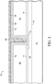
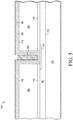
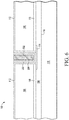
- FIG. 1 through FIG. 6 illustrate, in simplified cross-sectional views, various stages of manufacture of an exemplary through substrate via formed in accordance with an embodiment of the present disclosure.
- a high aspect ratio through substrate via TSV
- metallization steps provide electrical connectivity between a backside surface of the semiconductor device and an interconnect or landing pad embedded in an active portion of the semiconductor device.
- a via plug is then formed with a positive tone photoresist polymer, allowing for a chemical-mechanical planarization (CMP) process to be used to form a planar backside surface of the semiconductor device.
- CMP chemical-mechanical planarization
- the via opening is fabricated by forming an opening through a backside of a semiconductor wafer having a plurality of semiconductor devices (e.g., integrated circuit dies) to expose an underlying metal (e.g., aluminum) layer or structure.
- the via opening is lined with an insulation or dielectric layer, and a metal (e.g., copper) layer by way of an electroplating deposition process.
- the metal layer is subsequently coated with a positive tone photoresist polymer material, the photoresist polymer material fills remaining portion of the via opening.
- the exposed portions of the photoresist are removed in a developer process, leaving the remaining portion of the via opening filled with undeveloped photoresist.
- the Cu liner layer is not oxidized as traditionally experienced with an oxide based plasma etch/strip step.
- the undeveloped photoresist forms a stabilized plug by way of a hard-bake step.
- the backside surface is prepped for subsequent metallization steps using the CMP process.
- the exemplary embodiments can be used to fabricate TSV interconnects in three dimensional (3D) packaging, such as, for example, interposers, wafer level packaging, system in package (SiP) and package on package (PoP) applications, among others.
- 3D three dimensional
- FIGs. 1-6 illustrate, in simplified cross-sectional views, various stages of manufacture of an exemplary through substrate via (TSV) 100 formed in accordance with an embodiment of the present disclosure.
- Topside or active surfaces of semiconductor device 102 and sensor device 104 are affixed to one another at interface 118. Bonding pads, conductive posts and seal ring, and the like to form electrical connectivity and hermetic environment between semiconductor device 102 and sensor device 104 are not shown.
- Semiconductor device 102 may be formed of any suitable semiconductor material or combinations of materials, such as gallium arsenide, silicon germanium, semiconductor-on-insulator (SOI), silicon, monocrystalline silicon, the like, and combinations of the above.
- SOI semiconductor-on-insulator
- Semiconductor device 102 may include analog circuitry, digital circuitry, one or more amplifiers, registers, counters, buffers, interfaces, and the like, or any combination of circuitry and functions, for example.
- Sensor device 104 may be used for detecting and/or measuring motion, pressure, acceleration, and the like.
- Sensor device 104 may include one or more micro-electro-mechanical systems (MEMS) formed in a silicon substrate, for example.
- MEMS micro-electro-mechanical systems
- sensor device 104 may be a second semiconductor device and include circuitry for detecting and/or measuring temperature, for example.
- FIG. 1 illustrates in a simplified cross-sectional view, exemplary TSV 100 at a stage of manufacture in accordance with an embodiment of the present disclosure.
- Exemplary TSV 100 may be characterized as a high aspect ratio TSV having depth-to-diameter ratios of 8:1 and greater, for example.
- TSV 100 may have a depth-to-diameter ratio of 10:1.
- Semiconductor device 102 depicted as one of a plurality of semiconductor devices of a semiconductor wafer, includes a bulk substrate portion 106 and an active portion 108.
- the active portion 108 of semiconductor device 102 may include active components, circuitry, and interconnections between input/output terminals, transistors, resistors, capacitors, and the like.
- a buried dielectric (e.g., oxide) layer 110 is formed between the bulk substrate portion 106 and the active portion 108.
- a vertical via opening 120 is etched into the bulk substrate portion 106 from backside of semiconductor device 102.
- the via etch is initially stopped on the buried dielectric layer 110.
- the via opening 120 in exemplary embodiments may have depths approximately 100 microns and larger and diameters approximately 10 microns and larger.
- PECVD plasma-enhanced chemical vapor deposition
- Metal landing structure 114 may be formed from a variety of electrically conductive materials including, for example, copper, gold, silver, aluminum, nickel, tungsten, and alloys thereof.
- FIG. 2 illustrates in a simplified cross-sectional view, exemplary TSV 100 at a subsequent stage of manufacture in accordance with an embodiment of the present disclosure.
- a barrier layer 202 is deposited by way of an electroless plating process.
- the barrier layer 202 may include titanium (Ti), titanium nitride (TiN), tantalum (Ta), tantalum nitride (TaN), nickel (Ni), cobalt (Co), boron (B), or any suitable combination of these and other materials.
- the barrier layer includes nickel boron (NiB) material and also serves as a seed layer for plating or metallization.
- a conductive liner layer 204 is deposited over barrier layer 202 by way of an electroplating process.
- a copper (Cu) layer is deposited as the liner layer 204 over the barrier layer 202.
- FIG. 3 illustrates in a simplified cross-sectional view, exemplary TSV 100 at a subsequent stage of manufacture in accordance with an embodiment of the present disclosure.
- a polymer layer 302 is applied to the backside surface of semiconductor device 102, filling the reduced via opening (206).
- a positive tone photoresist polymer (e.g., AZ® P4000 or the like) 302 is spin-coated on the backside surface of semiconductor device 102 and vacuum baked to facilitate photoresist polymer 302 flowing into and filling the reduced via opening (206).
- FIG. 4 illustrates in a simplified cross-sectional view, exemplary TSV 100 at a subsequent stage of manufacture in accordance with an embodiment of the present disclosure.
- the photoresist polymer coated backside surface of semiconductor device 102 is irradiated with ultraviolet (UV) light 402.
- UV ultraviolet
- the photoresist polymer coating is characterized as a positive tone photoresist.
- the UV exposed photoresist polymer 404 at the backside surface is removed in a developer step.
- the portion of photoresist polymer 302 which fills the reduced via opening (206) is below developed photoresist 404, and therefore remains undeveloped.
- the Cu liner layer is not oxidized as traditionally experienced with an oxide based plasma etch/strip step.
- the dose and focus of the UV exposure can be adjusted to control the height of photoresist polymer 302 inside the via after develop.
- the final height of photoresist polymer 302 inside the via should be approximately level with an outer surface of the dielectric layer 112 at the backside surface of semiconductor device 102.
- FIG. 5 illustrates in a simplified cross-sectional view, exemplary TSV 100 at a subsequent stage of manufacture in accordance with an embodiment of the present disclosure.
- photoresist polymer develop, only the portion of photoresist polymer 302 inside the via remains.
- the remaining photoresist polymer 302 is hard-baked to cross-link the photoresist polymer forming a permanent via filling material 502.
- shrinkage of the hard-baked polymer 502 may result from being subjected higher temperatures. Such shrinkage may be anticipated and taken into consideration when determining the dose and focus of the UV exposure to set the height of hard-baked polymer 502.
- the final height of the hard-baked polymer 502 inside the via should be substantially level with a top surface of the dielectric layer 112 at the backside surface of semiconductor device 102.
- FIG. 6 illustrates in a simplified cross-sectional view, exemplary TSV 100 at a subsequent stage of manufacture in accordance with an embodiment of the present disclosure.
- a method of forming a through substrate via (TSV) in a semiconductor substrate including etching a vertical via opening into the backside of semiconductor substrate, the via opening exposing a surface of an embedded metal landing structure; depositing a conductive layer over the backside of semiconductor substrate, sidewalls of the via opening, and exposed surface of the metal landing structure; coating the conductive layer with a photoresist polymer material, the photoresist polymer material filling remaining portion of the via opening; developing the photoresist polymer material to remove the photoresist polymer material from the backside of semiconductor substrate and leaving the remaining portion of the via opening substantially filled with undeveloped photoresist polymer material; and forming a planar backside surface of semiconductor substrate by removing the conductive layer deposited over the backside of semiconductor substrate.
- TSV through substrate via
- the method may further include forming a barrier layer between the semiconductor substrate and the conductive layer.
- the barrier layer may include nickel boron (NiB) material and may serve as a seed layer.
- Depositing a conductive layer may include electroplating copper (Cu) on the barrier layer.
- the method may further include irradiating the photoresist polymer material with ultraviolet (UV) light at the backside of semiconductor substrate.
- the photoresist polymer material may be characterized as a positive tone photoresist polymer material.
- the method may further include hard-baking the undeveloped photoresist polymer material to cross-link the photoresist polymer material.
- Forming a planar backside surface of semiconductor substrate may include forming a planar backside surface by removing conductive and barrier layers using a chemical-mechanical planarization (CMP) process.
- the metal landing structure may include a copper (Cu) or aluminum (Al) material.
- a method of forming a through substrate via (TSV) in a semiconductor substrate including etching a vertical via opening into the backside of semiconductor substrate, the via opening exposing a surface of an embedded metal landing structure; depositing a dielectric layer over the backside of semiconductor substrate and sidewalls of the via opening; depositing a conductive layer over the dielectric layer and exposed surface of the metal landing structure; coating the conductive layer with a photoresist polymer material, the photoresist polymer material filling remaining portion of the via opening; developing the photoresist polymer material to remove the photoresist polymer material from the backside of semiconductor substrate and leaving the remaining portion of the via opening substantially filled with undeveloped photoresist polymer; and using a chemical-mechanical planarization (CMP) process to remove conductive layer over the backside of semiconductor substrate, leaving underlying dielectric layer substantially intact.
- CMP chemical-mechanical planarization
- the vertical via opening may be characterized as a high aspect ratio via opening having a depth-to-diameter ratio of substantially 8:1 or greater.
- the method may further include forming a barrier layer between the dielectric layer and the conductive layer.
- the barrier layer may include nickel boron (NiB) material and may serve as a seed layer.
- Depositing a conductive layer may include electroplating copper (Cu) on the barrier layer.
- the photoresist polymer material may be characterized as a positive tone photoresist polymer material.
- the method may further include hard-baking the undeveloped photoresist polymer material to cross-link the photoresist polymer material.
- a semiconductor device including a semiconductor substrate having an active side and a backside; a metal landing structure embedded in the active side; a via opening formed in the backside of the semiconductor substrate, the via opening exposing a surface of the metal landing structure; a conductive layer formed over the sidewalls of the via opening and exposed surface of the metal landing structure; and a photoresist polymer material disposed within the via opening, a surface of the photoresist polymer in the same plane as a surface of the backside of the semiconductor substrate.
- the via opening may be characterized as a high aspect ratio via opening having a depth-to-diameter ratio of substantially 8:1 or greater.
- the conductive layer may include a copper (Cu) material.
- the photoresist polymer material may be characterized as hard-baked positive tone photoresist polymer material.
- a high aspect ratio through substrate via TSV
- metallization steps provide electrical connectivity between a backside surface of the semiconductor device and an interconnect or landing pad embedded in an active portion of the semiconductor device.
- a via plug is then formed with a positive tone photoresist polymer, allowing for a chemical-mechanical planarization (CMP) process to be used to form a planar backside surface of the semiconductor device.
- CMP chemical-mechanical planarization
Landscapes
- Internal Circuitry In Semiconductor Integrated Circuit Devices (AREA)
Abstract
Description
- This disclosure relates generally to semiconductor structures, and more specifically, to through substrate vias (TSV) and methods of forming the same.
- Semiconductor devices are often found in a large spectrum of electronic products - from sewing machines to washing machines, from automobiles to cellular telephones, and so on. These semiconductor devices are typically mounted on a substrate such as a printed circuit board. In order to keep product costs low or to reduce product costs, it is common to minimize the amount of material used within the product, frequently reducing the size of the product itself. As electronic products are reduced in size, printed circuit board real estate becomes more precious putting additional constraints on the size, number, and features of semiconductor devices - pin count, higher integration, package-on-package arrangements, and so on.
- Through substrate vias (TSV) provide an alternative to wire bonds and flip chips, allowing semiconductor devices to be formed by vertically stacking two or more semiconductor chips. A TSV is a vertical electrical interconnect that passes through a device wafer or other semiconductor substrate and facilitates electrical connections between two or more vertically stacked wafers and/or chips. However, TSV fabrication is impacted by associated process constraints, complexity, and resulting yield.
- The present invention is illustrated by way of example and is not limited by the accompanying figures, in which like references indicate similar elements. Elements in the figures are illustrated for simplicity and clarity and have not necessarily been drawn to scale.
-
FIG. 1 through FIG. 6 illustrate, in simplified cross-sectional views, various stages of manufacture of an exemplary through substrate via formed in accordance with an embodiment of the present disclosure. - Generally, there is provided, a high aspect ratio through substrate via (TSV) and method of forming the same. After forming a via opening, metallization steps provide electrical connectivity between a backside surface of the semiconductor device and an interconnect or landing pad embedded in an active portion of the semiconductor device. A via plug is then formed with a positive tone photoresist polymer, allowing for a chemical-mechanical planarization (CMP) process to be used to form a planar backside surface of the semiconductor device.
- In exemplary embodiments, the via opening is fabricated by forming an opening through a backside of a semiconductor wafer having a plurality of semiconductor devices (e.g., integrated circuit dies) to expose an underlying metal (e.g., aluminum) layer or structure. The via opening is lined with an insulation or dielectric layer, and a metal (e.g., copper) layer by way of an electroplating deposition process. The metal layer is subsequently coated with a positive tone photoresist polymer material, the photoresist polymer material fills remaining portion of the via opening. The exposed portions of the photoresist are removed in a developer process, leaving the remaining portion of the via opening filled with undeveloped photoresist. By removing exposed portions in the developer step, the Cu liner layer is not oxidized as traditionally experienced with an oxide based plasma etch/strip step. The undeveloped photoresist forms a stabilized plug by way of a hard-bake step. The backside surface is prepped for subsequent metallization steps using the CMP process.
- The exemplary embodiments can be used to fabricate TSV interconnects in three dimensional (3D) packaging, such as, for example, interposers, wafer level packaging, system in package (SiP) and package on package (PoP) applications, among others.
-
FIGs. 1-6 illustrate, in simplified cross-sectional views, various stages of manufacture of an exemplary through substrate via (TSV) 100 formed in accordance with an embodiment of the present disclosure. Topside or active surfaces ofsemiconductor device 102 andsensor device 104 are affixed to one another atinterface 118. Bonding pads, conductive posts and seal ring, and the like to form electrical connectivity and hermetic environment betweensemiconductor device 102 andsensor device 104 are not shown.Semiconductor device 102 may be formed of any suitable semiconductor material or combinations of materials, such as gallium arsenide, silicon germanium, semiconductor-on-insulator (SOI), silicon, monocrystalline silicon, the like, and combinations of the above.Semiconductor device 102 may include analog circuitry, digital circuitry, one or more amplifiers, registers, counters, buffers, interfaces, and the like, or any combination of circuitry and functions, for example.Sensor device 104 may be used for detecting and/or measuring motion, pressure, acceleration, and the like.Sensor device 104 may include one or more micro-electro-mechanical systems (MEMS) formed in a silicon substrate, for example. In some embodiments,sensor device 104 may be a second semiconductor device and include circuitry for detecting and/or measuring temperature, for example. -
FIG. 1 illustrates in a simplified cross-sectional view,exemplary TSV 100 at a stage of manufacture in accordance with an embodiment of the present disclosure. Exemplary TSV 100 may be characterized as a high aspect ratio TSV having depth-to-diameter ratios of 8:1 and greater, for example. In this embodiment, TSV 100 may have a depth-to-diameter ratio of 10:1.Semiconductor device 102, depicted as one of a plurality of semiconductor devices of a semiconductor wafer, includes abulk substrate portion 106 and anactive portion 108. For example, theactive portion 108 ofsemiconductor device 102 may include active components, circuitry, and interconnections between input/output terminals, transistors, resistors, capacitors, and the like. A buried dielectric (e.g., oxide)layer 110 is formed between thebulk substrate portion 106 and theactive portion 108. As illustrated inFIG. 1 , a vertical viaopening 120 is etched into thebulk substrate portion 106 from backside ofsemiconductor device 102. The via etch is initially stopped on the burieddielectric layer 110. The via opening 120 in exemplary embodiments may have depths approximately 100 microns and larger and diameters approximately 10 microns and larger. Subsequently, plasma-enhanced chemical vapor deposition (PECVD) oxide is deposited and etched in repeated cycles to expose a surface ofmetal landing structure 114 and to formdielectric layer 112 on the via opening sidewalls and backside surface ofsemiconductor device 102.Metal landing structure 114 may be formed from a variety of electrically conductive materials including, for example, copper, gold, silver, aluminum, nickel, tungsten, and alloys thereof. -
FIG. 2 illustrates in a simplified cross-sectional view,exemplary TSV 100 at a subsequent stage of manufacture in accordance with an embodiment of the present disclosure. After formation of thedielectric layer 112, abarrier layer 202 is deposited by way of an electroless plating process. Thebarrier layer 202 may include titanium (Ti), titanium nitride (TiN), tantalum (Ta), tantalum nitride (TaN), nickel (Ni), cobalt (Co), boron (B), or any suitable combination of these and other materials. In this embodiment, the barrier layer includes nickel boron (NiB) material and also serves as a seed layer for plating or metallization. Aconductive liner layer 204 is deposited overbarrier layer 202 by way of an electroplating process. In this embodiment, a copper (Cu) layer is deposited as theliner layer 204 over thebarrier layer 202. After deposition of thebarrier layer 202 andliner layer 204, a slightly reduced via opening 206 remains. -
FIG. 3 illustrates in a simplified cross-sectional view,exemplary TSV 100 at a subsequent stage of manufacture in accordance with an embodiment of the present disclosure. AfterCu liner layer 204 is deposited over thebarrier layer 202, apolymer layer 302 is applied to the backside surface ofsemiconductor device 102, filling the reduced via opening (206). In this embodiment, a positive tone photoresist polymer (e.g., AZ® P4000 or the like) 302 is spin-coated on the backside surface ofsemiconductor device 102 and vacuum baked to facilitatephotoresist polymer 302 flowing into and filling the reduced via opening (206). -
FIG. 4 illustrates in a simplified cross-sectional view,exemplary TSV 100 at a subsequent stage of manufacture in accordance with an embodiment of the present disclosure. As illustrated, the photoresist polymer coated backside surface ofsemiconductor device 102 is irradiated with ultraviolet (UV)light 402. In this embodiment, the photoresist polymer coating is characterized as a positive tone photoresist. After the photoresist polymer is exposed toUV light 402, the UV exposedphotoresist polymer 404 at the backside surface is removed in a developer step. The portion ofphotoresist polymer 302 which fills the reduced via opening (206) is below developedphotoresist 404, and therefore remains undeveloped. In this embodiment, because the positive tone photoresist allowed for removal of UV exposed portions in the developer step, the Cu liner layer is not oxidized as traditionally experienced with an oxide based plasma etch/strip step. The dose and focus of the UV exposure can be adjusted to control the height ofphotoresist polymer 302 inside the via after develop. The final height ofphotoresist polymer 302 inside the via should be approximately level with an outer surface of thedielectric layer 112 at the backside surface ofsemiconductor device 102. -
FIG. 5 illustrates in a simplified cross-sectional view,exemplary TSV 100 at a subsequent stage of manufacture in accordance with an embodiment of the present disclosure. After photoresist polymer develop, only the portion ofphotoresist polymer 302 inside the via remains. The remainingphotoresist polymer 302 is hard-baked to cross-link the photoresist polymer forming a permanent viafilling material 502. During the hard-bake ofphotoresist polymer 302, shrinkage of the hard-baked polymer 502 may result from being subjected higher temperatures. Such shrinkage may be anticipated and taken into consideration when determining the dose and focus of the UV exposure to set the height of hard-baked polymer 502. The final height of the hard-baked polymer 502 inside the via should be substantially level with a top surface of thedielectric layer 112 at the backside surface ofsemiconductor device 102. -
FIG. 6 illustrates in a simplified cross-sectional view,exemplary TSV 100 at a subsequent stage of manufacture in accordance with an embodiment of the present disclosure. After hard-baking the remainingphotoresist polymer 302 to form a permanent viafilling material 502, the Cu and NiB layers at the backside surface ofsemiconductor device 102 are removed. A chemical-mechanical planarization (CMP) process is used to remove the Cu and NiB layers, keeping thedielectric layer 112 intact. After the CMP step, a planar surface results across the backside surface ofsemiconductor device 102 allowing for subsequent metallization steps interconnecting theexemplary TSV 100. - Generally, there is provided, a method of forming a through substrate via (TSV) in a semiconductor substrate, including etching a vertical via opening into the backside of semiconductor substrate, the via opening exposing a surface of an embedded metal landing structure; depositing a conductive layer over the backside of semiconductor substrate, sidewalls of the via opening, and exposed surface of the metal landing structure; coating the conductive layer with a photoresist polymer material, the photoresist polymer material filling remaining portion of the via opening; developing the photoresist polymer material to remove the photoresist polymer material from the backside of semiconductor substrate and leaving the remaining portion of the via opening substantially filled with undeveloped photoresist polymer material; and forming a planar backside surface of semiconductor substrate by removing the conductive layer deposited over the backside of semiconductor substrate. The method may further include forming a barrier layer between the semiconductor substrate and the conductive layer. The barrier layer may include nickel boron (NiB) material and may serve as a seed layer. Depositing a conductive layer may include electroplating copper (Cu) on the barrier layer. The method may further include irradiating the photoresist polymer material with ultraviolet (UV) light at the backside of semiconductor substrate. The photoresist polymer material may be characterized as a positive tone photoresist polymer material. The method may further include hard-baking the undeveloped photoresist polymer material to cross-link the photoresist polymer material. Forming a planar backside surface of semiconductor substrate may include forming a planar backside surface by removing conductive and barrier layers using a chemical-mechanical planarization (CMP) process. The metal landing structure may include a copper (Cu) or aluminum (Al) material.
- In another embodiment, there is provided, a method of forming a through substrate via (TSV) in a semiconductor substrate, including etching a vertical via opening into the backside of semiconductor substrate, the via opening exposing a surface of an embedded metal landing structure; depositing a dielectric layer over the backside of semiconductor substrate and sidewalls of the via opening; depositing a conductive layer over the dielectric layer and exposed surface of the metal landing structure; coating the conductive layer with a photoresist polymer material, the photoresist polymer material filling remaining portion of the via opening; developing the photoresist polymer material to remove the photoresist polymer material from the backside of semiconductor substrate and leaving the remaining portion of the via opening substantially filled with undeveloped photoresist polymer; and using a chemical-mechanical planarization (CMP) process to remove conductive layer over the backside of semiconductor substrate, leaving underlying dielectric layer substantially intact. The vertical via opening may be characterized as a high aspect ratio via opening having a depth-to-diameter ratio of substantially 8:1 or greater. The method may further include forming a barrier layer between the dielectric layer and the conductive layer. The barrier layer may include nickel boron (NiB) material and may serve as a seed layer. Depositing a conductive layer may include electroplating copper (Cu) on the barrier layer. The photoresist polymer material may be characterized as a positive tone photoresist polymer material. The method may further include hard-baking the undeveloped photoresist polymer material to cross-link the photoresist polymer material.
- In yet another embodiment, there is provided, a semiconductor device including a semiconductor substrate having an active side and a backside; a metal landing structure embedded in the active side; a via opening formed in the backside of the semiconductor substrate, the via opening exposing a surface of the metal landing structure; a conductive layer formed over the sidewalls of the via opening and exposed surface of the metal landing structure; and a photoresist polymer material disposed within the via opening, a surface of the photoresist polymer in the same plane as a surface of the backside of the semiconductor substrate. The via opening may be characterized as a high aspect ratio via opening having a depth-to-diameter ratio of substantially 8:1 or greater. The conductive layer may include a copper (Cu) material. The photoresist polymer material may be characterized as hard-baked positive tone photoresist polymer material.
- By now it should be appreciated that there has been provided, a high aspect ratio through substrate via (TSV) and method of forming the same. After forming a via opening, metallization steps provide electrical connectivity between a backside surface of the semiconductor device and an interconnect or landing pad embedded in an active portion of the semiconductor device. A via plug is then formed with a positive tone photoresist polymer, allowing for a chemical-mechanical planarization (CMP) process to be used to form a planar backside surface of the semiconductor device.
- Although the invention is described herein with reference to specific embodiments, various modifications and changes can be made without departing from the scope of the present invention as set forth in the claims below. Accordingly, the specification and figures are to be regarded in an illustrative rather than a restrictive sense, and all such modifications are intended to be included within the scope of the present invention. Any benefits, advantages, or solutions to problems that are described herein with regard to specific embodiments are not intended to be construed as a critical, required, or essential feature or element of any or all the claims.
- The terms "front," "back," "top," "bottom," "over," "under" and the like in the description and in the claims, if any, are used for descriptive purposes and not necessarily for describing permanent relative positions. It is understood that the terms so used are interchangeable under appropriate circumstances such that the embodiments of the invention described herein are, for example, capable of operation in other orientations than those illustrated or otherwise described herein.
- Furthermore, the terms "a" or "an," as used herein, are defined as one or more than one. Also, the use of introductory phrases such as "at least one" and "one or more" in the claims should not be construed to imply that the introduction of another claim element by the indefinite articles "a" or "an" limits any particular claim containing such introduced claim element to inventions containing only one such element, even when the same claim includes the introductory phrases "one or more" or "at least one" and indefinite articles such as "a" or "an." The same holds true for the use of definite articles.
- Unless stated otherwise, terms such as "first" and "second" are used to arbitrarily distinguish between the elements such terms describe. Thus, these terms are not necessarily intended to indicate temporal or other prioritization of such elements.
Claims (15)
- A method of forming a through substrate via, TSV, in a semiconductor substrate, comprising:etching a vertical via opening (120) into the backside of semiconductor substrate, the via opening (120) exposing a surface of an embedded metal landing structure (114);depositing a conductive layer (204) over the backside of semiconductor substrate, sidewalls of the via opening (120), and exposed surface of the metal landing structure (114);coating the conductive layer (204) with a photoresist polymer material (302), the photoresist polymer material (302) filling remaining portion of the via opening (120);developing the photoresist polymer material (302) to remove the photoresist polymer material (302) from the backside of semiconductor substrate and leaving the remaining portion of the via opening (120) substantially filled with undeveloped photoresist polymer material (302); andforming a planar backside surface of semiconductor substrate by removing the conductive layer (204) deposited over the backside of semiconductor substrate.
- The method of claim 1, further comprising forming a barrier layer (202) between the semiconductor substrate and the conductive layer (204).
- The method of claim 2, wherein the barrier layer (202) includes nickel boron, NiB, material and serves as a seed layer.
- The method of claim 2 or claim 3, wherein depositing the conductive layer (204) includes electroplating copper, Cu, on the barrier layer (202).
- The method of any one of the claims 1 to 4, further comprising irradiating the photoresist polymer material (302) with ultraviolet, UV, light (402) at the backside of semiconductor substrate.
- The method of any one of the claims 1 to 5, wherein the photoresist polymer material (302) is characterized as a positive tone photoresist polymer material.
- The method of any one of the claims 1 to 6, further comprising hard-baking the undeveloped photoresist polymer material (302) to cross-link the photoresist polymer material.
- The method of any one of the claims 1 to 7, wherein forming a planar backside surface of semiconductor substrate includes forming a planar backside surface by removing conductive and barrier layers (204, 202) using a chemical-mechanical planarization, CMP, process.
- A method of forming a through substrate via, TSV, in a semiconductor substrate, comprising:etching a vertical via opening (120) into the backside of semiconductor substrate, the via opening (120) exposing a surface of an embedded metal landing structure (114);depositing a dielectric layer (112) over the backside of semiconductor substrate and sidewalls of the via opening (120);depositing a conductive layer (204) over the dielectric layer (112) and exposed surface of the metal landing structure (114);coating the conductive layer (204) with a photoresist polymer material (302), the photoresist polymer material (302) filling remaining portion of the via opening (120);developing the photoresist polymer material (302) to remove the photoresist polymer material (302) from the backside of semiconductor substrate and leaving the remaining portion of the via opening (120) substantially filled with undeveloped photoresist polymer (302); andusing a chemical-mechanical planarization (CMP) process to remove conductive layer (204) over the backside of semiconductor substrate, leaving underlying dielectric layer (112) substantially intact.
- The method of claim 9, further comprising forming a barrier layer (202) between the dielectric layer (112) and the conductive layer (204).
- The method of claim 9 or claim 10, further comprising hard-baking the undeveloped photoresist polymer material (302) to cross-link the photoresist polymer material.
- A semiconductor device, comprising:a semiconductor substrate having an active side and a backside;a metal landing structure (114) embedded in the active side;a via opening (120) formed in the backside of the semiconductor substrate, the via opening (120) exposing a surface of the metal landing structure (114);a conductive layer (204) formed over the sidewalls of the via opening (120) and exposed surface of the metal landing structure (114); anda photoresist polymer material (302) disposed within the via opening (120), a surface of the photoresist polymer in the same plane as a surface of the backside of the semiconductor substrate.
- The semiconductor device of claim 12, wherein the via opening (120) is characterized as a high aspect ratio via opening (120) having a depth-to-diameter ratio of substantially 8:1 or greater.
- The semiconductor device of claim 12 or claim 13, wherein the conductive layer (204) comprises a copper, Cu, material.
- The semiconductor device of any one of the claims 12 to 14, wherein the photoresist polymer material (302) is characterized as hard-baked positive tone photoresist polymer material.
Applications Claiming Priority (1)
| Application Number | Priority Date | Filing Date | Title |
|---|---|---|---|
| US15/335,875 US10157792B2 (en) | 2016-10-27 | 2016-10-27 | Through substrate via (TSV) and method therefor |
Publications (2)
| Publication Number | Publication Date |
|---|---|
| EP3316283A1 true EP3316283A1 (en) | 2018-05-02 |
| EP3316283B1 EP3316283B1 (en) | 2021-03-03 |
Family
ID=58765745
Family Applications (1)
| Application Number | Title | Priority Date | Filing Date |
|---|---|---|---|
| EP17172306.7A Active EP3316283B1 (en) | 2016-10-27 | 2017-05-22 | Method of fabricating a through substrate via |
Country Status (2)
| Country | Link |
|---|---|
| US (2) | US10157792B2 (en) |
| EP (1) | EP3316283B1 (en) |
Families Citing this family (9)
| Publication number | Priority date | Publication date | Assignee | Title |
|---|---|---|---|---|
| US9658281B2 (en) * | 2013-10-25 | 2017-05-23 | Taiwan Semiconductor Manufacturing Company Limited | Alignment testing for tiered semiconductor structure |
| US10796995B2 (en) * | 2017-11-29 | 2020-10-06 | Tohoku University | Semiconductor devices including a first cobalt alloy in a first barrier layer and a second cobalt alloy in a second barrier layer |
| KR102576062B1 (en) | 2018-11-07 | 2023-09-07 | 삼성전자주식회사 | A semiconductor device having a through silicon via and method of manufacturing the same |
| US11605576B2 (en) * | 2019-06-25 | 2023-03-14 | Semiconductor Components Industries, Llc | Via for semiconductor devices and related methods |
| US11322458B2 (en) * | 2020-04-27 | 2022-05-03 | Nanya Technology Corporation | Semiconductor structure including a first substrate and a second substrate and a buffer structure in the second substrate |
| US11450616B2 (en) | 2020-07-29 | 2022-09-20 | Nxp Usa, Inc. | Using a backside mask layer for forming a unique die mark identifier pattern |
| US12112792B2 (en) * | 2021-08-10 | 2024-10-08 | Micron Technology, Inc. | Memory device for wafer-on-wafer formed memory and logic |
| KR20240009073A (en) * | 2022-07-13 | 2024-01-22 | 에스케이하이닉스 주식회사 | Image sensing device including through electrode structure |
| CN119812111A (en) * | 2024-12-27 | 2025-04-11 | 赛莱克斯微系统科技(北京)有限公司 | Method for manufacturing through silicon via wafer and semiconductor manufacturing method |
Citations (4)
| Publication number | Priority date | Publication date | Assignee | Title |
|---|---|---|---|---|
| US5350662A (en) * | 1992-03-26 | 1994-09-27 | Hughes Aircraft Company | Maskless process for forming refractory metal layer in via holes of GaAs chips |
| US20070045780A1 (en) * | 2005-09-01 | 2007-03-01 | Salman Akram | Methods of forming blind wafer interconnects, and related structures and assemblies |
| US20090134498A1 (en) * | 2007-11-20 | 2009-05-28 | Elpida Memory, Inc. | Semiconductor apparatus |
| WO2011125935A1 (en) * | 2010-04-05 | 2011-10-13 | 株式会社フジクラ | Semiconductor device and manufacturing method thereof |
Family Cites Families (6)
| Publication number | Priority date | Publication date | Assignee | Title |
|---|---|---|---|---|
| KR101424824B1 (en) * | 2005-11-18 | 2014-08-01 | 레플리서러스 그룹 에스에이에스 | Method of forming a multilayer structure |
| US7917132B2 (en) * | 2006-12-18 | 2011-03-29 | Broadcom Corporation | Direct memory download in a voice data and RF integrated circuit and method for use therewith |
| US7964502B2 (en) * | 2008-11-25 | 2011-06-21 | Freescale Semiconductor, Inc. | Multilayered through via |
| US9714474B2 (en) * | 2010-04-06 | 2017-07-25 | Tel Nexx, Inc. | Seed layer deposition in microscale features |
| US8836116B2 (en) * | 2010-10-21 | 2014-09-16 | Taiwan Semiconductor Manufacturing Company, Ltd. | Wafer level packaging of micro-electro-mechanical systems (MEMS) and complementary metal-oxide-semiconductor (CMOS) substrates |
| US20130249047A1 (en) * | 2012-03-26 | 2013-09-26 | Nanya Technology Corporation | Through silicon via structure and method for fabricating the same |
-
2016
- 2016-10-27 US US15/335,875 patent/US10157792B2/en active Active
-
2017
- 2017-05-22 EP EP17172306.7A patent/EP3316283B1/en active Active
-
2018
- 2018-11-01 US US16/177,673 patent/US10546779B2/en active Active
Patent Citations (4)
| Publication number | Priority date | Publication date | Assignee | Title |
|---|---|---|---|---|
| US5350662A (en) * | 1992-03-26 | 1994-09-27 | Hughes Aircraft Company | Maskless process for forming refractory metal layer in via holes of GaAs chips |
| US20070045780A1 (en) * | 2005-09-01 | 2007-03-01 | Salman Akram | Methods of forming blind wafer interconnects, and related structures and assemblies |
| US20090134498A1 (en) * | 2007-11-20 | 2009-05-28 | Elpida Memory, Inc. | Semiconductor apparatus |
| WO2011125935A1 (en) * | 2010-04-05 | 2011-10-13 | 株式会社フジクラ | Semiconductor device and manufacturing method thereof |
Also Published As
| Publication number | Publication date |
|---|---|
| EP3316283B1 (en) | 2021-03-03 |
| US20190074220A1 (en) | 2019-03-07 |
| US10546779B2 (en) | 2020-01-28 |
| US10157792B2 (en) | 2018-12-18 |
| US20180122698A1 (en) | 2018-05-03 |
Similar Documents
| Publication | Publication Date | Title |
|---|---|---|
| US10546779B2 (en) | Through substrate via (TSV) and method therefor | |
| US7453150B1 (en) | Three-dimensional face-to-face integration assembly | |
| Tezcan et al. | Sloped through wafer vias for 3D wafer level packaging | |
| US11830841B2 (en) | Semiconductor package and method for manufacturing the same | |
| US8841755B2 (en) | Through silicon via and method of forming the same | |
| US11715681B2 (en) | Fan-out package structure and method | |
| US20120098122A1 (en) | Wafer level packaging of micro-electro-mechanical systems (mems) and complementary metal-oxide-semiconductor (cmos) substrates | |
| US10886244B2 (en) | Collars for under-bump metal structures and associated systems and methods | |
| US10910345B2 (en) | Semiconductor device with stacked die device | |
| US20140264921A1 (en) | Through-silicon via with sidewall air gap | |
| US20150145144A1 (en) | Use of a conformal coating elastic cushion to reduce through silicon vias (tsv) stress in 3-dimensional integration | |
| US10797005B2 (en) | Semiconductor package and method for manufacturing the same | |
| CN108122858A (en) | Packaging structure | |
| WO2012096909A2 (en) | Alignment marks to enable 3d integration | |
| CN113451236B (en) | Method for constructing sensing chip packaging structure | |
| TWI749920B (en) | Semicondutor package and method of forming same | |
| CN114551338A (en) | Semiconductor device having buried metal pad and method of manufacturing the same | |
| US9257335B2 (en) | Electronic devices utilizing contact pads with protrusions and methods for fabrication | |
| CN108807197A (en) | Chip package with sidewall metallization portion | |
| Lai et al. | A ‘mesh’seed layer for improved through-silicon-via fabrication | |
| TWI855966B (en) | Semiconductor device and method of manufacturing the same | |
| CN118610097A (en) | Packaging device and method of forming the same | |
| Zoschke et al. | Wafer level 3D system integration based on silicon interposers with through silicon vias | |
| US20240312857A1 (en) | Semiconductor structure and method of fabricating same |
Legal Events
| Date | Code | Title | Description |
|---|---|---|---|
| PUAI | Public reference made under article 153(3) epc to a published international application that has entered the european phase |
Free format text: ORIGINAL CODE: 0009012 |
|
| STAA | Information on the status of an ep patent application or granted ep patent |
Free format text: STATUS: THE APPLICATION HAS BEEN PUBLISHED |
|
| AK | Designated contracting states |
Kind code of ref document: A1 Designated state(s): AL AT BE BG CH CY CZ DE DK EE ES FI FR GB GR HR HU IE IS IT LI LT LU LV MC MK MT NL NO PL PT RO RS SE SI SK SM TR |
|
| AX | Request for extension of the european patent |
Extension state: BA ME |
|
| STAA | Information on the status of an ep patent application or granted ep patent |
Free format text: STATUS: REQUEST FOR EXAMINATION WAS MADE |
|
| 17P | Request for examination filed |
Effective date: 20181102 |
|
| RBV | Designated contracting states (corrected) |
Designated state(s): AL AT BE BG CH CY CZ DE DK EE ES FI FR GB GR HR HU IE IS IT LI LT LU LV MC MK MT NL NO PL PT RO RS SE SI SK SM TR |
|
| STAA | Information on the status of an ep patent application or granted ep patent |
Free format text: STATUS: EXAMINATION IS IN PROGRESS |
|
| 17Q | First examination report despatched |
Effective date: 20200625 |
|
| GRAP | Despatch of communication of intention to grant a patent |
Free format text: ORIGINAL CODE: EPIDOSNIGR1 |
|
| STAA | Information on the status of an ep patent application or granted ep patent |
Free format text: STATUS: GRANT OF PATENT IS INTENDED |
|
| INTG | Intention to grant announced |
Effective date: 20200928 |
|
| GRAS | Grant fee paid |
Free format text: ORIGINAL CODE: EPIDOSNIGR3 |
|
| GRAA | (expected) grant |
Free format text: ORIGINAL CODE: 0009210 |
|
| STAA | Information on the status of an ep patent application or granted ep patent |
Free format text: STATUS: THE PATENT HAS BEEN GRANTED |
|
| AK | Designated contracting states |
Kind code of ref document: B1 Designated state(s): AL AT BE BG CH CY CZ DE DK EE ES FI FR GB GR HR HU IE IS IT LI LT LU LV MC MK MT NL NO PL PT RO RS SE SI SK SM TR |
|
| REG | Reference to a national code |
Ref country code: GB Ref legal event code: FG4D |
|
| REG | Reference to a national code |
Ref country code: AT Ref legal event code: REF Ref document number: 1368137 Country of ref document: AT Kind code of ref document: T Effective date: 20210315 Ref country code: CH Ref legal event code: EP |
|
| REG | Reference to a national code |
Ref country code: DE Ref legal event code: R096 Ref document number: 602017033649 Country of ref document: DE |
|
| REG | Reference to a national code |
Ref country code: IE Ref legal event code: FG4D |
|
| REG | Reference to a national code |
Ref country code: LT Ref legal event code: MG9D |
|
| PG25 | Lapsed in a contracting state [announced via postgrant information from national office to epo] |
Ref country code: LT Free format text: LAPSE BECAUSE OF FAILURE TO SUBMIT A TRANSLATION OF THE DESCRIPTION OR TO PAY THE FEE WITHIN THE PRESCRIBED TIME-LIMIT Effective date: 20210303 Ref country code: BG Free format text: LAPSE BECAUSE OF FAILURE TO SUBMIT A TRANSLATION OF THE DESCRIPTION OR TO PAY THE FEE WITHIN THE PRESCRIBED TIME-LIMIT Effective date: 20210603 Ref country code: NO Free format text: LAPSE BECAUSE OF FAILURE TO SUBMIT A TRANSLATION OF THE DESCRIPTION OR TO PAY THE FEE WITHIN THE PRESCRIBED TIME-LIMIT Effective date: 20210603 Ref country code: GR Free format text: LAPSE BECAUSE OF FAILURE TO SUBMIT A TRANSLATION OF THE DESCRIPTION OR TO PAY THE FEE WITHIN THE PRESCRIBED TIME-LIMIT Effective date: 20210604 Ref country code: FI Free format text: LAPSE BECAUSE OF FAILURE TO SUBMIT A TRANSLATION OF THE DESCRIPTION OR TO PAY THE FEE WITHIN THE PRESCRIBED TIME-LIMIT Effective date: 20210303 Ref country code: HR Free format text: LAPSE BECAUSE OF FAILURE TO SUBMIT A TRANSLATION OF THE DESCRIPTION OR TO PAY THE FEE WITHIN THE PRESCRIBED TIME-LIMIT Effective date: 20210303 |
|
| REG | Reference to a national code |
Ref country code: NL Ref legal event code: MP Effective date: 20210303 |
|
| REG | Reference to a national code |
Ref country code: AT Ref legal event code: MK05 Ref document number: 1368137 Country of ref document: AT Kind code of ref document: T Effective date: 20210303 |
|
| PG25 | Lapsed in a contracting state [announced via postgrant information from national office to epo] |
Ref country code: SE Free format text: LAPSE BECAUSE OF FAILURE TO SUBMIT A TRANSLATION OF THE DESCRIPTION OR TO PAY THE FEE WITHIN THE PRESCRIBED TIME-LIMIT Effective date: 20210303 Ref country code: LV Free format text: LAPSE BECAUSE OF FAILURE TO SUBMIT A TRANSLATION OF THE DESCRIPTION OR TO PAY THE FEE WITHIN THE PRESCRIBED TIME-LIMIT Effective date: 20210303 Ref country code: PL Free format text: LAPSE BECAUSE OF FAILURE TO SUBMIT A TRANSLATION OF THE DESCRIPTION OR TO PAY THE FEE WITHIN THE PRESCRIBED TIME-LIMIT Effective date: 20210303 Ref country code: RS Free format text: LAPSE BECAUSE OF FAILURE TO SUBMIT A TRANSLATION OF THE DESCRIPTION OR TO PAY THE FEE WITHIN THE PRESCRIBED TIME-LIMIT Effective date: 20210303 |
|
| PG25 | Lapsed in a contracting state [announced via postgrant information from national office to epo] |
Ref country code: NL Free format text: LAPSE BECAUSE OF FAILURE TO SUBMIT A TRANSLATION OF THE DESCRIPTION OR TO PAY THE FEE WITHIN THE PRESCRIBED TIME-LIMIT Effective date: 20210303 |
|
| PG25 | Lapsed in a contracting state [announced via postgrant information from national office to epo] |
Ref country code: SM Free format text: LAPSE BECAUSE OF FAILURE TO SUBMIT A TRANSLATION OF THE DESCRIPTION OR TO PAY THE FEE WITHIN THE PRESCRIBED TIME-LIMIT Effective date: 20210303 Ref country code: AT Free format text: LAPSE BECAUSE OF FAILURE TO SUBMIT A TRANSLATION OF THE DESCRIPTION OR TO PAY THE FEE WITHIN THE PRESCRIBED TIME-LIMIT Effective date: 20210303 Ref country code: EE Free format text: LAPSE BECAUSE OF FAILURE TO SUBMIT A TRANSLATION OF THE DESCRIPTION OR TO PAY THE FEE WITHIN THE PRESCRIBED TIME-LIMIT Effective date: 20210303 Ref country code: CZ Free format text: LAPSE BECAUSE OF FAILURE TO SUBMIT A TRANSLATION OF THE DESCRIPTION OR TO PAY THE FEE WITHIN THE PRESCRIBED TIME-LIMIT Effective date: 20210303 |
|
| PG25 | Lapsed in a contracting state [announced via postgrant information from national office to epo] |
Ref country code: SK Free format text: LAPSE BECAUSE OF FAILURE TO SUBMIT A TRANSLATION OF THE DESCRIPTION OR TO PAY THE FEE WITHIN THE PRESCRIBED TIME-LIMIT Effective date: 20210303 Ref country code: RO Free format text: LAPSE BECAUSE OF FAILURE TO SUBMIT A TRANSLATION OF THE DESCRIPTION OR TO PAY THE FEE WITHIN THE PRESCRIBED TIME-LIMIT Effective date: 20210303 Ref country code: PT Free format text: LAPSE BECAUSE OF FAILURE TO SUBMIT A TRANSLATION OF THE DESCRIPTION OR TO PAY THE FEE WITHIN THE PRESCRIBED TIME-LIMIT Effective date: 20210705 Ref country code: IS Free format text: LAPSE BECAUSE OF FAILURE TO SUBMIT A TRANSLATION OF THE DESCRIPTION OR TO PAY THE FEE WITHIN THE PRESCRIBED TIME-LIMIT Effective date: 20210703 |
|
| REG | Reference to a national code |
Ref country code: DE Ref legal event code: R097 Ref document number: 602017033649 Country of ref document: DE |
|
| REG | Reference to a national code |
Ref country code: CH Ref legal event code: PL |
|
| PLBE | No opposition filed within time limit |
Free format text: ORIGINAL CODE: 0009261 |
|
| STAA | Information on the status of an ep patent application or granted ep patent |
Free format text: STATUS: NO OPPOSITION FILED WITHIN TIME LIMIT |
|
| PG25 | Lapsed in a contracting state [announced via postgrant information from national office to epo] |
Ref country code: MC Free format text: LAPSE BECAUSE OF FAILURE TO SUBMIT A TRANSLATION OF THE DESCRIPTION OR TO PAY THE FEE WITHIN THE PRESCRIBED TIME-LIMIT Effective date: 20210303 Ref country code: LI Free format text: LAPSE BECAUSE OF NON-PAYMENT OF DUE FEES Effective date: 20210531 Ref country code: LU Free format text: LAPSE BECAUSE OF NON-PAYMENT OF DUE FEES Effective date: 20210522 Ref country code: DK Free format text: LAPSE BECAUSE OF FAILURE TO SUBMIT A TRANSLATION OF THE DESCRIPTION OR TO PAY THE FEE WITHIN THE PRESCRIBED TIME-LIMIT Effective date: 20210303 Ref country code: CH Free format text: LAPSE BECAUSE OF NON-PAYMENT OF DUE FEES Effective date: 20210531 Ref country code: AL Free format text: LAPSE BECAUSE OF FAILURE TO SUBMIT A TRANSLATION OF THE DESCRIPTION OR TO PAY THE FEE WITHIN THE PRESCRIBED TIME-LIMIT Effective date: 20210303 Ref country code: ES Free format text: LAPSE BECAUSE OF FAILURE TO SUBMIT A TRANSLATION OF THE DESCRIPTION OR TO PAY THE FEE WITHIN THE PRESCRIBED TIME-LIMIT Effective date: 20210303 |
|
| 26N | No opposition filed |
Effective date: 20211206 |
|
| REG | Reference to a national code |
Ref country code: BE Ref legal event code: MM Effective date: 20210531 |
|
| GBPC | Gb: european patent ceased through non-payment of renewal fee |
Effective date: 20210603 |
|
| PG25 | Lapsed in a contracting state [announced via postgrant information from national office to epo] |
Ref country code: SI Free format text: LAPSE BECAUSE OF FAILURE TO SUBMIT A TRANSLATION OF THE DESCRIPTION OR TO PAY THE FEE WITHIN THE PRESCRIBED TIME-LIMIT Effective date: 20210303 |
|
| PG25 | Lapsed in a contracting state [announced via postgrant information from national office to epo] |
Ref country code: IT Free format text: LAPSE BECAUSE OF FAILURE TO SUBMIT A TRANSLATION OF THE DESCRIPTION OR TO PAY THE FEE WITHIN THE PRESCRIBED TIME-LIMIT Effective date: 20210303 Ref country code: IE Free format text: LAPSE BECAUSE OF NON-PAYMENT OF DUE FEES Effective date: 20210522 Ref country code: GB Free format text: LAPSE BECAUSE OF NON-PAYMENT OF DUE FEES Effective date: 20210603 |
|
| PG25 | Lapsed in a contracting state [announced via postgrant information from national office to epo] |
Ref country code: IS Free format text: LAPSE BECAUSE OF FAILURE TO SUBMIT A TRANSLATION OF THE DESCRIPTION OR TO PAY THE FEE WITHIN THE PRESCRIBED TIME-LIMIT Effective date: 20210703 Ref country code: FR Free format text: LAPSE BECAUSE OF NON-PAYMENT OF DUE FEES Effective date: 20210531 |
|
| PG25 | Lapsed in a contracting state [announced via postgrant information from national office to epo] |
Ref country code: BE Free format text: LAPSE BECAUSE OF NON-PAYMENT OF DUE FEES Effective date: 20210531 |
|
| PG25 | Lapsed in a contracting state [announced via postgrant information from national office to epo] |
Ref country code: CY Free format text: LAPSE BECAUSE OF FAILURE TO SUBMIT A TRANSLATION OF THE DESCRIPTION OR TO PAY THE FEE WITHIN THE PRESCRIBED TIME-LIMIT Effective date: 20210303 |
|
| PG25 | Lapsed in a contracting state [announced via postgrant information from national office to epo] |
Ref country code: HU Free format text: LAPSE BECAUSE OF FAILURE TO SUBMIT A TRANSLATION OF THE DESCRIPTION OR TO PAY THE FEE WITHIN THE PRESCRIBED TIME-LIMIT; INVALID AB INITIO Effective date: 20170522 |
|
| P01 | Opt-out of the competence of the unified patent court (upc) registered |
Effective date: 20230725 |
|
| PG25 | Lapsed in a contracting state [announced via postgrant information from national office to epo] |
Ref country code: MK Free format text: LAPSE BECAUSE OF FAILURE TO SUBMIT A TRANSLATION OF THE DESCRIPTION OR TO PAY THE FEE WITHIN THE PRESCRIBED TIME-LIMIT Effective date: 20210303 |
|
| PG25 | Lapsed in a contracting state [announced via postgrant information from national office to epo] |
Ref country code: TR Free format text: LAPSE BECAUSE OF FAILURE TO SUBMIT A TRANSLATION OF THE DESCRIPTION OR TO PAY THE FEE WITHIN THE PRESCRIBED TIME-LIMIT Effective date: 20210303 |
|
| PG25 | Lapsed in a contracting state [announced via postgrant information from national office to epo] |
Ref country code: MT Free format text: LAPSE BECAUSE OF FAILURE TO SUBMIT A TRANSLATION OF THE DESCRIPTION OR TO PAY THE FEE WITHIN THE PRESCRIBED TIME-LIMIT Effective date: 20210303 |
|
| PGFP | Annual fee paid to national office [announced via postgrant information from national office to epo] |
Ref country code: DE Payment date: 20250423 Year of fee payment: 9 |
|
| REG | Reference to a national code |
Ref country code: DE Ref legal event code: R079 Ref document number: 602017033649 Country of ref document: DE Free format text: PREVIOUS MAIN CLASS: H01L0021768000 Ipc: H10W0020000000 |