EP3316104A1 - Magnetic core coil and electronic pen - Google Patents
Magnetic core coil and electronic pen Download PDFInfo
- Publication number
- EP3316104A1 EP3316104A1 EP16814247.9A EP16814247A EP3316104A1 EP 3316104 A1 EP3316104 A1 EP 3316104A1 EP 16814247 A EP16814247 A EP 16814247A EP 3316104 A1 EP3316104 A1 EP 3316104A1
- Authority
- EP
- European Patent Office
- Prior art keywords
- core
- coil
- axial direction
- terminal members
- magnetic core
- Prior art date
- Legal status (The legal status is an assumption and is not a legal conclusion. Google has not performed a legal analysis and makes no representation as to the accuracy of the status listed.)
- Granted
Links
Images






Classifications
-
- H—ELECTRICITY
- H01—ELECTRIC ELEMENTS
- H01F—MAGNETS; INDUCTANCES; TRANSFORMERS; SELECTION OF MATERIALS FOR THEIR MAGNETIC PROPERTIES
- H01F27/00—Details of transformers or inductances, in general
- H01F27/28—Coils; Windings; Conductive connections
- H01F27/30—Fastening or clamping coils, windings, or parts thereof together; Fastening or mounting coils or windings on core, casing, or other support
- H01F27/306—Fastening or mounting coils or windings on core, casing or other support
-
- G—PHYSICS
- G06—COMPUTING OR CALCULATING; COUNTING
- G06F—ELECTRIC DIGITAL DATA PROCESSING
- G06F3/00—Input arrangements for transferring data to be processed into a form capable of being handled by the computer; Output arrangements for transferring data from processing unit to output unit, e.g. interface arrangements
- G06F3/01—Input arrangements or combined input and output arrangements for interaction between user and computer
- G06F3/03—Arrangements for converting the position or the displacement of a member into a coded form
- G06F3/033—Pointing devices displaced or positioned by the user, e.g. mice, trackballs, pens or joysticks; Accessories therefor
- G06F3/0354—Pointing devices displaced or positioned by the user, e.g. mice, trackballs, pens or joysticks; Accessories therefor with detection of two-dimensional [2D] relative movements between the device, or an operating part thereof, and a plane or surface, e.g. 2D mice, trackballs, pens or pucks
- G06F3/03545—Pens or stylus
-
- G—PHYSICS
- G06—COMPUTING OR CALCULATING; COUNTING
- G06F—ELECTRIC DIGITAL DATA PROCESSING
- G06F3/00—Input arrangements for transferring data to be processed into a form capable of being handled by the computer; Output arrangements for transferring data from processing unit to output unit, e.g. interface arrangements
- G06F3/01—Input arrangements or combined input and output arrangements for interaction between user and computer
- G06F3/03—Arrangements for converting the position or the displacement of a member into a coded form
-
- G—PHYSICS
- G06—COMPUTING OR CALCULATING; COUNTING
- G06F—ELECTRIC DIGITAL DATA PROCESSING
- G06F3/00—Input arrangements for transferring data to be processed into a form capable of being handled by the computer; Output arrangements for transferring data from processing unit to output unit, e.g. interface arrangements
- G06F3/01—Input arrangements or combined input and output arrangements for interaction between user and computer
- G06F3/03—Arrangements for converting the position or the displacement of a member into a coded form
- G06F3/033—Pointing devices displaced or positioned by the user, e.g. mice, trackballs, pens or joysticks; Accessories therefor
- G06F3/038—Control and interface arrangements therefor, e.g. drivers or device-embedded control circuitry
- G06F3/0383—Signal control means within the pointing device
-
- G—PHYSICS
- G06—COMPUTING OR CALCULATING; COUNTING
- G06F—ELECTRIC DIGITAL DATA PROCESSING
- G06F3/00—Input arrangements for transferring data to be processed into a form capable of being handled by the computer; Output arrangements for transferring data from processing unit to output unit, e.g. interface arrangements
- G06F3/01—Input arrangements or combined input and output arrangements for interaction between user and computer
- G06F3/03—Arrangements for converting the position or the displacement of a member into a coded form
- G06F3/041—Digitisers, e.g. for touch screens or touch pads, characterised by the transducing means
- G06F3/046—Digitisers, e.g. for touch screens or touch pads, characterised by the transducing means by electromagnetic means
-
- H—ELECTRICITY
- H01—ELECTRIC ELEMENTS
- H01F—MAGNETS; INDUCTANCES; TRANSFORMERS; SELECTION OF MATERIALS FOR THEIR MAGNETIC PROPERTIES
- H01F27/00—Details of transformers or inductances, in general
- H01F27/006—Details of transformers or inductances, in general with special arrangement or spacing of turns of the winding(s), e.g. to produce desired self-resonance
-
- H—ELECTRICITY
- H01—ELECTRIC ELEMENTS
- H01F—MAGNETS; INDUCTANCES; TRANSFORMERS; SELECTION OF MATERIALS FOR THEIR MAGNETIC PROPERTIES
- H01F27/00—Details of transformers or inductances, in general
- H01F27/24—Magnetic cores
- H01F27/245—Magnetic cores made from sheets, e.g. grain-oriented
-
- H—ELECTRICITY
- H01—ELECTRIC ELEMENTS
- H01F—MAGNETS; INDUCTANCES; TRANSFORMERS; SELECTION OF MATERIALS FOR THEIR MAGNETIC PROPERTIES
- H01F27/00—Details of transformers or inductances, in general
- H01F27/24—Magnetic cores
- H01F27/255—Magnetic cores made from particles
-
- H—ELECTRICITY
- H01—ELECTRIC ELEMENTS
- H01F—MAGNETS; INDUCTANCES; TRANSFORMERS; SELECTION OF MATERIALS FOR THEIR MAGNETIC PROPERTIES
- H01F27/00—Details of transformers or inductances, in general
- H01F27/28—Coils; Windings; Conductive connections
- H01F27/29—Terminals; Tapping arrangements for signal inductances
-
- H—ELECTRICITY
- H01—ELECTRIC ELEMENTS
- H01F—MAGNETS; INDUCTANCES; TRANSFORMERS; SELECTION OF MATERIALS FOR THEIR MAGNETIC PROPERTIES
- H01F27/00—Details of transformers or inductances, in general
- H01F27/28—Coils; Windings; Conductive connections
- H01F27/29—Terminals; Tapping arrangements for signal inductances
- H01F27/292—Surface mounted devices
-
- H—ELECTRICITY
- H01—ELECTRIC ELEMENTS
- H01F—MAGNETS; INDUCTANCES; TRANSFORMERS; SELECTION OF MATERIALS FOR THEIR MAGNETIC PROPERTIES
- H01F5/00—Coils
- H01F5/04—Arrangements of electric connections to coils, e.g. leads
-
- H—ELECTRICITY
- H01—ELECTRIC ELEMENTS
- H01F—MAGNETS; INDUCTANCES; TRANSFORMERS; SELECTION OF MATERIALS FOR THEIR MAGNETIC PROPERTIES
- H01F3/00—Cores, Yokes, or armatures
- H01F3/08—Cores, Yokes, or armatures made from powder
Definitions
- the present invention relates to a magnetic core coil suitable when used for an electronic pen which is used together with a position detecting device, and an electronic pen using the magnetic core coil.
- An electronic pen of an electromagnetic induction type is provided with a coil for electromagnetic coupling with an electrode conductor of a sensor of a position detecting device of an electromagnetic induction type.
- the coil has a configuration of a magnetic core coil wound around a magnetic material core such as a ferrite core.
- the electronic pen of the electromagnetic induction type is provided with an electronic circuit for performing transmission or reception of electromagnetic energy between itself and the sensor of the position detecting device, thereby to perform transmission or reception of a signal, and it is necessary to connect the magnetic core coil to the electronic circuit.
- the magnetic core coil and a circuit board formed with the electronic circuit are disposed in a tubular casing of the electronic pen, in the state of being aligned in the axial direction.
- the magnetic core coil is disposed on the pen tip side of the electronic pen and in the vicinity of the tip, at a position as close as possible to the sensor of the position detecting device, in consideration of easy electromagnetic coupling of the magnetic core coil with the sensor.
- the circuit board of the electronic circuit is disposed behind the magnetic core coil, as viewed from the pen tip side of the electronic pen.
- the coil has been electrically connected to the electronic circuit of the circuit board by a method in which both end portions of a winding starting end and a winding ending end of the coil are soldered directly to the circuit board.
- a thin litz wire of, for example, 0.2 mm in diameter is used as the wire material. Since it is difficult for the thin litz wire to keep a predetermined form, soldering of the litz wire to a predetermined place of the circuit board has required considerable skill.
- Patent Document 1 Japanese Patent Laid-Open No. 2014-150123
- Patent Document 2 Japanese Patent Laid-Open No. 2015-32167
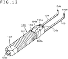
- FIG. 12 is a figure depicting a configuration example of a magnetic core coil disclosed in Patent Document 2.
- a coil 101 is wound around a ferrite core 102 as an example of a magnetic material core
- a terminal leading-out member 103 made of a resin, for example is connected to one end, in the axial direction orthogonal to the winding cross section of the coil 101, of the ferrite core 102, and a pair of metal terminal pieces 104 and 105 are provided for the terminal leading-out member 103.
- the ferrite core 102 is provided in a center position thereof with a through-hole 102a along the axial direction, and has a rod-like (columnar) shape with a flat cross-sectional shape.
- a core body main body portion exclusive of a tip portion (constituting a pen tip) of a core body of the electronic pen is inserted and passed in the through-hole 102a.
- the terminal leading-out member 103 is provided on the opposite side of the ferrite core 102 from the tip portion of the core body, and is used for connection to a circuit board on which an electronic circuit is formed.
- the ferrite core 102 is fitted in a recess provided in the terminal leading-out member 103, and is adhered to the latter with an adhesive, thereby being joined to the terminal leading-out member 103.
- the metal terminal pieces 104 and 105 are fixed on one end side in the terminal leading-out member 103 by resin molding, and have tips 104a and 105a of one-side ends thereof protruding and exposed to the outside of the terminal leading-out member 103, as depicted in FIG. 12 .
- one end 101a of the coil 101 wound around the ferrite core 102 is connected to the tip 104a of the one-side end of the metal terminal piece 104, while the other end 101b of the coil 101 is connected to the tip 105a of the one-side end of the metal terminal piece 105, by soldering, for example.
- the metal terminal pieces 104 and 105 are led out to extend from the terminal leading-out member 103 in the axial direction of the ferrite core 102 toward the side opposite to the ferrite core side, as depicted in FIG. 12 .
- tip portions on the other end side of the metal terminal pieces 104 and 105 are bent portions 104b and 105b which are bent into directions orthogonal to the axial direction, toward the side of the circuit board of the electronic circuit.
- the circuit board is formed with through-holes at positions corresponding to the bent portions 104b and 105b on the other end side of the metal terminal pieces 104 and 105.
- the bent portions 104b and 105b on the other end side of the metal terminal pieces 104 and 105 are inserted into the through-holes of the circuit board and soldered to the latter, whereby the magnetic core coil 100 is electrically connected to the electronic circuit of the circuit board.
- the magnetic core coil 100 in the example of FIG. 12 is produced by a method in which, first, the ferrite core 102 is fixed to the terminal leading-out member 103, and then a wire material is wound by rotating the ferrite core 102 together with the terminal leading-out member 103, thereby winding the coil 101 around the ferrite core 102. Thereafter, one end (for example, the winding starting end) 101a and the other end (for example, the winding ending end) 101b of the coil 101 are soldered respectively to the tip 104a of one-side end of the metal terminal piece 104 and the tip 105a of one-side end of the metal terminal piece 105.
- the magnetic core coil 100 in the example of FIG. 12 mounting of the magnetic core coil 100 to the circuit board is remarkably facilitated, as compared to the case where the terminal leading-out member 103 and the metal terminal pieces 104 and 105 are not used.
- the magnetic core coil 100 provided with the metal terminal pieces 104 and 105 through the terminal leading-out member 103 as aforementioned is used for an electronic pen
- the electronic pen would be increased in size, and be raised in cost, by an extent according to the terminal leading-out member 103.
- the configuration in which the ferrite core 102 is fitted in a recess provide in the terminal leading-out member 103 and adhered to the latter with an adhesive results in that the external shape in the direction orthogonal to the axial direction of the terminal leading-out member 103 is greater than the external shape in the direction orthogonal to the axial direction of the ferrite core 102.
- the tips 104a and 105a on one end side of the metal terminal pieces 104 and 105 are designed to protrude from the terminal leading-out member 103 in the direction orthogonal to the axial direction, for connection of one end and the other end of the coil 101, so that the tips 104a and 105a on one end side of the metal terminal pieces 104 and 105 are also hampering reductions in the size and thickness (radial size) of the magnetic core coil 100.
- the magnetic core coil 100 it is necessary to fix the ferrite core 102 to the terminal leading-out member 103 configured to be equipped with the metal terminal pieces 104 and 105, which leads to a surplus of production steps and an unwanted increase in cost.
- a magnetic core coil according to the present invention is a magnetic core coil having a coil wound around a core formed of a magnetic material, and having two terminal members formed of a conductive material, characterized in that the two terminal members are fixed to the core in a state in which the two terminal members extend from one end, in an axial direction orthogonal to a coil winding cross section, of the core in the axial direction, and a winding starting end and a winding ending end of the coil are electrically connected to those portions of the two terminal members which protrude in the axial direction from the one end of the core.
- an electronic pen is an electronic pen including a magnetic core coil, a pressure detection section, and a circuit board which are disposed in a tubular casing along an axial direction of the casing, characterized in that the magnetic core coil has a coil wound around a core formed of a magnetic material, and has two terminal members, the two terminal members are fixed to the core in a state in which the two terminal members extend from one end, on the circuit board side in an axial direction orthogonal to a coil winding cross section, of the core in the axial direction, a winding starting end and a winding ending end of the coil are electrically connected to those portions of the two terminal members which protrude in the axial direction from the one end of the core, tip portions of the two terminal members are connected to the circuit board in such a manner as to constitute a resonance circuit with a capacitor formed on the circuit board, and the pressure detection section detects a pressure exerted on a tip of a core body which protrudes from one opening of the tubular casing.
- the two terminal members are fixed to the core formed of a magnetic material in a state in which the two terminal members protrude from one end, in an axial direction orthogonal to the coil winding cross section, of the core in the axial direction.
- the two terminal members are fixed to the core directly, without any terminal leading-out member interposed therebetween.
- the winding starting end and the winding ending end of the coil are electrically connected to those portions of the two terminal members which protrude in the axial direction from the one end of the core.
- the two terminal members extended in the axial direction from the one end of the core are connected to a circuit board, thereby being connected to an electronic circuit formed on the circuit board.
- the magnetic core coil according to the present invention has the two terminal members connected directly to the core, the external shape of the magnetic core coil in the direction orthogonal to the axial direction of the core can be made substantially equal to the outside diameter of the core.
- the winding starting end and the winding ending end of the coil are electrically connected to those portions of the two terminal members which protrude in the axial direction from one end of the core, the parts of the connection points also do not protrude in the direction orthogonal to the axial direction of the core; in this point, also, the external shape of the magnetic core coil in the direction orthogonal to the axial direction of the core can be made to be substantially equal to the outside diameter of the core.
- the external shape of the magnetic core coil in the direction orthogonal to the axial direction of the core can be made to be equal to and as thin as the outside diameter of the core. Further, since the terminal leading-out member described in related art example can be omitted, the magnetic core coil can be reduced also in the length (size) in the axial direction.
- the coil is connected directly to the two terminal members without using any terminal leading-out member, the number of production steps is reduced, and the magnetic core coil can be produced at low cost.
- the magnetic core coil is reduced in thickness (radial size) and size, which contributes to reductions in the thickness (radial size) and size of the electronic pen itself.
- the magnetic core coil according to the present invention can be made small in thickness (radial size) and size and can be produced in a reduced number of production steps and at low cost.
- the magnetic core coil is made to be small in thickness (radial size) and size, and, therefore, the electronic pen itself can also be made small in thickness (radial size) and size.
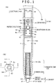
- FIG. 1 depicts figures for explaining a configuration example of the embodiment of an electronic pen according to the present invention, and depicts schematically the whole part of an electronic pen 1 of the present embodiment.
- FIG. 1(A) depicts the inside of the electronic pen 1, by breaking only a case main body 2a of a case 2 (casing) of the electronic pen 1, for explanation.
- FIG. 1(B) is a view of the electronic pen 1 of the present embodiment, as viewed in an axial direction from the side of a core body 4.
- the electronic pen 1 has the case 2 constituting a bottomed tubular casing which is elongated in the axial direction, is opening on one side in the axial direction and is closed on the other side in the axial direction.
- the case 2 is formed, for example, of a resin or the like, and is constituted of a tubular case main body 2a having a cavity therein, and a case cap 2b coupled to the case main body 2a.
- an external shape in a direction orthogonal to the center axis of the case main body 2a is a flat shape, as depicted in FIG. 1(B) .
- the external shape in the direction orthogonal to the center axis of the case main body 2a has two flat surfaces 23 and 24 which are parallel to each other, with the center axis therebetween, as depicted in FIG. 1(B) .
- a cavity inside the case main body 2a also has a cross-sectional shape which is a flat shape according to the external shape of the case main body 2a.
- a core body 4 and a magnetic core coil 5 are accommodated in the state of being connected to a circuit board holder 3 through a pen pressure detection module 7.
- the magnetic core coil 5 is configured by winding a coil 50 around a magnetic material core, in this example, a ferrite core 6, and has terminal members as will be described later.
- the core body 4 includes a core body main body portion 41 composed of a comparatively thin rod-shaped body, and a tip portion 42 formed on one end side in the axial direction of the core body main body portion 41.
- the tip portion 42 of the core body 4 is exposed by protruding to the outside through an opening 21 formed at one end in the axial direction of the case main body 2a, a pen tip being formed at the one end.
- the outside diameter of the tip portion 42 of the core body 4 is, for example, 1 to 2 mm, and the core body main body portion 41 is a cylindrical rod-shaped body smaller than the tip portion 42 in diameter.
- FIG. 2 depicts a configuration example of the ferrite core 6 used for the magnetic core coil 5 of the electronic pen 1 in the present embodiment.
- the ferrite core 6, in this example has a columnar shape provided therein with a through-hole 6a having a diameter R1 slightly greater than a diameter R0 of the core body main body portion 41 of the core body 4, for inserting and passing the core body main body portion 41 through the through-hole 6a.
- the ferrite core 6 has a flat cross-sectional shape corresponding to the cross-sectional shape of the cavity in the case main body 2a.
- FIG. 2(A) is a perspective view of the ferrite core 6 in this example.
- FIG. 2(B) is a top view depicting a state in which the ferrite core 6 in this example is accommodated in the case main body 2a, as viewed in a direction orthogonal to the two flat surfaces 23 and 24 of the external shape of the case main body 2a.
- FIG. 2(C) is a side view depicting a state in which the ferrite core 6 in this example is accommodated in the case main body 2a, as viewed in a direction parallel to the two flat surfaces 23 and 24 of the external shape of the case main body 2a.
- FIG. 2(D) is a view of the ferrite core 6 in this example, as viewed from the core body 4 side in the axial direction. Further, FIG. 2(E) is a sectional view (longitudinal sectional view of the ferrite core 6) taken along line A-A of FIG. 2(B), and FIG. 2(F) is a sectional view (cross-sectional view of the ferrite core 6) taken along line B-B of FIG. 2(C) .
- the ferrite core 6 has a columnar configuration, and has the through-hole 6a with the diameter R1 in a center axis position thereof.
- the external shape of the ferrite core 6 in a direction orthogonal to the center axis is a flat shape according to the profile of the cross section of the case main body 2a, as depicted in FIG. 2(D) .
- the columnar ferrite core 6 has a shape which is provided at side surface portions with flat surfaces 61P and 62P parallel to each other with the center axis therebetween, and in which the two parallel flat surfaces 61P and 62P are connected by curved surfaces 63C and 64C.
- the presence of the curved surfaces 63C and 64C ensures that notwithstanding the ferrite core 6 has the flat shape, the coil 50 can be wound in close contact with the outer surface of the ferrite core 6.
- that end portion in the axial direction of the ferrite core 6 which is on the side of the tip portion 42 of the core body 4 when the core body 4 is inserted and passed through the through-hole 6a is formed with a tapered portion 65 tapered toward the side of the tip portion 42 of the core body 4.
- the ferrite core has a flat shape
- an end face of the ferrite core may spread transversely, and it may be difficult to concentrate a magnetic flux into the tip portion 42 of the core body 4, as compared to the case where the end face is true circular as in related art.
- the end portion on the tip portion 42 side of the core body 4 has the tapered portion 65, and the tapered portion 65 is configured such as to be terminated with an annular flat surface 67; therefore, the magnetic flux can be concentrated into the annular flat surface 67 and, hence, the magnetic flux can be concentrated into the tip portion 42 of the core body 4.
- one of the flat surfaces 61P and 62P of the ferrite core 6, in this example, the flat surface 61P, is formed with two grooves 68 and 69 parallel to each other and along the axial direction of the ferrite core 6.
- the two grooves 68 and 69 are formed to extend over the whole length in the axial direction of the ferrite core 6, as depicted in FIGS. 2(A) and (B) .
- two terminal members 51 and 52 are fitted in the two grooves 68 and 69.
- the two grooves 68 and 69 are an example of thin linear recesses for fitting the two terminal members 51 and 52 therein, and their cross-sectional shape (groove shape) may be any of various shapes such as an arcuate shape, a V shape, and a U shape.
- the two terminal members 51 and 52 are rectilinear members composed of thin bar-shaped members or thin plate-shaped members formed of a conductive material, for example, a conductive metal.
- the terminal members 51 and 52 are each configured as an integral body of a conductive metal; in this example, for convenience of explanation, the terminal members 51 and 52 have core connecting portions 51a and 52a, extension portions 51b and 52b, and bent portions 51t and 52t, as part names.
- the terminal members 51 and 52 have their core connecting portions 51a and 52a fitted in the grooves 68 and 69 of the ferrite core 6, and joined to the ferrite core 6 by adhesion with an adhesive, for example.
- the extension portions 51b and 52b of the terminal members 51 and 52 extend in the axial direction from that end portion of the ferrite core 6 at which the tapered portion 65 is not formed. Further, tips of the extension portions 51b and 52b of the terminal members 51 and 52 are bent at a predetermined angle, for example, at a right angle, to the side of an extension surface of the flat surface 62P of the ferrite core 6, whereby bent portions 51t and 52t are formed. Tips of the bent portions 51t and 52t serve as end portions for connection with an electronic circuit of the printed circuit board as will be described later.
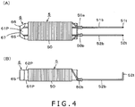
- a litz wire for example, is wound around the ferrite core 6 to form the coil 50, as depicted in FIGS. 4(A) and (B) . Therefore, the terminal members 51 and 52 are not only fitted in the grooves 68 and 69 of the ferrite core 6 and adhered to the ferrite core 6 but also joined to the ferrite core 6 in the manner of being bound to the ferrite core 6 by the wound portion of the coil 50; accordingly, the terminal members 51 and 52 are firmly fixed to the ferrite core 6.
- a winding starting end 50a of the coil 50 is wound multiple times around that part of the extension portion 51b of the terminal member 51 protruding in the axial direction from an end portion of the ferrite core 6 which is in the vicinity of the end portion of the ferrite core 6, and the winding starting end 50a is soldered to the extension portion 51b of the terminal member 51.
- a winding ending end 50b of the coil 50 is wound multiple times around that part of the extension portion 52b of the terminal member 52 protruding in the axial direction from the end portion of the ferrite core 6 which is in the vicinity of the end portion of the ferrite core 6, and the winding ending end 50b is soldered to the extension portion 52b of the terminal member 52. In this way, the magnetic core coil 5 is manufactured.
- a method for winding the coil 50 around the ferrite core 6 there may be mentioned two methods, namely, a method in which the ferrite core 6 side is fixed and the coil 50 is wound around the ferrite core 6, and a method in which the coil 50 is wound around the ferrite core 6 by rotating the ferrite core 6 side, and either of the two methods may be used.
- a step of winding the coil 50 around the ferrite core 6, inclusive of steps of winding the winding starting end 50a and the winding ending end 50b of the coil 50 around the extension portions 51b and 52b of the terminal members 51 and 52 can be carried out using an automatic machine.
- a delivery nozzle for a litz wire for constituting the coil 50 is rotated about the extension portion 51b of the terminal member 51, whereby the winding starting end 50a of the coil 50 is wound around the extension portion 51b, after which the litz wire delivery nozzle is rotated about the ferrite core 6 to wind the coil 50 around the ferrite coil 6, and thereafter the litz wire delivery nozzle is rotated about the extension portion 52b of the terminal member 52, whereby the winding starting end 50a of the coil 50 is wound around the extension portion 52b.
- the ferrite core 6 is rotated with the extension direction position of the terminal member 51 as a rotational axis position, whereby the litz wire is wound around the extension portion 51b of the terminal member 51 as the winding starting end 50a of the coil 50.
- the ferrite core 6 is rotated with the center line position of the ferrite core 6 as the rotational axis position, to wind the litz wire around the ferrite core 6.
- the ferrite core 6 is rotated with the extension direction position of the terminal member 52 as the rotational axis position, to wind the litz wire around the extension portion 52b of the terminal member 52 as the winding ending end 50b of the coil 50.
- the winding starting end 50a of the coil 50 wound around the extension portion 51b of the terminal member 51 and the winding ending end 50b of the coil 50 wound around the extension portion 52b of the terminal member 52 are soldered to the terminal member 51 and the terminal member 52, respectively, to be thereby electrically connected to the terminal members 51 and 52.
- the extension portions 51b and 52b of the terminal members 51 and 52 may be formed, at positions in the vicinity of the end portion of the ferrite core 6, with projections 51c and 52c such as to form wedge shapes (V-shaped grooves) between themselves and the extension portions 51b and 52b.
- the litz wire for constituting the coil 50 is engaged with the wedge shapes (V-shaped grooves) between the projections 51c and 52c and the extension portions 51b and 52b, the litz wire can be easily locked to the terminal members 51 and 52.
- that portion of the ferrite core 6 around which the coil 50 is wound may be set lower in height than other portions such that stepped portions 6b and 6c are formed at both ends of the portion around which the coil 50 is wound. This ensures that the litz wire to be wound around the ferrite core 6 as the coil 50 can be easily wound in a well aligned manner, with the stepped portions 6b and 6c as guides.
- the ferrite core 6 may be formed with thin annular projections 6d and 6e having a height comparable to the thickness of the litz wire of the coil 50.
- the terminal members 51 and 52 can be easily fitted into the ferrite core 6, as follows. Specifically, two linear bodies of a conductive metal constituting the terminal members 51 and 52 are laid on rails, with a spacing therebetween corresponding to the spacing between the two grooves 68 and 69 of the ferrite core 6. Then, a plurality of ferrite cores 6 are pressed from above the two linear bodies of the conductive metal, such as to fit the linear bodies of the conductive metal into the two grooves 68 and 69, at an interval set taking into account the extension portions 51b and 52b and the bent portions 51t and 52t, whereby the linear bodies of the conductive metal are gradually joined to the ferrite cores 6 individually.
- an adhesive is preliminarily applied to the grooves 68 and 69, and the terminal portions 51 and 52 are attached to the grooves 68 and 69. Then, the two linear bodies of the conductive metal are cut at intervals set taking into account the lengths in the axial direction of the ferrite core 6, the extension portions 51b and 52b, and the bent portions 51t and 52t.
- the coil 50 is wound around the ferrite core 6, both ends of the coil 50 are soldered to the terminal members 51 and 52, and thereafter the bent portions 51t and 52t are formed. Note that, naturally, the bent portions 51t and 52t may be formed before winding the coil 50 around the ferrite core 6.
- the magnetic core coil 5 configured as above-mentioned is provided on the most opening 21 side in the cavity of the case main body 2a of the electronic pen 1, as depicted in FIG. 1(A) .
- the circuit board holder 3 for holding the printed circuit board 8 is disposed on the opposite side of the magnetic core coil 5 from the opening 21, through the pen pressure detection module 7.
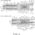
- FIG. 6(A) is a sectional view taken along line X-X of FIG. 1(B) , and is a sectional view of an essential part when the electronic pen 1 is cut in a direction which passes the axial center position of the electronic pen 1 and which is parallel to the two flat surfaces 23 and 24 (see FIG. 1(B) ) of the external shape of the case main body 2a.
- FIG. 6(B) is a sectional view taken along line Y-Y of FIG. 1(B) , and is a sectional view of an essential part when the electronic pen 1 is cut in a direction which passes the axial center position of the electronic pen 1 and which is perpendicular to the two flat surfaces 23 and 24.
- the cavity of the case main body 2a has a diameter greater than the diameter of the opening 21, and an inner wall surface constituting the cavity is formed with a stepped portion 22 on the opening 21 side.
- a tip side of the tapered portion 65 of the ferrite core 6 of the magnetic core coil 5 abuts on the stepped portion 22, such that the magnetic core coil 5 does not slip off from the cavity of the case main body 2a to the outside.
- the core body 4 is inserted and passed through the through-hole 6a (see FIG. 2 ) of the ferrite core 6 and engaged with the pen pressure detection module 7.
- the core body 4 is formed of a rigid material, examples of which include polycarbonate, synthetic resin, and acrylonitrile-butadienestyrene (ABS) resin.
- the circuit board holder 3 is formed of a resin, for example, and is provided with a printed circuit board mount base portion 3a in a longitudinal direction which coincides with the axial direction of the electronic pen 1 when accommodated in the cavity of the case main body 2a.
- the printed circuit board 8 is mounted on the printed circuit board mount base portion 3a of the circuit board holder 3.
- the printed circuit board 8 has an elongated rectangular shape having a width narrower than the inside diameter of the case main body 2a and a predetermined length in the longitudinal direction.
- the length in the longitudinal direction of a circuit board mount surface of the printed circuit board mount base portion 3a is substantially equal to or slightly greater than the length in the longitudinal direction of the printed circuit board 8.
- the length in the transverse direction of the circuit board mount surface of the printed circuit board mount base portion 3a is selected to be slightly larger than the width of the printed circuit board 8.
- the printed circuit board 8 is provided with a push switch (side switch) 11 which is turned ON when depressed and returns to be OFF when the depression is stopped.
- the printed circuit board 8 is provided also with capacitors 12 and 13 which constitute a resonance circuit together with an inductance element composed of the coil 50 wound around the ferrite core 6.
- the capacitor 12 is a trimmer capacitor of which capacitance can be regulated.
- the printed circuit board 8 is formed with other circuit component parts and conductor patterns which are not depicted in the drawings. Note that to the resonance circuit, a capacitance Cd constituted of a semiconductor chip 80 of the pen pressure detection module 7 to be described later is also connected, in parallel to the inductance element.
- a side circumferential surface of the case main body 2a of the electronic pen 1 is formed with a through-hole (omitted in the drawing) at a position corresponding to the side switch 11, and a depression operating piece 16 (see FIG. 1(B) ) for the side switch 11 is exposed such that the side switch 11 can be thereby depressed through the through-hole.
- a predetermined function is allocated and set, on the side of an electronic apparatus provided with a position detecting device 200 described later, to the depressing operation of the side switch 11 by the depression operating piece 16.
- the depressing operation of the side switch 11 by the depression operating piece 16 can be set to be allocated as an operation equivalent to a click operation of a pointing device such as a mouse.
- the capacitors 12 and 13 constituting part of the resonance circuit are disposed in the printed circuit board 8 as chip parts.
- the capacitance of the trimmer capacitor 12 is regulated, whereby the resonance frequency of the resonance circuit is controlled.
- a wall portion 31 arranged in a direction orthogonal to the printed circuit board mount base portion 3a of the printed circuit holder 3 is formed at an end portion on the core body 4 side in the longitudinal direction of the printed circuit board mount base portion 3a.
- the circuit board holder 3 has the part of the wall portion 31 as one end in the longitudinal direction, and a surface on the core body 4 side of the wall portion 31 is a flat surface.
- a locking portion 32 by which an end portion in the longitudinal direction of the printed circuit board 8 is locked to the printed circuit board mount base portion 3a of the circuit board holder 3 by clamping the printed circuit board 8 in the thickness direction is formed at that end portion in the longitudinal direction of the printed circuit board mount base portion 3a which is on the side opposite to the core body 4 side.
- the pen pressure detection module 7 is provided between the wall portion 31 of the circuit board holder 3 and the ferrite core 6 around which the coil 50 is wound.
- that end face of the pen pressure detection module 7 which is on the side opposite to the core body 4 side is a flat surface, and is in the state of abutment on the surface of the wall portion 31 of the circuit board holder 3.
- metal terminal pieces 71a and 71b (see FIG. 6(B) and FIGS. 7(A) and (B) described later) led out in the axial direction from a pressure sensing device 71 held by the pen pressure detection module 7 are soldered at soldered portions 8b and 8c, in the vicinity of the wall portion 31 on the core body 4 side in the longitudinal direction of the printed circuit board mount base portion 3a of the circuit board holder 3, whereby the pen pressure detection module 7 is fixed to the circuit board holder 3.
- the metal terminal pieces 71a and 71b are led out from the pressure sensing device 71 in the axial direction of the cavity of the case main body 2a, and tip sides thereof are bent toward the printed circuit board 8 in a direction orthogonal to the axial direction.
- through-holes are formed at positions of the soldered portions 8b and 8c of the printed circuit board 8, and the printed circuit board mount base portion 3a of the circuit board holder 3 is formed with through-holes at the corresponding positions.
- the bent portions of the tip portions of the metal terminal pieces 71a and 71b of the pen pressure detection module 7 are inserted through the through-holes in the printed circuit board mount base portion 3a and the through-holes in the printed circuit board 8, from the back side of the printed circuit board mount base portion 3a, to protrude to the circuit board surface 8a side of the printed circuit board 8.
- the tip portions of the metal terminal pieces 71a and 71b thus protruding to the circuit board surface 8a side of the printed circuit board 8 are soldered, whereby the soldered portions 8b and 8c are formed.
- soldered portions 8b and 8c electrical connection between circuit component parts of the printed circuit board 8 and a pressure sensing portion of the pressure sensing device 71 is conducted.
- soldering at the soldered portions 8b and 8c is conducted, whereby the pen pressure detection module 7 is fixed to the circuit board holder 3.
- the side of the pen pressure detection module 7 opposite to its portion of connection with the circuit board holder 3 is in abutment on the end face side where the terminal members 51 and 52 of the ferrite core 6 of the magnetic core coil 5 protrude in the axial direction.
- Part of the ferrite core 6 may be fitted to the pen pressure detection module 7.
- the two terminal members 51 and 52 connected to the ferrite core 6 in such a manner as to protrude and extend in the axial direction from that end face of the ferrite core 6 which abuts on the pen pressure detection module 7 have the extension portions 51b and 52b extending along an outside surface of the pen pressure detection module 7 to the position of the printed circuit board 8 of the circuit board holder 3.
- the tips of the bent portions 51t and 52t of the terminal members 51 and 52 are inserted into the through-holes formed in the printed circuit board 8, to protrude to the circuit board surface 8a side of the printed circuit board 8.
- the tip portions of the bent portions 51t and 52t of the terminal members 51 and 52 protruding to the circuit board surface 8a side of the printed circuit board 8 are soldered, whereby soldered portions 8d and 8e are formed.
- soldered portions 8d and 8e By the soldered portions 8d and 8e, the capacitors 12 and 13 of the printed circuit board 8 and the coil 50 of the magnetic core coil 5 are connected in parallel, whereby electrical connection such as to form a resonance circuit is performed; in addition, in a state in which the pen pressure detection module 7 is held between the magnetic core coil 5 and the circuit board holder 3, soldering is conducted at the soldered portions 8d and 8e, whereby the magnetic core coil 5 is fixed to the circuit board holder 3.
- the printed circuit board 8 in a state in which the printed circuit board 8 is locked to the printed circuit board mount base portion 3a by the locking portion 32 and is fixed by the soldered portions 8b, 8c, 8d, and 8e, the printed circuit board 8 does not contact the inner wall surface of the case main body 2a but is spaced from the case main body 2a.
- the circuit board holder 3 is connected to a case cap 2b at a connection portion 3c at that end portion of the printed circuit board mount base portion 3a which is on the side opposite to the core body 4 side in the longitudinal direction, so that the case cap 2b and the circuit board holder 3 can be handled as an integral body.
- a structure in which the printed circuit board 8 is mounted on and fixed to the printed circuit board mount base portion 3a of the circuit board holder 3 and in which the pen pressure detection module 7 and the magnetic core coil 5 are fixed and held on the circuit board holder 3 can be handled as a single module part (referred to as pen module part).
- the pen module part is accommodated in the cavity of the case main body 2a, the core body 4 is inserted through the opening 21 of the case main body 2a, and the pen pressure detection module 7 is engaged through the through-hole 6a of the ferrite core 6 and a through-hole 9b of a terminal leading-out member 9, whereby the electronic pen 1 can be completed.
- the circuit board holder 3 is locked within the cavity of the case body 2a in such a manner as not to move in the axial direction.
- the pen pressure detection module 7 fixed to the circuit board holder 3, the pen pressure detection module 7 is also locked within the cavity of the case main body 2a in such a manner as not to move in the axial direction, and a pen pressure exerted on the core body 4 can be received.
- the circuit board holder 3 is connected to the case cap 2b in such a manner that the center line position in the axial direction of the pen pressure detection module 7 and the center line position in the axial direction of the magnetic core coil 5 coincide with the center line position in the axial direction of the cavity of the case main body 2a.
- the pen pressure detection module 7 includes the pressure sensing device 71, an outer holder 72 as a first holder, and an inner holder 73 as a second holder.
- the outer holder 72 is formed of a rigid resin, for example, polyoxymethylene (POM) (or polyacetal) resin or polycarbonate.
- the outer holder 72 has a tubular shape, and accommodates in its cavity 72a the pressure sensing device 71 and the inner holder 73 in the state of being aligned in the axial direction.
- the inner holder 73 includes a locking member 731 as an example of a first member for locking the core main body portion 41 of the core body 4 to the inner holder 73 by engaging with the core body main body portion 41, and a pressing member 732 as an example of a second member for transmitting the pressure exerted on the core body 4 to the pressure sensing device 71 by contacting the pressure sensing device 71 as will be described later.
- the locking member 731 is formed, in the axial direction in a central portion on the core body main body portion 41 side in the axial direction thereof, with a recessed hole 731a into which the core body main body portion 41 is inserted.
- the recessed hole 731a has a cylindrical shape, and is formed at an inner wall surface thereof with an annular projection 731b projecting in an arcuate shape.
- the core body main body portion 41 is formed, at a predetermined position of an end portion thereof and in a direction orthogonal to the axial direction thereof, with an annular projection 411 projecting in an arcuate shape, in this example.
- the core body main body portion 41 is inserted into the recessed hole 731a in the locking member 731 of the inner holder 73 through a through-hole 72b in the outer holder 72.
- an end face of the core body main body portion 41 abuts on a bottom portion of the recessed hole 731a.
- the core body main body portion 41 is locked in the recessed hole 731a of the locking member 731 by the engagement between the annular projection 731b and the annular projection 411.
- the core body main body portion 41 is kept in the state of being locked in the recessed hole 731a of the locking member 731, unless the core body main body portion 41 is drawn out with a predetermined force.
- the pressing member 732 as an example of the second member of the inner holder 73 is composed of an elastic member, in the present embodiment.
- the pressing member 732 is formed on that side of the locking member 731 which is for facing the pressure sensing device 71 in the axial direction, in the state of being connected to the locking member 731.
- the pressing member 732 is formed, at an end face in the axial direction thereof, with a projection in the shape of projecting from the end face, in this example, a small-diameter cylindrical projection 732a.
- the end face of the cylindrical projection 732a of the pressing member 732 faces the pressure sensing device 71 side, and is in the state of being able to contact the pressure sensing device 71.
- FIG. 7 depicts figures for explaining the pressure sensing device 71 in this example.
- the pressure sensing device 71 in the present embodiment includes the semiconductor chip 80 constituting a pressure sensing portion of a capacitance system, and a socket 710 which accommodates the semiconductor chip 80 therein and which is provided with the above-mentioned metal terminal pieces 71a and 71b.
- the semiconductor chip 80 is accommodated in an accommodating recess 711 of the socket 710, whereby a first electrode 81 and a second electrode 82 which will be described later are individually connected to the metal terminal pieces 71a and 71b.
- FIG.7(C) depicts a cross section of the semiconductor chip 80.
- FIG. 7(D) is a plan view of the semiconductor chip 80, as viewed in a direction of exerting a pressure P depicted in FIG. 7(C).
- FIG. 7(C) is a sectional view taken along line C-C of FIG. 7(D) .
- the semiconductor chip 80 in this example is for detecting an exerted pressure as a variation in capacitance, and, in this example, it is configured as depicted in FIG. 7(C) .
- the semiconductor chip 80 in this example has a rectangular parallelepiped shape having, for example, lengths L in the longitudinal and transverse direction of 1.5 mm and a height H of 0.5 mm.
- the semiconductor chip 80 in this example includes the first electrode 81, the second electrode 82, and an insulating layer (dielectric layer) 83 between the first electrode 81 and the second electrode 82.
- the first electrode 81 and the second electrode 82 are formed of a conductor composed of single crystal silicon (Si).
- the insulating layer 83 is formed, on the side of its surface facing the first electrode 81, with a recess 84 which has a circular shape with a central position of the surface as a center. Due to the recess 84, a space 85 is formed between the insulating layer 83 and the first electrode 81. Due to the presence of the space 85, the first electrode 81 can be displaced in the manner of bending toward the space 85 when pressed from the side of an upper surface 81a which is on the side opposite to its surface facing the second electrode 82.
- a capacitance Cd is formed between the first electrode 81 and the second electrode 82.
- the first electrode 81 is displaced in the manner of bending toward the space 85 side, whereby the spacing between the first electrode 81 and the second electrode 82 is shortened, and the capacitance Cd varies in the manner of increasing in value.
- the locking member 731 of the inner holder 73 in engagement with the core body main body portion 41 of the core body 4, in the pen pressure detection module 7, is displaced within the outer holder 72 toward the side of the semiconductor chip 80 of the pressure sensing device 71 in the axial direction according to the pen pressure exerted. Therefore, the pressing member 732 fitted to the locking member 731 causes the first electrode 81 of the semiconductor chip 80 of the pressure sensing device 71 to bend toward the second electrode 82 side through the space 85, whereby the capacitance Cd of the capacitor configured between the first electrode 81 and the second electrode 82 of the semiconductor chip 80 is varied according to the pen pressure. Due to the variation in the capacitance Cd, the resonance frequency of the resonance circuit of the electronic pen 1 is varied, and, by detecting the variation in the resonance frequency, the position detecting device detects the pen pressure exerted on the core body 4 of the electronic pen 1.
- FIG. 8 is a block diagram depicting a circuit configuration example of the position detecting device 200 in this example.
- the electronic pen 1 has a resonance circuit including the coil 50, the capacitors 12 and 13, and a capacitor (capacitance Cd) constituted of the semiconductor chip 80.
- the coil 50 as an inductance element
- the capacitor (capacitance Cd) constituted of the semiconductor chip 80 are connected in parallel, and, further, a series circuit of the side switch 11 and the capacitor 13 constituted of a chip part is connected in parallel.
- the connection of the capacitor 13 to the parallel resonance circuit is controlled, and resonance frequency is varied.
- the capacitance Cd of the capacitor (capacitance Cd) constituted of the semiconductor chip 80 varies according to the pen pressure exerted, so that the resonance frequency varies according to the pen pressure.
- the position detecting device 200 detects a variation in the phase of a signal from the electronic pen 1, to detect a variation in the frequency, thereby detecting whether or not the side switch 11 has been depressed and detecting the pen pressure exerted on the core body 4 of the electronic pen 1.
- an X-axis direction loop coil group 211 and a Y-axis direction loop coil group 212 are stacked to form position detection coils 210.
- the position detecting device 200 is provided with a selection circuit 213 to which the X-axis direction loop coil group 211 and the Y-axis direction loop coil group 212 are connected.
- the selection circuit 212 sequentially selects the loop coils in one of the two loop coil groups 211 and 212.
- the position detecting device 200 is provided with an oscillator 231, a current driver 232, a switching connection circuit 233, a reception amplifier 234, a detector 235, a low pass filter 236, a sample hold circuit 237, an analog to digital (A/D) conversion circuit 238, a synchronous detector 239, a low pass filter 240, a sample hold circuit 241, an A/D conversion circuit 242, and a process control unit 243.
- the process control unit 243 is composed of a microcomputer.
- the oscillator 231 generates an alternate current (AC) signal of a frequency f0.
- the oscillator 231 supplies the thus generated AC signal to the current driver 232 and the synchronous detector 239.
- the current driver 232 converts the AC signal supplied from the oscillator 231 into a current, and sends the current to the switching connection circuit 233.
- the switching connection circuit 233 switches a connection destination (a transmission-side terminal T or a reception-side terminal R) to which the loop coil selected by the selection circuit 213 is to be connected, under the control by the process control unit 243.
- the connection destinations are configured such that the current driver 232 is connected to the transmission-side terminal T, whereas the reception amplifier 234 is connected to the reception-side terminal R.
- An induction voltage generated in the loop coil selected by the selection circuit 213 is sent to the reception amplifier 234 through the selection circuit 213 and the switching connection circuit 233.
- the reception amplifier 234 amplifies the induction voltage supplied from the loop coil, and sends the amplified induction voltage to the detector 235 and the synchronous detector 239.
- the detector 235 detects the induction voltage generated in the loop coil, or the received signal, and sends the detected signal to the low pass filter 236.
- the sample hold circuit 237 holds a voltage value of an output signal of the low pass filter 236 at a predetermined timing, specifically, a predetermined timing during a reception period, and sends the voltage value to the A/D conversion circuit 238.
- the A/D conversion circuit 238 converts an analog output of the sample hold circuit 237 into a digital signal, and outputs the digital signal to the process control unit 243.
- the synchronous detector 239 performs synchronous detection of an output signal of the reception amplifier 234 with an AC signal from the oscillator 231, and sends to the low pass filter 240 a signal at a level according to a phase difference between the output signal and the AC signal.
- the low pass filter 240 which has a cutoff frequency sufficiently lower than the frequency f0, converts an output signal of the synchronous detector 239 into a DC signal, and sends the DC signal to the sample hold circuit 241.
- the sample hold circuit 241 holds a voltage value of an output signal of the low pass filter 240 at a predetermined timing, and sends the voltage value to the A/D conversion circuit 242.
- the A/D conversion circuit 242 converts an analog output of the sample hold circuit 241 into a digital signal, and outputs the digital signal to the process control unit 243.
- the process control unit 243 controls each section of the position detecting device 200. Specifically, the process control unit 243 controls the loop coil selection in the selection circuit 213, the switching in the switching connection circuit 233, and the timings in the sample hold circuits 237 and 241. Based on input signals from the A/D conversion circuits 238 and 242, the process control unit 243 transmits an electromagnetic wave from the X-axis direction loop coil group 211 and the Y-axis direction loop coil group 212 with a predetermined transmission continuation time.
- an induction voltage is generated by the electromagnetic wave transmitted from the electronic pen 1.
- the process control unit 243 calculates coordinate values of an indicated position in an X-axis direction and a Y-axis direction of the electronic pen 1.
- the process control unit 243 detects whether or not the side switch 11 has been depressed and also detects the pen pressure.
- the position of the electronic pen 1 coming near can be detected by the process control unit 243. Moreover, by detecting the phase (frequency shift) of the received signal, it is possible, in the electronic pen 1, to detect whether or not the depression operating piece 16 of the side switch 11 has been depressed, and to detect the pen pressure exerted on the core body 4 of the electronic pen 1.
- the two terminal members 51 and 52 are fixed directly to the ferrite core 6, so that the external shape of the magnetic core coil 5 in the direction orthogonal to the axial direction of the ferrite core 6 can be made to be substantially equal to the outside diameter of the ferrite core 6.
- the winding starting end 50a and the winding ending end 50b of the coil 50 are electrically connected at those portions of the two terminal members 51 and 52 which protrude in the axial direction from one end of the ferrite core 6. Therefore, the portions of the connection points also do not protrude in the direction orthogonal to the axial direction of the ferrite core 6.
- the external shape of the magnetic core coil 5 in the direction orthogonal to the axial direction of the ferrite core 6 can be made to be substantially equal to the outside diameter of the ferrite core 6.
- the external shape of the magnetic core coil 5 in the direction orthogonal to the axial direction of the ferrite core 6 can be made to be thin (small in radial size) in the same manner as the outside diameter of the core. Further, since the terminal leading-out members described in the related art example can be omitted, the length (size) in the axial direction can also be reduced.
- the ends 50a and 50b of the coil 50 are connected directly to the two terminal members 51 and 52, without using any terminal leading-out member, the number of manufacturing steps is reduced, and manufacturing cost can be reduced. Besides, direct connection to the printed circuit board 8 can be achieved by the two terminal members 51 and 52, and, in this point, also, the number of production steps is reduced.
- the two terminal members 51 and 52 are connected directly to the ferrite core 6, without using any terminal leading-out member. Therefore, there are effects that measurement of coil constants such as the inductance value of the magnetic core coil 5 alone is facilitated, and accuracy in management of the coil constants can be enhanced.
- the magnetic core coil is thin (small in radial size) and small in size, which contributes to reductions in the thickness and size of the electronic pen itself.
- the two terminal members 51 and 52 are formed at one flat surface 61P of the two opposed flat surfaces 61P and 62P of the flat ferrite core 6, and the core connecting portions 51a and 52a of the terminal members 51 and 52 have lengths corresponding substantially to the whole length in the axial direction of the ferrite core 6.
- the manner in which the two terminal members 51 and 52 are connected to the ferrite core 6 is not limited to that in the above example.
- FIGS. 9(A) to (E) depict other configuration examples of the manner in which the two terminal members 51 and 52 are connected to the ferrite core 6 of the magnetic core coil 5, and each depict a state before winding of the coil 50.
- Each of FIGS. 9(A) to (E) depicts four views of the magnetic core coil 5.
- the two views on the left side are views of the flat ferrite core 6 as viewed in the axial direction from the side where the tapered portion 65 is formed, whereas the two views on the right side are views as viewed from a direction orthogonal to the axial direction.
- FIGS. 9(A) to (E) depict other configuration examples of the manner in which the two terminal members 51 and 52 are connected to the ferrite core 6 of the magnetic core coil 5, and each depict a state before winding of the coil 50.
- Each of FIGS. 9(A) to (E) depicts four views of the magnetic core coil 5.
- the two views on the left side are views of the flat ferrite core 6 as viewed in the
- the two views on the upper side are views in the case where the flat surfaces 61P and 62P are set horizontal, whereas the two views on the lower side are views in the case where the flat surfaces 61P and 62P are set vertical.
- the terminal members 51 and 52 are joined with their core connecting portions 51Aa and 52Aa fitted in two grooves 68A and 69A provided on the flat surface 61P side of the ferrite core 6, in the same manner as in the example of the above embodiment.
- the length in the axial direction of the grooves 68A and 69A is set to be shorter than the length in the axial direction of the ferrite core 6, for example, to be not more than 1/2 times the length in the axial direction of the ferrite core 6.
- the other points are the same as in the example of the above embodiment.
- grooves 68B and 69B in which to fit core connecting portions 51Ba and 52Ba of terminal members 51B and 52B are provided to extend over substantially the whole length in the axial direction of the ferrite core 6, in substantially central positions of curved surfaces 63C and 64C of the ferrite core 6.
- extension portions 51Bb and 52Bb of the terminal members 51B and 52B are formed at tip portions thereof with bent portions 51Bt and 52Bt which are bent into directions orthogonal to the axial direction such as to come closer to each other.
- bent portions 51Bt and 52Bt in the case of this example are formed to extend in the direction parallel to a circuit board surface of the printed circuit board up to positions above the circuit board surface of the printed circuit board, whereby soldering can be performed at the circuit board surface of the printed circuit board.
- the length in the axial direction of grooves 68C and 69C formed in curved surfaces 63C and 64C of the ferrite core 6 is set to be shorter than, for example, to be not more than 1/2 times of the whole length of, the grooves 68B and 69B formed in the curved surfaces 63C and 64C of the ferrite core 6 in the case of the example of FIG. 9(B) .
- the length of core connecting portions 51Ca and 52Ca of terminal members 51C and 52C are also set according to the length in the axial direction of the grooves 68C and 69C.
- the other points of configuration of the magnetic core coil 5c in the example of FIG. 9(C) are the same as those of the magnetic core coil 5B in the example of FIG. 9(B) .
- the grooves for the two terminal members are formed in the outside surface of the ferrite core 6.
- a configuration may be adopted in which through-holes for the terminal members are formed in the axial direction of the ferrite core 6, and the terminal members are fitted in the through-holes, whereby the terminal members are fitted and fixed to the ferrite core 6.
- FIG. 9(D) depicts an example of such a case.
- two through-holes 68D and 69D are formed to extend over substantially the whole length in the axial direction of the ferrite core 6, in such a manner as to be partly connected to an inner wall surface of the through-hole 6a of the ferrite core 6 in which the core body 4 is inserted and passed.
- the two through-holes 68D and 69D are provided at positions on opposite sides of a center position of the through-hole 6a, in a plane which contains the center line of the through-hole 6a and which is parallel to the flat surfaces 61P and 62P.
- core connecting portions 51Da and 52Da of two terminal members 51D and 52D are formed in such a shape as to be fitted to the through-holes 68D and 69D, and are, for example, press fitted into the through-holes 68D and 69D, thereby being fixed to the ferrite core 6.
- the fitting portions for the core connecting portions 51Da and 52Da of the two terminal members 51D and 52D may be a part in the axial direction, like in the example of FIG. 9(C) ; in that case, they are not through-holes but are fitting holes.
- the magnitude of a magnetic flux when a current flows through the coil 50 is smaller in the vicinity of the center line position of the ferrite core 6, or the through-hole 6a, than on the outer circumferential side surface side. Therefore, where the positions of the connecting portions 51Da and 52Da of the terminal members 51D and 52D are set in the vicinity of the through-hole 6a, the influence on the magnetic flux path can be thereby reduced, so that the lowering in the strength of electromagnetic coupling between the electronic pen 1 and the position detecting device can be suppressed.
- the through-holes in which to fit the two terminal members to thereby fix the terminal members may not be formed to be partly connected to the through-hole 6a as in the example of FIG. 9(D) , but may be formed quite independently from the through-hole 6a of the ferrite core 6.
- FIG. 9(E) depicts an example of such a case.
- two fitting holes 68E and 69E are formed in a part in the axial direction of the ferrite core 6, quite independently from the through-hole 6a of the ferrite core 6 in which the core body 4 is to be inserted and passed.
- the two fitting holes 68E and 69E are provided at positions on opposite sides of a center position of the through-hole 6a, in a plane which contains the center line of the through-hole 6a and which is parallel to the flat surfaces 61P and 62P.
- core connecting portions 51Da and 52Da of the two terminal members 51D and 52D have a shape and a length such as to be fitted to the fitting holes 68E and 69E, and they are, for example, press fitted into the fitting holes 68E and 69E, thereby being fixed to the ferrite core 6.
- the fitting holes 68E and 69E are extended to form through-holes over the whole length in the axial direction of the ferrite core 6, the length of the core connecting portions 51Ea and 52Ea of the two terminal members 51E and 52E are also set to the corresponding length, and the core connecting portions 51Ea and 52Ea are fitted to the through-holes.
- the cross-sectional shape of the ferrite core of the magnetic core coil has been a flat shape in the above embodiment, the cross-sectional shape of the magnetic material core of the magnetic core coil according to the present invention may be any shape.
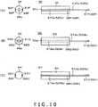
- FIGS. 10(A) and (B) depict an example of a magnetic core coil 5F in the case where the cross-sectional shape of a ferrite core 6F as an example of the magnetic material core is a circle.
- the views on the left side are views of the ferrite core 6F as viewed in the axial direction from the insertion side of the core body, whereas the views on the right side are views of the ferrite core 6F as viewed from a direction orthogonal to the axial direction.
- the magnetic core coil 5F in the example of FIG. 10(A) has a configuration in which the ferrite core 6F circular in cross section is formed with a through-hole 6Fa in which to insert a core body, and two grooves 68F and 69F extending over the whole part in the axial direction are formed in a side circumferential surface at positions spaced by an angular interval of 180 degrees from each other.
- core connecting portions 51Fa and 52Fa of two terminal members 51F and 52F are fitted in the two grooves 68F and 69F of the ferrite core 6F, and are joined thereto with an adhesive, for example.
- the terminal members 51F and 52F are fixed to the ferrite core 6 in a state in which extension portions 51Fb and 52Fb of the terminal members 51F and 52F extend protruding in the axial direction of the ferrite core 6F.
- FIG. 10(A) corresponds to the example of FIG. 9(B)
- a configuration may be adopted in which the length of the parts where the ferrite core 6 and the terminal members 51F and 52F are connected is shorter than the length in the axial direction of the ferrite core 6, such as to correspond to the example of FIG. 9(C) .
- a ferrite core 6G circular in cross section is formed with a through-hole 6Ga in which to insert a core body, and two grooves 68G and 69G partly connected to the through-hole 6Ga are formed in the axial direction, in the same manner as in the example of FIG. 9(D) .
- core connecting portions 51Da and 52Da of two terminal members 51D and 52D have a shape and a length such as to fit to fitting holes 68D and 69D, and are, for example, press fitted into the fitting holes 68D and 69D, thereby being fixed to the ferrite core 6G.
- the length of parts where the ferrite core 6G and the terminal members 51G and 52G are connected may be shorter than the length in the axial direction of the ferrite core 6G.
- the magnetic material core is provided with the through-hole in which to insert and pass the core body, since the pen pressure detection module is disposed on the side opposite to the core body side.
- the pen pressure detection module is provided on the core body side of the magnetic core coil, it is unnecessary to provide the magnetic material core with a through-hole in which to insert and pass the core body.
- FIG. 10(C) depicts a configuration example of a magnetic core coil 5H in an example of such a case.
- an outer circumferential side surface of a ferrite core 6H circular in cross section is formed with two grooves 68H and 69H over the whole part in the axial direction, at positions spaced by an angular interval of 180 degrees from each other.
- core connecting portions 51Ha and 52Ha of two terminal members 51H and 52H are fitted in the two grooves 68H and 69H of the ferrite core 6H, and are joined to the latter with an adhesive, for example.
- the terminal members 51H and 52H are fixed to the ferrite core 6H in a state in which extension portions 51Hb and 52Hb of the terminal members 51H and 52H extend protruding in the axial direction of the ferrite core 6H.
- the length of parts where the ferrite core 6H and the terminal members 51H and 52H are connected may be shorter than the length in the axial direction of the ferrite core 6H.
- FIG. 11 is a sectional view of the electronic pen 1A.
- the electronic pen 1A has a configuration in which an inductance constituting part of a resonance circuit varies according to a pushing force (pen pressure) exerted on the pen tip, and the electronic pen 1A has a function of detecting the pen pressure from a variation in resonance frequency based on the variation in the inductance.
- the electronic pen 1A in this example has a configuration in which the magnetic core coil 5H having the coil 50 wound around the ferrite core 6H and a magnetic material chip, in this example, a ferrite chip 91 are opposed to each other with an O-ring 92 therebetween, and a pushing force (pen pressure) is exerted on a protruding member 4A constituting the pen tip, whereby the ferrite chip 91 is brought closer to the ferrite core 6H of the magnetic core coil 5H.
- the O-ring 92 used here is an annular elastic member which is formed of an elastic material such as synthetic resin or synthetic rubber and which has a cross-sectional shape of alphabet "O.”
- the inductance of the coil 50 wound around the ferrite core 6H is varied accordingly, and the phase (resonance frequency) of an electromagnetic wave transmitted from the coil 50 of the resonance circuit is varied.
- the position detecting device detects the variation in the phase (resonance frequency) of the electromagnetic wave from the electronic pen 1A which is received by the loop coil, whereby the pen pressure exerted on the protruding member 4A of the electronic pen 1 can be detected.
- the protruding member 4A is provided at that end face of the ferrite chip 91 which is on the side of an opening 21A of a case main body 2Aa.
- the protruding member 4A is provided with a flange 4Aa for engagement with a stepped portion 22A formed at the opening 21A of the case main body 2Aa, and is formed, at that upper surface of the flange 4Aa which faces the ferrite chip 91, with a projection 4Ab to be fitted into a recess 91a formed in the end face of the ferrite chip 91.
- the protruding member 4A is positioned by inserting and fitting the projection 4Ab into the recess 91a of the ferrite chip 91. Then, the upper surface of the flange 4Aa of the protruding member 4A is adhered to the end face of the ferrite chip 91 with an adhesive, whereby the protruding member 4A is attached to the ferrite chip 91.
- the recess 91a formed in the end face of the ferrite chip 91 is formed in a shape according to the shape of the projection 4Ab of the protruding member 4A, it is difficult to form the recess 91a in a desired shape according to the shape of the projection 4Ab, since the ferrite is a hard material and the ferrite chip 91 of the electronic pen 1A is thin (small in radial size). Therefore, the recess 91a is formed in such a shape as to enable only positioning, by loosely fitting the recess 91a to the projection 4Ab of the protruding member 4A.
- a printed circuit board 94 with a plurality of resonance capacitors 93a to 93h disposed thereon, a circuit board holder 95 for holding the printed circuit board 94, a magnetic core coil 5H connected to the resonance capacitors 93a to 93h of the printed circuit board 94 to constitute a resonance circuit therewith, and a shock-absorbing member 96 are accommodated in the case main body 2Aa of the electronic pen 1A, and their positions are fixed by a case cap 2Ab.
- terminal members 51H and 52H of the magnetic core coil 5H drawn in FIG. 11 schematically depict that the terminal members 51H and 52H are electrically connected to the printed circuit board 94.
- the electronic pen 1A of Patent Document 2 has a configuration in which the protruding member 4A is joined to the end face of the ferrite chip 91 with an adhesive, and it is unnecessary to form the ferrite core 6H with a through-hole, so that the electronic pen 1A can be made thin (small in radial size).
- the pen pressure detection module 7 using a variable-capacitance capacitor is configured to use a semiconductor chip
- a configuration may be adopted in which use is made of pen pressure detection means of a known mechanism-based configuration, specifically, a variable-capacitance capacitor configuration in which a dielectric material is interposed between a first conductor and a second conductor, and the area of contact between the dielectric material and the first conductor or the second conductor varies according to the pen pressure, whereby capacitance between the first conductor and the second conductor is varied, as described, for example, in Patent Document: Japanese Patent Laid-Open No. 2011-186803 .
- the application of the magnetic core coil in the present invention is not limited to the electronic pen of an electromagnetic induction type, and the magnetic core coil can also be used as a coil for receiving charging energy in an electronic pen of a capacitive coupling type.
- the use of the magnetic core coil in the present invention is not limited to the use in an electronic pen, and the magnetic core coil is applicable to various uses.
- the magnetic material core in the above embodiment has been a ferrite core
- the magnetic material as the core material is not restricted to ferrite, and, naturally, other various magnetic materials can be used.
- 1 ⁇ Electronic pen 2 ⁇ Case, 3 ⁇ Circuit board holder, 4 ⁇ Core body, 5 ⁇ Magnetic core coil, 6 ⁇ Ferrite core, 7 ⁇ Pen pressure detection module, 8 ⁇ Printed circuit board, 50 ⁇ Coil, 51, 52 ⁇ Terminal member, 68, 69 ⁇ Groove.
Landscapes
- Engineering & Computer Science (AREA)
- General Engineering & Computer Science (AREA)
- Theoretical Computer Science (AREA)
- Power Engineering (AREA)
- Physics & Mathematics (AREA)
- Human Computer Interaction (AREA)
- General Physics & Mathematics (AREA)
- Electromagnetism (AREA)
- Coils Or Transformers For Communication (AREA)
Abstract
Description
- The present invention relates to a magnetic core coil suitable when used for an electronic pen which is used together with a position detecting device, and an electronic pen using the magnetic core coil.
- An electronic pen of an electromagnetic induction type is provided with a coil for electromagnetic coupling with an electrode conductor of a sensor of a position detecting device of an electromagnetic induction type. In general, the coil has a configuration of a magnetic core coil wound around a magnetic material core such as a ferrite core. Besides, the electronic pen of the electromagnetic induction type is provided with an electronic circuit for performing transmission or reception of electromagnetic energy between itself and the sensor of the position detecting device, thereby to perform transmission or reception of a signal, and it is necessary to connect the magnetic core coil to the electronic circuit.
- The magnetic core coil and a circuit board formed with the electronic circuit are disposed in a tubular casing of the electronic pen, in the state of being aligned in the axial direction. The magnetic core coil is disposed on the pen tip side of the electronic pen and in the vicinity of the tip, at a position as close as possible to the sensor of the position detecting device, in consideration of easy electromagnetic coupling of the magnetic core coil with the sensor. The circuit board of the electronic circuit is disposed behind the magnetic core coil, as viewed from the pen tip side of the electronic pen.
- In the past, the coil has been electrically connected to the electronic circuit of the circuit board by a method in which both end portions of a winding starting end and a winding ending end of the coil are soldered directly to the circuit board. In this case, for the magnetic core coil used in the electronic pen, in general, a thin litz wire of, for example, 0.2 mm in diameter is used as the wire material. Since it is difficult for the thin litz wire to keep a predetermined form, soldering of the litz wire to a predetermined place of the circuit board has required considerable skill.
- In view of this, a configuration in which a magnetic core coil in an electronic pen is provided with metal terminal members to thereby eliminate the need for soldering using litz wire and to facilitate electrical connection of the magnetic core coil to a circuit board has been disclosed in, for example, Patent Document 1 (Japanese Patent Laid-Open No.
2014-150123 2015-32167 -
FIG. 12 is a figure depicting a configuration example of a magnetic core coil disclosed inPatent Document 2. As illustrated inFIG. 12 , in amagnetic core coil 100 in this example, acoil 101 is wound around aferrite core 102 as an example of a magnetic material core, a terminal leading-outmember 103 made of a resin, for example, is connected to one end, in the axial direction orthogonal to the winding cross section of thecoil 101, of theferrite core 102, and a pair ofmetal terminal pieces member 103. - In the example of
FIG. 12 , theferrite core 102 is provided in a center position thereof with a through-hole 102a along the axial direction, and has a rod-like (columnar) shape with a flat cross-sectional shape. Though not illustrated, a core body main body portion exclusive of a tip portion (constituting a pen tip) of a core body of the electronic pen is inserted and passed in the through-hole 102a. The terminal leading-outmember 103 is provided on the opposite side of theferrite core 102 from the tip portion of the core body, and is used for connection to a circuit board on which an electronic circuit is formed. Theferrite core 102 is fitted in a recess provided in the terminal leading-outmember 103, and is adhered to the latter with an adhesive, thereby being joined to the terminal leading-outmember 103. - The
metal terminal pieces member 103 by resin molding, and havetips member 103, as depicted inFIG. 12 . In addition, oneend 101a of thecoil 101 wound around theferrite core 102 is connected to thetip 104a of the one-side end of themetal terminal piece 104, while theother end 101b of thecoil 101 is connected to thetip 105a of the one-side end of themetal terminal piece 105, by soldering, for example. - On the other end side, the
metal terminal pieces member 103 in the axial direction of theferrite core 102 toward the side opposite to the ferrite core side, as depicted inFIG. 12 . - As illustrated in
FIG. 12 , tip portions on the other end side of themetal terminal pieces bent portions bent portions metal terminal pieces bent portions metal terminal pieces magnetic core coil 100 is electrically connected to the electronic circuit of the circuit board. - The
magnetic core coil 100 in the example ofFIG. 12 is produced by a method in which, first, theferrite core 102 is fixed to the terminal leading-outmember 103, and then a wire material is wound by rotating theferrite core 102 together with the terminal leading-outmember 103, thereby winding thecoil 101 around theferrite core 102. Thereafter, one end (for example, the winding starting end) 101a and the other end (for example, the winding ending end) 101b of thecoil 101 are soldered respectively to thetip 104a of one-side end of themetal terminal piece 104 and thetip 105a of one-side end of themetal terminal piece 105. - According to the
magnetic core coil 100 in the example ofFIG. 12 , mounting of themagnetic core coil 100 to the circuit board is remarkably facilitated, as compared to the case where the terminal leading-outmember 103 and themetal terminal pieces -
- Patent Document 1: Japanese Patent Laid-Open No.
2014-150123 - Patent Document 2: Japanese Patent Laid-Open No.
2015-32167 - Meanwhile, in recent years, in regard of portable terminals for which position detecting devices are applied as input devices, further reductions in size and thickness are considered as a main stream. Therefore, with respect to electronic pens to be used together with position detecting devices, also, reductions in size and thickness (radial size) are demanded.
- However, in the case where the
magnetic core coil 100 provided with themetal terminal pieces member 103 as aforementioned is used for an electronic pen, the electronic pen would be increased in size, and be raised in cost, by an extent according to the terminal leading-outmember 103. - Specifically, the configuration in which the
ferrite core 102 is fitted in a recess provide in the terminal leading-outmember 103 and adhered to the latter with an adhesive results in that the external shape in the direction orthogonal to the axial direction of the terminal leading-outmember 103 is greater than the external shape in the direction orthogonal to the axial direction of theferrite core 102. In addition, thetips metal terminal pieces member 103 in the direction orthogonal to the axial direction, for connection of one end and the other end of thecoil 101, so that thetips metal terminal pieces magnetic core coil 100. - Further, in producing the
magnetic core coil 100, it is necessary to fix theferrite core 102 to the terminal leading-outmember 103 configured to be equipped with themetal terminal pieces - It is an object of the present invention to provide a magnetic core coil and an electronic pen by which the above-mentioned problems can be solved.
- In order to solve the above-mentioned problems, a magnetic core coil according to the present invention is a magnetic core coil having a coil wound around a core formed of a magnetic material, and having two terminal members formed of a conductive material, characterized in that the two terminal members are fixed to the core in a state in which the two terminal members extend from one end, in an axial direction orthogonal to a coil winding cross section, of the core in the axial direction, and a winding starting end and a winding ending end of the coil are electrically connected to those portions of the two terminal members which protrude in the axial direction from the one end of the core.
- In addition, an electronic pen according to the present invention is an electronic pen including a magnetic core coil, a pressure detection section, and a circuit board which are disposed in a tubular casing along an axial direction of the casing, characterized in that the magnetic core coil has a coil wound around a core formed of a magnetic material, and has two terminal members, the two terminal members are fixed to the core in a state in which the two terminal members extend from one end, on the circuit board side in an axial direction orthogonal to a coil winding cross section, of the core in the axial direction, a winding starting end and a winding ending end of the coil are electrically connected to those portions of the two terminal members which protrude in the axial direction from the one end of the core, tip portions of the two terminal members are connected to the circuit board in such a manner as to constitute a resonance circuit with a capacitor formed on the circuit board, and the pressure detection section detects a pressure exerted on a tip of a core body which protrudes from one opening of the tubular casing.
- In the magnetic core coil according to the present invention configured as aforementioned, the two terminal members are fixed to the core formed of a magnetic material in a state in which the two terminal members protrude from one end, in an axial direction orthogonal to the coil winding cross section, of the core in the axial direction. In other words, the two terminal members are fixed to the core directly, without any terminal leading-out member interposed therebetween. In addition, the winding starting end and the winding ending end of the coil are electrically connected to those portions of the two terminal members which protrude in the axial direction from the one end of the core. Besides, the two terminal members extended in the axial direction from the one end of the core are connected to a circuit board, thereby being connected to an electronic circuit formed on the circuit board.
- Since the magnetic core coil according to the present invention has the two terminal members connected directly to the core, the external shape of the magnetic core coil in the direction orthogonal to the axial direction of the core can be made substantially equal to the outside diameter of the core. In addition, since the winding starting end and the winding ending end of the coil are electrically connected to those portions of the two terminal members which protrude in the axial direction from one end of the core, the parts of the connection points also do not protrude in the direction orthogonal to the axial direction of the core; in this point, also, the external shape of the magnetic core coil in the direction orthogonal to the axial direction of the core can be made to be substantially equal to the outside diameter of the core.
- Therefore, the external shape of the magnetic core coil in the direction orthogonal to the axial direction of the core can be made to be equal to and as thin as the outside diameter of the core. Further, since the terminal leading-out member described in related art example can be omitted, the magnetic core coil can be reduced also in the length (size) in the axial direction.
- Moreover, since the coil is connected directly to the two terminal members without using any terminal leading-out member, the number of production steps is reduced, and the magnetic core coil can be produced at low cost.
- Besides, in the invention of the electronic pen, the magnetic core coil is reduced in thickness (radial size) and size, which contributes to reductions in the thickness (radial size) and size of the electronic pen itself.
- The magnetic core coil according to the present invention can be made small in thickness (radial size) and size and can be produced in a reduced number of production steps and at low cost.
- In addition, according to the electronic pen of the present invention, the magnetic core coil is made to be small in thickness (radial size) and size, and, therefore, the electronic pen itself can also be made small in thickness (radial size) and size.
-
- [
FIG. 1 ]
FIG. 1 depicts figures for explaining a configuration example of an embodiment of an electronic pen according to the present invention. - [
FIG. 2 ]
FIG. 2 depicts figures for explaining a configuration example of a ferrite core used in an embodiment of a magnetic core coil according to the present invention. - [
FIG. 3 ]
FIG. 3 depicts figures for explaining a configuration example of a connected state of a ferrite core and terminal members used in the embodiment of the magnetic core coil according to the present invention. - [
FIG. 4 ]
FIG. 4 depicts figures for explaining a configuration example of the embodiment of the magnetic core coil according to the present invention. - [
FIG. 5 ]
FIG. 5 depicts figures for explaining a configuration example of a ferrite core and terminal members in the embodiment of the magnetic core coil according to the present invention. - [
FIG. 6 ]
FIG. 6 depicts figures for explaining an inside configuration example of the embodiment of the electronic pen according to the present invention. - [
FIG. 7 ]
FIG. 7 depicts figures for explaining an example of an essential part of a pen pressure detection module used in the embodiment of the electronic pen according to the present invention. - [
FIG. 8 ]
FIG. 8 is a block diagram depicting a circuit configuration example of a position detecting device to which the embodiment of the electronic pen according to the present invention is applied. [FIG. 9 ]
FIG. 9 depicts figures for explaining a configuration example of a ferrite core and terminal members in another embodiment of the magnetic core coil according to the present invention. - [
FIG. 10 ]
FIG. 10 depicts figures for explaining a configuration example of a ferrite core and terminal members in a further embodiment of the magnetic core coil according to the present invention. - [
FIG. 11 ]
FIG. 11 is a figure for explaining an inside configuration example of another embodiment of the electronic pen according to the present invention. - [
FIG. 12 ]
FIG. 12 is a figure depicting an example of a conventional magnetic core coil used in an electronic pen. - An embodiment of a magnetic core coil according to the present invention and an embodiment of an electronic pen according to the present invention will be described below, referring to the drawings.
-
FIG. 1 depicts figures for explaining a configuration example of the embodiment of an electronic pen according to the present invention, and depicts schematically the whole part of anelectronic pen 1 of the present embodiment.FIG. 1(A) depicts the inside of theelectronic pen 1, by breaking only a casemain body 2a of a case 2 (casing) of theelectronic pen 1, for explanation. In addition,FIG. 1(B) is a view of theelectronic pen 1 of the present embodiment, as viewed in an axial direction from the side of acore body 4. - As depicted in
FIG. 1(A) , theelectronic pen 1 has thecase 2 constituting a bottomed tubular casing which is elongated in the axial direction, is opening on one side in the axial direction and is closed on the other side in the axial direction. Thecase 2 is formed, for example, of a resin or the like, and is constituted of a tubular casemain body 2a having a cavity therein, and acase cap 2b coupled to the casemain body 2a. - In the present embodiment, an external shape in a direction orthogonal to the center axis of the case
main body 2a (equal to a profile of cross section of the casemain body 2a) is a flat shape, as depicted inFIG. 1(B) . The external shape in the direction orthogonal to the center axis of the casemain body 2a has twoflat surfaces FIG. 1(B) . A cavity inside the casemain body 2a also has a cross-sectional shape which is a flat shape according to the external shape of the casemain body 2a. - In the cavity of the case
main body 2a, acore body 4 and amagnetic core coil 5 are accommodated in the state of being connected to acircuit board holder 3 through a penpressure detection module 7. Themagnetic core coil 5 is configured by winding acoil 50 around a magnetic material core, in this example, aferrite core 6, and has terminal members as will be described later. - The
core body 4 includes a core bodymain body portion 41 composed of a comparatively thin rod-shaped body, and atip portion 42 formed on one end side in the axial direction of the core bodymain body portion 41. Thetip portion 42 of thecore body 4 is exposed by protruding to the outside through anopening 21 formed at one end in the axial direction of the casemain body 2a, a pen tip being formed at the one end. The outside diameter of thetip portion 42 of thecore body 4 is, for example, 1 to 2 mm, and the core bodymain body portion 41 is a cylindrical rod-shaped body smaller than thetip portion 42 in diameter. -
FIG. 2 depicts a configuration example of theferrite core 6 used for themagnetic core coil 5 of theelectronic pen 1 in the present embodiment. Theferrite core 6, in this example, has a columnar shape provided therein with a through-hole 6a having a diameter R1 slightly greater than a diameter R0 of the core bodymain body portion 41 of thecore body 4, for inserting and passing the core bodymain body portion 41 through the through-hole 6a. In the present embodiment, theferrite core 6 has a flat cross-sectional shape corresponding to the cross-sectional shape of the cavity in the casemain body 2a. -
FIG. 2(A) is a perspective view of theferrite core 6 in this example. In addition,FIG. 2(B) is a top view depicting a state in which theferrite core 6 in this example is accommodated in the casemain body 2a, as viewed in a direction orthogonal to the twoflat surfaces main body 2a. Besides,FIG. 2(C) is a side view depicting a state in which theferrite core 6 in this example is accommodated in the casemain body 2a, as viewed in a direction parallel to the twoflat surfaces main body 2a. In addition,FIG. 2(D) is a view of theferrite core 6 in this example, as viewed from thecore body 4 side in the axial direction. Further,FIG. 2(E) is a sectional view (longitudinal sectional view of the ferrite core 6) taken along line A-A ofFIG. 2(B), and FIG. 2(F) is a sectional view (cross-sectional view of the ferrite core 6) taken along line B-B ofFIG. 2(C) . - In the present embodiment, the
ferrite core 6 has a columnar configuration, and has the through-hole 6a with the diameter R1 in a center axis position thereof. The external shape of theferrite core 6 in a direction orthogonal to the center axis is a flat shape according to the profile of the cross section of the casemain body 2a, as depicted inFIG. 2(D) . - The
columnar ferrite core 6 has a shape which is provided at side surface portions withflat surfaces flat surfaces curved surfaces curved surfaces ferrite core 6 has the flat shape, thecoil 50 can be wound in close contact with the outer surface of theferrite core 6. - In the present embodiment, that end portion in the axial direction of the
ferrite core 6 which is on the side of thetip portion 42 of thecore body 4 when thecore body 4 is inserted and passed through the through-hole 6a is formed with a taperedportion 65 tapered toward the side of thetip portion 42 of thecore body 4. - In the case where the ferrite core has a flat shape, an end face of the ferrite core may spread transversely, and it may be difficult to concentrate a magnetic flux into the
tip portion 42 of thecore body 4, as compared to the case where the end face is true circular as in related art. In the case of theferrite core 6 in this example, however, the end portion on thetip portion 42 side of thecore body 4 has the taperedportion 65, and the taperedportion 65 is configured such as to be terminated with an annularflat surface 67; therefore, the magnetic flux can be concentrated into the annularflat surface 67 and, hence, the magnetic flux can be concentrated into thetip portion 42 of thecore body 4. - In the present embodiment, one of the
flat surfaces ferrite core 6, in this example, theflat surface 61P, is formed with twogrooves ferrite core 6. In the present embodiment, the twogrooves ferrite core 6, as depicted inFIGS. 2(A) and (B) . - As depicted in
FIGS. 3(A) and (B) , twoterminal members grooves grooves terminal members terminal members terminal members terminal members core connecting portions extension portions bent portions - As illustrated in
FIG. 3(B) , theterminal members core connecting portions grooves ferrite core 6, and joined to theferrite core 6 by adhesion with an adhesive, for example. Theextension portions terminal members ferrite core 6 at which the taperedportion 65 is not formed. Further, tips of theextension portions terminal members flat surface 62P of theferrite core 6, wherebybent portions bent portions - In a state in which the
terminal members ferrite core 6 in the above-mentioned manner, a litz wire, for example, is wound around theferrite core 6 to form thecoil 50, as depicted inFIGS. 4(A) and (B) . Therefore, theterminal members grooves ferrite core 6 and adhered to theferrite core 6 but also joined to theferrite core 6 in the manner of being bound to theferrite core 6 by the wound portion of thecoil 50; accordingly, theterminal members ferrite core 6. - In this case, in this example, as illustrated in
FIGS. 4(A) and (B) , a winding startingend 50a of thecoil 50 is wound multiple times around that part of theextension portion 51b of theterminal member 51 protruding in the axial direction from an end portion of theferrite core 6 which is in the vicinity of the end portion of theferrite core 6, and the winding startingend 50a is soldered to theextension portion 51b of theterminal member 51. Similarly, a winding endingend 50b of thecoil 50 is wound multiple times around that part of theextension portion 52b of theterminal member 52 protruding in the axial direction from the end portion of theferrite core 6 which is in the vicinity of the end portion of theferrite core 6, and the winding endingend 50b is soldered to theextension portion 52b of theterminal member 52. In this way, themagnetic core coil 5 is manufactured. - As a method for winding the
coil 50 around theferrite core 6, there may be mentioned two methods, namely, a method in which theferrite core 6 side is fixed and thecoil 50 is wound around theferrite core 6, and a method in which thecoil 50 is wound around theferrite core 6 by rotating theferrite core 6 side, and either of the two methods may be used. In either case, a step of winding thecoil 50 around theferrite core 6, inclusive of steps of winding the winding startingend 50a and the winding endingend 50b of thecoil 50 around theextension portions terminal members - For instance, in the case of the method in which the
ferrite core 6 side is fixed and thecoil 50 is wound around theferrite core 6, a delivery nozzle for a litz wire for constituting thecoil 50 is rotated about theextension portion 51b of theterminal member 51, whereby the winding startingend 50a of thecoil 50 is wound around theextension portion 51b, after which the litz wire delivery nozzle is rotated about theferrite core 6 to wind thecoil 50 around theferrite coil 6, and thereafter the litz wire delivery nozzle is rotated about theextension portion 52b of theterminal member 52, whereby the winding startingend 50a of thecoil 50 is wound around theextension portion 52b. - In addition, in the case where the
ferrite core 6 side is rotated, first, theferrite core 6 is rotated with the extension direction position of theterminal member 51 as a rotational axis position, whereby the litz wire is wound around theextension portion 51b of theterminal member 51 as the winding startingend 50a of thecoil 50. Next, theferrite core 6 is rotated with the center line position of theferrite core 6 as the rotational axis position, to wind the litz wire around theferrite core 6. Then, when the winding of thecoil 50 around theferrite core 6 is finished, theferrite core 6 is rotated with the extension direction position of theterminal member 52 as the rotational axis position, to wind the litz wire around theextension portion 52b of theterminal member 52 as the winding endingend 50b of thecoil 50. - Then, the winding starting
end 50a of thecoil 50 wound around theextension portion 51b of theterminal member 51 and the winding endingend 50b of thecoil 50 wound around theextension portion 52b of theterminal member 52 are soldered to theterminal member 51 and theterminal member 52, respectively, to be thereby electrically connected to theterminal members - Note that as illustrated in
FIG. 5(B) , theextension portions terminal members ferrite core 6, withprojections extension portions coil 50 is engaged with the wedge shapes (V-shaped grooves) between theprojections extension portions terminal members - In addition, as depicted in
FIGS. 5(A) and (B) , that portion of theferrite core 6 around which thecoil 50 is wound may be set lower in height than other portions such that steppedportions coil 50 is wound. This ensures that the litz wire to be wound around theferrite core 6 as thecoil 50 can be easily wound in a well aligned manner, with the steppedportions - Note that as depicted in
FIG. 5(C) , in place of the steppedportions portions ferrite core 6 may be formed with thinannular projections coil 50. - Note that the
terminal members ferrite core 6, as follows. Specifically, two linear bodies of a conductive metal constituting theterminal members grooves ferrite core 6. Then, a plurality offerrite cores 6 are pressed from above the two linear bodies of the conductive metal, such as to fit the linear bodies of the conductive metal into the twogrooves extension portions bent portions ferrite cores 6 individually. In this case, an adhesive is preliminarily applied to thegrooves terminal portions grooves ferrite core 6, theextension portions bent portions - Thereafter, as above-mentioned, the
coil 50 is wound around theferrite core 6, both ends of thecoil 50 are soldered to theterminal members bent portions bent portions coil 50 around theferrite core 6. - The
magnetic core coil 5 configured as above-mentioned is provided on themost opening 21 side in the cavity of the casemain body 2a of theelectronic pen 1, as depicted inFIG. 1(A) . In addition, as depicted inFIG. 1(A) , in the cavity of the casemain body 2a of theelectronic pen 1, thecircuit board holder 3 for holding the printedcircuit board 8 is disposed on the opposite side of themagnetic core coil 5 from theopening 21, through the penpressure detection module 7. -
FIG. 6(A) is a sectional view taken along line X-X ofFIG. 1(B) , and is a sectional view of an essential part when theelectronic pen 1 is cut in a direction which passes the axial center position of theelectronic pen 1 and which is parallel to the twoflat surfaces 23 and 24 (seeFIG. 1(B) ) of the external shape of the casemain body 2a. In addition,FIG. 6(B) is a sectional view taken along line Y-Y ofFIG. 1(B) , and is a sectional view of an essential part when theelectronic pen 1 is cut in a direction which passes the axial center position of theelectronic pen 1 and which is perpendicular to the twoflat surfaces - In this case, the cavity of the case
main body 2a has a diameter greater than the diameter of theopening 21, and an inner wall surface constituting the cavity is formed with a steppedportion 22 on theopening 21 side. A tip side of the taperedportion 65 of theferrite core 6 of themagnetic core coil 5 abuts on the steppedportion 22, such that themagnetic core coil 5 does not slip off from the cavity of the casemain body 2a to the outside. - The
core body 4 is inserted and passed through the through-hole 6a (seeFIG. 2 ) of theferrite core 6 and engaged with the penpressure detection module 7. In order that thecore body 4 can transmit a pressure (pen pressure) exerted on thetip portion 42 to the penpressure detection nodule 7, thecore body 4 is formed of a rigid material, examples of which include polycarbonate, synthetic resin, and acrylonitrile-butadienestyrene (ABS) resin. - The
circuit board holder 3 is formed of a resin, for example, and is provided with a printed circuit boardmount base portion 3a in a longitudinal direction which coincides with the axial direction of theelectronic pen 1 when accommodated in the cavity of the casemain body 2a. The printedcircuit board 8 is mounted on the printed circuit boardmount base portion 3a of thecircuit board holder 3. The printedcircuit board 8 has an elongated rectangular shape having a width narrower than the inside diameter of the casemain body 2a and a predetermined length in the longitudinal direction. The length in the longitudinal direction of a circuit board mount surface of the printed circuit boardmount base portion 3a is substantially equal to or slightly greater than the length in the longitudinal direction of the printedcircuit board 8. In addition, the length in the transverse direction of the circuit board mount surface of the printed circuit boardmount base portion 3a is selected to be slightly larger than the width of the printedcircuit board 8. - The printed
circuit board 8 is provided with a push switch (side switch) 11 which is turned ON when depressed and returns to be OFF when the depression is stopped. The printedcircuit board 8 is provided also withcapacitors coil 50 wound around theferrite core 6. In this example, thecapacitor 12 is a trimmer capacitor of which capacitance can be regulated. Further, the printedcircuit board 8 is formed with other circuit component parts and conductor patterns which are not depicted in the drawings. Note that to the resonance circuit, a capacitance Cd constituted of asemiconductor chip 80 of the penpressure detection module 7 to be described later is also connected, in parallel to the inductance element. - Besides, in this example, a side circumferential surface of the case
main body 2a of theelectronic pen 1 is formed with a through-hole (omitted in the drawing) at a position corresponding to theside switch 11, and a depression operating piece 16 (seeFIG. 1(B) ) for theside switch 11 is exposed such that theside switch 11 can be thereby depressed through the through-hole. In this case, a predetermined function is allocated and set, on the side of an electronic apparatus provided with aposition detecting device 200 described later, to the depressing operation of theside switch 11 by thedepression operating piece 16. For example, in the electronic apparatus in this example, the depressing operation of theside switch 11 by thedepression operating piece 16 can be set to be allocated as an operation equivalent to a click operation of a pointing device such as a mouse. - In this example, the
capacitors circuit board 8 as chip parts. In the present embodiment, the capacitance of thetrimmer capacitor 12 is regulated, whereby the resonance frequency of the resonance circuit is controlled. - In the case of this example, a
wall portion 31 arranged in a direction orthogonal to the printed circuit boardmount base portion 3a of the printedcircuit holder 3 is formed at an end portion on thecore body 4 side in the longitudinal direction of the printed circuit boardmount base portion 3a. Thecircuit board holder 3 has the part of thewall portion 31 as one end in the longitudinal direction, and a surface on thecore body 4 side of thewall portion 31 is a flat surface. - In addition, as depicted in
FIG. 1(A) , a lockingportion 32 by which an end portion in the longitudinal direction of the printedcircuit board 8 is locked to the printed circuit boardmount base portion 3a of thecircuit board holder 3 by clamping the printedcircuit board 8 in the thickness direction is formed at that end portion in the longitudinal direction of the printed circuit boardmount base portion 3a which is on the side opposite to thecore body 4 side. - Besides, in the axial direction of the cavity of the case
main body 2a, the penpressure detection module 7 is provided between thewall portion 31 of thecircuit board holder 3 and theferrite core 6 around which thecoil 50 is wound. In this case, as will be described later, that end face of the penpressure detection module 7 which is on the side opposite to thecore body 4 side is a flat surface, and is in the state of abutment on the surface of thewall portion 31 of thecircuit board holder 3. - Besides,
metal terminal pieces FIG. 6(B) andFIGS. 7(A) and (B) described later) led out in the axial direction from apressure sensing device 71 held by the penpressure detection module 7 are soldered atsoldered portions wall portion 31 on thecore body 4 side in the longitudinal direction of the printed circuit boardmount base portion 3a of thecircuit board holder 3, whereby the penpressure detection module 7 is fixed to thecircuit board holder 3. - In this case, as depicted in
FIG. 6(B) andFIGS. 7(A) and (B) described later, themetal terminal pieces pressure sensing device 71 in the axial direction of the cavity of the casemain body 2a, and tip sides thereof are bent toward the printedcircuit board 8 in a direction orthogonal to the axial direction. Besides, through-holes are formed at positions of thesoldered portions circuit board 8, and the printed circuit boardmount base portion 3a of thecircuit board holder 3 is formed with through-holes at the corresponding positions. Further, the bent portions of the tip portions of themetal terminal pieces pressure detection module 7 are inserted through the through-holes in the printed circuit boardmount base portion 3a and the through-holes in the printedcircuit board 8, from the back side of the printed circuit boardmount base portion 3a, to protrude to thecircuit board surface 8a side of the printedcircuit board 8. The tip portions of themetal terminal pieces circuit board surface 8a side of the printedcircuit board 8 are soldered, whereby thesoldered portions - By the soldered
portions circuit board 8 and a pressure sensing portion of thepressure sensing device 71 is conducted. In addition, in a state in which the penpressure detection module 7 holding thepressure sensing device 71 is in abutment on thewall portion 31 of thecircuit board holder 3, soldering at thesoldered portions pressure detection module 7 is fixed to thecircuit board holder 3. - In the cavity of the case
main body 2a of theelectronic pen 1, the side of the penpressure detection module 7 opposite to its portion of connection with thecircuit board holder 3 is in abutment on the end face side where theterminal members ferrite core 6 of themagnetic core coil 5 protrude in the axial direction. Part of theferrite core 6 may be fitted to the penpressure detection module 7. - In this case, the two
terminal members ferrite core 6 in such a manner as to protrude and extend in the axial direction from that end face of theferrite core 6 which abuts on the penpressure detection module 7 have theextension portions pressure detection module 7 to the position of the printedcircuit board 8 of thecircuit board holder 3. Besides, the tips of thebent portions terminal members circuit board 8, to protrude to thecircuit board surface 8a side of the printedcircuit board 8. The tip portions of thebent portions terminal members circuit board surface 8a side of the printedcircuit board 8 are soldered, wherebysoldered portions - By the soldered
portions capacitors circuit board 8 and thecoil 50 of themagnetic core coil 5 are connected in parallel, whereby electrical connection such as to form a resonance circuit is performed; in addition, in a state in which the penpressure detection module 7 is held between themagnetic core coil 5 and thecircuit board holder 3, soldering is conducted at thesoldered portions magnetic core coil 5 is fixed to thecircuit board holder 3. - Note that as depicted in
FIG. 1 , in a state in which the printedcircuit board 8 is locked to the printed circuit boardmount base portion 3a by the lockingportion 32 and is fixed by thesoldered portions circuit board 8 does not contact the inner wall surface of the casemain body 2a but is spaced from the casemain body 2a. - In addition, as depicted in
FIG. 1(A) , in this example, thecircuit board holder 3 is connected to acase cap 2b at aconnection portion 3c at that end portion of the printed circuit boardmount base portion 3a which is on the side opposite to thecore body 4 side in the longitudinal direction, so that thecase cap 2b and thecircuit board holder 3 can be handled as an integral body. - Therefore, in this example, a structure in which the printed
circuit board 8 is mounted on and fixed to the printed circuit boardmount base portion 3a of thecircuit board holder 3 and in which the penpressure detection module 7 and themagnetic core coil 5 are fixed and held on thecircuit board holder 3 can be handled as a single module part (referred to as pen module part). The pen module part is accommodated in the cavity of the casemain body 2a, thecore body 4 is inserted through theopening 21 of the casemain body 2a, and the penpressure detection module 7 is engaged through the through-hole 6a of theferrite core 6 and a through-hole 9b of a terminal leading-out member 9, whereby theelectronic pen 1 can be completed. - In this case, with the
case cap 2b coupled to the casemain body 2a, thecircuit board holder 3 is locked within the cavity of thecase body 2a in such a manner as not to move in the axial direction. With the penpressure detection module 7 fixed to thecircuit board holder 3, the penpressure detection module 7 is also locked within the cavity of the casemain body 2a in such a manner as not to move in the axial direction, and a pen pressure exerted on thecore body 4 can be received. - Note that when the pen
pressure detection module 7 and themagnetic core coil 5 are connected to thecircuit board holder 3, the center line position in the axial direction of the penpressure detection module 7 and the center line position in the axial direction of themagnetic core coil 5 coincide with each other. In addition, in a state in which the pen module part is accommodated in the cavity of the casemain body 2a, thecircuit board holder 3 is connected to thecase cap 2b in such a manner that the center line position in the axial direction of the penpressure detection module 7 and the center line position in the axial direction of themagnetic core coil 5 coincide with the center line position in the axial direction of the cavity of the casemain body 2a. - Now, the configuration of the pen
pressure detection module 7 in the present embodiment will be described referring toFIGS. 6 and7 . - As depicted in
FIGS. 6(A) and (B) , the penpressure detection module 7 includes thepressure sensing device 71, anouter holder 72 as a first holder, and aninner holder 73 as a second holder. Theouter holder 72 is formed of a rigid resin, for example, polyoxymethylene (POM) (or polyacetal) resin or polycarbonate. - The
outer holder 72 has a tubular shape, and accommodates in itscavity 72a thepressure sensing device 71 and theinner holder 73 in the state of being aligned in the axial direction. As depicted inFIGS. 6(A) and (B) , theinner holder 73 includes a lockingmember 731 as an example of a first member for locking the coremain body portion 41 of thecore body 4 to theinner holder 73 by engaging with the core bodymain body portion 41, and apressing member 732 as an example of a second member for transmitting the pressure exerted on thecore body 4 to thepressure sensing device 71 by contacting thepressure sensing device 71 as will be described later. - The locking
member 731 is formed, in the axial direction in a central portion on the core bodymain body portion 41 side in the axial direction thereof, with a recessedhole 731a into which the core bodymain body portion 41 is inserted. The recessedhole 731a has a cylindrical shape, and is formed at an inner wall surface thereof with anannular projection 731b projecting in an arcuate shape. - On the other hand, as depicted in
FIGS. 6(A) and (B) , the core bodymain body portion 41 is formed, at a predetermined position of an end portion thereof and in a direction orthogonal to the axial direction thereof, with anannular projection 411 projecting in an arcuate shape, in this example. - Specifically, the core body
main body portion 41 is inserted into the recessedhole 731a in the lockingmember 731 of theinner holder 73 through a through-hole 72b in theouter holder 72. When theannular projection 411 of the core bodymain body portion 41 comes over theannular projection 731b of the recessedhole 731a, an end face of the core bodymain body portion 41 abuts on a bottom portion of the recessedhole 731a. In a state in which the end face of the core bodymain body portion 41 and the bottom portion of the recessedhole 731a are in abutment on each other, the core bodymain body portion 41 is locked in the recessedhole 731a of the lockingmember 731 by the engagement between theannular projection 731b and theannular projection 411. In this case, the core bodymain body portion 41 is kept in the state of being locked in the recessedhole 731a of the lockingmember 731, unless the core bodymain body portion 41 is drawn out with a predetermined force. - In the next place, the pressing
member 732 as an example of the second member of theinner holder 73 is composed of an elastic member, in the present embodiment. - The pressing
member 732 is formed on that side of the lockingmember 731 which is for facing thepressure sensing device 71 in the axial direction, in the state of being connected to the lockingmember 731. The pressingmember 732 is formed, at an end face in the axial direction thereof, with a projection in the shape of projecting from the end face, in this example, a small-diametercylindrical projection 732a. In this instance, the end face of thecylindrical projection 732a of thepressing member 732 faces thepressure sensing device 71 side, and is in the state of being able to contact thepressure sensing device 71. - Now, the
pressure sensing device 71 accommodated in a second accommodating space 722 of theouter holder 72 will be described below.FIG. 7 depicts figures for explaining thepressure sensing device 71 in this example. - As depicted in
FIG. 7(A) , thepressure sensing device 71 in the present embodiment includes thesemiconductor chip 80 constituting a pressure sensing portion of a capacitance system, and asocket 710 which accommodates thesemiconductor chip 80 therein and which is provided with the above-mentionedmetal terminal pieces FIG. 7(B) , thesemiconductor chip 80 is accommodated in anaccommodating recess 711 of thesocket 710, whereby afirst electrode 81 and asecond electrode 82 which will be described later are individually connected to themetal terminal pieces -
FIG.7(C) depicts a cross section of thesemiconductor chip 80.FIG. 7(D) is a plan view of thesemiconductor chip 80, as viewed in a direction of exerting a pressure P depicted inFIG. 7(C). FIG. 7(C) is a sectional view taken along line C-C ofFIG. 7(D) . - The
semiconductor chip 80 in this example is for detecting an exerted pressure as a variation in capacitance, and, in this example, it is configured as depicted inFIG. 7(C) . As depicted inFIG. 7(D) , thesemiconductor chip 80 in this example has a rectangular parallelepiped shape having, for example, lengths L in the longitudinal and transverse direction of 1.5 mm and a height H of 0.5 mm. As depicted inFIG. 7(C) , thesemiconductor chip 80 in this example includes thefirst electrode 81, thesecond electrode 82, and an insulating layer (dielectric layer) 83 between thefirst electrode 81 and thesecond electrode 82. In this example, thefirst electrode 81 and thesecond electrode 82 are formed of a conductor composed of single crystal silicon (Si). - Besides, the insulating
layer 83 is formed, on the side of its surface facing thefirst electrode 81, with arecess 84 which has a circular shape with a central position of the surface as a center. Due to therecess 84, aspace 85 is formed between the insulatinglayer 83 and thefirst electrode 81. Due to the presence of thespace 85, thefirst electrode 81 can be displaced in the manner of bending toward thespace 85 when pressed from the side of anupper surface 81a which is on the side opposite to its surface facing thesecond electrode 82. - In the
semiconductor chip 80 as an example of a pressure sensing chip configured as above, a capacitance Cd is formed between thefirst electrode 81 and thesecond electrode 82. When a pressure is exerted on thefirst electrode 81 from the side of itsupper surface 81a on the side opposite to its surface facing thesecond electrode 82 of thefirst electrode 81, thefirst electrode 81 is displaced in the manner of bending toward thespace 85 side, whereby the spacing between thefirst electrode 81 and thesecond electrode 82 is shortened, and the capacitance Cd varies in the manner of increasing in value. - In the
electronic pen 1 in the embodiment which is configured as above, when a pen pressure is exerted on thecore body 4, the lockingmember 731 of theinner holder 73 in engagement with the core bodymain body portion 41 of thecore body 4, in the penpressure detection module 7, is displaced within theouter holder 72 toward the side of thesemiconductor chip 80 of thepressure sensing device 71 in the axial direction according to the pen pressure exerted. Therefore, the pressingmember 732 fitted to the lockingmember 731 causes thefirst electrode 81 of thesemiconductor chip 80 of thepressure sensing device 71 to bend toward thesecond electrode 82 side through thespace 85, whereby the capacitance Cd of the capacitor configured between thefirst electrode 81 and thesecond electrode 82 of thesemiconductor chip 80 is varied according to the pen pressure. Due to the variation in the capacitance Cd, the resonance frequency of the resonance circuit of theelectronic pen 1 is varied, and, by detecting the variation in the resonance frequency, the position detecting device detects the pen pressure exerted on thecore body 4 of theelectronic pen 1. - Now, a circuit configuration example in a position detecting device for detecting an indicated position and detecting a pen pressure by use of the
electronic pen 1 according to the above embodiment will be described below, referring toFIG. 8. FIG. 8 is a block diagram depicting a circuit configuration example of theposition detecting device 200 in this example. - The
electronic pen 1 has a resonance circuit including thecoil 50, thecapacitors semiconductor chip 80. In this resonance circuit, as depicted inFIG. 8 , thecoil 50 as an inductance element, thetrimmer capacitor 12 constituted of a chip part, and the capacitor (capacitance Cd) constituted of thesemiconductor chip 80 are connected in parallel, and, further, a series circuit of theside switch 11 and thecapacitor 13 constituted of a chip part is connected in parallel. - In this case, according to turning-ON/OFF of the
side switch 11, the connection of thecapacitor 13 to the parallel resonance circuit is controlled, and resonance frequency is varied. In addition, the capacitance Cd of the capacitor (capacitance Cd) constituted of thesemiconductor chip 80 varies according to the pen pressure exerted, so that the resonance frequency varies according to the pen pressure. Theposition detecting device 200 detects a variation in the phase of a signal from theelectronic pen 1, to detect a variation in the frequency, thereby detecting whether or not theside switch 11 has been depressed and detecting the pen pressure exerted on thecore body 4 of theelectronic pen 1. - In the
position detecting device 200, an X-axis directionloop coil group 211 and a Y-axis directionloop coil group 212 are stacked to form position detection coils 210. Besides, theposition detecting device 200 is provided with aselection circuit 213 to which the X-axis directionloop coil group 211 and the Y-axis directionloop coil group 212 are connected. Theselection circuit 212 sequentially selects the loop coils in one of the twoloop coil groups - Furthermore, the
position detecting device 200 is provided with anoscillator 231, acurrent driver 232, aswitching connection circuit 233, areception amplifier 234, adetector 235, alow pass filter 236, asample hold circuit 237, an analog to digital (A/D)conversion circuit 238, asynchronous detector 239, alow pass filter 240, asample hold circuit 241, an A/D conversion circuit 242, and aprocess control unit 243. Theprocess control unit 243 is composed of a microcomputer. - The
oscillator 231 generates an alternate current (AC) signal of a frequency f0. Theoscillator 231 supplies the thus generated AC signal to thecurrent driver 232 and thesynchronous detector 239. Thecurrent driver 232 converts the AC signal supplied from theoscillator 231 into a current, and sends the current to theswitching connection circuit 233. Theswitching connection circuit 233 switches a connection destination (a transmission-side terminal T or a reception-side terminal R) to which the loop coil selected by theselection circuit 213 is to be connected, under the control by theprocess control unit 243. The connection destinations are configured such that thecurrent driver 232 is connected to the transmission-side terminal T, whereas thereception amplifier 234 is connected to the reception-side terminal R. - An induction voltage generated in the loop coil selected by the
selection circuit 213 is sent to thereception amplifier 234 through theselection circuit 213 and theswitching connection circuit 233. Thereception amplifier 234 amplifies the induction voltage supplied from the loop coil, and sends the amplified induction voltage to thedetector 235 and thesynchronous detector 239. - The
detector 235 detects the induction voltage generated in the loop coil, or the received signal, and sends the detected signal to thelow pass filter 236. Thelow pass filter 236, which has a cutoff frequency sufficiently lower than the above-mentioned frequency f0, converts an output signal of thedetector 235 into a direct current (DC) signal, and sends the DC signal to thesample hold circuit 237. Thesample hold circuit 237 holds a voltage value of an output signal of thelow pass filter 236 at a predetermined timing, specifically, a predetermined timing during a reception period, and sends the voltage value to the A/D conversion circuit 238. The A/D conversion circuit 238 converts an analog output of thesample hold circuit 237 into a digital signal, and outputs the digital signal to theprocess control unit 243. - On the other hand, the
synchronous detector 239 performs synchronous detection of an output signal of thereception amplifier 234 with an AC signal from theoscillator 231, and sends to the low pass filter 240 a signal at a level according to a phase difference between the output signal and the AC signal. Thelow pass filter 240, which has a cutoff frequency sufficiently lower than the frequency f0, converts an output signal of thesynchronous detector 239 into a DC signal, and sends the DC signal to thesample hold circuit 241. Thesample hold circuit 241 holds a voltage value of an output signal of thelow pass filter 240 at a predetermined timing, and sends the voltage value to the A/D conversion circuit 242. The A/D conversion circuit 242 converts an analog output of thesample hold circuit 241 into a digital signal, and outputs the digital signal to theprocess control unit 243. - The
process control unit 243 controls each section of theposition detecting device 200. Specifically, theprocess control unit 243 controls the loop coil selection in theselection circuit 213, the switching in theswitching connection circuit 233, and the timings in thesample hold circuits D conversion circuits process control unit 243 transmits an electromagnetic wave from the X-axis directionloop coil group 211 and the Y-axis directionloop coil group 212 with a predetermined transmission continuation time. - In each loop coil in the X-axis direction
loop coil group 211 and the Y-axis directionloop coil group 212, an induction voltage is generated by the electromagnetic wave transmitted from theelectronic pen 1. Based on the level of the voltage value of the induction voltage generated in each loop coil, theprocess control unit 243 calculates coordinate values of an indicated position in an X-axis direction and a Y-axis direction of theelectronic pen 1. In addition, based on the level of a signal corresponding to a phase difference between the transmitted electromagnetic wave and the received electromagnetic wave, theprocess control unit 243 detects whether or not theside switch 11 has been depressed and also detects the pen pressure. - In this way, in the
position detecting device 200, the position of theelectronic pen 1 coming near can be detected by theprocess control unit 243. Moreover, by detecting the phase (frequency shift) of the received signal, it is possible, in theelectronic pen 1, to detect whether or not thedepression operating piece 16 of theside switch 11 has been depressed, and to detect the pen pressure exerted on thecore body 4 of theelectronic pen 1. - As has been described above, in the
magnetic core coil 5 in theelectronic pen 1 according to the above embodiment, the twoterminal members ferrite core 6, so that the external shape of themagnetic core coil 5 in the direction orthogonal to the axial direction of theferrite core 6 can be made to be substantially equal to the outside diameter of theferrite core 6. - In addition, the winding starting
end 50a and the winding endingend 50b of thecoil 50 are electrically connected at those portions of the twoterminal members ferrite core 6. Therefore, the portions of the connection points also do not protrude in the direction orthogonal to the axial direction of theferrite core 6. In this point, also, the external shape of themagnetic core coil 5 in the direction orthogonal to the axial direction of theferrite core 6 can be made to be substantially equal to the outside diameter of theferrite core 6. - Therefore, the external shape of the
magnetic core coil 5 in the direction orthogonal to the axial direction of theferrite core 6 can be made to be thin (small in radial size) in the same manner as the outside diameter of the core. Further, since the terminal leading-out members described in the related art example can be omitted, the length (size) in the axial direction can also be reduced. - Moreover, since the
ends coil 50 are connected directly to the twoterminal members circuit board 8 can be achieved by the twoterminal members - In addition, in the
magnetic core coil 5 according to the above embodiment, the twoterminal members ferrite core 6, without using any terminal leading-out member. Therefore, there are effects that measurement of coil constants such as the inductance value of themagnetic core coil 5 alone is facilitated, and accuracy in management of the coil constants can be enhanced. - Besides, in the electronic pen according to the embodiment, the magnetic core coil is thin (small in radial size) and small in size, which contributes to reductions in the thickness and size of the electronic pen itself.
- In the
magnetic core coil 5 according to the above embodiment, the twoterminal members flat surface 61P of the two opposedflat surfaces flat ferrite core 6, and thecore connecting portions terminal members ferrite core 6. However, the manner in which the twoterminal members ferrite core 6 is not limited to that in the above example. -
FIGS. 9(A) to (E) depict other configuration examples of the manner in which the twoterminal members ferrite core 6 of themagnetic core coil 5, and each depict a state before winding of thecoil 50. Each ofFIGS. 9(A) to (E) depicts four views of themagnetic core coil 5. The two views on the left side are views of theflat ferrite core 6 as viewed in the axial direction from the side where the taperedportion 65 is formed, whereas the two views on the right side are views as viewed from a direction orthogonal to the axial direction. In each ofFIGS. 9(A) to (E) , the two views on the upper side are views in the case where theflat surfaces flat surfaces - In a
magnetic core coil 5A in the example ofFIG. 9(A) , theterminal members grooves flat surface 61P side of theferrite core 6, in the same manner as in the example of the above embodiment. It is to be noted, however, that in the case ofFIG. 9(A) , the length in the axial direction of thegrooves ferrite core 6, for example, to be not more than 1/2 times the length in the axial direction of theferrite core 6. The other points are the same as in the example of the above embodiment. - In the case where the two
terminal members ferrite core 6, a magnetic flux path is disturbed by theterminal members terminal members electronic pen 1 and the position detecting device may be lowered. Therefore, when the length of the core connecting portions 51Aa and 52Aa of the twoterminal members FIG. 9(A) , the lowering in the strength of electromagnetic coupling between theelectronic pen 1 and the position detecting device can be suppressed. - Next, in a
magnetic core coil 5B in the example ofFIG. 9(B) ,grooves terminal members ferrite core 6, in substantially central positions ofcurved surfaces ferrite core 6. Note that in the example ofFIG. 9(B) , extension portions 51Bb and 52Bb of theterminal members - Next, in a
magnetic core coil 5C in the example ofFIG. 9(C) , which is a modification of themagnetic core coil 5B in the example ofFIG. 9(B) , the length in the axial direction ofgrooves curved surfaces ferrite core 6 is set to be shorter than, for example, to be not more than 1/2 times of the whole length of, thegrooves curved surfaces ferrite core 6 in the case of the example ofFIG. 9(B) . Therefore, the length of core connecting portions 51Ca and 52Ca ofterminal members grooves FIG. 9(C) are the same as those of themagnetic core coil 5B in the example ofFIG. 9(B) . - In the above examples, the grooves for the two terminal members are formed in the outside surface of the
ferrite core 6. However, a configuration may be adopted in which through-holes for the terminal members are formed in the axial direction of theferrite core 6, and the terminal members are fitted in the through-holes, whereby the terminal members are fitted and fixed to theferrite core 6. -
FIG. 9(D) depicts an example of such a case. In amagnetic core coil 5D in the example ofFIG. 9(D) , two through-holes ferrite core 6, in such a manner as to be partly connected to an inner wall surface of the through-hole 6a of theferrite core 6 in which thecore body 4 is inserted and passed. In the example ofFIG. 9(D) , the two through-holes hole 6a, in a plane which contains the center line of the through-hole 6a and which is parallel to theflat surfaces - Besides, in this example, core connecting portions 51Da and 52Da of two
terminal members holes holes ferrite core 6. - Note that while the through-
holes ferrite core 6 have been formed in the example ofFIG. 9(D) , the fitting portions for the core connecting portions 51Da and 52Da of the twoterminal members FIG. 9(C) ; in that case, they are not through-holes but are fitting holes. - In the
magnetic core coil 5, the magnitude of a magnetic flux when a current flows through thecoil 50 is smaller in the vicinity of the center line position of theferrite core 6, or the through-hole 6a, than on the outer circumferential side surface side. Therefore, where the positions of the connecting portions 51Da and 52Da of theterminal members hole 6a, the influence on the magnetic flux path can be thereby reduced, so that the lowering in the strength of electromagnetic coupling between theelectronic pen 1 and the position detecting device can be suppressed. - The through-holes in which to fit the two terminal members to thereby fix the terminal members may not be formed to be partly connected to the through-
hole 6a as in the example ofFIG. 9(D) , but may be formed quite independently from the through-hole 6a of theferrite core 6. -
FIG. 9(E) depicts an example of such a case. In amagnetic core coil 5E in the example ofFIG. 9(E) , twofitting holes ferrite core 6, quite independently from the through-hole 6a of theferrite core 6 in which thecore body 4 is to be inserted and passed. In the example ofFIG. 9(E) , the twofitting holes hole 6a, in a plane which contains the center line of the through-hole 6a and which is parallel to theflat surfaces - Besides, in this example, core connecting portions 51Da and 52Da of the two
terminal members fitting holes fitting holes ferrite core 6. - Note that while a configuration in which the
fitting holes ferrite core 6 are formed and the core connecting portions 51Ea and 52Ea of theterminal members fitting holes FIG. 9(E) , a configuration may be adopted in which like in the example ofFIG. 9(D) , thefitting holes ferrite core 6, the length of the core connecting portions 51Ea and 52Ea of the twoterminal members - In addition, while the cross-sectional shape of the ferrite core of the magnetic core coil has been a flat shape in the above embodiment, the cross-sectional shape of the magnetic material core of the magnetic core coil according to the present invention may be any shape.
-
FIGS. 10(A) and (B) depict an example of amagnetic core coil 5F in the case where the cross-sectional shape of aferrite core 6F as an example of the magnetic material core is a circle. The views on the left side are views of theferrite core 6F as viewed in the axial direction from the insertion side of the core body, whereas the views on the right side are views of theferrite core 6F as viewed from a direction orthogonal to the axial direction. - The
magnetic core coil 5F in the example ofFIG. 10(A) has a configuration in which theferrite core 6F circular in cross section is formed with a through-hole 6Fa in which to insert a core body, and twogrooves terminal members grooves ferrite core 6F, and are joined thereto with an adhesive, for example. By this, theterminal members ferrite core 6 in a state in which extension portions 51Fb and 52Fb of theterminal members ferrite core 6F. While the example ofFIG. 10(A) corresponds to the example ofFIG. 9(B) , a configuration may be adopted in which the length of the parts where theferrite core 6 and theterminal members ferrite core 6, such as to correspond to the example ofFIG. 9(C) . - In addition, in a
magnetic core coil 5G in the example ofFIG. 10(B) , aferrite core 6G circular in cross section is formed with a through-hole 6Ga in which to insert a core body, and twogrooves FIG. 9(D) . In this example, core connecting portions 51Da and 52Da of twoterminal members fitting holes fitting holes ferrite core 6G. Note that the length of parts where theferrite core 6G and theterminal members ferrite core 6G. - In the magnetic core coils 5 to 5G in the above examples, the magnetic material core is provided with the through-hole in which to insert and pass the core body, since the pen pressure detection module is disposed on the side opposite to the core body side. However, in an electronic pen having a configuration in which the pen pressure detection module is provided on the core body side of the magnetic core coil, it is unnecessary to provide the magnetic material core with a through-hole in which to insert and pass the core body.
-
FIG. 10(C) depicts a configuration example of amagnetic core coil 5H in an example of such a case. Specifically, in themagnetic core coil 5H in this example, an outer circumferential side surface of aferrite core 6H circular in cross section is formed with twogrooves terminal members grooves ferrite core 6H, and are joined to the latter with an adhesive, for example. By this, theterminal members ferrite core 6H in a state in which extension portions 51Hb and 52Hb of theterminal members ferrite core 6H. Note that the length of parts where theferrite core 6H and theterminal members ferrite core 6H. - A configuration example of an
electronic pen 1A in which themagnetic core coil 5H ofFIG. 10(C) is used is depicted inFIG. 11. FIG. 11 is a sectional view of theelectronic pen 1A. Theelectronic pen 1A has a configuration in which an inductance constituting part of a resonance circuit varies according to a pushing force (pen pressure) exerted on the pen tip, and theelectronic pen 1A has a function of detecting the pen pressure from a variation in resonance frequency based on the variation in the inductance. - Specifically, as depicted in
FIG. 11 , theelectronic pen 1A in this example has a configuration in which themagnetic core coil 5H having thecoil 50 wound around theferrite core 6H and a magnetic material chip, in this example, aferrite chip 91 are opposed to each other with an O-ring 92 therebetween, and a pushing force (pen pressure) is exerted on a protrudingmember 4A constituting the pen tip, whereby theferrite chip 91 is brought closer to theferrite core 6H of themagnetic core coil 5H. The O-ring 92 used here is an annular elastic member which is formed of an elastic material such as synthetic resin or synthetic rubber and which has a cross-sectional shape of alphabet "O." - When the
ferrite chip 91 contacted by the protrudingmember 4A constituting the pen tip is brought closer to theferrite core 6H according to the pushing force exerted on the protrudingmember 4A, the inductance of thecoil 50 wound around theferrite core 6H is varied accordingly, and the phase (resonance frequency) of an electromagnetic wave transmitted from thecoil 50 of the resonance circuit is varied. The position detecting device detects the variation in the phase (resonance frequency) of the electromagnetic wave from theelectronic pen 1A which is received by the loop coil, whereby the pen pressure exerted on the protrudingmember 4A of theelectronic pen 1 can be detected. - In the
electronic pen 1A, the protrudingmember 4A is provided at that end face of theferrite chip 91 which is on the side of anopening 21A of a case main body 2Aa. In this case, the protrudingmember 4A is provided with a flange 4Aa for engagement with a steppedportion 22A formed at theopening 21A of the case main body 2Aa, and is formed, at that upper surface of the flange 4Aa which faces theferrite chip 91, with a projection 4Ab to be fitted into arecess 91a formed in the end face of theferrite chip 91. The protrudingmember 4A is positioned by inserting and fitting the projection 4Ab into therecess 91a of theferrite chip 91. Then, the upper surface of the flange 4Aa of the protrudingmember 4A is adhered to the end face of theferrite chip 91 with an adhesive, whereby the protrudingmember 4A is attached to theferrite chip 91. - Note that in this case, while the
recess 91a formed in the end face of theferrite chip 91 is formed in a shape according to the shape of the projection 4Ab of the protrudingmember 4A, it is difficult to form therecess 91a in a desired shape according to the shape of the projection 4Ab, since the ferrite is a hard material and theferrite chip 91 of theelectronic pen 1A is thin (small in radial size). Therefore, therecess 91a is formed in such a shape as to enable only positioning, by loosely fitting therecess 91a to the projection 4Ab of the protrudingmember 4A. - Note that in addition to the above-mentioned parts, a printed
circuit board 94 with a plurality ofresonance capacitors 93a to 93h disposed thereon, acircuit board holder 95 for holding the printedcircuit board 94, amagnetic core coil 5H connected to theresonance capacitors 93a to 93h of the printedcircuit board 94 to constitute a resonance circuit therewith, and a shock-absorbingmember 96 are accommodated in the case main body 2Aa of theelectronic pen 1A, and their positions are fixed by a case cap 2Ab. Note thatterminal members magnetic core coil 5H drawn inFIG. 11 schematically depict that theterminal members circuit board 94. - As has been described above, the
electronic pen 1A ofPatent Document 2 has a configuration in which the protrudingmember 4A is joined to the end face of theferrite chip 91 with an adhesive, and it is unnecessary to form theferrite core 6H with a through-hole, so that theelectronic pen 1A can be made thin (small in radial size). - Note that while the pen
pressure detection module 7 using a variable-capacitance capacitor is configured to use a semiconductor chip, a configuration may be adopted in which use is made of pen pressure detection means of a known mechanism-based configuration, specifically, a variable-capacitance capacitor configuration in which a dielectric material is interposed between a first conductor and a second conductor, and the area of contact between the dielectric material and the first conductor or the second conductor varies according to the pen pressure, whereby capacitance between the first conductor and the second conductor is varied, as described, for example, in Patent Document: Japanese Patent Laid-Open No.2011-186803 - In addition, the application of the magnetic core coil in the present invention is not limited to the electronic pen of an electromagnetic induction type, and the magnetic core coil can also be used as a coil for receiving charging energy in an electronic pen of a capacitive coupling type.
- Besides, the use of the magnetic core coil in the present invention is not limited to the use in an electronic pen, and the magnetic core coil is applicable to various uses.
- In addition, while the magnetic material core in the above embodiment has been a ferrite core, the magnetic material as the core material is not restricted to ferrite, and, naturally, other various magnetic materials can be used.
- 1···Electronic pen, 2···Case, 3···Circuit board holder, 4···Core body, 5···Magnetic core coil, 6···Ferrite core, 7···Pen pressure detection module, 8···Printed circuit board, 50···Coil, 51, 52···Terminal member, 68, 69···Groove.
Claims (16)
- A magnetic core coil having a coil wound around a core formed of a magnetic material, and having two terminal members formed of a conductive material,
wherein the two terminal members are fixed to the core in a state in which the two terminal members extend from one end, in an axial direction orthogonal to a coil winding cross section, of the core in the axial direction, and
a winding starting end and a winding ending end of the coil are electrically connected to those portions of the two terminal members which protrude in the axial direction from the one end of the core. - The magnetic core coil according to claim 1,
wherein an outside surface along the axial direction of the core is formed with two grooves in a direction along the axial direction, and the two terminal members are fitted in the two grooves. - The magnetic core coil according to claim 2,
wherein the two grooves are provided such as to be deviated to one side in relation to a center line position of the coil winding cross section. - The magnetic core coil according to claim 2,
wherein the coil is wound such as to cover at least part of those portions of the terminal members which are fitted in the two grooves. - The magnetic core coil according to claim 1,
wherein the two terminal members are fixed to the core in a state of being embedded in the axial direction of the core. - The magnetic core coil according to claim 1,
wherein the core is provided, in a center position of the coil winding cross section, with a through-hole in the axial direction. - The magnetic core coil according to claim 6,
wherein an inner wall surface of the through-hole in the core is formed with two grooves in a direction along the axial direction, and the two terminal members are fitted in the two grooves. - The magnetic core coil according to claim 1,
wherein the core is a solidified body of a mixture of a resin binder and a magnetic material powder. - The magnetic core coil according to claim 1,
wherein the core has a flat shape. - An electronic pen comprising:a magnetic core coil;a pressure detection section; anda circuit board, the magnetic core coil, the pressure detection section, and the circuit board being disposed in a tubular casing along an axial direction of the casing,wherein the magnetic core coil has a coil wound around a core formed of a magnetic material, and has two terminal members,the two terminal members are fixed to the core in a state in which the two terminal members extend from one end, on the circuit board side in an axial direction orthogonal to a coil winding cross section, of the core in the axial direction,a winding starting end and a winding ending end of the coil are electrically connected to those portions of the two terminal members which protrude in the axial direction from the one end of the core,tip portions of the two terminal members are connected to the circuit board in such a manner as to constitute a resonance circuit with a capacitor formed on the circuit board, andthe pressure detection section detects a pressure exerted on a tip of a core body which protrudes from one opening of the tubular casing.
- The electronic pen according to claim 10,
wherein the core of the magnetic core coil is formed with a through-hole in an axial direction thereof,
the magnetic core coil, the pressure detection section, and the circuit board are disposed in the casing in this order from the one opening side in the axial direction, and
the core body is inserted and passed through the through-hole of the magnetic core coil and connected to the pressure detection section in such a manner that a pressure exerted on a tip of the core body can be detected by the pressure detection section. - The electronic pen according to claim 10,
wherein the pressure detection section, the magnetic core coil, and the circuit board are disposed in the casing in this order from the one opening side in the axial direction, and
the core body is connected to the pressure detection section in such a manner that a pressure exerted on a tip of the core body can be detected by the pressure detection section. - The electronic pen according to claim 11,
wherein the pressure detection section detects the pressure exerted on the tip of the core body as a variation in capacitance. - The electronic pen according to claim 11,
wherein the pressure detection section detects the pressure exerted on the tip of the core body as a variation in inductance value. - The electronic pen according to claim 12,
wherein the pressure detection section detects the pressure exerted on the tip of the core body as a variation in capacitance. - The electronic pen according to claim 11,
wherein the pressure detection section detects the pressure exerted on the tip of the core body as a variation in inductance value.
Applications Claiming Priority (2)
| Application Number | Priority Date | Filing Date | Title |
|---|---|---|---|
| JP2015127659 | 2015-06-25 | ||
| PCT/JP2016/067868 WO2016208476A1 (en) | 2015-06-25 | 2016-06-16 | Magnetic core coil and electronic pen |
Publications (3)
| Publication Number | Publication Date |
|---|---|
| EP3316104A1 true EP3316104A1 (en) | 2018-05-02 |
| EP3316104A4 EP3316104A4 (en) | 2019-01-30 |
| EP3316104B1 EP3316104B1 (en) | 2020-02-12 |
Family
ID=57585194
Family Applications (1)
| Application Number | Title | Priority Date | Filing Date |
|---|---|---|---|
| EP16814247.9A Active EP3316104B1 (en) | 2015-06-25 | 2016-06-16 | Magnetic core coil and electronic pen |
Country Status (6)
| Country | Link |
|---|---|
| US (1) | US10345930B2 (en) |
| EP (1) | EP3316104B1 (en) |
| JP (1) | JP6460496B2 (en) |
| KR (1) | KR102562184B1 (en) |
| CN (1) | CN107683456B (en) |
| WO (1) | WO2016208476A1 (en) |
Cited By (1)
| Publication number | Priority date | Publication date | Assignee | Title |
|---|---|---|---|---|
| EP3649656A1 (en) * | 2017-08-10 | 2020-05-13 | Pepperl+Fuchs Gmbh | Winding post |
Families Citing this family (14)
| Publication number | Priority date | Publication date | Assignee | Title |
|---|---|---|---|---|
| TWI709021B (en) * | 2018-03-30 | 2020-11-01 | 日商京瓷股份有限公司 | Core for inductance, core body for electronic pen, electronic pen and input device |
| TWI709019B (en) * | 2018-03-30 | 2020-11-01 | 日商京瓷股份有限公司 | Core for inductance, core body for electronic pen, electronic pen and input device |
| TWI709020B (en) * | 2018-03-30 | 2020-11-01 | 日商京瓷股份有限公司 | Core for inductance, core body for electronic pen, electronic pen and input device |
| US10691209B2 (en) * | 2018-06-19 | 2020-06-23 | Apple Inc. | Stylus with haptic feedback for texture simulation |
| CN109638436B (en) * | 2018-11-30 | 2021-10-01 | 珠海米团科技有限公司 | NFC point-surface induction type antenna, circuit and equipment |
| EP4012538B1 (en) * | 2019-10-11 | 2025-01-01 | Wacom Co., Ltd. | Electronic pen and electronic pen body |
| WO2021084824A1 (en) | 2019-10-29 | 2021-05-06 | 株式会社ワコム | Electronic pen |
| CN116670630A (en) | 2020-12-28 | 2023-08-29 | 株式会社和冠 | electronic pen |
| JP7846666B2 (en) * | 2021-02-17 | 2026-04-15 | 株式会社ワコム | Input devices and input systems |
| WO2023047883A1 (en) * | 2021-09-22 | 2023-03-30 | 株式会社ワコム | Electronic pen |
| KR102807520B1 (en) * | 2023-07-13 | 2025-05-16 | 주식회사 하이딥 | Ferrite cores and stylus pen including the same |
| CN119314773A (en) | 2023-07-13 | 2025-01-14 | 希迪普公司 | Ferrite core and stylus pen including the same |
| WO2025079311A1 (en) * | 2023-10-12 | 2025-04-17 | 株式会社ワコム | Electronic pen |
| KR20260051840A (en) * | 2024-10-10 | 2026-04-17 | 삼성전자주식회사 | Digital pen |
Family Cites Families (13)
| Publication number | Priority date | Publication date | Assignee | Title |
|---|---|---|---|---|
| JPH0732918U (en) * | 1993-12-03 | 1995-06-16 | 東光株式会社 | Linearity coil |
| US6937231B2 (en) * | 2001-09-21 | 2005-08-30 | Wacom Co., Ltd. | Pen-shaped coordinate pointing device |
| JP5534419B2 (en) | 2010-03-09 | 2014-07-02 | 株式会社ワコム | Position indicator, variable capacitor and input device |
| KR101441396B1 (en) * | 2012-08-13 | 2014-09-17 | 엘지디스플레이 주식회사 | Input System and Method for Detecting Touch Using the Same |
| JP2014085308A (en) * | 2012-10-26 | 2014-05-12 | Tdk Corp | Electronic pen pressure sensitive element holding device |
| CN103823579B (en) * | 2012-11-15 | 2017-01-04 | Tdk株式会社 | electronic pen coil device |
| JP6080256B2 (en) * | 2012-12-17 | 2017-02-15 | 株式会社ワコム | Electrostatic stylus pen |
| CN103902068B (en) * | 2012-12-26 | 2017-11-14 | Tdk株式会社 | Electronic pen is with coil device and electronic pen terminal retention system |
| JP6024488B2 (en) | 2013-01-31 | 2016-11-16 | Tdk株式会社 | Coil device for electronic pen |
| JP5667708B2 (en) * | 2013-06-20 | 2015-02-12 | 株式会社ワコム | Position indicator and core of position indicator |
| JP5647715B1 (en) * | 2013-06-27 | 2015-01-07 | 株式会社ワコム | Position indicator |
| JP6261230B2 (en) | 2013-08-03 | 2018-01-17 | 株式会社ワコム | Writing pressure detection module and position indicator |
| CN203799821U (en) * | 2014-01-06 | 2014-08-27 | 深圳市海光电子有限公司 | Coil magnetic core assembly |
-
2016
- 2016-06-16 CN CN201680036991.6A patent/CN107683456B/en active Active
- 2016-06-16 JP JP2017525278A patent/JP6460496B2/en active Active
- 2016-06-16 KR KR1020187000267A patent/KR102562184B1/en active Active
- 2016-06-16 WO PCT/JP2016/067868 patent/WO2016208476A1/en not_active Ceased
- 2016-06-16 EP EP16814247.9A patent/EP3316104B1/en active Active
-
2017
- 2017-12-01 US US15/829,508 patent/US10345930B2/en active Active
Cited By (1)
| Publication number | Priority date | Publication date | Assignee | Title |
|---|---|---|---|---|
| EP3649656A1 (en) * | 2017-08-10 | 2020-05-13 | Pepperl+Fuchs Gmbh | Winding post |
Also Published As
| Publication number | Publication date |
|---|---|
| KR102562184B1 (en) | 2023-08-02 |
| JP6460496B2 (en) | 2019-01-30 |
| CN107683456A (en) | 2018-02-09 |
| US20180081458A1 (en) | 2018-03-22 |
| EP3316104B1 (en) | 2020-02-12 |
| EP3316104A4 (en) | 2019-01-30 |
| CN107683456B (en) | 2021-05-04 |
| US10345930B2 (en) | 2019-07-09 |
| JPWO2016208476A1 (en) | 2018-01-25 |
| KR20180021781A (en) | 2018-03-05 |
| WO2016208476A1 (en) | 2016-12-29 |
Similar Documents
| Publication | Publication Date | Title |
|---|---|---|
| EP3316104B1 (en) | Magnetic core coil and electronic pen | |
| US10678350B2 (en) | Electronic pen, electronic pen main unit, and method for manufacturing electronic pen main unit | |
| US11169625B2 (en) | Electronic pen | |
| US11029768B2 (en) | Position pointer with connector that electrically connects first circuitry and second circuitry while first housing and second housing are mated to each other | |
| US10474253B2 (en) | Electronic pen including a pressing member having an extension that extends along an outer wall of a writing-pressure detector | |
| EP3321781B1 (en) | Pen pressure detecting module and electronic pen comprising said pen pressure detecting module | |
| US20260086660A1 (en) | Electronic pen | |
| US9377880B2 (en) | Position indicator | |
| US9600095B2 (en) | Position indicator | |
| US11360584B2 (en) | Electronic pen |
Legal Events
| Date | Code | Title | Description |
|---|---|---|---|
| STAA | Information on the status of an ep patent application or granted ep patent |
Free format text: STATUS: THE INTERNATIONAL PUBLICATION HAS BEEN MADE |
|
| PUAI | Public reference made under article 153(3) epc to a published international application that has entered the european phase |
Free format text: ORIGINAL CODE: 0009012 |
|
| STAA | Information on the status of an ep patent application or granted ep patent |
Free format text: STATUS: REQUEST FOR EXAMINATION WAS MADE |
|
| 17P | Request for examination filed |
Effective date: 20180124 |
|
| AK | Designated contracting states |
Kind code of ref document: A1 Designated state(s): AL AT BE BG CH CY CZ DE DK EE ES FI FR GB GR HR HU IE IS IT LI LT LU LV MC MK MT NL NO PL PT RO RS SE SI SK SM TR |
|
| AX | Request for extension of the european patent |
Extension state: BA ME |
|
| DAV | Request for validation of the european patent (deleted) | ||
| DAX | Request for extension of the european patent (deleted) | ||
| A4 | Supplementary search report drawn up and despatched |
Effective date: 20190107 |
|
| RIC1 | Information provided on ipc code assigned before grant |
Ipc: G06F 3/03 20060101ALI20181221BHEP Ipc: H01F 3/08 20060101ALN20181221BHEP Ipc: G06F 3/046 20060101AFI20181221BHEP Ipc: H01F 5/04 20060101ALI20181221BHEP |
|
| GRAP | Despatch of communication of intention to grant a patent |
Free format text: ORIGINAL CODE: EPIDOSNIGR1 |
|
| STAA | Information on the status of an ep patent application or granted ep patent |
Free format text: STATUS: GRANT OF PATENT IS INTENDED |
|
| RIC1 | Information provided on ipc code assigned before grant |
Ipc: G06F 3/038 20130101ALI20190729BHEP Ipc: G06F 3/046 20060101AFI20190729BHEP Ipc: H01F 5/04 20060101ALI20190729BHEP Ipc: G06F 3/0354 20130101ALI20190729BHEP Ipc: H01F 3/08 20060101ALN20190729BHEP Ipc: G06F 3/03 20060101ALI20190729BHEP |
|
| RIC1 | Information provided on ipc code assigned before grant |
Ipc: H01F 3/08 20060101ALN20190806BHEP Ipc: G06F 3/046 20060101AFI20190806BHEP Ipc: G06F 3/038 20130101ALI20190806BHEP Ipc: G06F 3/0354 20130101ALI20190806BHEP Ipc: G06F 3/03 20060101ALI20190806BHEP Ipc: H01F 5/04 20060101ALI20190806BHEP |
|
| INTG | Intention to grant announced |
Effective date: 20190823 |
|
| GRAS | Grant fee paid |
Free format text: ORIGINAL CODE: EPIDOSNIGR3 |
|
| GRAA | (expected) grant |
Free format text: ORIGINAL CODE: 0009210 |
|
| STAA | Information on the status of an ep patent application or granted ep patent |
Free format text: STATUS: THE PATENT HAS BEEN GRANTED |
|
| AK | Designated contracting states |
Kind code of ref document: B1 Designated state(s): AL AT BE BG CH CY CZ DE DK EE ES FI FR GB GR HR HU IE IS IT LI LT LU LV MC MK MT NL NO PL PT RO RS SE SI SK SM TR |
|
| REG | Reference to a national code |
Ref country code: GB Ref legal event code: FG4D |
|
| REG | Reference to a national code |
Ref country code: CH Ref legal event code: EP |
|
| REG | Reference to a national code |
Ref country code: AT Ref legal event code: REF Ref document number: 1233008 Country of ref document: AT Kind code of ref document: T Effective date: 20200215 |
|
| REG | Reference to a national code |
Ref country code: IE Ref legal event code: FG4D |
|
| REG | Reference to a national code |
Ref country code: DE Ref legal event code: R096 Ref document number: 602016029731 Country of ref document: DE |
|
| PG25 | Lapsed in a contracting state [announced via postgrant information from national office to epo] |
Ref country code: FI Free format text: LAPSE BECAUSE OF FAILURE TO SUBMIT A TRANSLATION OF THE DESCRIPTION OR TO PAY THE FEE WITHIN THE PRESCRIBED TIME-LIMIT Effective date: 20200212 Ref country code: RS Free format text: LAPSE BECAUSE OF FAILURE TO SUBMIT A TRANSLATION OF THE DESCRIPTION OR TO PAY THE FEE WITHIN THE PRESCRIBED TIME-LIMIT Effective date: 20200212 Ref country code: NO Free format text: LAPSE BECAUSE OF FAILURE TO SUBMIT A TRANSLATION OF THE DESCRIPTION OR TO PAY THE FEE WITHIN THE PRESCRIBED TIME-LIMIT Effective date: 20200512 |
|
| REG | Reference to a national code |
Ref country code: LT Ref legal event code: MG4D |
|
| REG | Reference to a national code |
Ref country code: NL Ref legal event code: MP Effective date: 20200212 |
|
| PG25 | Lapsed in a contracting state [announced via postgrant information from national office to epo] |
Ref country code: HR Free format text: LAPSE BECAUSE OF FAILURE TO SUBMIT A TRANSLATION OF THE DESCRIPTION OR TO PAY THE FEE WITHIN THE PRESCRIBED TIME-LIMIT Effective date: 20200212 Ref country code: SE Free format text: LAPSE BECAUSE OF FAILURE TO SUBMIT A TRANSLATION OF THE DESCRIPTION OR TO PAY THE FEE WITHIN THE PRESCRIBED TIME-LIMIT Effective date: 20200212 Ref country code: IS Free format text: LAPSE BECAUSE OF FAILURE TO SUBMIT A TRANSLATION OF THE DESCRIPTION OR TO PAY THE FEE WITHIN THE PRESCRIBED TIME-LIMIT Effective date: 20200612 Ref country code: LV Free format text: LAPSE BECAUSE OF FAILURE TO SUBMIT A TRANSLATION OF THE DESCRIPTION OR TO PAY THE FEE WITHIN THE PRESCRIBED TIME-LIMIT Effective date: 20200212 Ref country code: GR Free format text: LAPSE BECAUSE OF FAILURE TO SUBMIT A TRANSLATION OF THE DESCRIPTION OR TO PAY THE FEE WITHIN THE PRESCRIBED TIME-LIMIT Effective date: 20200513 Ref country code: BG Free format text: LAPSE BECAUSE OF FAILURE TO SUBMIT A TRANSLATION OF THE DESCRIPTION OR TO PAY THE FEE WITHIN THE PRESCRIBED TIME-LIMIT Effective date: 20200512 |
|
| PG25 | Lapsed in a contracting state [announced via postgrant information from national office to epo] |
Ref country code: NL Free format text: LAPSE BECAUSE OF FAILURE TO SUBMIT A TRANSLATION OF THE DESCRIPTION OR TO PAY THE FEE WITHIN THE PRESCRIBED TIME-LIMIT Effective date: 20200212 |
|
| PG25 | Lapsed in a contracting state [announced via postgrant information from national office to epo] |
Ref country code: CZ Free format text: LAPSE BECAUSE OF FAILURE TO SUBMIT A TRANSLATION OF THE DESCRIPTION OR TO PAY THE FEE WITHIN THE PRESCRIBED TIME-LIMIT Effective date: 20200212 Ref country code: RO Free format text: LAPSE BECAUSE OF FAILURE TO SUBMIT A TRANSLATION OF THE DESCRIPTION OR TO PAY THE FEE WITHIN THE PRESCRIBED TIME-LIMIT Effective date: 20200212 Ref country code: SK Free format text: LAPSE BECAUSE OF FAILURE TO SUBMIT A TRANSLATION OF THE DESCRIPTION OR TO PAY THE FEE WITHIN THE PRESCRIBED TIME-LIMIT Effective date: 20200212 Ref country code: ES Free format text: LAPSE BECAUSE OF FAILURE TO SUBMIT A TRANSLATION OF THE DESCRIPTION OR TO PAY THE FEE WITHIN THE PRESCRIBED TIME-LIMIT Effective date: 20200212 Ref country code: LT Free format text: LAPSE BECAUSE OF FAILURE TO SUBMIT A TRANSLATION OF THE DESCRIPTION OR TO PAY THE FEE WITHIN THE PRESCRIBED TIME-LIMIT Effective date: 20200212 Ref country code: PT Free format text: LAPSE BECAUSE OF FAILURE TO SUBMIT A TRANSLATION OF THE DESCRIPTION OR TO PAY THE FEE WITHIN THE PRESCRIBED TIME-LIMIT Effective date: 20200705 Ref country code: EE Free format text: LAPSE BECAUSE OF FAILURE TO SUBMIT A TRANSLATION OF THE DESCRIPTION OR TO PAY THE FEE WITHIN THE PRESCRIBED TIME-LIMIT Effective date: 20200212 Ref country code: SM Free format text: LAPSE BECAUSE OF FAILURE TO SUBMIT A TRANSLATION OF THE DESCRIPTION OR TO PAY THE FEE WITHIN THE PRESCRIBED TIME-LIMIT Effective date: 20200212 Ref country code: DK Free format text: LAPSE BECAUSE OF FAILURE TO SUBMIT A TRANSLATION OF THE DESCRIPTION OR TO PAY THE FEE WITHIN THE PRESCRIBED TIME-LIMIT Effective date: 20200212 |
|
| REG | Reference to a national code |
Ref country code: DE Ref legal event code: R097 Ref document number: 602016029731 Country of ref document: DE |
|
| REG | Reference to a national code |
Ref country code: AT Ref legal event code: MK05 Ref document number: 1233008 Country of ref document: AT Kind code of ref document: T Effective date: 20200212 |
|
| PLBE | No opposition filed within time limit |
Free format text: ORIGINAL CODE: 0009261 |
|
| STAA | Information on the status of an ep patent application or granted ep patent |
Free format text: STATUS: NO OPPOSITION FILED WITHIN TIME LIMIT |
|
| 26N | No opposition filed |
Effective date: 20201113 |
|
| PG25 | Lapsed in a contracting state [announced via postgrant information from national office to epo] |
Ref country code: AT Free format text: LAPSE BECAUSE OF FAILURE TO SUBMIT A TRANSLATION OF THE DESCRIPTION OR TO PAY THE FEE WITHIN THE PRESCRIBED TIME-LIMIT Effective date: 20200212 Ref country code: MC Free format text: LAPSE BECAUSE OF FAILURE TO SUBMIT A TRANSLATION OF THE DESCRIPTION OR TO PAY THE FEE WITHIN THE PRESCRIBED TIME-LIMIT Effective date: 20200212 Ref country code: IT Free format text: LAPSE BECAUSE OF FAILURE TO SUBMIT A TRANSLATION OF THE DESCRIPTION OR TO PAY THE FEE WITHIN THE PRESCRIBED TIME-LIMIT Effective date: 20200212 |
|
| REG | Reference to a national code |
Ref country code: CH Ref legal event code: PL |
|
| PG25 | Lapsed in a contracting state [announced via postgrant information from national office to epo] |
Ref country code: SI Free format text: LAPSE BECAUSE OF FAILURE TO SUBMIT A TRANSLATION OF THE DESCRIPTION OR TO PAY THE FEE WITHIN THE PRESCRIBED TIME-LIMIT Effective date: 20200212 Ref country code: PL Free format text: LAPSE BECAUSE OF FAILURE TO SUBMIT A TRANSLATION OF THE DESCRIPTION OR TO PAY THE FEE WITHIN THE PRESCRIBED TIME-LIMIT Effective date: 20200212 |
|
| PG25 | Lapsed in a contracting state [announced via postgrant information from national office to epo] |
Ref country code: LU Free format text: LAPSE BECAUSE OF NON-PAYMENT OF DUE FEES Effective date: 20200616 |
|
| REG | Reference to a national code |
Ref country code: BE Ref legal event code: MM Effective date: 20200630 |
|
| PG25 | Lapsed in a contracting state [announced via postgrant information from national office to epo] |
Ref country code: IE Free format text: LAPSE BECAUSE OF NON-PAYMENT OF DUE FEES Effective date: 20200616 Ref country code: FR Free format text: LAPSE BECAUSE OF NON-PAYMENT OF DUE FEES Effective date: 20200630 Ref country code: LI Free format text: LAPSE BECAUSE OF NON-PAYMENT OF DUE FEES Effective date: 20200630 Ref country code: CH Free format text: LAPSE BECAUSE OF NON-PAYMENT OF DUE FEES Effective date: 20200630 |
|
| PG25 | Lapsed in a contracting state [announced via postgrant information from national office to epo] |
Ref country code: BE Free format text: LAPSE BECAUSE OF NON-PAYMENT OF DUE FEES Effective date: 20200630 |
|
| PG25 | Lapsed in a contracting state [announced via postgrant information from national office to epo] |
Ref country code: TR Free format text: LAPSE BECAUSE OF FAILURE TO SUBMIT A TRANSLATION OF THE DESCRIPTION OR TO PAY THE FEE WITHIN THE PRESCRIBED TIME-LIMIT Effective date: 20200212 Ref country code: MT Free format text: LAPSE BECAUSE OF FAILURE TO SUBMIT A TRANSLATION OF THE DESCRIPTION OR TO PAY THE FEE WITHIN THE PRESCRIBED TIME-LIMIT Effective date: 20200212 Ref country code: CY Free format text: LAPSE BECAUSE OF FAILURE TO SUBMIT A TRANSLATION OF THE DESCRIPTION OR TO PAY THE FEE WITHIN THE PRESCRIBED TIME-LIMIT Effective date: 20200212 |
|
| PG25 | Lapsed in a contracting state [announced via postgrant information from national office to epo] |
Ref country code: MK Free format text: LAPSE BECAUSE OF FAILURE TO SUBMIT A TRANSLATION OF THE DESCRIPTION OR TO PAY THE FEE WITHIN THE PRESCRIBED TIME-LIMIT Effective date: 20200212 Ref country code: AL Free format text: LAPSE BECAUSE OF FAILURE TO SUBMIT A TRANSLATION OF THE DESCRIPTION OR TO PAY THE FEE WITHIN THE PRESCRIBED TIME-LIMIT Effective date: 20200212 |
|
| PGFP | Annual fee paid to national office [announced via postgrant information from national office to epo] |
Ref country code: DE Payment date: 20230620 Year of fee payment: 8 |
|
| P01 | Opt-out of the competence of the unified patent court (upc) registered |
Effective date: 20230907 |
|
| PGFP | Annual fee paid to national office [announced via postgrant information from national office to epo] |
Ref country code: GB Payment date: 20230622 Year of fee payment: 8 |
|
| REG | Reference to a national code |
Ref country code: DE Ref legal event code: R119 Ref document number: 602016029731 Country of ref document: DE |
|
| GBPC | Gb: european patent ceased through non-payment of renewal fee |
Effective date: 20240616 |
|
| PG25 | Lapsed in a contracting state [announced via postgrant information from national office to epo] |
Ref country code: DE Free format text: LAPSE BECAUSE OF NON-PAYMENT OF DUE FEES Effective date: 20250101 |
|
| PG25 | Lapsed in a contracting state [announced via postgrant information from national office to epo] |
Ref country code: GB Free format text: LAPSE BECAUSE OF NON-PAYMENT OF DUE FEES Effective date: 20240616 |