EP3316082A1 - Touch sensitive element and display device comprising the same - Google Patents
Touch sensitive element and display device comprising the same Download PDFInfo
- Publication number
- EP3316082A1 EP3316082A1 EP17199473.4A EP17199473A EP3316082A1 EP 3316082 A1 EP3316082 A1 EP 3316082A1 EP 17199473 A EP17199473 A EP 17199473A EP 3316082 A1 EP3316082 A1 EP 3316082A1
- Authority
- EP
- European Patent Office
- Prior art keywords
- sensitive element
- touch sensitive
- hard coating
- layer
- electroactive
- Prior art date
- Legal status (The legal status is an assumption and is not a legal conclusion. Google has not performed a legal analysis and makes no representation as to the accuracy of the status listed.)
- Granted
Links
Images




Classifications
-
- G—PHYSICS
- G06—COMPUTING OR CALCULATING; COUNTING
- G06F—ELECTRIC DIGITAL DATA PROCESSING
- G06F3/00—Input arrangements for transferring data to be processed into a form capable of being handled by the computer; Output arrangements for transferring data from processing unit to output unit, e.g. interface arrangements
- G06F3/01—Input arrangements or combined input and output arrangements for interaction between user and computer
- G06F3/016—Input arrangements with force or tactile feedback as computer generated output to the user
-
- H—ELECTRICITY
- H10—SEMICONDUCTOR DEVICES; ELECTRIC SOLID-STATE DEVICES NOT OTHERWISE PROVIDED FOR
- H10N—ELECTRIC SOLID-STATE DEVICES NOT OTHERWISE PROVIDED FOR
- H10N30/00—Piezoelectric or electrostrictive devices
- H10N30/30—Piezoelectric or electrostrictive devices with mechanical input and electrical output, e.g. functioning as generators or sensors
-
- B—PERFORMING OPERATIONS; TRANSPORTING
- B32—LAYERED PRODUCTS
- B32B—LAYERED PRODUCTS, i.e. PRODUCTS BUILT-UP OF STRATA OF FLAT OR NON-FLAT, e.g. CELLULAR OR HONEYCOMB, FORM
- B32B27/00—Layered products comprising a layer of synthetic resin
- B32B27/06—Layered products comprising a layer of synthetic resin as the main or only constituent of a layer, which is next to another layer of the same or of a different material
-
- B—PERFORMING OPERATIONS; TRANSPORTING
- B32—LAYERED PRODUCTS
- B32B—LAYERED PRODUCTS, i.e. PRODUCTS BUILT-UP OF STRATA OF FLAT OR NON-FLAT, e.g. CELLULAR OR HONEYCOMB, FORM
- B32B27/00—Layered products comprising a layer of synthetic resin
- B32B27/28—Layered products comprising a layer of synthetic resin comprising synthetic resins not wholly covered by any one of the sub-groups B32B27/30 - B32B27/42
- B32B27/283—Layered products comprising a layer of synthetic resin comprising synthetic resins not wholly covered by any one of the sub-groups B32B27/30 - B32B27/42 comprising polysiloxanes
-
- B—PERFORMING OPERATIONS; TRANSPORTING
- B32—LAYERED PRODUCTS
- B32B—LAYERED PRODUCTS, i.e. PRODUCTS BUILT-UP OF STRATA OF FLAT OR NON-FLAT, e.g. CELLULAR OR HONEYCOMB, FORM
- B32B27/00—Layered products comprising a layer of synthetic resin
- B32B27/30—Layered products comprising a layer of synthetic resin comprising vinyl (co)polymers; comprising acrylic (co)polymers
- B32B27/304—Layered products comprising a layer of synthetic resin comprising vinyl (co)polymers; comprising acrylic (co)polymers comprising vinyl halide (co)polymers, e.g. PVC, PVDC, PVF, PVDF
-
- B—PERFORMING OPERATIONS; TRANSPORTING
- B32—LAYERED PRODUCTS
- B32B—LAYERED PRODUCTS, i.e. PRODUCTS BUILT-UP OF STRATA OF FLAT OR NON-FLAT, e.g. CELLULAR OR HONEYCOMB, FORM
- B32B27/00—Layered products comprising a layer of synthetic resin
- B32B27/30—Layered products comprising a layer of synthetic resin comprising vinyl (co)polymers; comprising acrylic (co)polymers
- B32B27/308—Layered products comprising a layer of synthetic resin comprising vinyl (co)polymers; comprising acrylic (co)polymers comprising acrylic (co)polymers
-
- B—PERFORMING OPERATIONS; TRANSPORTING
- B32—LAYERED PRODUCTS
- B32B—LAYERED PRODUCTS, i.e. PRODUCTS BUILT-UP OF STRATA OF FLAT OR NON-FLAT, e.g. CELLULAR OR HONEYCOMB, FORM
- B32B27/00—Layered products comprising a layer of synthetic resin
- B32B27/40—Layered products comprising a layer of synthetic resin comprising polyurethanes
-
- B—PERFORMING OPERATIONS; TRANSPORTING
- B32—LAYERED PRODUCTS
- B32B—LAYERED PRODUCTS, i.e. PRODUCTS BUILT-UP OF STRATA OF FLAT OR NON-FLAT, e.g. CELLULAR OR HONEYCOMB, FORM
- B32B7/00—Layered products characterised by the relation between layers; Layered products characterised by the relative orientation of features between layers, or by the relative values of a measurable parameter between layers, i.e. products comprising layers having different physical, chemical or physicochemical properties; Layered products characterised by the interconnection of layers
- B32B7/04—Interconnection of layers
- B32B7/12—Interconnection of layers using interposed adhesives or interposed materials with bonding properties
-
- G—PHYSICS
- G02—OPTICS
- G02F—OPTICAL DEVICES OR ARRANGEMENTS FOR THE CONTROL OF LIGHT BY MODIFICATION OF THE OPTICAL PROPERTIES OF THE MEDIA OF THE ELEMENTS INVOLVED THEREIN; NON-LINEAR OPTICS; FREQUENCY-CHANGING OF LIGHT; OPTICAL LOGIC ELEMENTS; OPTICAL ANALOGUE/DIGITAL CONVERTERS
- G02F1/00—Devices or arrangements for the control of the intensity, colour, phase, polarisation or direction of light arriving from an independent light source, e.g. switching, gating or modulating; Non-linear optics
- G02F1/01—Devices or arrangements for the control of the intensity, colour, phase, polarisation or direction of light arriving from an independent light source, e.g. switching, gating or modulating; Non-linear optics for the control of the intensity, phase, polarisation or colour
- G02F1/13—Devices or arrangements for the control of the intensity, colour, phase, polarisation or direction of light arriving from an independent light source, e.g. switching, gating or modulating; Non-linear optics for the control of the intensity, phase, polarisation or colour based on liquid crystals, e.g. single liquid crystal display cells
- G02F1/133—Constructional arrangements; Operation of liquid crystal cells; Circuit arrangements
- G02F1/1333—Constructional arrangements; Manufacturing methods
- G02F1/13338—Input devices, e.g. touch panels
-
- G—PHYSICS
- G02—OPTICS
- G02F—OPTICAL DEVICES OR ARRANGEMENTS FOR THE CONTROL OF LIGHT BY MODIFICATION OF THE OPTICAL PROPERTIES OF THE MEDIA OF THE ELEMENTS INVOLVED THEREIN; NON-LINEAR OPTICS; FREQUENCY-CHANGING OF LIGHT; OPTICAL LOGIC ELEMENTS; OPTICAL ANALOGUE/DIGITAL CONVERTERS
- G02F1/00—Devices or arrangements for the control of the intensity, colour, phase, polarisation or direction of light arriving from an independent light source, e.g. switching, gating or modulating; Non-linear optics
- G02F1/01—Devices or arrangements for the control of the intensity, colour, phase, polarisation or direction of light arriving from an independent light source, e.g. switching, gating or modulating; Non-linear optics for the control of the intensity, phase, polarisation or colour
- G02F1/13—Devices or arrangements for the control of the intensity, colour, phase, polarisation or direction of light arriving from an independent light source, e.g. switching, gating or modulating; Non-linear optics for the control of the intensity, phase, polarisation or colour based on liquid crystals, e.g. single liquid crystal display cells
- G02F1/133—Constructional arrangements; Operation of liquid crystal cells; Circuit arrangements
- G02F1/1333—Constructional arrangements; Manufacturing methods
- G02F1/1335—Structural association of cells with optical devices, e.g. polarisers or reflectors
- G02F1/1336—Illuminating devices
-
- G—PHYSICS
- G06—COMPUTING OR CALCULATING; COUNTING
- G06F—ELECTRIC DIGITAL DATA PROCESSING
- G06F3/00—Input arrangements for transferring data to be processed into a form capable of being handled by the computer; Output arrangements for transferring data from processing unit to output unit, e.g. interface arrangements
- G06F3/01—Input arrangements or combined input and output arrangements for interaction between user and computer
- G06F3/03—Arrangements for converting the position or the displacement of a member into a coded form
- G06F3/041—Digitisers, e.g. for touch screens or touch pads, characterised by the transducing means
-
- G—PHYSICS
- G06—COMPUTING OR CALCULATING; COUNTING
- G06F—ELECTRIC DIGITAL DATA PROCESSING
- G06F3/00—Input arrangements for transferring data to be processed into a form capable of being handled by the computer; Output arrangements for transferring data from processing unit to output unit, e.g. interface arrangements
- G06F3/01—Input arrangements or combined input and output arrangements for interaction between user and computer
- G06F3/03—Arrangements for converting the position or the displacement of a member into a coded form
- G06F3/041—Digitisers, e.g. for touch screens or touch pads, characterised by the transducing means
- G06F3/0412—Digitisers structurally integrated in a display
-
- G—PHYSICS
- G06—COMPUTING OR CALCULATING; COUNTING
- G06F—ELECTRIC DIGITAL DATA PROCESSING
- G06F3/00—Input arrangements for transferring data to be processed into a form capable of being handled by the computer; Output arrangements for transferring data from processing unit to output unit, e.g. interface arrangements
- G06F3/01—Input arrangements or combined input and output arrangements for interaction between user and computer
- G06F3/03—Arrangements for converting the position or the displacement of a member into a coded form
- G06F3/041—Digitisers, e.g. for touch screens or touch pads, characterised by the transducing means
- G06F3/044—Digitisers, e.g. for touch screens or touch pads, characterised by the transducing means by capacitive means
- G06F3/0443—Digitisers, e.g. for touch screens or touch pads, characterised by the transducing means by capacitive means using a single layer of sensing electrodes
-
- G—PHYSICS
- G06—COMPUTING OR CALCULATING; COUNTING
- G06F—ELECTRIC DIGITAL DATA PROCESSING
- G06F3/00—Input arrangements for transferring data to be processed into a form capable of being handled by the computer; Output arrangements for transferring data from processing unit to output unit, e.g. interface arrangements
- G06F3/01—Input arrangements or combined input and output arrangements for interaction between user and computer
- G06F3/03—Arrangements for converting the position or the displacement of a member into a coded form
- G06F3/041—Digitisers, e.g. for touch screens or touch pads, characterised by the transducing means
- G06F3/044—Digitisers, e.g. for touch screens or touch pads, characterised by the transducing means by capacitive means
- G06F3/0445—Digitisers, e.g. for touch screens or touch pads, characterised by the transducing means by capacitive means using two or more layers of sensing electrodes, e.g. using two layers of electrodes separated by a dielectric layer
-
- H—ELECTRICITY
- H10—SEMICONDUCTOR DEVICES; ELECTRIC SOLID-STATE DEVICES NOT OTHERWISE PROVIDED FOR
- H10N—ELECTRIC SOLID-STATE DEVICES NOT OTHERWISE PROVIDED FOR
- H10N30/00—Piezoelectric or electrostrictive devices
- H10N30/01—Manufacture or treatment
- H10N30/05—Manufacture of multilayered piezoelectric or electrostrictive devices, or parts thereof, e.g. by stacking piezoelectric bodies and electrodes
-
- H—ELECTRICITY
- H10—SEMICONDUCTOR DEVICES; ELECTRIC SOLID-STATE DEVICES NOT OTHERWISE PROVIDED FOR
- H10N—ELECTRIC SOLID-STATE DEVICES NOT OTHERWISE PROVIDED FOR
- H10N30/00—Piezoelectric or electrostrictive devices
- H10N30/50—Piezoelectric or electrostrictive devices having a stacked or multilayer structure
-
- H—ELECTRICITY
- H10—SEMICONDUCTOR DEVICES; ELECTRIC SOLID-STATE DEVICES NOT OTHERWISE PROVIDED FOR
- H10N—ELECTRIC SOLID-STATE DEVICES NOT OTHERWISE PROVIDED FOR
- H10N30/00—Piezoelectric or electrostrictive devices
- H10N30/80—Constructional details
- H10N30/85—Piezoelectric or electrostrictive active materials
- H10N30/853—Ceramic compositions
-
- H—ELECTRICITY
- H10—SEMICONDUCTOR DEVICES; ELECTRIC SOLID-STATE DEVICES NOT OTHERWISE PROVIDED FOR
- H10N—ELECTRIC SOLID-STATE DEVICES NOT OTHERWISE PROVIDED FOR
- H10N30/00—Piezoelectric or electrostrictive devices
- H10N30/80—Constructional details
- H10N30/87—Electrodes or interconnections, e.g. leads or terminals
-
- B—PERFORMING OPERATIONS; TRANSPORTING
- B32—LAYERED PRODUCTS
- B32B—LAYERED PRODUCTS, i.e. PRODUCTS BUILT-UP OF STRATA OF FLAT OR NON-FLAT, e.g. CELLULAR OR HONEYCOMB, FORM
- B32B2255/00—Coating on the layer surface
- B32B2255/10—Coating on the layer surface on synthetic resin layer or on natural or synthetic rubber layer
-
- B—PERFORMING OPERATIONS; TRANSPORTING
- B32—LAYERED PRODUCTS
- B32B—LAYERED PRODUCTS, i.e. PRODUCTS BUILT-UP OF STRATA OF FLAT OR NON-FLAT, e.g. CELLULAR OR HONEYCOMB, FORM
- B32B2255/00—Coating on the layer surface
- B32B2255/20—Inorganic coating
-
- B—PERFORMING OPERATIONS; TRANSPORTING
- B32—LAYERED PRODUCTS
- B32B—LAYERED PRODUCTS, i.e. PRODUCTS BUILT-UP OF STRATA OF FLAT OR NON-FLAT, e.g. CELLULAR OR HONEYCOMB, FORM
- B32B2255/00—Coating on the layer surface
- B32B2255/28—Multiple coating on one surface
-
- B—PERFORMING OPERATIONS; TRANSPORTING
- B32—LAYERED PRODUCTS
- B32B—LAYERED PRODUCTS, i.e. PRODUCTS BUILT-UP OF STRATA OF FLAT OR NON-FLAT, e.g. CELLULAR OR HONEYCOMB, FORM
- B32B2307/00—Properties of the layers or laminate
- B32B2307/20—Properties of the layers or laminate having particular electrical or magnetic properties, e.g. piezoelectric
-
- B—PERFORMING OPERATIONS; TRANSPORTING
- B32—LAYERED PRODUCTS
- B32B—LAYERED PRODUCTS, i.e. PRODUCTS BUILT-UP OF STRATA OF FLAT OR NON-FLAT, e.g. CELLULAR OR HONEYCOMB, FORM
- B32B2307/00—Properties of the layers or laminate
- B32B2307/20—Properties of the layers or laminate having particular electrical or magnetic properties, e.g. piezoelectric
- B32B2307/204—Di-electric
-
- B—PERFORMING OPERATIONS; TRANSPORTING
- B32—LAYERED PRODUCTS
- B32B—LAYERED PRODUCTS, i.e. PRODUCTS BUILT-UP OF STRATA OF FLAT OR NON-FLAT, e.g. CELLULAR OR HONEYCOMB, FORM
- B32B2307/00—Properties of the layers or laminate
- B32B2307/30—Properties of the layers or laminate having particular thermal properties
-
- B—PERFORMING OPERATIONS; TRANSPORTING
- B32—LAYERED PRODUCTS
- B32B—LAYERED PRODUCTS, i.e. PRODUCTS BUILT-UP OF STRATA OF FLAT OR NON-FLAT, e.g. CELLULAR OR HONEYCOMB, FORM
- B32B2307/00—Properties of the layers or laminate
- B32B2307/70—Other properties
- B32B2307/732—Dimensional properties
-
- B—PERFORMING OPERATIONS; TRANSPORTING
- B32—LAYERED PRODUCTS
- B32B—LAYERED PRODUCTS, i.e. PRODUCTS BUILT-UP OF STRATA OF FLAT OR NON-FLAT, e.g. CELLULAR OR HONEYCOMB, FORM
- B32B2457/00—Electrical equipment
- B32B2457/20—Displays, e.g. liquid crystal displays, plasma displays
- B32B2457/202—LCD, i.e. liquid crystal displays
-
- B—PERFORMING OPERATIONS; TRANSPORTING
- B32—LAYERED PRODUCTS
- B32B—LAYERED PRODUCTS, i.e. PRODUCTS BUILT-UP OF STRATA OF FLAT OR NON-FLAT, e.g. CELLULAR OR HONEYCOMB, FORM
- B32B2457/00—Electrical equipment
- B32B2457/20—Displays, e.g. liquid crystal displays, plasma displays
- B32B2457/208—Touch screens
-
- G—PHYSICS
- G02—OPTICS
- G02F—OPTICAL DEVICES OR ARRANGEMENTS FOR THE CONTROL OF LIGHT BY MODIFICATION OF THE OPTICAL PROPERTIES OF THE MEDIA OF THE ELEMENTS INVOLVED THEREIN; NON-LINEAR OPTICS; FREQUENCY-CHANGING OF LIGHT; OPTICAL LOGIC ELEMENTS; OPTICAL ANALOGUE/DIGITAL CONVERTERS
- G02F2201/00—Constructional arrangements not provided for in groups G02F1/00 - G02F7/00
- G02F2201/50—Protective arrangements
- G02F2201/503—Arrangements improving the resistance to shock
-
- G—PHYSICS
- G06—COMPUTING OR CALCULATING; COUNTING
- G06F—ELECTRIC DIGITAL DATA PROCESSING
- G06F2203/00—Indexing scheme relating to G06F3/00 - G06F3/048
- G06F2203/041—Indexing scheme relating to G06F3/041 - G06F3/045
- G06F2203/04103—Manufacturing, i.e. details related to manufacturing processes specially suited for touch sensitive devices
-
- G—PHYSICS
- G06—COMPUTING OR CALCULATING; COUNTING
- G06F—ELECTRIC DIGITAL DATA PROCESSING
- G06F2203/00—Indexing scheme relating to G06F3/00 - G06F3/048
- G06F2203/041—Indexing scheme relating to G06F3/041 - G06F3/045
- G06F2203/04112—Electrode mesh in capacitive digitiser: electrode for touch sensing is formed of a mesh of very fine, normally metallic, interconnected lines that are almost invisible to see. This provides a quite large but transparent electrode surface, without need for ITO or similar transparent conductive material
Definitions
- the present disclosure relates to a touch sensitive element, a display device including the same, and a manufacturing method thereof, and more particularly, to a touch sensitive element with an improved vibration level and a display device including the same.
- a touch type display device which touches a display device to input information is broadly used. Therefore, researches continue to utilize a haptic device to provide direct and various touch feedback to the users.
- a haptic device of the related art is attached on a rear surface of a display panel, so that it is difficult to provide immediate and delicate feedback for the user's touch. Therefore, research is actively performed to provide feedback which is sensitive to the user's touch by positioning the haptic device above the display panel.
- a vibration motor such as an eccentric rotating mass (ERM) or a linear resonant actuator (LRA) is used for the display device as a haptic device.
- the vibration motor is configured to vibrate the entire display device. Therefore, there are problems in that a size of a mass needs to be increased in order to increase a vibration level, it is difficult to modulate a frequency to adjust the vibration level, and a response speed is very slow.
- the eccentric rotating mass and the resonant actuator are formed of an opaque material so that it is difficult to dispose the eccentric rotating mass and the resonant actuator above the display panel.
- a shape memory alloy (SMA) and electro-active ceramics (EAC) have been developed as a material for the haptic device.
- the shape memory alloy (SMA) has a slow response speed and a short life-span and is formed of an opaque material.
- the electro-active ceramics has a low durability against the external impact so that the electro-active ceramics are easily broken due to an external impact and are opaque. Further, it is difficult to make the electro-active ceramics thinner.
- the present disclosure has been made in an effort to provide a touch sensitive element which may implement an excellent haptic effect at a low driving voltage by maximizing a vibration effect of an electroactive layer and a display device including the same.
- the present disclosure has been made in an effort to provide a touch sensitive element which is transparent and has excellent surface hardness and a display device including the same.
- a touch sensitive element including an electroactive layer which is formed of electroactive polymer (EAP), an electrode which is disposed on at least one surface of the electroactive layer, and a hard coating layer which is disposed on the electroactive layer and the electrode and has a negative coefficient of thermal expansion (CTE), thereby maximizing vibration effect in a vertical direction and improving impact resistance.
- EAP electroactive polymer
- CTE negative coefficient of thermal expansion
- a display device including: a display panel and a touch sensitive element above or below the display panel, in which the touch sensitive element includes an electroactive layer formed of an electroactive polymer, an electrode which is disposed on at least one surface of the electroactive layer, and a hard coating layer which is disposed on the electroactive layer and the electrode and has a negative coefficient of thermal expansion.
- a vibration effect in a vertical direction may be maximized by changing a characteristic of a surface of an electroactive layer and thus an excellent haptic effect may be implemented at a low driving voltage.
- the touch sensitive element is transparent and a hardness of the surface is excellent so that impact resistance is improved.
- first, second, and the like are used for describing various components, these components are not confined by these terms. These terms are merely used for distinguishing one component from the other components. Therefore, a first component to be mentioned below may be a second component in a technical concept of the present disclosure.
- a size and a thickness of each component illustrated in the drawing are illustrated for convenience of description, and the present disclosure is not limited to the size and the thickness of the component illustrated.
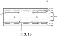
- FIG. 1A is a schematic cross-sectional view for explaining a touch sensitive element according to an exemplary embodiment.
- FIG. 1B is a schematic view for explaining compressive force and tensile force generated in an electroactive layer of a touch sensitive element according to an exemplary embodiment.
- a touch sensitive element 100 includes an electroactive layer 110, an electrode 120, and a hard coating layer 130.
- the electrode 120 applies an electric field to the electroactive layer 110 to induce vibration or bending by an electrical stimulation.
- the electrode 120 may be disposed to have various shapes and various numbers of electrodes may be disposed as needed. For example, as illustrated in FIG. 1A , a plurality of electrodes 120 may be disposed on an upper surface and a lower surface of the electroactive layer 110 or a plurality of electrodes may be disposed on any one of the upper surface and the lower surface of the electroactive layer 110.
- electrodes 120 may be disposed on both the upper surface and the lower surface of the electroactive layer 110.
- the electrode 120 disposed on the upper surface of the electroactive layer 110 extends in an X-axis direction and the electrode 120 disposed on the lower layer of the electroactive layer 110 extends in a Y axis direction to have a vertical arrangement structure in which the electrodes intersect each other to be disposed in a matrix.
- a horizontal arrangement structure in which the electrodes 120 are disposed on only one surface of the electroactive layer 110 may be provided.
- the plurality of electrodes 120 is disposed to be opposite to each other on the upper surface and the lower surface of the electroactive layer 110 in one cell so that a multilayer structure in which both the vertical arrangement structure and the horizontal arrangement structure of the electrode 120 are implemented may be provided.
- the electrode 120 is formed of a conductive material. Further, in order to secure light transmittance of the touch sensitive element 100, the electrode 120 may be formed of a transparent conductive material.
- the electrode 120 may be formed of a transparent conductive material such as indium tin oxide (ITO), indium zinc oxide (IZO), graphene, metal nano wire, and transparent conductive oxide (TCO).
- the electrode 120 may be formed of a metal mesh. That is, the electrode 120 is formed of a metal mesh in which a metal material is disposed to have a mesh type so that the electrode 120 may be configured to be substantially transparently visible.
- a constituent material of the electrode 120 is not limited to the above-described example, but various transparent conductive materials may be used for the constituent material of the electrode 120. When a plurality of electrodes 120 is configured, each of the electrodes may be formed of the same material or different materials.
- the electrode 120 may be formed by various methods.
- the electrode 120 may be formed on the electroactive layer 110 by a method such as sputtering, printing, and slit coating.
- the electroactive layer 110 may refer to a layer which is deformed to generate vibration as a voltage is applied.
- the electroactive layer 110 is formed of an electroactive polymer (EAP) which is deformed by an electrical stimulation.
- EAP electroactive polymer
- the electroactive polymer may be dielectric elastomer or ferroelectric polymer.
- the dielectric elastomer may be one or more kinds selected from the group consisting of acrylic-based polymer, urethane-based polymer, and silicon-based polymer, but is not limited thereto.
- the ferroelectric polymer may be polyvinylidene fluoride-based (hereinafter, PVDF) polymer.
- the PVDF-based polymer refers to a polymer including a PVDF repeating unit in a main chain of the polymer, and for example, may be PVDF homopolymer or PVDF copolymer.
- the electroactive layer 110 is formed of dielectric elastomer
- the dielectric elastomer is contracted or expand by electrostatic attraction (coulombic force) generated as a voltage is applied to the electroactive layer 110 so that the touch sensitive element 100 may be deformed or vibrates.
- electrostatic attraction coulombic force
- the electroactive layer 110 is formed of ferroelectric polymer
- an alignment direction of a dipole in the electroactive layer 110 is changed as the voltage is applied to the electroactive layer 110 so that the touch sensitive element may be deformed. Since the transmittance of a film type electroactive layer 110 is excellent, the touch sensitive element is attached on a front surface of the display panel to be easily applied to the display device.
- an electroactive polymer which forms the electroactive layer 110 has a positive coefficient of thermal expansion (CTE).
- CTE positive coefficient of thermal expansion
- the electroactive polymer having a positive coefficient of thermal expansion expands during a heat treatment process.
- a compressive force is applied to a surface of the electroactive layer 110.
- details of the coefficient of thermal expansion will be described in detail below together with the hard coating layer 130.
- a thickness of the electroactive layer 110 may be determined such that the touch sensitive element 100 generates a sufficient vibration with a low driving voltage.
- the electroactive layer 110 may be 10 ⁇ m to 200 ⁇ m.
- the touch sensitive element 100 may generate sufficient vibration and lower the driving voltage. This is because when the thickness of the electroactive layer 110 is larger than 200 ⁇ m, an excessive driving voltage may be required to drive the touch sensitive element 100.
- the hard coating layer 130 is formed on the electrode 120 and the electroactive layer 110. More specifically, the hard coating layer 130 is disposed so as to be in contact with the electrode 120 and the electroactive layer 110 to be disposed on the electrode 120 and also on the electrode active layer 110 in which the electrode 120 is not disposed.
- the hard coating layer 130 protects an exterior appearance of the touch sensitive element 100 to improve durability and improves hardness of a surface of the electroactive layer 110 to strengthen vibration force which is transmitted from the electroactive layer 110.
- the hard coating layer 130 has a negative coefficient of thermal expansion.
- a heat treatment technique which applies heat is generally used after forming a coating layer by applying a coating composition.
- compressive force is applied to the surface of the electroactive layer 110 disposed below the hard coating layer 130 so that the hardness of the surface of the electroactive layer 110 is increased. Force which is applied to the electroactive layer 110 when the hard coating layer 130 has a negative coefficient of thermal expansion will be specifically described with reference to FIG. 1B .
- FIG. 1B is a schematic view for explaining compressive force and tensile force generated in the electroactive layer 110 of the touch sensitive element 100 according to an exemplary embodiment.
- the electroactive layer 110 may be divided into a center portion 111, an upper surface portion 112 located above the center portion, and a lower surface portion 113 disposed below the center portion 111.
- the upper surface portion 112 and the lower surface portion 113 include arbitrary spaces having a thickness which are disposed on the electroactive layer 110 and the surface and below the surface of the electroactive layer 110 with which the hard coating layer 130 is in contact.
- the center portion 111, the upper surface portion 112, and the lower surface portion 113 are obtained by arbitrarily dividing a space, but are not limited to areas illustrated in FIG. 1B .
- An electroactive polymer which forms the electroactive layer 110 has a positive coefficient of thermal expansion. Therefore, the electroactive layer 110 has a property of horizontally expanding during the heat treatment process on the hard coating layer 130. Accordingly, the electroactive layer 110 which is subjected to the heat treatment process receives the tensile force B in a horizontal direction from the center of the electroactive layer 110 as illustrated in FIG. 1B . Specifically, the center portion 111 of the electroactive layer 110 receives the tensile force B in the horizontal direction.
- the upper surface portion 112 and the lower surface portion 113 of the electroactive layer 110 receive the compressive force A.
- the hard coating layer 130 has a negative thermal expansion coefficient
- the hard coating layer 130 is compressible during the process of performing a heat treatment on the hard coating layer 130. Therefore, the hard coating layer 130 is compressed to the center by the heat treatment process, so that the surface portion of the electroactive layer 110 which is in contact with the hard coating layer 130 also receives a compressible force. That is, the upper surface portion 112 and the lower surface portion 113 of the electroactive layer 110 receive the compressive force A by the hard coating layer 130.
- the hard coating layer 130 is formed so that the center portion 111 of the electroactive layer 110 receives the tensile force B and the upper surface portion 112 and the lower surface portion 113 of the electroactive layer 110 receive the compressive force A.
- the upper surface portion 112 and the lower surface portion 113 of the electroactive layer 110 which receive the compressive force A as compared with the center portion 111, internal storage energy is increased and hardness in a vertical direction of the electroactive layer 110 is also increased. By doing this, vibration force which is transmitted from the center of the electroactive layer 110 to the surface when the electroactive layer 110 vibrates is strengthened. By doing this, even though the same voltage is applied to the electroactive layer 110, the vibration effect may further improved.
- the material for the hard coating layer 130 may be a transparent material having a negative coefficient of thermal expansion. More specifically, the material for the hard coating layer 130 may be a crystalized transparent ceramic material.
- the material for the hard coating layer 130 may be a ceramic material in which silica (SiO 2 ), alumina (Al 2 O 3 ), and lithium oxide (Li 2 O) are crystallized.
- ⁇ -eucryptite ⁇ -Li 2 O ⁇ Al 2 O 3 ⁇ 2SiO 2
- ⁇ -spodumen ⁇ -Li 2 O ⁇ Al 2 O 3 ⁇ 4SiO 2 or ⁇ -Li 2 O ⁇ Al 2 O 3 ⁇ 9SiO 2
- zirconium tungstate ZrW 2 O 8
- hafnium tungstate HfW 2 O 8
- zirconium molybdate ZrMO 2 O 8
- hafnium molybdate HfMO 2 O 8
- the hard coating layer 130 may be formed by applying a composition including a ceramic material having a negative coefficient of thermal expansion on the electroactive layer 110 and then sintering the composition through a heat treatment process. In the meantime, the heat treatment process may be subjected to a plurality of cycles of repeatedly treating the low temperature and the high temperature. A stronger compressive force may be applied to the electroactive layer 110 through a plurality of cycles depending on the material which configures the hard coating layer 130.
- the hard coating layer 130 is formed above the electrode 120 and the electroactive layer 110. This is because when the hard coating layer 130 is disposed below the electrode 120, that is, disposed between the electrode 120 and the electroactive layer 110, a vibration level of the touch sensitive element 100 is lowered. Generally, since the hard coating layer 130 having a negative coefficient of thermal expansion has a very small permittivity, when the hard coating layer 130 is disposed between the electrode 120 and the electroactive layer 110, the hard coating layer 130 may act to interfere with the vibration of the electroactive layer 110.
- the hard coating layer 130 may be disposed to cover the surfaces of the electrode 120 and the electroactive layer 110.
- the hard coating layer 130 needs to be disposed to be in contact with the surface of the electroactive layer 110 to apply sufficient compressive force to the surface portion of the electroactive layer 110 when the hard coating layer 130 is formed and also serve as a protective layer of the touch sensitive element 100.
- a thickness of the hard coating layer 130 may be 10 nm to 200 nm.
- the thickness of the hard coating layer 130 means a thickness from the surface of the electroactive layer 110 on which the hard coating layer 130 is disposed.
- sufficient tensile force may be applied to the surface portion of the electroactive layer 110 and the hard coating layer may serve as a protective layer having a sufficient hardness within a range that does not interfere with the movement of the entire contact sensitive element 100.
- An electroactive layer was formed to have a thickness of 20 ⁇ m using acrylic-based polymer, and then an upper electrode and a lower electrode were deposited on both surfaces. Thereafter, silica (SiO 2 ) sol, Al(NO 3 ) 3 ⁇ 9H 2 O, and LiNO 3 were mixed and stirred in distilled water for 3 hours, and a PVA solution was added and stirred for 3 hours to prepare a coating composition in a gel state. The prepared coating composition was coated to cover both the electroactive layer and the electrode and then heat-treated at 150°C for 24 hours to form a hard coating layer with a thickness of 50 nm formed of LiO 2 ⁇ Al 2 O 3 ⁇ 4SiO 2 spodumene. In this case, the coefficient of thermal expansion of the hard coating layer was -0.14 x 10 -6 /°C.
- the touch sensitive element was prepared by the same method as the first exemplary embodiment except that the hard coating layer was not formed.
- FIG. 2 is a schematic cross-sectional view for explaining a touch sensitive element 200 according to a comparative embodiment.
- a hard coating layer 230 was disposed between an electroactive layer 110 and an electrode 220.
- the touch sensitive element 200 of FIG. 2 was prepared by the same method as the first exemplary embodiment except that an electrode 220 was deposited after forming the hard coating layer 230 directly on the electroactive layer 110.
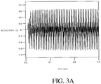
- a vibration acceleration when a voltage of 400 V was applied to an upper electrode under a condition of 100 Hz and a ground voltage was applied to a lower electrode was measured. Measurement results were illustrated in FIGS. 3A , 3B , and 3C .
- FIGS. 3A , 3B , and 3C are graphs obtained by measuring a vibration acceleration of a touch sensitive element of a first exemplary embodiment, a first comparative embodiment, and a second comparative embodiment.
- the first exemplary embodiment represented a vibration acceleration of approximately 0.9 G
- the first comparative embodiment represented a vibration acceleration of approximately 0.6 G. That is, it was confirmed that the touch sensitive element according to the first exemplary embodiment in which the hard coating layer having a negative coefficient of thermal expansion was formed had significantly higher vibration acceleration at the same voltage as compared with the first comparative embodiment in which the hard coating layer was not formed.
- a vibration level of the touch sensitive element according to the first exemplary embodiment needed to be high. It was also confirmed that in order to obtain the same vibration level, a lower voltage was required for the first exemplary embodiment as compared with the first comparative embodiment.
- the vibration acceleration was significantly high as compared with a case when the hard coating layer was disposed between the electroactive layer and the electrode. It was confirmed that when the hard coating layer was disposed between the electroactive layer and the electrode, the vibration acceleration was reduced as compared with the first comparative embodiment in which the hard coating layer was not disposed.
- the hard coating layer having a low permittivity is disposed between the electrodes and the electroactive layer, so that the vibration level of the touch sensitive element is lowered.
- the touch sensitive element As described above, a hard coating layer having a negative coefficient of thermal expansion is disposed above the electroactive layer which is formed of an electroactive polymer having a positive coefficient of thermal expansion and the electrode so that the vibration level of the touch sensitive element is significantly improved and a protective layer having an excellent hardness is provided on an exterior appearance of the touch sensitive element. Therefore, the touch sensitive element according to an exemplary embodiment has an improved impact resistance and also transmits direct vibration feeling to the user.
- FIG. 4 is a schematic cross-sectional view for explaining a display device including a touch sensitive element according to an exemplary embodiment.
- a display device 400 includes a display panel 440, a contact sensitive device 100, a touch panel 450, and a cover 460.
- the touch sensitive element 100 included in the display device 400 of FIG. 4 is the same as the touch sensitive element 100 according to the exemplary embodiment which has been described with reference to FIG. 1A . Therefore, a redundant description of the touch sensitive element 100 will be omitted.
- the display panel 440 refers to a panel in which a display element for displaying an image in the display device 400 is disposed.
- various display panels such as an organic light emitting display panel, a liquid crystal display panel, and an electrophoretic display panel may be used.
- the touch sensitive element 100 including an electroactive layer 110, an electrode 120, and a hard coating layer 130 is disposed.
- the touch sensitive element illustrated in FIG. 4 is the touch sensitive element 100 illustrated in FIG. 1A .
- the touch sensitive element 100 includes an electroactive layer 110 which is formed of an electroactive polymer, an electrode 120 which is disposed on at least one surface of the electroactive layer 110, and a hard coating layer 130 which is disposed on the electroactive layer and the electrode 120 and has a negative coefficient of thermal expansion.
- a touch panel 450 is disposed on the touch sensitive element 100.
- the touch panel 450 refers to a panel which senses a user's touch input to the display device 400.
- As the touch panel 450 for example, a capacitive type, a resistive overlay type, an ultrasonic type, or an infrared type may be used, but a capacitive type touch panel may be used as the touch panel 450.
- the display device 400 illustrated in FIG. 4 includes an add-on type touch panel 450 in which a separately manufactured touch panel 450 is separately disposed on the display panel 440.
- a cover 460 is disposed on the touch panel 450.
- the cover 460 is a configuration for protecting the display device from an impact from the outside of the display device 400.
- the cover 460 may be formed of a transparent insulating material.
- an adhesive layer may be used to bond the display panel 440, the touch sensitive element 100, the touch panel 450, and the cover 460 to each other.
- an adhesive layer for example, an optical clear adhesive (OCA) or an optical clear resin (OCR) may be used, but the adhesive layer is not limited thereto.
- the touch sensitive element including the electroactive layer formed of an electroactive polymer has an excellent transparency, but has a lower vibration level than that of the touch sensitive element of the related art. Therefore, a driving voltage which is too high to introduce a touch sensitive element in a small display device such as a mobile device is required.
- the display device according to the exemplary embodiment uses a touch sensitive element which is transparent and has an improved vibration level so that the driving voltage may be lowered.
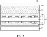
- FIG. 5 is a schematic cross-sectional view for explaining a display device including a touch sensitive element according to another exemplary embodiment.
- a display device 500 illustrated in FIG. 5 is compared with the display device 400 which has been described with reference to FIG. 4 , except that the display panel 540 is a liquid crystal display panel and thus a backlight unit is further included and an in-cell type touch sensor in which a touch sensor other than the separate touch panel is provided to be integrated with the display panel 540 is configured, other components are substantially the same, so that the redundant description will be omitted.
- the display panel 540 is disposed between the cover 460 and the touch sensitive element 100.
- the liquid crystal display panel displays an image by adjusting transmittance of the light emitted from the backlight unit 570.
- the liquid display panel includes a lower polarizer, a lower substrate including a thin film transistor (TFT), a liquid crystal layer, an upper substrate including a color filter, and an upper polarizer, but is not limited thereto.
- TFT thin film transistor
- the display panel 540 is a panel in which a display device for displaying an image in the display device 500 is disposed and includes a touch sensor configured to be integrated in the panel. That is, the touch sensor is disposed in the display panel 540 to configure an in-cell touch sensor. In the in-cell type touch sensor, a common electrode of the display panel 540 is simultaneously used as a touch electrode.
- the display device 500 illustrated in FIG. 5 is a liquid crystal display device so that a backlight unit 570 which emits light toward the display panel 540 is disposed below the display panel 540.
- the touch sensitive element 100 including an electroactive layer 110, an electrode 120, and a hard coating layer 130 is disposed.
- the touch sensitive element when the display panel is a liquid crystal display panel and an in-cell type touch sensor is integrated with the display panel, if the touch sensitive element is disposed on the touch sensor, the touch input may be erroneously recognized due to a noise which may be generated by a high driving voltage applied to the touch sensitive element. Therefore, the touch sensitive element may be disposed below the display panel. However, when the touch sensitive element is disposed below the display panel, since the user is located far away from the position to which the touch input is applied, the vibration level transmitted to the user is reduced. Therefore, in order to minimize the reduction of the vibration level, it is considered to dispose the touch sensitive element between the liquid crystal display panel and the backlight unit.
- the shape memory alloy or the piezoelectric ceramics used in the touch sensitive element of the related art has low light transmittance.
- a hard coating layer having a negative coefficient of thermal expansion is disposed on the electroactive layer formed of an electroactive polymer and the electrode so that the transparency is excellent and the vibration level is improved. Therefore, even though the touch sensitive element 100 is disposed between the liquid crystal display panel and the backlight unit, the light transmittance of the light supplied from the backlight unit to the liquid crystal display panel is excellent and stronger vibration may be transmitted than in the case of using the electroactive polymer in the related art.
- a touch sensitive element including an electroactive layer which is formed of electroactive polymer (EAP), an electrode which is disposed on at least one surface of the electroactive layer, and a hard coating layer which is disposed on the electroactive layer and the electrode and has a negative coefficient of thermal expansion (CTE).
- EAP electroactive polymer
- CTE negative coefficient of thermal expansion
- the electroactive layer may have a positive coefficient of thermal expansion.
- the hard coating layer may include eucryptite or spodumene which is formed of silica (SiO 2 ), alumina (Al 2 O 3 ), and lithium oxide (Li 2 O).
- the hard coating layer may include at least one of zirconium tungstate (ZrW 2 O 8 ), hafnium tungstate (HfW 2 O 8 ), zirconium molybdate (ZrMO 2 O 8 ), and hafnium molybdate (HfMO 2 O 8 ).
- the hard coating layer may be formed by a heat treatment process of repeatedly treating the low temperature and the high temperature.
- the electroactive layer may be formed of a center portion, an upper surface portion above the center portion, and a lower surface portion below the center portion, and when a voltage is not applied to the electrode, the center portion receives tensile force and the upper surface portion and the lower surface portion receive compressive force.
- a thickness of the hard coating layer may be 10 nm to 200 nm.
- the hard coating layer may cover surfaces of the electrode and the electroactive layer.
- a display device including a display panel and a touch sensitive element above or below the display panel, in which the touch sensitive element includes an electroactive layer formed of an electroactive polymer, an electrode which is disposed on at least one surface of the electroactive layer, and a hard coating layer which is disposed on the electroactive layer and the electrode and has a negative coefficient of thermal expansion.
- the electroactive layer may have a positive coefficient of thermal expansion.
- the display device may further include an add-on type touch panel which is separately disposed on the display panel and the touch sensitive element may be disposed between the display panel and the touch panel.
- the display panel may be a liquid crystal display panel including a touch sensor which is configured to be integrated in the display panel, a backlight unit disposed below the liquid crystal display panel may be further included, and the touch sensitive element may be disposed between the liquid crystal display panel and the backlight unit.
Landscapes
- Engineering & Computer Science (AREA)
- General Engineering & Computer Science (AREA)
- Theoretical Computer Science (AREA)
- Physics & Mathematics (AREA)
- General Physics & Mathematics (AREA)
- Human Computer Interaction (AREA)
- Nonlinear Science (AREA)
- Chemical & Material Sciences (AREA)
- Crystallography & Structural Chemistry (AREA)
- Mathematical Physics (AREA)
- Optics & Photonics (AREA)
- Manufacturing & Machinery (AREA)
- Ceramic Engineering (AREA)
- Position Input By Displaying (AREA)
- User Interface Of Digital Computer (AREA)
- Laminated Bodies (AREA)
Abstract
Description
- The present disclosure relates to a touch sensitive element, a display device including the same, and a manufacturing method thereof, and more particularly, to a touch sensitive element with an improved vibration level and a display device including the same.
- Recently, in response to a demand of users who want to use various display devices including a liquid crystal display device and an organic light emitting display device, a touch type display device which touches a display device to input information is broadly used. Therefore, researches continue to utilize a haptic device to provide direct and various touch feedback to the users. Specifically, a haptic device of the related art is attached on a rear surface of a display panel, so that it is difficult to provide immediate and delicate feedback for the user's touch. Therefore, research is actively performed to provide feedback which is sensitive to the user's touch by positioning the haptic device above the display panel.
- According to the related art, a vibration motor such as an eccentric rotating mass (ERM) or a linear resonant actuator (LRA) is used for the display device as a haptic device. The vibration motor is configured to vibrate the entire display device. Therefore, there are problems in that a size of a mass needs to be increased in order to increase a vibration level, it is difficult to modulate a frequency to adjust the vibration level, and a response speed is very slow. Further, the eccentric rotating mass and the resonant actuator are formed of an opaque material so that it is difficult to dispose the eccentric rotating mass and the resonant actuator above the display panel.
- In order to solve the above-described problems, a shape memory alloy (SMA) and electro-active ceramics (EAC) have been developed as a material for the haptic device. However, the shape memory alloy (SMA) has a slow response speed and a short life-span and is formed of an opaque material. Further, the electro-active ceramics has a low durability against the external impact so that the electro-active ceramics are easily broken due to an external impact and are opaque. Further, it is difficult to make the electro-active ceramics thinner.
- Therefore, the present disclosure has been made in an effort to provide a touch sensitive element which may implement an excellent haptic effect at a low driving voltage by maximizing a vibration effect of an electroactive layer and a display device including the same.
- Further, the present disclosure has been made in an effort to provide a touch sensitive element which is transparent and has excellent surface hardness and a display device including the same.
- The present disclosure is not limited to the above-mentioned aims, and other aims and advantages, which are not mentioned above, can be clearly understood by those skilled in the art from the following description and drawings.
- Aspects of an invention are defined in the appended independent claims.
- There is provided a touch sensitive element including an electroactive layer which is formed of electroactive polymer (EAP), an electrode which is disposed on at least one surface of the electroactive layer, and a hard coating layer which is disposed on the electroactive layer and the electrode and has a negative coefficient of thermal expansion (CTE), thereby maximizing vibration effect in a vertical direction and improving impact resistance.
- There is further provided a display device including: a display panel and a touch sensitive element above or below the display panel, in which the touch sensitive element includes an electroactive layer formed of an electroactive polymer, an electrode which is disposed on at least one surface of the electroactive layer, and a hard coating layer which is disposed on the electroactive layer and the electrode and has a negative coefficient of thermal expansion.
- Other detailed matters of the exemplary embodiments are included in the detailed description and the drawings.
- A vibration effect in a vertical direction may be maximized by changing a characteristic of a surface of an electroactive layer and thus an excellent haptic effect may be implemented at a low driving voltage.
- Further, the touch sensitive element is transparent and a hardness of the surface is excellent so that impact resistance is improved.
- The effects are not limited to the contents exemplified above, and more various effects are included in the present specification.
-
-
FIG. 1A is a schematic cross-sectional view for explaining a touch sensitive element according to an exemplary embodiment; -
FIG. 1B is a schematic view for explaining compressive force and tensile force generated in an electroactive layer of a touch sensitive element according to an exemplary embodiment; -
FIG. 2 is a schematic cross-sectional view for explaining a touch sensitive element according to a comparative embodiment; -
FIGS. 3A ,3B , and3C are graphs obtained by measuring a vibration acceleration of a touch sensitive element of a first exemplary embodiment, a first comparative embodiment, and a second comparative embodiment; -
FIG. 4 is a schematic cross-sectional view for explaining a display device including a touch sensitive element according to an exemplary embodiment; and -
FIG. 5 is a schematic cross-sectional view for explaining a display device including a touch sensitive element according to another exemplary embodiment. - Advantages and characteristics of the present disclosure and a method of achieving the advantages and characteristics will be clear by referring to exemplary embodiments described below in detail together with the accompanying drawings. However, the present disclosure is not limited to exemplary embodiments disclosed herein but may be implemented in various forms. The exemplary embodiments are provided by way of example only so that a person of ordinary skilled in the art can fully understand the present disclosure. Therefore, the present disclosure will be defined by the scope of the appended claims.
- The shapes, sizes, ratios, angles, numbers, and the like illustrated in the accompanying drawings for describing the exemplary embodiments are merely examples, and the present disclosure is not limited thereto. Further, in the following description of the present disclosure, a detailed explanation of known related technologies may be omitted to avoid unnecessarily obscuring the subject matter of the present disclosure. The terms such as "including," "having," and "comprising" used herein are generally intended to allow other components to be added unless the terms are used with the term "only". Any references to singular may include plural unless expressly stated otherwise.
- Components are interpreted to include an ordinary error range even if not expressly stated.
- When the position relation between two parts is described using the terms such as "on", "above", "below", and "next", one or more parts may be positioned between the two parts unless the terms are used with the term "immediately" or "directly" is not used.
- When an element or layer is disposed "on" other element or layer, another layer or another element may be interposed directly on the other element or therebetween.
- Although the terms "first", "second", and the like are used for describing various components, these components are not confined by these terms. These terms are merely used for distinguishing one component from the other components. Therefore, a first component to be mentioned below may be a second component in a technical concept of the present disclosure.
- Like reference numerals generally denote like elements throughout the specification.
- A size and a thickness of each component illustrated in the drawing are illustrated for convenience of description, and the present disclosure is not limited to the size and the thickness of the component illustrated.
- The features of various embodiments be partially or entirely coupled to or combined with each other and can be interlocked and operated in technically various ways, and the embodiments can be carried out independently of or in association with each other.
- Hereinafter, various exemplary embodiments will be described in detail with reference to accompanying drawings.
-
FIG. 1A is a schematic cross-sectional view for explaining a touch sensitive element according to an exemplary embodiment.FIG. 1B is a schematic view for explaining compressive force and tensile force generated in an electroactive layer of a touch sensitive element according to an exemplary embodiment. Referring toFIGS. 1A and1B , a touchsensitive element 100 includes anelectroactive layer 110, anelectrode 120, and ahard coating layer 130. - The
electrode 120 applies an electric field to theelectroactive layer 110 to induce vibration or bending by an electrical stimulation. Theelectrode 120 may be disposed to have various shapes and various numbers of electrodes may be disposed as needed. For example, as illustrated inFIG. 1A , a plurality ofelectrodes 120 may be disposed on an upper surface and a lower surface of theelectroactive layer 110 or a plurality of electrodes may be disposed on any one of the upper surface and the lower surface of theelectroactive layer 110. - Specifically,
electrodes 120 may be disposed on both the upper surface and the lower surface of theelectroactive layer 110. In this case, theelectrode 120 disposed on the upper surface of theelectroactive layer 110 extends in an X-axis direction and theelectrode 120 disposed on the lower layer of theelectroactive layer 110 extends in a Y axis direction to have a vertical arrangement structure in which the electrodes intersect each other to be disposed in a matrix. Further, a horizontal arrangement structure in which theelectrodes 120 are disposed on only one surface of theelectroactive layer 110 may be provided. Further, the plurality ofelectrodes 120 is disposed to be opposite to each other on the upper surface and the lower surface of theelectroactive layer 110 in one cell so that a multilayer structure in which both the vertical arrangement structure and the horizontal arrangement structure of theelectrode 120 are implemented may be provided. - The
electrode 120 is formed of a conductive material. Further, in order to secure light transmittance of the touchsensitive element 100, theelectrode 120 may be formed of a transparent conductive material. For example, theelectrode 120 may be formed of a transparent conductive material such as indium tin oxide (ITO), indium zinc oxide (IZO), graphene, metal nano wire, and transparent conductive oxide (TCO). Further, theelectrode 120 may be formed of a metal mesh. That is, theelectrode 120 is formed of a metal mesh in which a metal material is disposed to have a mesh type so that theelectrode 120 may be configured to be substantially transparently visible. A constituent material of theelectrode 120 is not limited to the above-described example, but various transparent conductive materials may be used for the constituent material of theelectrode 120. When a plurality ofelectrodes 120 is configured, each of the electrodes may be formed of the same material or different materials. - The
electrode 120 may be formed by various methods. For example, theelectrode 120 may be formed on theelectroactive layer 110 by a method such as sputtering, printing, and slit coating. - The
electroactive layer 110 may refer to a layer which is deformed to generate vibration as a voltage is applied. Theelectroactive layer 110 is formed of an electroactive polymer (EAP) which is deformed by an electrical stimulation. For example, the electroactive polymer may be dielectric elastomer or ferroelectric polymer. Specifically, the dielectric elastomer may be one or more kinds selected from the group consisting of acrylic-based polymer, urethane-based polymer, and silicon-based polymer, but is not limited thereto. Further, the ferroelectric polymer may be polyvinylidene fluoride-based (hereinafter, PVDF) polymer. The PVDF-based polymer refers to a polymer including a PVDF repeating unit in a main chain of the polymer, and for example, may be PVDF homopolymer or PVDF copolymer. - When the
electroactive layer 110 is formed of dielectric elastomer, the dielectric elastomer is contracted or expand by electrostatic attraction (coulombic force) generated as a voltage is applied to theelectroactive layer 110 so that the touchsensitive element 100 may be deformed or vibrates. When theelectroactive layer 110 is formed of ferroelectric polymer, an alignment direction of a dipole in theelectroactive layer 110 is changed as the voltage is applied to theelectroactive layer 110 so that the touch sensitive element may be deformed. Since the transmittance of a film typeelectroactive layer 110 is excellent, the touch sensitive element is attached on a front surface of the display panel to be easily applied to the display device. - In this case, an electroactive polymer which forms the
electroactive layer 110 has a positive coefficient of thermal expansion (CTE). The electroactive polymer having a positive coefficient of thermal expansion expands during a heat treatment process. During a process of forming ahard coating layer 130 having a negative coefficient of thermal expansion, a compressive force is applied to a surface of theelectroactive layer 110. With regard to this, details of the coefficient of thermal expansion will be described in detail below together with thehard coating layer 130. - In the meantime, a thickness of the
electroactive layer 110 may be determined such that the touchsensitive element 100 generates a sufficient vibration with a low driving voltage. For example, theelectroactive layer 110 may be 10 µm to 200 µm. When a thickness of theelectroactive layer 110 satisfies the above-mentioned range, the touchsensitive element 100 may generate sufficient vibration and lower the driving voltage. This is because when the thickness of theelectroactive layer 110 is larger than 200 µm, an excessive driving voltage may be required to drive the touchsensitive element 100. - The
hard coating layer 130 is formed on theelectrode 120 and theelectroactive layer 110. More specifically, thehard coating layer 130 is disposed so as to be in contact with theelectrode 120 and theelectroactive layer 110 to be disposed on theelectrode 120 and also on the electrodeactive layer 110 in which theelectrode 120 is not disposed. Thehard coating layer 130 protects an exterior appearance of the touchsensitive element 100 to improve durability and improves hardness of a surface of theelectroactive layer 110 to strengthen vibration force which is transmitted from theelectroactive layer 110. - The
hard coating layer 130 has a negative coefficient of thermal expansion. When thehard coating layer 130 is disposed on theelectroactive layer 110, a heat treatment technique which applies heat is generally used after forming a coating layer by applying a coating composition. In this case, when thehard coating layer 130 has a negative coefficient of thermal expansion, compressive force is applied to the surface of theelectroactive layer 110 disposed below thehard coating layer 130 so that the hardness of the surface of theelectroactive layer 110 is increased. Force which is applied to theelectroactive layer 110 when thehard coating layer 130 has a negative coefficient of thermal expansion will be specifically described with reference toFIG. 1B . -
FIG. 1B is a schematic view for explaining compressive force and tensile force generated in theelectroactive layer 110 of the touchsensitive element 100 according to an exemplary embodiment. Referring toFIG. 1B , theelectroactive layer 110 may be divided into acenter portion 111, anupper surface portion 112 located above the center portion, and alower surface portion 113 disposed below thecenter portion 111. Theupper surface portion 112 and thelower surface portion 113 include arbitrary spaces having a thickness which are disposed on theelectroactive layer 110 and the surface and below the surface of theelectroactive layer 110 with which thehard coating layer 130 is in contact. In this case, thecenter portion 111, theupper surface portion 112, and thelower surface portion 113 are obtained by arbitrarily dividing a space, but are not limited to areas illustrated inFIG. 1B . - An electroactive polymer which forms the
electroactive layer 110 has a positive coefficient of thermal expansion. Therefore, theelectroactive layer 110 has a property of horizontally expanding during the heat treatment process on thehard coating layer 130. Accordingly, theelectroactive layer 110 which is subjected to the heat treatment process receives the tensile force B in a horizontal direction from the center of theelectroactive layer 110 as illustrated inFIG. 1B . Specifically, thecenter portion 111 of theelectroactive layer 110 receives the tensile force B in the horizontal direction. - Differently from this, the
upper surface portion 112 and thelower surface portion 113 of theelectroactive layer 110 receive the compressive force A. Specifically, since thehard coating layer 130 has a negative thermal expansion coefficient, thehard coating layer 130 is compressible during the process of performing a heat treatment on thehard coating layer 130. Therefore, thehard coating layer 130 is compressed to the center by the heat treatment process, so that the surface portion of theelectroactive layer 110 which is in contact with thehard coating layer 130 also receives a compressible force. That is, theupper surface portion 112 and thelower surface portion 113 of theelectroactive layer 110 receive the compressive force A by thehard coating layer 130. - As a result, the
hard coating layer 130 is formed so that thecenter portion 111 of theelectroactive layer 110 receives the tensile force B and theupper surface portion 112 and thelower surface portion 113 of theelectroactive layer 110 receive the compressive force A. In theupper surface portion 112 and thelower surface portion 113 of theelectroactive layer 110 which receive the compressive force A, as compared with thecenter portion 111, internal storage energy is increased and hardness in a vertical direction of theelectroactive layer 110 is also increased. By doing this, vibration force which is transmitted from the center of theelectroactive layer 110 to the surface when theelectroactive layer 110 vibrates is strengthened. By doing this, even though the same voltage is applied to theelectroactive layer 110, the vibration effect may further improved. - As a material for the
hard coating layer 130, a transparent material having a negative coefficient of thermal expansion may be used. More specifically, the material for thehard coating layer 130 may be a crystalized transparent ceramic material. For example, the material for thehard coating layer 130 may be a ceramic material in which silica (SiO2), alumina (Al2O3), and lithium oxide (Li2O) are crystallized. For example, β-eucryptite (β-Li2O·Al2O3·2SiO2) or β-spodumen (β-Li2O·Al2O3·4SiO2 or β-Li2O·Al2O3·9SiO2) may be used or zirconium tungstate (ZrW2O8) or hafnium tungstate (HfW2O8), zirconium molybdate (ZrMO2O8) or hafnium molybdate (HfMO2O8) may be used, but the material is not limited thereto. - The
hard coating layer 130 may be formed by applying a composition including a ceramic material having a negative coefficient of thermal expansion on theelectroactive layer 110 and then sintering the composition through a heat treatment process. In the meantime, the heat treatment process may be subjected to a plurality of cycles of repeatedly treating the low temperature and the high temperature. A stronger compressive force may be applied to theelectroactive layer 110 through a plurality of cycles depending on the material which configures thehard coating layer 130. - The
hard coating layer 130 is formed above theelectrode 120 and theelectroactive layer 110. This is because when thehard coating layer 130 is disposed below theelectrode 120, that is, disposed between theelectrode 120 and theelectroactive layer 110, a vibration level of the touchsensitive element 100 is lowered. Generally, since thehard coating layer 130 having a negative coefficient of thermal expansion has a very small permittivity, when thehard coating layer 130 is disposed between theelectrode 120 and theelectroactive layer 110, thehard coating layer 130 may act to interfere with the vibration of theelectroactive layer 110. - Specifically, the
hard coating layer 130 may be disposed to cover the surfaces of theelectrode 120 and theelectroactive layer 110. Thehard coating layer 130 needs to be disposed to be in contact with the surface of theelectroactive layer 110 to apply sufficient compressive force to the surface portion of theelectroactive layer 110 when thehard coating layer 130 is formed and also serve as a protective layer of the touchsensitive element 100. - A thickness of the
hard coating layer 130 may be 10 nm to 200 nm. In this case, the thickness of thehard coating layer 130 means a thickness from the surface of theelectroactive layer 110 on which thehard coating layer 130 is disposed. When the thickness of thehard coating layer 130 satisfies the above-mentioned range, sufficient tensile force may be applied to the surface portion of theelectroactive layer 110 and the hard coating layer may serve as a protective layer having a sufficient hardness within a range that does not interfere with the movement of the entire contactsensitive element 100. - Hereinafter, the present disclosure will be described in detail through the exemplary embodiments. However, the following exemplary embodiments are set forth to illustrate the present disclosure, but the scope of the appended claims is not limited thereto.
- An electroactive layer was formed to have a thickness of 20 µm using acrylic-based polymer, and then an upper electrode and a lower electrode were deposited on both surfaces. Thereafter, silica (SiO2) sol, Al(NO3)3·9H2O, and LiNO3 were mixed and stirred in distilled water for 3 hours, and a PVA solution was added and stirred for 3 hours to prepare a coating composition in a gel state. The prepared coating composition was coated to cover both the electroactive layer and the electrode and then heat-treated at 150°C for 24 hours to form a hard coating layer with a thickness of 50 nm formed of LiO2·Al2O3·4SiO2 spodumene. In this case, the coefficient of thermal expansion of the hard coating layer was -0.14 x 10⁻⁶/°C.
- The touch sensitive element was prepared by the same method as the first exemplary embodiment except that the hard coating layer was not formed.
-
FIG. 2 is a schematic cross-sectional view for explaining a touchsensitive element 200 according to a comparative embodiment. Referring toFIG. 2 , ahard coating layer 230 was disposed between anelectroactive layer 110 and anelectrode 220. The touchsensitive element 200 ofFIG. 2 was prepared by the same method as the first exemplary embodiment except that anelectrode 220 was deposited after forming thehard coating layer 230 directly on theelectroactive layer 110. - In the touch sensitive element according to the first exemplary embodiment, the first comparative embodiment, and the second comparative embodiment, a vibration acceleration when a voltage of 400 V was applied to an upper electrode under a condition of 100 Hz and a ground voltage was applied to a lower electrode was measured. Measurement results were illustrated in
FIGS. 3A ,3B , and3C . -
FIGS. 3A ,3B , and3C are graphs obtained by measuring a vibration acceleration of a touch sensitive element of a first exemplary embodiment, a first comparative embodiment, and a second comparative embodiment. WhenFIGS. 3A and3B are compared, it was confirmed that the first exemplary embodiment represented a vibration acceleration of approximately 0.9 G and the first comparative embodiment represented a vibration acceleration of approximately 0.6 G. That is, it was confirmed that the touch sensitive element according to the first exemplary embodiment in which the hard coating layer having a negative coefficient of thermal expansion was formed had significantly higher vibration acceleration at the same voltage as compared with the first comparative embodiment in which the hard coating layer was not formed. In other words, it was confirmed that at the same applied voltage, a vibration level of the touch sensitive element according to the first exemplary embodiment needed to be high. It was also confirmed that in order to obtain the same vibration level, a lower voltage was required for the first exemplary embodiment as compared with the first comparative embodiment. - Further, when
FIGS. 3A and3C were compared, it was confirmed that in the second comparative embodiment, the vibration acceleration was approximately 0.5 G. - From the first exemplary embodiment and the second comparative embodiment, it was confirmed that when the hard coating layer having a negative coefficient of thermal expansion was disposed above the electroactive layer and the electrode, the vibration acceleration was significantly high as compared with a case when the hard coating layer was disposed between the electroactive layer and the electrode. It was confirmed that when the hard coating layer was disposed between the electroactive layer and the electrode, the vibration acceleration was reduced as compared with the first comparative embodiment in which the hard coating layer was not disposed. This is because even though the compressive force is generated on the surface portion of the electroactive layer so that the vibration force which is transmitted to a vertical direction of the electroactive layer is increased, the hard coating layer having a low permittivity is disposed between the electrodes and the electroactive layer, so that the vibration level of the touch sensitive element is lowered.
- As described above, a hard coating layer having a negative coefficient of thermal expansion is disposed above the electroactive layer which is formed of an electroactive polymer having a positive coefficient of thermal expansion and the electrode so that the vibration level of the touch sensitive element is significantly improved and a protective layer having an excellent hardness is provided on an exterior appearance of the touch sensitive element. Therefore, the touch sensitive element according to an exemplary embodiment has an improved impact resistance and also transmits direct vibration feeling to the user.
-
FIG. 4 is a schematic cross-sectional view for explaining a display device including a touch sensitive element according to an exemplary embodiment. Referring toFIG. 4 , adisplay device 400 includes adisplay panel 440, a contactsensitive device 100, atouch panel 450, and acover 460. In this case, the touchsensitive element 100 included in thedisplay device 400 ofFIG. 4 is the same as the touchsensitive element 100 according to the exemplary embodiment which has been described with reference toFIG. 1A . Therefore, a redundant description of the touchsensitive element 100 will be omitted. - The
display panel 440 refers to a panel in which a display element for displaying an image in thedisplay device 400 is disposed. As thedisplay panel 440, for example, various display panels such as an organic light emitting display panel, a liquid crystal display panel, and an electrophoretic display panel may be used. - On the
display panel 440, the touchsensitive element 100 including anelectroactive layer 110, anelectrode 120, and ahard coating layer 130 is disposed. Hereinafter, it will be described that the touch sensitive element illustrated inFIG. 4 is the touchsensitive element 100 illustrated inFIG. 1A . Specifically, the touchsensitive element 100 includes anelectroactive layer 110 which is formed of an electroactive polymer, anelectrode 120 which is disposed on at least one surface of theelectroactive layer 110, and ahard coating layer 130 which is disposed on the electroactive layer and theelectrode 120 and has a negative coefficient of thermal expansion. - A
touch panel 450 is disposed on the touchsensitive element 100. Thetouch panel 450 refers to a panel which senses a user's touch input to thedisplay device 400. As thetouch panel 450, for example, a capacitive type, a resistive overlay type, an ultrasonic type, or an infrared type may be used, but a capacitive type touch panel may be used as thetouch panel 450. Thedisplay device 400 illustrated inFIG. 4 includes an add-ontype touch panel 450 in which a separately manufacturedtouch panel 450 is separately disposed on thedisplay panel 440. - A
cover 460 is disposed on thetouch panel 450. Thecover 460 is a configuration for protecting the display device from an impact from the outside of thedisplay device 400. Thecover 460 may be formed of a transparent insulating material. - Even though not illustrated in
FIG. 4 , an adhesive layer may be used to bond thedisplay panel 440, the touchsensitive element 100, thetouch panel 450, and thecover 460 to each other. As the adhesive layer, for example, an optical clear adhesive (OCA) or an optical clear resin (OCR) may be used, but the adhesive layer is not limited thereto. - Generally, the touch sensitive element including the electroactive layer formed of an electroactive polymer has an excellent transparency, but has a lower vibration level than that of the touch sensitive element of the related art. Therefore, a driving voltage which is too high to introduce a touch sensitive element in a small display device such as a mobile device is required. However, the display device according to the exemplary embodiment uses a touch sensitive element which is transparent and has an improved vibration level so that the driving voltage may be lowered.
-
FIG. 5 is a schematic cross-sectional view for explaining a display device including a touch sensitive element according to another exemplary embodiment. When adisplay device 500 illustrated inFIG. 5 is compared with thedisplay device 400 which has been described with reference toFIG. 4 , except that thedisplay panel 540 is a liquid crystal display panel and thus a backlight unit is further included and an in-cell type touch sensor in which a touch sensor other than the separate touch panel is provided to be integrated with thedisplay panel 540 is configured, other components are substantially the same, so that the redundant description will be omitted. - Referring to
FIG. 5 , thedisplay panel 540 is disposed between thecover 460 and the touchsensitive element 100. The liquid crystal display panel displays an image by adjusting transmittance of the light emitted from thebacklight unit 570. The liquid display panel includes a lower polarizer, a lower substrate including a thin film transistor (TFT), a liquid crystal layer, an upper substrate including a color filter, and an upper polarizer, but is not limited thereto. - The
display panel 540 is a panel in which a display device for displaying an image in thedisplay device 500 is disposed and includes a touch sensor configured to be integrated in the panel. That is, the touch sensor is disposed in thedisplay panel 540 to configure an in-cell touch sensor. In the in-cell type touch sensor, a common electrode of thedisplay panel 540 is simultaneously used as a touch electrode. - Since the
display device 500 illustrated inFIG. 5 is a liquid crystal display device so that abacklight unit 570 which emits light toward thedisplay panel 540 is disposed below thedisplay panel 540. - Between the
display panel 540 and the backlight unit 570, the touchsensitive element 100 including anelectroactive layer 110, anelectrode 120, and ahard coating layer 130 is disposed. - Generally, when the display panel is a liquid crystal display panel and an in-cell type touch sensor is integrated with the display panel, if the touch sensitive element is disposed on the touch sensor, the touch input may be erroneously recognized due to a noise which may be generated by a high driving voltage applied to the touch sensitive element. Therefore, the touch sensitive element may be disposed below the display panel. However, when the touch sensitive element is disposed below the display panel, since the user is located far away from the position to which the touch input is applied, the vibration level transmitted to the user is reduced. Therefore, in order to minimize the reduction of the vibration level, it is considered to dispose the touch sensitive element between the liquid crystal display panel and the backlight unit. However, as described above, there is a problem in that the shape memory alloy or the piezoelectric ceramics used in the touch sensitive element of the related art has low light transmittance. In the
display device 500 according to another exemplary embodiment, a hard coating layer having a negative coefficient of thermal expansion is disposed on the electroactive layer formed of an electroactive polymer and the electrode so that the transparency is excellent and the vibration level is improved. Therefore, even though the touchsensitive element 100 is disposed between the liquid crystal display panel and the backlight unit, the light transmittance of the light supplied from the backlight unit to the liquid crystal display panel is excellent and stronger vibration may be transmitted than in the case of using the electroactive polymer in the related art. - The exemplary embodiments can also be described as follows:
- There is provided a touch sensitive element including an electroactive layer which is formed of electroactive polymer (EAP), an electrode which is disposed on at least one surface of the electroactive layer, and a hard coating layer which is disposed on the electroactive layer and the electrode and has a negative coefficient of thermal expansion (CTE).
- The electroactive layer may have a positive coefficient of thermal expansion.
- The hard coating layer may include eucryptite or spodumene which is formed of silica (SiO2), alumina (Al2O3), and lithium oxide (Li2O).
- The hard coating layer may include at least one of zirconium tungstate (ZrW2O8), hafnium tungstate (HfW2O8), zirconium molybdate (ZrMO2O8), and hafnium molybdate (HfMO2O8).
- The hard coating layer may be formed by a heat treatment process of repeatedly treating the low temperature and the high temperature.
- The electroactive layer may be formed of a center portion, an upper surface portion above the center portion, and a lower surface portion below the center portion, and when a voltage is not applied to the electrode, the center portion receives tensile force and the upper surface portion and the lower surface portion receive compressive force.
- A thickness of the hard coating layer may be 10 nm to 200 nm.
- The hard coating layer may cover surfaces of the electrode and the electroactive layer.
- There is also provided a display device including a display panel and a touch sensitive element above or below the display panel, in which the touch sensitive element includes an electroactive layer formed of an electroactive polymer, an electrode which is disposed on at least one surface of the electroactive layer, and a hard coating layer which is disposed on the electroactive layer and the electrode and has a negative coefficient of thermal expansion.
- The electroactive layer may have a positive coefficient of thermal expansion.
- The display device may further include an add-on type touch panel which is separately disposed on the display panel and the touch sensitive element may be disposed between the display panel and the touch panel.
- The display panel may be a liquid crystal display panel including a touch sensor which is configured to be integrated in the display panel, a backlight unit disposed below the liquid crystal display panel may be further included, and the touch sensitive element may be disposed between the liquid crystal display panel and the backlight unit.
- Although the exemplary embodiments have been described in detail with reference to the accompanying drawings, the present disclosure is not limited thereto and may be embodied in many different forms without departing from the technical concept of the present disclosure. Therefore, the exemplary embodiments are provided for illustrative purposes only but not intended to limit the scope of the appended claims. The scope of the appended claims is not limited to the features of the described embodiments. The scope of of the appended claims should be construed to include all variations and modifications of the technical features disclosed herein, which fall within the scope of the appended claims.
- Further embodiments are described in the following numbered clauses.
- 1. A touch sensitive element, comprising:
- an electroactive layer which is formed of electroactive polymer (EAP);
- an electrode which is disposed on at least one surface of the electroactive layer; and
- a hard coating layer which is disposed on the electroactive layer and the electrode and has a negative coefficient of thermal expansion (CTE).
- 2. The touch sensitive element according to clause 1, wherein the electroactive layer has a positive coefficient of thermal expansion.
- 3. The touch sensitive element according to clause 1, wherein the hard coating layer includes ecucryptite or spodumen which is formed of silica (SiO2), alumina (Al2O3), and lithium oxide (Li2O).
- 4. The touch sensitive element according to clause 1, wherein the hard coating layer includes at least one of zirconium tungstate (ZrW2O8), hafnium tungstate (HfW2O8), zirconium molybdate (ZrMO2O8), and hafnium molybdate (HfMO2O8).
- 5. The touch sensitive element according to clause 1, wherein the hard coating layer is formed by a heat treatment process of repeatedly treating low temperature and high temperature.
- 6. The touch sensitive element according to clause 1, wherein the electroactive layer is formed of a center portion, an upper surface portion above the center portion, and a lower surface portion below the center portion, and
when a voltage is not applied to the electrode, the center portion receives tensile force and the upper surface portion and the lower surface portion receive compressive force. - 7. The touch sensitive element according to clause 1, wherein a thickness of the hard coating layer is 10 nm to 200 nm.
- 8. The touch sensitive element according to clause 1, wherein the hard coating layer covers surfaces of the electrode and the electroactive layer.
- 9. A display device, comprising:
- a display panel; and
- a touch sensitive element above or below the display panel,
- wherein the touch sensitive element includes an electroactive layer formed of an electroactive polymer, an electrode which is disposed on at least one surface of the electroactive layer; and a hard coating layer which is disposed on the electroactive layer and the electrode and has a negative coefficient of thermal expansion.
- 10. The display device according to clause 9, wherein the electroactive layer has a positive coefficient of thermal expansion.
- 11. The display device according to clause 9, further comprising:
- an add-on type touch panel which is separately disposed on the display panel,
- wherein the touch sensitive element is disposed between the display panel and the touch panel.
- 12. The display device according to clause 9, wherein the display panel is a liquid crystal display panel including a touch sensor which is configured to be integrated in the display panel, a backlight unit disposed below the liquid crystal display panel is further included, and the touch sensitive element is disposed between the liquid crystal display panel and the backlight unit.
Claims (14)
- A touch sensitive element (100), comprising:an electroactive layer (110) which is formed of electroactive polymer;an electrode (120) which is disposed on at least one surface of the electroactive layer (110); anda hard coating layer (130) which is disposed on the electroactive layer (110) and the electrode (120) and has a negative coefficient of thermal expansion.
- The touch sensitive element according to claim 1, wherein the electroactive layer (110) has a positive coefficient of thermal expansion.
- The touch sensitive element according to claim 1 or claim 2, wherein the hard coating layer (130) comprises a crystalized transparent ceramic material.
- The touch sensitive element according to claim 1, 2 or 3, wherein the hard coating layer (130) includes eucryptite or spodumene which is formed of silica (SiO2), alumina (Al2O3), and lithium oxide (Li2O).
- The touch sensitive element according to any preceding claim, wherein the hard coating layer (130) includes at least one of zirconium tungstate (ZrW2O8), hafnium tungstate (HfW2O8), zirconium molybdate (ZrMO2O8), and hafnium molybdate (HfMO2O8).
- The touch sensitive element according to any preceding claim, wherein the hard coating layer (130) is formed by a heat treatment process of repeatedly treating with a cyclical sequence of low temperature and high temperature.
- The touch sensitive element according to any preceding claim, wherein the electroactive layer (110) is formed of a center portion (111), an upper surface portion (112) above the center portion (111), and a lower surface portion (113) below the center portion (111), and
when a voltage is not applied to the electrode (120), the center portion (111) receives tensile force (B) and the upper surface portion (112) and the lower surface portion (113) receive compressive force (A). - The touch sensitive element according to any preceding claim, wherein a thickness of the hard coating layer (130) is 10 nm to 200 nm.
- The touch sensitive element according to any preceding claim, wherein a thickness of the electroactive layer (110) is 10 µm to 200 µm.
- The touch sensitive element according to any preceding claim, wherein the electroactive layer (110) is formed of an electroactive polymer comprising a dielectric elastomer or ferroelectric polymer.
- The touch sensitive element according to any preceding claim, wherein the hard coating layer (130) covers surfaces of the electrode (120) and the electroactive layer (110).
- A display device (400; 500), comprising:a display panel (440; 540); anda touch sensitive element (100) according to any preceding claim, wherein the touch sensitive element (100) is above or below the display panel (440; 540).
- The display device according to claim 12, further comprising:a touch panel (450) which is separately disposed on the display panel (440),wherein the touch sensitive element (100) is disposed between the display panel (440) and the touch panel (450).
- The display device according to claim 12, wherein the display panel is a liquid crystal display panel (540) including a touch sensor which is configured to be integrated in the display panel (540), a backlight unit (570) disposed below the liquid crystal display panel (540) is further included, and the touch sensitive element (100) is disposed between the liquid crystal display panel (540) and the backlight unit (570).
Applications Claiming Priority (1)
| Application Number | Priority Date | Filing Date | Title |
|---|---|---|---|
| KR1020160143826A KR102666083B1 (en) | 2016-10-31 | 2016-10-31 | Touch sensitive device and display device comprising the same |
Publications (2)
| Publication Number | Publication Date |
|---|---|
| EP3316082A1 true EP3316082A1 (en) | 2018-05-02 |
| EP3316082B1 EP3316082B1 (en) | 2022-03-23 |
Family
ID=60413045
Family Applications (1)
| Application Number | Title | Priority Date | Filing Date |
|---|---|---|---|
| EP17199473.4A Active EP3316082B1 (en) | 2016-10-31 | 2017-10-31 | Touch sensitive element and display device comprising the same |
Country Status (6)
| Country | Link |
|---|---|
| US (1) | US10963052B2 (en) |
| EP (1) | EP3316082B1 (en) |
| JP (1) | JP6449965B2 (en) |
| KR (1) | KR102666083B1 (en) |
| CN (1) | CN108021276B (en) |
| TW (1) | TWI652603B (en) |
Families Citing this family (6)
| Publication number | Priority date | Publication date | Assignee | Title |
|---|---|---|---|---|
| KR102483412B1 (en) * | 2015-12-31 | 2022-12-29 | 엘지디스플레이 주식회사 | Touch sensitive device and display device comprising the same |
| JP7093103B2 (en) * | 2018-05-10 | 2022-06-29 | 国立大学法人信州大学 | Tactile device |
| KR102763470B1 (en) | 2019-12-16 | 2025-02-05 | 엘지디스플레이 주식회사 | Display apparatus |
| JP2021124874A (en) * | 2020-02-04 | 2021-08-30 | 株式会社東海理化電機製作所 | Operating device |
| JP7547116B2 (en) * | 2020-08-17 | 2024-09-09 | 株式会社東海理化電機製作所 | Operating device |
| JP7761444B2 (en) * | 2021-10-13 | 2025-10-28 | 日本特殊陶業株式会社 | Piezoelectric thin film laminate |
Citations (4)
| Publication number | Priority date | Publication date | Assignee | Title |
|---|---|---|---|---|
| JP2005264135A (en) * | 2004-02-20 | 2005-09-29 | Fuji Photo Film Co Ltd | Organic and inorganic complex composition, plastic base plate, gas barrier laminated film, and image display element |
| EP2700997A1 (en) * | 2012-08-23 | 2014-02-26 | Samsung Electronics Co., Ltd | Flexible device and operating method thereof |
| EP3040388A1 (en) * | 2014-12-31 | 2016-07-06 | LG Display Co., Ltd. | Touch sensitive device comprising electroactive film, display device comprising the same, and method of manufacturing the electroactive film |
| EP3041058A1 (en) * | 2014-12-31 | 2016-07-06 | LG Display Co., Ltd. | Multilayer transformable device and display device comprising the same |
Family Cites Families (27)
| Publication number | Priority date | Publication date | Assignee | Title |
|---|---|---|---|---|
| US6313401B1 (en) * | 1998-12-18 | 2001-11-06 | Trw Inc. | Thermally stable actuator/sensor structure |
| JP2001150467A (en) * | 1999-11-30 | 2001-06-05 | Sumitomo Chem Co Ltd | Manufacturing method of laminated panel |
| EP1620763B1 (en) * | 2003-05-06 | 2012-07-25 | Gentex Corporation | Vehicular rearview mirror |
| US7362198B2 (en) * | 2003-10-30 | 2008-04-22 | Avago Technologies Wireless Ip (Singapore) Pte. Ltd | Pass bandwidth control in decoupled stacked bulk acoustic resonator devices |
| JP4876467B2 (en) | 2004-12-06 | 2012-02-15 | 株式会社デンソー | Multilayer piezoelectric element |
| JP4777008B2 (en) * | 2005-08-04 | 2011-09-21 | 日東電工株式会社 | Conductive laminated film, electrode plate for touch panel and touch panel |
| CN100447647C (en) | 2005-10-27 | 2008-12-31 | 财团法人工业技术研究院 | Guest-host LCD panel |
| TWI444942B (en) | 2007-04-20 | 2014-07-11 | Via Optronics Gmbh | Bezelless display system and method for construction thereof |
| WO2009067708A1 (en) | 2007-11-21 | 2009-05-28 | Artificial Muscle, Inc. | Electroactive polymer transducers for tactile feedback devices |
| CN101323945A (en) * | 2008-07-25 | 2008-12-17 | 西南大学 | Hard film containing stress relaxation layer and its preparation method |
| JP5095814B2 (en) | 2008-08-25 | 2012-12-12 | 日本写真印刷株式会社 | Touch input device and electronic device |
| KR101661361B1 (en) | 2010-01-14 | 2016-09-29 | 엔지케이 인슐레이터 엘티디 | Composite substrate, and elastic surface wave filter and resonator using the same |
| EP2666072A4 (en) | 2011-01-18 | 2017-02-22 | Parker-Hannifin Corp | Frameless actuator apparatus, system, and method |
| KR101826709B1 (en) * | 2011-09-01 | 2018-03-22 | 엘지이노텍 주식회사 | Touch panel and liquid crystla display comprising the same |
| TW201320253A (en) * | 2011-11-01 | 2013-05-16 | 華新麗華股份有限公司 | Package structure and manufacturing method thereof |
| US20130119352A1 (en) * | 2011-11-14 | 2013-05-16 | Deeder Mohammad Aurongzeb | Multi-structure cathode for flexible organic light emitting diode (oled) device and method of making same |
| KR101303924B1 (en) | 2011-11-28 | 2013-09-05 | 한국과학기술연구원 | High-density piezoelectric thick film having alumina buffer layer and method for manufacturing the same |
| EP3232300B1 (en) | 2012-02-01 | 2019-09-04 | Immersion Corporation | Eccentric rotating mass actuator optimization for haptic effects |
| CN102649331B (en) * | 2012-05-08 | 2014-10-01 | 南京航空航天大学 | Tool with super-hard film coating and preparation method thereof |
| JP6227321B2 (en) | 2013-08-05 | 2017-11-08 | リンテック株式会社 | Transparent conductive film with protective film |
| CN105493009A (en) | 2013-08-28 | 2016-04-13 | 泰克图斯科技公司 | Dynamic tactile interface |
| CN103616097A (en) * | 2013-10-22 | 2014-03-05 | 中国石油大学(华东) | Flexible film tactile sensor and production method thereof |
| KR102143352B1 (en) | 2013-12-13 | 2020-08-11 | 엘지디스플레이 주식회사 | Monolithic haptic type touch screen, manufacturing method thereof and display device includes of the same |
| JP5958476B2 (en) * | 2014-01-17 | 2016-08-02 | Tdk株式会社 | Transparent conductor and touch panel |
| US9851796B2 (en) | 2014-09-10 | 2017-12-26 | Empire Technology Development Llc | Tactile keys and methods for their production and use |
| TWI574190B (en) | 2014-12-18 | 2017-03-11 | Lg顯示器股份有限公司 | Touch sensitive device and display device comprising the same |
| KR102431597B1 (en) * | 2014-12-31 | 2022-08-11 | 엘지디스플레이 주식회사 | Touch sensitive device comprising electroactive film, display device comprising the same, and method of manufacturing the electroactive film |
-
2016
- 2016-10-31 KR KR1020160143826A patent/KR102666083B1/en active Active
-
2017
- 2017-10-27 TW TW106137242A patent/TWI652603B/en active
- 2017-10-30 CN CN201711041221.3A patent/CN108021276B/en active Active
- 2017-10-30 US US15/798,151 patent/US10963052B2/en active Active
- 2017-10-31 EP EP17199473.4A patent/EP3316082B1/en active Active
- 2017-10-31 JP JP2017210243A patent/JP6449965B2/en active Active
Patent Citations (4)
| Publication number | Priority date | Publication date | Assignee | Title |
|---|---|---|---|---|
| JP2005264135A (en) * | 2004-02-20 | 2005-09-29 | Fuji Photo Film Co Ltd | Organic and inorganic complex composition, plastic base plate, gas barrier laminated film, and image display element |
| EP2700997A1 (en) * | 2012-08-23 | 2014-02-26 | Samsung Electronics Co., Ltd | Flexible device and operating method thereof |
| EP3040388A1 (en) * | 2014-12-31 | 2016-07-06 | LG Display Co., Ltd. | Touch sensitive device comprising electroactive film, display device comprising the same, and method of manufacturing the electroactive film |
| EP3041058A1 (en) * | 2014-12-31 | 2016-07-06 | LG Display Co., Ltd. | Multilayer transformable device and display device comprising the same |
Also Published As
| Publication number | Publication date |
|---|---|
| EP3316082B1 (en) | 2022-03-23 |
| TWI652603B (en) | 2019-03-01 |
| JP6449965B2 (en) | 2019-01-09 |
| US20180120941A1 (en) | 2018-05-03 |
| CN108021276A (en) | 2018-05-11 |
| KR20180047573A (en) | 2018-05-10 |
| US10963052B2 (en) | 2021-03-30 |
| KR102666083B1 (en) | 2024-05-13 |
| JP2018073425A (en) | 2018-05-10 |
| CN108021276B (en) | 2022-02-18 |
| TW201830207A (en) | 2018-08-16 |
Similar Documents
| Publication | Publication Date | Title |
|---|---|---|
| EP3316082B1 (en) | Touch sensitive element and display device comprising the same | |
| TWI553524B (en) | Monolithic haptic type touch screen, manufacturing method thereof, and display device including the same | |
| US20200401228A1 (en) | Electronic Device Having a Piezoelectric Body for Friction Haptics | |
| US10585482B2 (en) | Electronic device having a hybrid conductive coating for electrostatic haptics | |
| CN103907083B (en) | Touch panel and liquid crystal display including the touch panel | |
| EP3333673B1 (en) | Display device with haptic effects | |
| CN108121443B (en) | Touch sensitive element and display device comprising the same | |
| CN106990862A (en) | Contact-sensing device including its display device and the method for manufacturing display device | |
| KR20140143236A (en) | Touch Display Device Including cover windows integrated Haptic Actuator | |
| EP3187973B1 (en) | Touch sensitive device and display device including the same | |
| KR102720400B1 (en) | Touch sensitive device and display device comprising the same | |
| KR102476387B1 (en) | Contact sensitive device and display device including the same |
Legal Events
| Date | Code | Title | Description |
|---|---|---|---|
| PUAI | Public reference made under article 153(3) epc to a published international application that has entered the european phase |
Free format text: ORIGINAL CODE: 0009012 |
|
| STAA | Information on the status of an ep patent application or granted ep patent |
Free format text: STATUS: REQUEST FOR EXAMINATION WAS MADE |
|
| 17P | Request for examination filed |
Effective date: 20171031 |
|
| AK | Designated contracting states |
Kind code of ref document: A1 Designated state(s): AL AT BE BG CH CY CZ DE DK EE ES FI FR GB GR HR HU IE IS IT LI LT LU LV MC MK MT NL NO PL PT RO RS SE SI SK SM TR |
|
| AX | Request for extension of the european patent |
Extension state: BA ME |
|
| RBV | Designated contracting states (corrected) |
Designated state(s): AL AT BE BG CH CY CZ DE DK EE ES FI FR GB GR HR HU IE IS IT LI LT LU LV MC MK MT NL NO PL PT RO RS SE SI SK SM TR |
|
| STAA | Information on the status of an ep patent application or granted ep patent |
Free format text: STATUS: EXAMINATION IS IN PROGRESS |
|
| 17Q | First examination report despatched |
Effective date: 20200330 |
|
| RIC1 | Information provided on ipc code assigned before grant |
Ipc: B32B 27/40 20060101ALI20211117BHEP Ipc: B32B 27/30 20060101ALI20211117BHEP Ipc: B32B 27/28 20060101ALI20211117BHEP Ipc: B32B 27/06 20060101ALI20211117BHEP Ipc: B32B 7/12 20060101ALI20211117BHEP Ipc: G06F 3/044 20060101ALI20211117BHEP Ipc: H01L 27/28 20060101ALI20211117BHEP Ipc: B32B 7/00 20190101ALI20211117BHEP Ipc: G06F 3/041 20060101ALI20211117BHEP Ipc: G06F 3/01 20060101AFI20211117BHEP |
|
| GRAP | Despatch of communication of intention to grant a patent |
Free format text: ORIGINAL CODE: EPIDOSNIGR1 |
|
| STAA | Information on the status of an ep patent application or granted ep patent |
Free format text: STATUS: GRANT OF PATENT IS INTENDED |
|
| INTG | Intention to grant announced |
Effective date: 20220105 |
|
| GRAS | Grant fee paid |
Free format text: ORIGINAL CODE: EPIDOSNIGR3 |
|
| GRAA | (expected) grant |
Free format text: ORIGINAL CODE: 0009210 |
|
| STAA | Information on the status of an ep patent application or granted ep patent |
Free format text: STATUS: THE PATENT HAS BEEN GRANTED |
|
| AK | Designated contracting states |
Kind code of ref document: B1 Designated state(s): AL AT BE BG CH CY CZ DE DK EE ES FI FR GB GR HR HU IE IS IT LI LT LU LV MC MK MT NL NO PL PT RO RS SE SI SK SM TR |
|
| REG | Reference to a national code |
Ref country code: GB Ref legal event code: FG4D |
|
| REG | Reference to a national code |
Ref country code: CH Ref legal event code: EP |
|
| REG | Reference to a national code |
Ref country code: IE Ref legal event code: FG4D |
|
| REG | Reference to a national code |
Ref country code: DE Ref legal event code: R096 Ref document number: 602017054862 Country of ref document: DE |
|
| REG | Reference to a national code |
Ref country code: AT Ref legal event code: REF Ref document number: 1477910 Country of ref document: AT Kind code of ref document: T Effective date: 20220415 |
|
| REG | Reference to a national code |
Ref country code: LT Ref legal event code: MG9D |
|
| REG | Reference to a national code |
Ref country code: NL Ref legal event code: MP Effective date: 20220323 |
|
| PG25 | Lapsed in a contracting state [announced via postgrant information from national office to epo] |
Ref country code: SE Free format text: LAPSE BECAUSE OF FAILURE TO SUBMIT A TRANSLATION OF THE DESCRIPTION OR TO PAY THE FEE WITHIN THE PRESCRIBED TIME-LIMIT Effective date: 20220323 Ref country code: RS Free format text: LAPSE BECAUSE OF FAILURE TO SUBMIT A TRANSLATION OF THE DESCRIPTION OR TO PAY THE FEE WITHIN THE PRESCRIBED TIME-LIMIT Effective date: 20220323 Ref country code: NO Free format text: LAPSE BECAUSE OF FAILURE TO SUBMIT A TRANSLATION OF THE DESCRIPTION OR TO PAY THE FEE WITHIN THE PRESCRIBED TIME-LIMIT Effective date: 20220623 Ref country code: LT Free format text: LAPSE BECAUSE OF FAILURE TO SUBMIT A TRANSLATION OF THE DESCRIPTION OR TO PAY THE FEE WITHIN THE PRESCRIBED TIME-LIMIT Effective date: 20220323 Ref country code: HR Free format text: LAPSE BECAUSE OF FAILURE TO SUBMIT A TRANSLATION OF THE DESCRIPTION OR TO PAY THE FEE WITHIN THE PRESCRIBED TIME-LIMIT Effective date: 20220323 Ref country code: BG Free format text: LAPSE BECAUSE OF FAILURE TO SUBMIT A TRANSLATION OF THE DESCRIPTION OR TO PAY THE FEE WITHIN THE PRESCRIBED TIME-LIMIT Effective date: 20220623 |
|
| REG | Reference to a national code |
Ref country code: AT Ref legal event code: MK05 Ref document number: 1477910 Country of ref document: AT Kind code of ref document: T Effective date: 20220323 |
|
| PG25 | Lapsed in a contracting state [announced via postgrant information from national office to epo] |
Ref country code: LV Free format text: LAPSE BECAUSE OF FAILURE TO SUBMIT A TRANSLATION OF THE DESCRIPTION OR TO PAY THE FEE WITHIN THE PRESCRIBED TIME-LIMIT Effective date: 20220323 Ref country code: GR Free format text: LAPSE BECAUSE OF FAILURE TO SUBMIT A TRANSLATION OF THE DESCRIPTION OR TO PAY THE FEE WITHIN THE PRESCRIBED TIME-LIMIT Effective date: 20220624 Ref country code: FI Free format text: LAPSE BECAUSE OF FAILURE TO SUBMIT A TRANSLATION OF THE DESCRIPTION OR TO PAY THE FEE WITHIN THE PRESCRIBED TIME-LIMIT Effective date: 20220323 |
|
| PG25 | Lapsed in a contracting state [announced via postgrant information from national office to epo] |
Ref country code: NL Free format text: LAPSE BECAUSE OF FAILURE TO SUBMIT A TRANSLATION OF THE DESCRIPTION OR TO PAY THE FEE WITHIN THE PRESCRIBED TIME-LIMIT Effective date: 20220323 |
|
| PG25 | Lapsed in a contracting state [announced via postgrant information from national office to epo] |
Ref country code: SM Free format text: LAPSE BECAUSE OF FAILURE TO SUBMIT A TRANSLATION OF THE DESCRIPTION OR TO PAY THE FEE WITHIN THE PRESCRIBED TIME-LIMIT Effective date: 20220323 Ref country code: SK Free format text: LAPSE BECAUSE OF FAILURE TO SUBMIT A TRANSLATION OF THE DESCRIPTION OR TO PAY THE FEE WITHIN THE PRESCRIBED TIME-LIMIT Effective date: 20220323 Ref country code: RO Free format text: LAPSE BECAUSE OF FAILURE TO SUBMIT A TRANSLATION OF THE DESCRIPTION OR TO PAY THE FEE WITHIN THE PRESCRIBED TIME-LIMIT Effective date: 20220323 Ref country code: PT Free format text: LAPSE BECAUSE OF FAILURE TO SUBMIT A TRANSLATION OF THE DESCRIPTION OR TO PAY THE FEE WITHIN THE PRESCRIBED TIME-LIMIT Effective date: 20220725 Ref country code: ES Free format text: LAPSE BECAUSE OF FAILURE TO SUBMIT A TRANSLATION OF THE DESCRIPTION OR TO PAY THE FEE WITHIN THE PRESCRIBED TIME-LIMIT Effective date: 20220323 Ref country code: EE Free format text: LAPSE BECAUSE OF FAILURE TO SUBMIT A TRANSLATION OF THE DESCRIPTION OR TO PAY THE FEE WITHIN THE PRESCRIBED TIME-LIMIT Effective date: 20220323 Ref country code: CZ Free format text: LAPSE BECAUSE OF FAILURE TO SUBMIT A TRANSLATION OF THE DESCRIPTION OR TO PAY THE FEE WITHIN THE PRESCRIBED TIME-LIMIT Effective date: 20220323 Ref country code: AT Free format text: LAPSE BECAUSE OF FAILURE TO SUBMIT A TRANSLATION OF THE DESCRIPTION OR TO PAY THE FEE WITHIN THE PRESCRIBED TIME-LIMIT Effective date: 20220323 |
|
| PG25 | Lapsed in a contracting state [announced via postgrant information from national office to epo] |
Ref country code: PL Free format text: LAPSE BECAUSE OF FAILURE TO SUBMIT A TRANSLATION OF THE DESCRIPTION OR TO PAY THE FEE WITHIN THE PRESCRIBED TIME-LIMIT Effective date: 20220323 Ref country code: IS Free format text: LAPSE BECAUSE OF FAILURE TO SUBMIT A TRANSLATION OF THE DESCRIPTION OR TO PAY THE FEE WITHIN THE PRESCRIBED TIME-LIMIT Effective date: 20220723 Ref country code: AL Free format text: LAPSE BECAUSE OF FAILURE TO SUBMIT A TRANSLATION OF THE DESCRIPTION OR TO PAY THE FEE WITHIN THE PRESCRIBED TIME-LIMIT Effective date: 20220323 |
|
| REG | Reference to a national code |
Ref country code: DE Ref legal event code: R097 Ref document number: 602017054862 Country of ref document: DE |
|
| PLBE | No opposition filed within time limit |
Free format text: ORIGINAL CODE: 0009261 |
|
| STAA | Information on the status of an ep patent application or granted ep patent |
Free format text: STATUS: NO OPPOSITION FILED WITHIN TIME LIMIT |
|
| PG25 | Lapsed in a contracting state [announced via postgrant information from national office to epo] |
Ref country code: DK Free format text: LAPSE BECAUSE OF FAILURE TO SUBMIT A TRANSLATION OF THE DESCRIPTION OR TO PAY THE FEE WITHIN THE PRESCRIBED TIME-LIMIT Effective date: 20220323 |
|
| 26N | No opposition filed |
Effective date: 20230102 |
|
| PG25 | Lapsed in a contracting state [announced via postgrant information from national office to epo] |
Ref country code: SI Free format text: LAPSE BECAUSE OF FAILURE TO SUBMIT A TRANSLATION OF THE DESCRIPTION OR TO PAY THE FEE WITHIN THE PRESCRIBED TIME-LIMIT Effective date: 20220323 Ref country code: MC Free format text: LAPSE BECAUSE OF FAILURE TO SUBMIT A TRANSLATION OF THE DESCRIPTION OR TO PAY THE FEE WITHIN THE PRESCRIBED TIME-LIMIT Effective date: 20220323 |
|
| REG | Reference to a national code |
Ref country code: CH Ref legal event code: PL |
|
| REG | Reference to a national code |
Ref country code: BE Ref legal event code: MM Effective date: 20221031 |
|
| PG25 | Lapsed in a contracting state [announced via postgrant information from national office to epo] |
Ref country code: LU Free format text: LAPSE BECAUSE OF NON-PAYMENT OF DUE FEES Effective date: 20221031 |
|
| PG25 | Lapsed in a contracting state [announced via postgrant information from national office to epo] |
Ref country code: LI Free format text: LAPSE BECAUSE OF NON-PAYMENT OF DUE FEES Effective date: 20221031 Ref country code: IT Free format text: LAPSE BECAUSE OF FAILURE TO SUBMIT A TRANSLATION OF THE DESCRIPTION OR TO PAY THE FEE WITHIN THE PRESCRIBED TIME-LIMIT Effective date: 20220323 Ref country code: CH Free format text: LAPSE BECAUSE OF NON-PAYMENT OF DUE FEES Effective date: 20221031 |
|
| PG25 | Lapsed in a contracting state [announced via postgrant information from national office to epo] |
Ref country code: BE Free format text: LAPSE BECAUSE OF NON-PAYMENT OF DUE FEES Effective date: 20221031 |
|
| PG25 | Lapsed in a contracting state [announced via postgrant information from national office to epo] |
Ref country code: IE Free format text: LAPSE BECAUSE OF NON-PAYMENT OF DUE FEES Effective date: 20221031 |
|
| PG25 | Lapsed in a contracting state [announced via postgrant information from national office to epo] |
Ref country code: HU Free format text: LAPSE BECAUSE OF FAILURE TO SUBMIT A TRANSLATION OF THE DESCRIPTION OR TO PAY THE FEE WITHIN THE PRESCRIBED TIME-LIMIT; INVALID AB INITIO Effective date: 20171031 |
|
| PG25 | Lapsed in a contracting state [announced via postgrant information from national office to epo] |
Ref country code: CY Free format text: LAPSE BECAUSE OF FAILURE TO SUBMIT A TRANSLATION OF THE DESCRIPTION OR TO PAY THE FEE WITHIN THE PRESCRIBED TIME-LIMIT Effective date: 20220323 |
|
| PG25 | Lapsed in a contracting state [announced via postgrant information from national office to epo] |
Ref country code: MK Free format text: LAPSE BECAUSE OF FAILURE TO SUBMIT A TRANSLATION OF THE DESCRIPTION OR TO PAY THE FEE WITHIN THE PRESCRIBED TIME-LIMIT Effective date: 20220323 |
|
| PG25 | Lapsed in a contracting state [announced via postgrant information from national office to epo] |
Ref country code: TR Free format text: LAPSE BECAUSE OF FAILURE TO SUBMIT A TRANSLATION OF THE DESCRIPTION OR TO PAY THE FEE WITHIN THE PRESCRIBED TIME-LIMIT Effective date: 20220323 |
|
| PG25 | Lapsed in a contracting state [announced via postgrant information from national office to epo] |
Ref country code: MT Free format text: LAPSE BECAUSE OF FAILURE TO SUBMIT A TRANSLATION OF THE DESCRIPTION OR TO PAY THE FEE WITHIN THE PRESCRIBED TIME-LIMIT Effective date: 20220323 |
|
| PGFP | Annual fee paid to national office [announced via postgrant information from national office to epo] |
Ref country code: GB Payment date: 20250820 Year of fee payment: 9 |
|
| PGFP | Annual fee paid to national office [announced via postgrant information from national office to epo] |
Ref country code: FR Payment date: 20250821 Year of fee payment: 9 |
|
| PGFP | Annual fee paid to national office [announced via postgrant information from national office to epo] |
Ref country code: DE Payment date: 20250820 Year of fee payment: 9 |