EP3313665B1 - Electronic circuit for driving an array of inkjet print elements - Google Patents
Electronic circuit for driving an array of inkjet print elements Download PDFInfo
- Publication number
- EP3313665B1 EP3313665B1 EP16730862.6A EP16730862A EP3313665B1 EP 3313665 B1 EP3313665 B1 EP 3313665B1 EP 16730862 A EP16730862 A EP 16730862A EP 3313665 B1 EP3313665 B1 EP 3313665B1
- Authority
- EP
- European Patent Office
- Prior art keywords
- waveform
- print element
- electronic circuit
- electric
- Prior art date
- Legal status (The legal status is an assumption and is not a legal conclusion. Google has not performed a legal analysis and makes no representation as to the accuracy of the status listed.)
- Active
Links
Images
Classifications
-
- B—PERFORMING OPERATIONS; TRANSPORTING
- B41—PRINTING; LINING MACHINES; TYPEWRITERS; STAMPS
- B41J—TYPEWRITERS; SELECTIVE PRINTING MECHANISMS, i.e. MECHANISMS PRINTING OTHERWISE THAN FROM A FORME; CORRECTION OF TYPOGRAPHICAL ERRORS
- B41J2/00—Typewriters or selective printing mechanisms characterised by the printing or marking process for which they are designed
- B41J2/005—Typewriters or selective printing mechanisms characterised by the printing or marking process for which they are designed characterised by bringing liquid or particles selectively into contact with a printing material
- B41J2/01—Ink jet
- B41J2/015—Ink jet characterised by the jet generation process
- B41J2/04—Ink jet characterised by the jet generation process generating single droplets or particles on demand
- B41J2/045—Ink jet characterised by the jet generation process generating single droplets or particles on demand by pressure, e.g. electromechanical transducers
- B41J2/04501—Control methods or devices therefor, e.g. driver circuits, control circuits
- B41J2/04541—Specific driving circuit
-
- B—PERFORMING OPERATIONS; TRANSPORTING
- B41—PRINTING; LINING MACHINES; TYPEWRITERS; STAMPS
- B41J—TYPEWRITERS; SELECTIVE PRINTING MECHANISMS, i.e. MECHANISMS PRINTING OTHERWISE THAN FROM A FORME; CORRECTION OF TYPOGRAPHICAL ERRORS
- B41J2/00—Typewriters or selective printing mechanisms characterised by the printing or marking process for which they are designed
- B41J2/005—Typewriters or selective printing mechanisms characterised by the printing or marking process for which they are designed characterised by bringing liquid or particles selectively into contact with a printing material
- B41J2/01—Ink jet
- B41J2/015—Ink jet characterised by the jet generation process
- B41J2/04—Ink jet characterised by the jet generation process generating single droplets or particles on demand
- B41J2/045—Ink jet characterised by the jet generation process generating single droplets or particles on demand by pressure, e.g. electromechanical transducers
- B41J2/04501—Control methods or devices therefor, e.g. driver circuits, control circuits
- B41J2/04536—Control methods or devices therefor, e.g. driver circuits, control circuits using history data
-
- B—PERFORMING OPERATIONS; TRANSPORTING
- B41—PRINTING; LINING MACHINES; TYPEWRITERS; STAMPS
- B41J—TYPEWRITERS; SELECTIVE PRINTING MECHANISMS, i.e. MECHANISMS PRINTING OTHERWISE THAN FROM A FORME; CORRECTION OF TYPOGRAPHICAL ERRORS
- B41J2/00—Typewriters or selective printing mechanisms characterised by the printing or marking process for which they are designed
- B41J2/005—Typewriters or selective printing mechanisms characterised by the printing or marking process for which they are designed characterised by bringing liquid or particles selectively into contact with a printing material
- B41J2/01—Ink jet
- B41J2/015—Ink jet characterised by the jet generation process
- B41J2/04—Ink jet characterised by the jet generation process generating single droplets or particles on demand
- B41J2/045—Ink jet characterised by the jet generation process generating single droplets or particles on demand by pressure, e.g. electromechanical transducers
- B41J2/04501—Control methods or devices therefor, e.g. driver circuits, control circuits
- B41J2/0455—Details of switching sections of circuit, e.g. transistors
-
- B—PERFORMING OPERATIONS; TRANSPORTING
- B41—PRINTING; LINING MACHINES; TYPEWRITERS; STAMPS
- B41J—TYPEWRITERS; SELECTIVE PRINTING MECHANISMS, i.e. MECHANISMS PRINTING OTHERWISE THAN FROM A FORME; CORRECTION OF TYPOGRAPHICAL ERRORS
- B41J2/00—Typewriters or selective printing mechanisms characterised by the printing or marking process for which they are designed
- B41J2/005—Typewriters or selective printing mechanisms characterised by the printing or marking process for which they are designed characterised by bringing liquid or particles selectively into contact with a printing material
- B41J2/01—Ink jet
- B41J2/015—Ink jet characterised by the jet generation process
- B41J2/04—Ink jet characterised by the jet generation process generating single droplets or particles on demand
- B41J2/045—Ink jet characterised by the jet generation process generating single droplets or particles on demand by pressure, e.g. electromechanical transducers
- B41J2/04501—Control methods or devices therefor, e.g. driver circuits, control circuits
- B41J2/04581—Control methods or devices therefor, e.g. driver circuits, control circuits controlling heads based on piezoelectric elements
-
- B—PERFORMING OPERATIONS; TRANSPORTING
- B41—PRINTING; LINING MACHINES; TYPEWRITERS; STAMPS
- B41J—TYPEWRITERS; SELECTIVE PRINTING MECHANISMS, i.e. MECHANISMS PRINTING OTHERWISE THAN FROM A FORME; CORRECTION OF TYPOGRAPHICAL ERRORS
- B41J2/00—Typewriters or selective printing mechanisms characterised by the printing or marking process for which they are designed
- B41J2/005—Typewriters or selective printing mechanisms characterised by the printing or marking process for which they are designed characterised by bringing liquid or particles selectively into contact with a printing material
- B41J2/01—Ink jet
- B41J2/015—Ink jet characterised by the jet generation process
- B41J2/04—Ink jet characterised by the jet generation process generating single droplets or particles on demand
- B41J2/045—Ink jet characterised by the jet generation process generating single droplets or particles on demand by pressure, e.g. electromechanical transducers
- B41J2/04501—Control methods or devices therefor, e.g. driver circuits, control circuits
- B41J2/04588—Control methods or devices therefor, e.g. driver circuits, control circuits using a specific waveform
-
- B—PERFORMING OPERATIONS; TRANSPORTING
- B41—PRINTING; LINING MACHINES; TYPEWRITERS; STAMPS
- B41J—TYPEWRITERS; SELECTIVE PRINTING MECHANISMS, i.e. MECHANISMS PRINTING OTHERWISE THAN FROM A FORME; CORRECTION OF TYPOGRAPHICAL ERRORS
- B41J2/00—Typewriters or selective printing mechanisms characterised by the printing or marking process for which they are designed
- B41J2/005—Typewriters or selective printing mechanisms characterised by the printing or marking process for which they are designed characterised by bringing liquid or particles selectively into contact with a printing material
- B41J2/01—Ink jet
- B41J2/015—Ink jet characterised by the jet generation process
- B41J2/04—Ink jet characterised by the jet generation process generating single droplets or particles on demand
- B41J2/045—Ink jet characterised by the jet generation process generating single droplets or particles on demand by pressure, e.g. electromechanical transducers
- B41J2/04501—Control methods or devices therefor, e.g. driver circuits, control circuits
- B41J2/0459—Height of the driving signal being adjusted
-
- B—PERFORMING OPERATIONS; TRANSPORTING
- B41—PRINTING; LINING MACHINES; TYPEWRITERS; STAMPS
- B41J—TYPEWRITERS; SELECTIVE PRINTING MECHANISMS, i.e. MECHANISMS PRINTING OTHERWISE THAN FROM A FORME; CORRECTION OF TYPOGRAPHICAL ERRORS
- B41J2/00—Typewriters or selective printing mechanisms characterised by the printing or marking process for which they are designed
- B41J2/005—Typewriters or selective printing mechanisms characterised by the printing or marking process for which they are designed characterised by bringing liquid or particles selectively into contact with a printing material
- B41J2/01—Ink jet
- B41J2/015—Ink jet characterised by the jet generation process
- B41J2/04—Ink jet characterised by the jet generation process generating single droplets or particles on demand
- B41J2/045—Ink jet characterised by the jet generation process generating single droplets or particles on demand by pressure, e.g. electromechanical transducers
- B41J2/04501—Control methods or devices therefor, e.g. driver circuits, control circuits
- B41J2/04591—Width of the driving signal being adjusted
-
- B—PERFORMING OPERATIONS; TRANSPORTING
- B41—PRINTING; LINING MACHINES; TYPEWRITERS; STAMPS
- B41J—TYPEWRITERS; SELECTIVE PRINTING MECHANISMS, i.e. MECHANISMS PRINTING OTHERWISE THAN FROM A FORME; CORRECTION OF TYPOGRAPHICAL ERRORS
- B41J2/00—Typewriters or selective printing mechanisms characterised by the printing or marking process for which they are designed
- B41J2/005—Typewriters or selective printing mechanisms characterised by the printing or marking process for which they are designed characterised by bringing liquid or particles selectively into contact with a printing material
- B41J2/01—Ink jet
- B41J2/015—Ink jet characterised by the jet generation process
- B41J2/04—Ink jet characterised by the jet generation process generating single droplets or particles on demand
- B41J2/045—Ink jet characterised by the jet generation process generating single droplets or particles on demand by pressure, e.g. electromechanical transducers
- B41J2/04501—Control methods or devices therefor, e.g. driver circuits, control circuits
- B41J2/04593—Dot-size modulation by changing the size of the drop
-
- B—PERFORMING OPERATIONS; TRANSPORTING
- B41—PRINTING; LINING MACHINES; TYPEWRITERS; STAMPS
- B41J—TYPEWRITERS; SELECTIVE PRINTING MECHANISMS, i.e. MECHANISMS PRINTING OTHERWISE THAN FROM A FORME; CORRECTION OF TYPOGRAPHICAL ERRORS
- B41J2/00—Typewriters or selective printing mechanisms characterised by the printing or marking process for which they are designed
- B41J2/005—Typewriters or selective printing mechanisms characterised by the printing or marking process for which they are designed characterised by bringing liquid or particles selectively into contact with a printing material
- B41J2/01—Ink jet
- B41J2/015—Ink jet characterised by the jet generation process
- B41J2/04—Ink jet characterised by the jet generation process generating single droplets or particles on demand
- B41J2/045—Ink jet characterised by the jet generation process generating single droplets or particles on demand by pressure, e.g. electromechanical transducers
- B41J2/04501—Control methods or devices therefor, e.g. driver circuits, control circuits
- B41J2/04596—Non-ejecting pulses
Definitions
- the invention relates to an electronic circuit for driving an inkjet print element in an array of print elements with an electric waveform.
- the invention relates to a circuit that enables a selection of a tunable waveform in dependence of a print element.
- the invention relates to a printhead module for jetting ink drops.
- High volume printers which are capable of printing more than 300 A4 size full color pages are known. These employ a single pass inkjet printing process wherein multiple printheads are combined to one page wide printing array to achieve a required performance. A small droplet size ( ⁇ 10 pl (picoliter)) and a high nozzle density (> 600 npi (nozzles per inch)) are used to obtain a satisfactory print quality.
- Contemporary printheads using piezo-electric actuators in the print elements are operated at jetting frequencies of several tens of kHz.
- the piezo actuator that is mounted to a channel filled with ink causes a liquid droplet of ink or the like to be discharged from a nozzle at the end of the channel.
- the print element After an ejection of a droplet the print element is preferably in a condition to eject a further droplet, although it may take some time to stabilize the print element. It is known to add a second part to a waveform to expedite this stabilisation process.
- Droplet uniformity which relates to variations in a size and a speed of the droplet, depends critically on the geometry and dimensions of the channel and the way it is actuated by the waveform.
- the waveform may be tuned to an individual print element by measuring a response to an actuation. This response is obtained either by directly measuring the droplet properties or by determining of the residual ink movement in the channel, such as the position of the meniscus in the nozzle, or by monitoring a dot that results from the droplet reaching a substrate.
- the electronic circuits that are used to drive a printhead with individual waveforms for each print element typically use a linear class AB type of amplifiers to generate the actuation waveform.
- the piezo-electric actuator behaves in first order as a capacitive load, causing the waveform generator to dissipate an amount of energy proportional to the capacitance and the square of the applied voltage. Since each print element requires a dedicated generator having the ability to tune the waveform to the related element, the power dissipation in the generator increases significantly with an increasing density of print elements in a print head. Thus, there is a problem in obtaining an electronic circuit that is capable of applying an individually tunable waveform for each piezo actuator in a printhead without getting the related power dissipation in the waveform generator.
- US-A-2012/262512 discloses the preamble of claims 1 and 9.
- an electronic circuit for driving an inkjet print element in an array of print elements with an electric waveform
- a print element comprising a piezo transducer for converting the electric waveform in a mechanical displacement, the electric waveform being tunable for an individual print element
- the circuit comprising a common waveform generator that is connected to the piezo transducer through a first print data dependent switch for providing a common electric waveform, independent of the print element, and the circuit further comprising a waveform tuning part, dependent on the print element and the print data, for controlling a second switch that adds electric energy from a fixed voltage source to the electric waveform, wherein the switches are operable in either a saturation state or a blocking state to limit an amount of dissipation in the switches.
- a switch in the form of a transistor may operate in three states: a blocking, a conducting and a saturation state.
- an individualized waveform is generated and amplified by transistors in a conducting state in order to obtain a required voltage for delivering energy in the actuator, which causes dissipation in these circuits.
- a blocking state no current is passed to the actuator load, so no dissipation is generated.
- a saturation state no voltage difference across the switch occurs and thus no dissipation is generated.
- the waveform tuning part is obtained from a fixed voltage source which is switched into connection with the actuator load during a short time of the waveform.
- the fixed voltage source has a lower voltage than the peak voltage from the common waveform generator.
- electric energy is removed from the capacitive load by teh fixed voltage source.
- the tuning part then involves only one voltage alteration instead of two, as in the general situation, and the dissipated power in the tuning circuit is reduced by a factor of two.
- the tuning part further depends on the print data of neighbouring print elements.
- the print elements do not operate completely independently.
- the tuning of the waveform may be used to compensate for the possible actuation of neighbouring print elements.
- a third switch is provided to the print element for adding electric energy in a second part of the waveform.
- a third switch may be used to add electric energy to a part of the waveform that stabilizes the print element.
- the waveform comprises two pulses of opposite polarity, or in some cases equal polarity, wherein the second part, or brake pulse, is also tuned to perform optimally.
- the present invention may also be embodied in a printhead module comprising a printhead chip and a driver board, connected by a module comprising an electronic circuit as described.
- the present invention further comprises a method for adapting an electric waveform according to claim 9.
- a property of the ink drop that is relevant in the print process is its volume velocity, which determines the size of a dot that materializes when the ink drop hits the substrate underneath the print elements.
- Another property of the ink drop is its velocity. In order to make these properties more uniform across the various print elements in the array, it may be necesssary to tune the electric waveform in the indicated way.
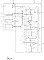
- the driver board 10 comprises a common waveform generator 13 that generates a basic waveform independent of a specific print element.
- Two fixed voltage sources, 14 and 15, are on the board to be used for supplying the extra voltages 4 and 5 in the waveform.
- a print data memory 16 is available for the waveshape selection module 17 that specifies the timing 6 and 7 for tuning the waveform to the individual print elements 23.
- a driver ASIC 11 is positioned as close as possible to the printhead 12 in order to reduce parasitic effects.
- the ASIC 11 comprises a main switch control 20 and a switch module 22 for each print element.
- Each switch module 22 comprises a tune switch control 21 and three transistor switches 31, 32 and 33.
- the main switch control 20 determines from the print data 16, the timing of the first switch 31 for connecting the basic part of the waveform generated by generator 13 to a print element.
- the waveshape selection module 17 supplies the parameters for the tune switch control 21 to determine the timing to bring the switches 32 and 33 from their open, blocking state into a closed, saturation state. These transistors are therefore not operated in a conducting state, which limits the dissipation that they provide.
- the resulting voltage supplied to the print element 23 is a summation of a number of fixed sources controlled by the various switches to obtain an actuation that is individually tunable for each print element.
Landscapes
- Engineering & Computer Science (AREA)
- Microelectronics & Electronic Packaging (AREA)
- Particle Formation And Scattering Control In Inkjet Printers (AREA)
- Ink Jet (AREA)
Description
- This application claims priority to European Patent Application No.
15174229.3, filed on June 29, 2015 16156242.6, filed on February 18, 2016 - The invention relates to an electronic circuit for driving an inkjet print element in an array of print elements with an electric waveform. In particular, the invention relates to a circuit that enables a selection of a tunable waveform in dependence of a print element. Furthermore, the invention relates to a printhead module for jetting ink drops.
- High volume printers which are capable of printing more than 300 A4 size full color pages are known. These employ a single pass inkjet printing process wherein multiple printheads are combined to one page wide printing array to achieve a required performance. A small droplet size (< 10 pl (picoliter)) and a high nozzle density (> 600 npi (nozzles per inch)) are used to obtain a satisfactory print quality.
- Contemporary printheads using piezo-electric actuators in the print elements are operated at jetting frequencies of several tens of kHz. After actuation with an appropriate electric signal, or waveform, the piezo actuator that is mounted to a channel filled with ink, causes a liquid droplet of ink or the like to be discharged from a nozzle at the end of the channel. After an ejection of a droplet the print element is preferably in a condition to eject a further droplet, although it may take some time to stabilize the print element. It is known to add a second part to a waveform to expedite this stabilisation process.
- Droplet uniformity, which relates to variations in a size and a speed of the droplet, depends critically on the geometry and dimensions of the channel and the way it is actuated by the waveform. In particular, the waveform may be tuned to an individual print element by measuring a response to an actuation. This response is obtained either by directly measuring the droplet properties or by determining of the residual ink movement in the channel, such as the position of the meniscus in the nozzle, or by monitoring a dot that results from the droplet reaching a substrate. The electronic circuits that are used to drive a printhead with individual waveforms for each print element, typically use a linear class AB type of amplifiers to generate the actuation waveform.
- For the electronic circuit the piezo-electric actuator behaves in first order as a capacitive load, causing the waveform generator to dissipate an amount of energy proportional to the capacitance and the square of the applied voltage. Since each print element requires a dedicated generator having the ability to tune the waveform to the related element, the power dissipation in the generator increases significantly with an increasing density of print elements in a print head. Thus, there is a problem in obtaining an electronic circuit that is capable of applying an individually tunable waveform for each piezo actuator in a printhead without getting the related power dissipation in the waveform generator.
US-A-2012/262512 discloses the preamble ofclaims 1 and 9. - According to the present invention, there is provided an electronic circuit for driving an inkjet print element in an array of print elements with an electric waveform, a print element comprising a piezo transducer for converting the electric waveform in a mechanical displacement, the electric waveform being tunable for an individual print element, the circuit comprising a common waveform generator that is connected to the piezo transducer through a first print data dependent switch for providing a common electric waveform, independent of the print element, and the circuit further comprising a waveform tuning part, dependent on the print element and the print data, for controlling a second switch that adds electric energy from a fixed voltage source to the electric waveform, wherein the switches are operable in either a saturation state or a blocking state to limit an amount of dissipation in the switches.
- It is well known that a switch in the form of a transistor may operate in three states: a blocking, a conducting and a saturation state. In ordinary driver circuits, an individualized waveform is generated and amplified by transistors in a conducting state in order to obtain a required voltage for delivering energy in the actuator, which causes dissipation in these circuits. In a blocking state, no current is passed to the actuator load, so no dissipation is generated. In a saturation state, no voltage difference across the switch occurs and thus no dissipation is generated. According to the invention, the waveform tuning part is obtained from a fixed voltage source which is switched into connection with the actuator load during a short time of the waveform. Only during the alteration of the voltage across the actuator, power proportional to the square of the voltage difference is dissipated. This voltage difference, stemming from the fixed voltage source, is rather small as it is only related to a tuning part of the complete waveform. The tuning itself is realized by adjusting the amount of time this fixed voltage is applied. Thus the power in the circuit is reduced compared to tuning by voltage adjustment.
- In a preferred embodiment, the fixed voltage source has a lower voltage than the peak voltage from the common waveform generator. Thus electric energy is removed from the capacitive load by teh fixed voltage source. The tuning part then involves only one voltage alteration instead of two, as in the general situation, and the dissipated power in the tuning circuit is reduced by a factor of two.
- In a further embodiment, the tuning part further depends on the print data of neighbouring print elements. With the high integration density, the print elements do not operate completely independently. Thus, the tuning of the waveform may be used to compensate for the possible actuation of neighbouring print elements.
- In a further embodiment, a third switch is provided to the print element for adding electric energy in a second part of the waveform. In addtion to a first switch for applying the fixed waveform for actuating a print element and a second switch for applying a tuning part to a driving pulse of the waveform, a third switch may be used to add electric energy to a part of the waveform that stabilizes the print element. In this case the waveform comprises two pulses of opposite polarity, or in some cases equal polarity, wherein the second part, or brake pulse, is also tuned to perform optimally.
- Further details of the invention are given in the dependent claims. The present invention may also be embodied in a printhead module comprising a printhead chip and a driver board, connected by a module comprising an electronic circuit as described.
- The present invention further comprises a method for adapting an electric waveform according to claim 9.
- A property of the ink drop that is relevant in the print process is its volume velocity, which determines the size of a dot that materializes when the ink drop hits the substrate underneath the print elements. Another property of the ink drop is its velocity. In order to make these properties more uniform across the various print elements in the array, it may be necesssary to tune the electric waveform in the indicated way.
- Further scope of applicability of the present invention will become apparent from the detailed description given hereinafter. However, it should be understood that the detailed description and specific examples, while indicating preferred embodiments of the invention, are given by way of illustration only, since various changes and modifications within the scope of the invention will become apparent to those skilled in the art from this detailed description.
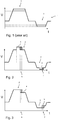
- The present invention will become more fully understood from the detailed description given hereinbelow and the accompanying drawings which are given by way of illustration only, and thus are not limitative of the present invention, and wherein:
- Figure 1
- illustrates a tunable waveform as known in the prior art;
- Figure 2
- shows a tunable waveform according to the present invention;
- Figure 3
- shows a preferred shape of the tunable waveform, and
- Figure 4
- is an embodiment of an electronic circuit that provides the intended tunable waveform.
- The present invention will now be described with reference to the accompanying drawings, wherein the same or similar elements are identified with the same reference numeral.
-
Figure 1 shows awaveform 1 comprising two parts, or two pulses, as is known in the prior art. The waveform takes a time in the order of 5 to 25 us (microseconds) and a maximum voltage is of the order of 30 to 80 V (Volts). Afirst pulse 2, the jet pulse, is applied to a piezo actuator of a print element for ejecting an ink drop from a nozzle in the print element. Asecond pulse 3, the brake pulse, is applied to reduce the residual vibrations of the ink inside the print element. Both pulses are tunable in respect to the maximum voltage to adjust the veloctiy and volume of the ejected droplet and to adjust the effectivity of the brake pulse respectively. It is noted that thewaveform 1 may deform somewhat by the capacitive load of the piezo actuator. -
Figure 2 shows a waveform as applied by the circuit according to the present invention. In this waveform thejet pulse 2 andbrake pulse 3 are composed of a basic part that is independent of the print element. In addition to this basic part anextra voltage 4 and anextra voltage 5 are supplied to the capacitive load. Both extra voltages have avariable duration -
Figure 3 shows a preferred waveform wherein the extra voltage has a lower voltage than the peak voltage from the common waveform generator, both in thejet pulse 2 and in thebrake pulse 3. Since there is only one alteration of the voltage at avariable timing Figure 2 . -
Figure 4 is a printhead module wherein print elements are actuated according to the waveform ofFigure 2 or Figure 3 . It comprises aprinthead driver board 10, adriver ASIC 11 and aprinthead chip 12 comprisingprint elements 23, each print element having a piezo electric actuator for transforming an electric voltage to an acoustic wave in the ink of the element. The piezo actuator is electrically a capacitive load for the electronic circuit. - The
driver board 10 comprises acommon waveform generator 13 that generates a basic waveform independent of a specific print element. Two fixed voltage sources, 14 and 15, are on the board to be used for supplying theextra voltages print data memory 16 is available for thewaveshape selection module 17 that specifies thetiming individual print elements 23. Adriver ASIC 11 is positioned as close as possible to theprinthead 12 in order to reduce parasitic effects. TheASIC 11 comprises amain switch control 20 and a switch module 22 for each print element. Each switch module 22 comprises atune switch control 21 and threetransistor switches main switch control 20 determines from theprint data 16, the timing of thefirst switch 31 for connecting the basic part of the waveform generated bygenerator 13 to a print element. Thewaveshape selection module 17 supplies the parameters for thetune switch control 21 to determine the timing to bring theswitches print element 23 is a summation of a number of fixed sources controlled by the various switches to obtain an actuation that is individually tunable for each print element. - The skilled person will recognise that other embodiments are possible within the scope of the appended claims.
Claims (11)
- An electronic circuit for driving an inkjet print element (23) in an array of print elements with an electric waveform, a print element comprising a piezo transducer for converting the electric waveform in a mechanical displacement, the electric waveform being tuneable for an individual print element, the circuit comprising a common waveform generator (13) that is connected to the piezo transducer through a first print data dependent switch (31) for providing a common electric waveform, (2) independent of the print element, and characterised in that the circuit further comprises a waveform tuning part, dependent on the print element and the print data, for controlling a second switch (32) that adds electric energy (3) from a fixed voltage source to the common electric waveform, wherein the switches are operable in either a saturation state or a blocking state to limit an amount of dissipation in the switches.
- The electronic circuit according to claim 1, wherein the fixed voltage source has a lower voltage than the peak voltage from the common waveform generator.
- The electronic circuit according to claim 1, wherein the tuning part further depends on the print data of neighbouring print elements.
- The electronic circuit according to claim 1, wherein the tuning part depends on the print data associated with previous waveforms.
- The electronic circuit according to claim 1, wherein a third switch is provided to the print element for adding electric energy in a second part of the waveform.
- The electronic circuit according to claim 1, wherein the waveform tuning part comprises timing parameters for controlling the second switch.
- A printhead module comprising a printhead chip and a driver board, connected by a module comprising an electronic circuit according to claim 1, the printhead comprising the array of print elements, the module comprising the switches for applying the electric waveform to the the print elements and the driver board comprising the common waveform generator and the voltage source.
- The printhead module according to claim 7, wherein the driver board comprises a memory for saving waveform tuning parameters for a print element of the array of print elements.
- A method for adapting an electric waveform tunable for an individual print element for actuating a print element in an array of print elements to eject an ink drop, wherein the print element comprises a piezo transducer for converting the electric waveform in a mechanical displacement, the waveform comprising a first pulse independent of the specific print element being provided to the piezo transducer through a first print data dependent switch and characterised in that the waveform further comprises a second pulse dependent on the print element and the print data that is added to the first pulse by controlling a second switch that adds energy from a fixed voltage source to the first pulse, the second pulse having a fixed strength and a tuneable duration, such that a property of the ink drop resulting from the actuation by the electric waveform is varied, wherein the switches are operable in either a saturation state or a blocking state to limit an amount of dissipation in the first and second switches.
- The method according to claim 9, wherein the variable property of the ink drop is the velocity of the ink drop.
- The method according to claim 9, wherein the variable property of the ink drop is the volume of the ink drop.
Applications Claiming Priority (3)
| Application Number | Priority Date | Filing Date | Title |
|---|---|---|---|
| EP15174229 | 2015-06-29 | ||
| EP16156242 | 2016-02-18 | ||
| PCT/EP2016/064527 WO2017001276A1 (en) | 2015-06-29 | 2016-06-23 | Electronic circuit for driving an array of inkjet print elements |
Publications (2)
| Publication Number | Publication Date |
|---|---|
| EP3313665A1 EP3313665A1 (en) | 2018-05-02 |
| EP3313665B1 true EP3313665B1 (en) | 2020-08-19 |
Family
ID=56148426
Family Applications (1)
| Application Number | Title | Priority Date | Filing Date |
|---|---|---|---|
| EP16730862.6A Active EP3313665B1 (en) | 2015-06-29 | 2016-06-23 | Electronic circuit for driving an array of inkjet print elements |
Country Status (4)
| Country | Link |
|---|---|
| US (1) | US10457040B2 (en) |
| EP (1) | EP3313665B1 (en) |
| JP (1) | JP6875298B2 (en) |
| WO (1) | WO2017001276A1 (en) |
Families Citing this family (3)
| Publication number | Priority date | Publication date | Assignee | Title |
|---|---|---|---|---|
| GB2536262B (en) * | 2015-03-11 | 2019-09-25 | Xaar Technology Ltd | Actuator drive circuit with trim control of pulse shape |
| GB2570668A (en) * | 2018-01-31 | 2019-08-07 | Xaar Technology Ltd | Droplet deposition apparatus |
| EP3626455A1 (en) * | 2018-09-20 | 2020-03-25 | Canon Production Printing Holding B.V. | Method for reducing secondary satellites in ink jet printing |
Citations (3)
| Publication number | Priority date | Publication date | Assignee | Title |
|---|---|---|---|---|
| US20070030297A1 (en) * | 2005-06-16 | 2007-02-08 | Toshiba Tec Kabushiki Kaisha | Ink jet head driving method and apparatus |
| US20070076022A1 (en) * | 2005-10-05 | 2007-04-05 | Fuji Xerox Co., Ltd. | Driving circuit of a piezoelectric element, and liquid droplet ejecting device |
| US20150072458A1 (en) * | 2012-06-06 | 2015-03-12 | Panasonic Corporation | Inkjet device and manufacturing method for organic el device |
Family Cites Families (13)
| Publication number | Priority date | Publication date | Assignee | Title |
|---|---|---|---|---|
| US4369455A (en) * | 1980-12-08 | 1983-01-18 | Hewlett-Packard Company | Ink jet printer drive pulse for elimination of multiple ink droplet ejection |
| US5475405A (en) * | 1993-12-14 | 1995-12-12 | Hewlett-Packard Company | Control circuit for regulating temperature in an ink-jet print head |
| JP3116886B2 (en) * | 1998-01-16 | 2000-12-11 | 日本電気株式会社 | Piezo drive circuit |
| JP2000037861A (en) * | 1998-07-24 | 2000-02-08 | Brother Ind Ltd | Ink jet recording device |
| DE60204180T2 (en) * | 2001-03-09 | 2005-10-20 | Seiko Epson Corp. | A liquid jet device and method of controlling the same |
| JP4152757B2 (en) * | 2002-01-28 | 2008-09-17 | シャープ株式会社 | Capacitive load driving circuit, capacitive load driving method, and apparatus using the same |
| JP2004025681A (en) * | 2002-06-26 | 2004-01-29 | Seiko Epson Corp | Liquid jet |
| US7234788B2 (en) * | 2004-11-03 | 2007-06-26 | Dimatix, Inc. | Individual voltage trimming with waveforms |
| JP2011218745A (en) * | 2010-04-14 | 2011-11-04 | Seiko Epson Corp | Capacitive load driving circuit |
| JP2012223936A (en) * | 2011-04-18 | 2012-11-15 | Seiko Epson Corp | Piezoelectric element drive circuit, and fluid ejection device |
| US20150054867A1 (en) * | 2012-04-25 | 2015-02-26 | Hewlett-Packard Development Company, L.P. | Print nozzle amplifier with capacitive feedback |
| US8926041B2 (en) * | 2013-01-28 | 2015-01-06 | Fujifilm Dimatix, Inc. | Ink jetting |
| GB2530976B (en) * | 2014-09-10 | 2017-05-03 | Xaar Technology Ltd | Setting start voltage for driving actuating elements |
-
2016
- 2016-06-23 WO PCT/EP2016/064527 patent/WO2017001276A1/en not_active Ceased
- 2016-06-23 EP EP16730862.6A patent/EP3313665B1/en active Active
- 2016-06-23 JP JP2017565165A patent/JP6875298B2/en active Active
-
2017
- 2017-12-21 US US15/850,089 patent/US10457040B2/en active Active
Patent Citations (3)
| Publication number | Priority date | Publication date | Assignee | Title |
|---|---|---|---|---|
| US20070030297A1 (en) * | 2005-06-16 | 2007-02-08 | Toshiba Tec Kabushiki Kaisha | Ink jet head driving method and apparatus |
| US20070076022A1 (en) * | 2005-10-05 | 2007-04-05 | Fuji Xerox Co., Ltd. | Driving circuit of a piezoelectric element, and liquid droplet ejecting device |
| US20150072458A1 (en) * | 2012-06-06 | 2015-03-12 | Panasonic Corporation | Inkjet device and manufacturing method for organic el device |
Also Published As
| Publication number | Publication date |
|---|---|
| JP2018519191A (en) | 2018-07-19 |
| US20180111369A1 (en) | 2018-04-26 |
| US10457040B2 (en) | 2019-10-29 |
| WO2017001276A1 (en) | 2017-01-05 |
| JP6875298B2 (en) | 2021-05-19 |
| EP3313665A1 (en) | 2018-05-02 |
Similar Documents
| Publication | Publication Date | Title |
|---|---|---|
| EP3431294B1 (en) | Fluidic die | |
| EP1814738B1 (en) | Print systems and techniques | |
| EP1833677B1 (en) | Individual voltage trimming with waveforms | |
| KR20110133192A (en) | Inkjet head drive | |
| US10457040B2 (en) | Electronic circuit for driving an array of inkjet print elements | |
| CN111634121B (en) | Liquid jets and printers | |
| JP2018149768A (en) | Inkjet head and inkjet recording apparatus | |
| JP7012436B2 (en) | Inkjet head | |
| JP6450533B2 (en) | Inkjet head and inkjet printer | |
| EP1985451B1 (en) | Method of driving an ink-jet head, ink-jet head, and ink-jet recording apparatus | |
| US20040066425A1 (en) | Liquid ejecting apparatus | |
| US6805420B2 (en) | Drive unit for liquid ejection head and liquid ejection apparatus provided with such unit | |
| US20180272698A1 (en) | Inkjet head, inkjet recording apparatus, and discharging method | |
| JP2004042414A (en) | Driving method of inkjet head and inkjet printing apparatus using the driving method | |
| JP2010105300A (en) | Liquid discharge apparatus | |
| JP7458914B2 (en) | Liquid ejection head and printer | |
| US12558887B2 (en) | Circuit and method for driving a print head | |
| JP7242940B2 (en) | Liquid ejection head and printer | |
| JP4763418B2 (en) | Ink jet head driving method, ink jet head, and ink jet recording apparatus | |
| JP2020055214A (en) | Liquid discharge head and printer | |
| JP2020055213A (en) | Liquid discharge head | |
| JP2007125748A (en) | Inkjet recorder | |
| JP2010099982A (en) | Fluid jetting apparatus | |
| JP2020152070A (en) | Liquid discharge head and liquid discharge device |
Legal Events
| Date | Code | Title | Description |
|---|---|---|---|
| STAA | Information on the status of an ep patent application or granted ep patent |
Free format text: STATUS: THE INTERNATIONAL PUBLICATION HAS BEEN MADE |
|
| PUAI | Public reference made under article 153(3) epc to a published international application that has entered the european phase |
Free format text: ORIGINAL CODE: 0009012 |
|
| STAA | Information on the status of an ep patent application or granted ep patent |
Free format text: STATUS: REQUEST FOR EXAMINATION WAS MADE |
|
| 17P | Request for examination filed |
Effective date: 20180129 |
|
| AK | Designated contracting states |
Kind code of ref document: A1 Designated state(s): AL AT BE BG CH CY CZ DE DK EE ES FI FR GB GR HR HU IE IS IT LI LT LU LV MC MK MT NL NO PL PT RO RS SE SI SK SM TR |
|
| AX | Request for extension of the european patent |
Extension state: BA ME |
|
| DAV | Request for validation of the european patent (deleted) | ||
| DAX | Request for extension of the european patent (deleted) | ||
| STAA | Information on the status of an ep patent application or granted ep patent |
Free format text: STATUS: EXAMINATION IS IN PROGRESS |
|
| 17Q | First examination report despatched |
Effective date: 20190614 |
|
| GRAP | Despatch of communication of intention to grant a patent |
Free format text: ORIGINAL CODE: EPIDOSNIGR1 |
|
| STAA | Information on the status of an ep patent application or granted ep patent |
Free format text: STATUS: GRANT OF PATENT IS INTENDED |
|
| RAP1 | Party data changed (applicant data changed or rights of an application transferred) |
Owner name: CANON PRODUCTION PRINTING NETHERLANDS B.V. |
|
| INTG | Intention to grant announced |
Effective date: 20200318 |
|
| GRAS | Grant fee paid |
Free format text: ORIGINAL CODE: EPIDOSNIGR3 |
|
| GRAA | (expected) grant |
Free format text: ORIGINAL CODE: 0009210 |
|
| STAA | Information on the status of an ep patent application or granted ep patent |
Free format text: STATUS: THE PATENT HAS BEEN GRANTED |
|
| AK | Designated contracting states |
Kind code of ref document: B1 Designated state(s): AL AT BE BG CH CY CZ DE DK EE ES FI FR GB GR HR HU IE IS IT LI LT LU LV MC MK MT NL NO PL PT RO RS SE SI SK SM TR |
|
| REG | Reference to a national code |
Ref country code: CH Ref legal event code: EP |
|
| REG | Reference to a national code |
Ref country code: DE Ref legal event code: R096 Ref document number: 602016042257 Country of ref document: DE |
|
| REG | Reference to a national code |
Ref country code: AT Ref legal event code: REF Ref document number: 1303500 Country of ref document: AT Kind code of ref document: T Effective date: 20200915 |
|
| REG | Reference to a national code |
Ref country code: IE Ref legal event code: FG4D |
|
| REG | Reference to a national code |
Ref country code: NL Ref legal event code: FP |
|
| RAP2 | Party data changed (patent owner data changed or rights of a patent transferred) |
Owner name: CANON PRODUCTION PRINTING NETHERLANDS B.V. |
|
| REG | Reference to a national code |
Ref country code: LT Ref legal event code: MG4D |
|
| PG25 | Lapsed in a contracting state [announced via postgrant information from national office to epo] |
Ref country code: GR Free format text: LAPSE BECAUSE OF FAILURE TO SUBMIT A TRANSLATION OF THE DESCRIPTION OR TO PAY THE FEE WITHIN THE PRESCRIBED TIME-LIMIT Effective date: 20201120 Ref country code: FI Free format text: LAPSE BECAUSE OF FAILURE TO SUBMIT A TRANSLATION OF THE DESCRIPTION OR TO PAY THE FEE WITHIN THE PRESCRIBED TIME-LIMIT Effective date: 20200819 Ref country code: HR Free format text: LAPSE BECAUSE OF FAILURE TO SUBMIT A TRANSLATION OF THE DESCRIPTION OR TO PAY THE FEE WITHIN THE PRESCRIBED TIME-LIMIT Effective date: 20200819 Ref country code: SE Free format text: LAPSE BECAUSE OF FAILURE TO SUBMIT A TRANSLATION OF THE DESCRIPTION OR TO PAY THE FEE WITHIN THE PRESCRIBED TIME-LIMIT Effective date: 20200819 Ref country code: NO Free format text: LAPSE BECAUSE OF FAILURE TO SUBMIT A TRANSLATION OF THE DESCRIPTION OR TO PAY THE FEE WITHIN THE PRESCRIBED TIME-LIMIT Effective date: 20201119 Ref country code: BG Free format text: LAPSE BECAUSE OF FAILURE TO SUBMIT A TRANSLATION OF THE DESCRIPTION OR TO PAY THE FEE WITHIN THE PRESCRIBED TIME-LIMIT Effective date: 20201119 Ref country code: LT Free format text: LAPSE BECAUSE OF FAILURE TO SUBMIT A TRANSLATION OF THE DESCRIPTION OR TO PAY THE FEE WITHIN THE PRESCRIBED TIME-LIMIT Effective date: 20200819 Ref country code: PT Free format text: LAPSE BECAUSE OF FAILURE TO SUBMIT A TRANSLATION OF THE DESCRIPTION OR TO PAY THE FEE WITHIN THE PRESCRIBED TIME-LIMIT Effective date: 20201221 |
|
| REG | Reference to a national code |
Ref country code: AT Ref legal event code: MK05 Ref document number: 1303500 Country of ref document: AT Kind code of ref document: T Effective date: 20200819 |
|
| PG25 | Lapsed in a contracting state [announced via postgrant information from national office to epo] |
Ref country code: PL Free format text: LAPSE BECAUSE OF FAILURE TO SUBMIT A TRANSLATION OF THE DESCRIPTION OR TO PAY THE FEE WITHIN THE PRESCRIBED TIME-LIMIT Effective date: 20200819 Ref country code: RS Free format text: LAPSE BECAUSE OF FAILURE TO SUBMIT A TRANSLATION OF THE DESCRIPTION OR TO PAY THE FEE WITHIN THE PRESCRIBED TIME-LIMIT Effective date: 20200819 Ref country code: LV Free format text: LAPSE BECAUSE OF FAILURE TO SUBMIT A TRANSLATION OF THE DESCRIPTION OR TO PAY THE FEE WITHIN THE PRESCRIBED TIME-LIMIT Effective date: 20200819 Ref country code: IS Free format text: LAPSE BECAUSE OF FAILURE TO SUBMIT A TRANSLATION OF THE DESCRIPTION OR TO PAY THE FEE WITHIN THE PRESCRIBED TIME-LIMIT Effective date: 20201219 |
|
| PG25 | Lapsed in a contracting state [announced via postgrant information from national office to epo] |
Ref country code: EE Free format text: LAPSE BECAUSE OF FAILURE TO SUBMIT A TRANSLATION OF THE DESCRIPTION OR TO PAY THE FEE WITHIN THE PRESCRIBED TIME-LIMIT Effective date: 20200819 Ref country code: CZ Free format text: LAPSE BECAUSE OF FAILURE TO SUBMIT A TRANSLATION OF THE DESCRIPTION OR TO PAY THE FEE WITHIN THE PRESCRIBED TIME-LIMIT Effective date: 20200819 Ref country code: DK Free format text: LAPSE BECAUSE OF FAILURE TO SUBMIT A TRANSLATION OF THE DESCRIPTION OR TO PAY THE FEE WITHIN THE PRESCRIBED TIME-LIMIT Effective date: 20200819 Ref country code: SM Free format text: LAPSE BECAUSE OF FAILURE TO SUBMIT A TRANSLATION OF THE DESCRIPTION OR TO PAY THE FEE WITHIN THE PRESCRIBED TIME-LIMIT Effective date: 20200819 Ref country code: RO Free format text: LAPSE BECAUSE OF FAILURE TO SUBMIT A TRANSLATION OF THE DESCRIPTION OR TO PAY THE FEE WITHIN THE PRESCRIBED TIME-LIMIT Effective date: 20200819 |
|
| REG | Reference to a national code |
Ref country code: DE Ref legal event code: R097 Ref document number: 602016042257 Country of ref document: DE |
|
| PG25 | Lapsed in a contracting state [announced via postgrant information from national office to epo] |
Ref country code: AT Free format text: LAPSE BECAUSE OF FAILURE TO SUBMIT A TRANSLATION OF THE DESCRIPTION OR TO PAY THE FEE WITHIN THE PRESCRIBED TIME-LIMIT Effective date: 20200819 Ref country code: AL Free format text: LAPSE BECAUSE OF FAILURE TO SUBMIT A TRANSLATION OF THE DESCRIPTION OR TO PAY THE FEE WITHIN THE PRESCRIBED TIME-LIMIT Effective date: 20200819 Ref country code: ES Free format text: LAPSE BECAUSE OF FAILURE TO SUBMIT A TRANSLATION OF THE DESCRIPTION OR TO PAY THE FEE WITHIN THE PRESCRIBED TIME-LIMIT Effective date: 20200819 |
|
| PLBE | No opposition filed within time limit |
Free format text: ORIGINAL CODE: 0009261 |
|
| STAA | Information on the status of an ep patent application or granted ep patent |
Free format text: STATUS: NO OPPOSITION FILED WITHIN TIME LIMIT |
|
| PG25 | Lapsed in a contracting state [announced via postgrant information from national office to epo] |
Ref country code: SK Free format text: LAPSE BECAUSE OF FAILURE TO SUBMIT A TRANSLATION OF THE DESCRIPTION OR TO PAY THE FEE WITHIN THE PRESCRIBED TIME-LIMIT Effective date: 20200819 |
|
| 26N | No opposition filed |
Effective date: 20210520 |
|
| PG25 | Lapsed in a contracting state [announced via postgrant information from national office to epo] |
Ref country code: IT Free format text: LAPSE BECAUSE OF FAILURE TO SUBMIT A TRANSLATION OF THE DESCRIPTION OR TO PAY THE FEE WITHIN THE PRESCRIBED TIME-LIMIT Effective date: 20200819 |
|
| PG25 | Lapsed in a contracting state [announced via postgrant information from national office to epo] |
Ref country code: SI Free format text: LAPSE BECAUSE OF FAILURE TO SUBMIT A TRANSLATION OF THE DESCRIPTION OR TO PAY THE FEE WITHIN THE PRESCRIBED TIME-LIMIT Effective date: 20200819 |
|
| PG25 | Lapsed in a contracting state [announced via postgrant information from national office to epo] |
Ref country code: MC Free format text: LAPSE BECAUSE OF FAILURE TO SUBMIT A TRANSLATION OF THE DESCRIPTION OR TO PAY THE FEE WITHIN THE PRESCRIBED TIME-LIMIT Effective date: 20200819 |
|
| REG | Reference to a national code |
Ref country code: CH Ref legal event code: PL |
|
| REG | Reference to a national code |
Ref country code: BE Ref legal event code: MM Effective date: 20210630 |
|
| PG25 | Lapsed in a contracting state [announced via postgrant information from national office to epo] |
Ref country code: LU Free format text: LAPSE BECAUSE OF NON-PAYMENT OF DUE FEES Effective date: 20210623 |
|
| PG25 | Lapsed in a contracting state [announced via postgrant information from national office to epo] |
Ref country code: LI Free format text: LAPSE BECAUSE OF NON-PAYMENT OF DUE FEES Effective date: 20210630 Ref country code: IE Free format text: LAPSE BECAUSE OF NON-PAYMENT OF DUE FEES Effective date: 20210623 Ref country code: CH Free format text: LAPSE BECAUSE OF NON-PAYMENT OF DUE FEES Effective date: 20210630 |
|
| PG25 | Lapsed in a contracting state [announced via postgrant information from national office to epo] |
Ref country code: BE Free format text: LAPSE BECAUSE OF NON-PAYMENT OF DUE FEES Effective date: 20210630 |
|
| PG25 | Lapsed in a contracting state [announced via postgrant information from national office to epo] |
Ref country code: CY Free format text: LAPSE BECAUSE OF FAILURE TO SUBMIT A TRANSLATION OF THE DESCRIPTION OR TO PAY THE FEE WITHIN THE PRESCRIBED TIME-LIMIT Effective date: 20200819 |
|
| PG25 | Lapsed in a contracting state [announced via postgrant information from national office to epo] |
Ref country code: HU Free format text: LAPSE BECAUSE OF FAILURE TO SUBMIT A TRANSLATION OF THE DESCRIPTION OR TO PAY THE FEE WITHIN THE PRESCRIBED TIME-LIMIT; INVALID AB INITIO Effective date: 20160623 |
|
| PG25 | Lapsed in a contracting state [announced via postgrant information from national office to epo] |
Ref country code: MK Free format text: LAPSE BECAUSE OF FAILURE TO SUBMIT A TRANSLATION OF THE DESCRIPTION OR TO PAY THE FEE WITHIN THE PRESCRIBED TIME-LIMIT Effective date: 20200819 |
|
| PG25 | Lapsed in a contracting state [announced via postgrant information from national office to epo] |
Ref country code: TR Free format text: LAPSE BECAUSE OF FAILURE TO SUBMIT A TRANSLATION OF THE DESCRIPTION OR TO PAY THE FEE WITHIN THE PRESCRIBED TIME-LIMIT Effective date: 20200819 |
|
| PG25 | Lapsed in a contracting state [announced via postgrant information from national office to epo] |
Ref country code: MT Free format text: LAPSE BECAUSE OF FAILURE TO SUBMIT A TRANSLATION OF THE DESCRIPTION OR TO PAY THE FEE WITHIN THE PRESCRIBED TIME-LIMIT Effective date: 20200819 |
|
| PGFP | Annual fee paid to national office [announced via postgrant information from national office to epo] |
Ref country code: NL Payment date: 20250519 Year of fee payment: 10 |
|
| PGFP | Annual fee paid to national office [announced via postgrant information from national office to epo] |
Ref country code: DE Payment date: 20250618 Year of fee payment: 10 |
|
| PGFP | Annual fee paid to national office [announced via postgrant information from national office to epo] |
Ref country code: GB Payment date: 20250618 Year of fee payment: 10 |
|
| PGFP | Annual fee paid to national office [announced via postgrant information from national office to epo] |
Ref country code: FR Payment date: 20250625 Year of fee payment: 10 |