EP3312884A1 - Fin-fet devices and fabrication methods thereof - Google Patents
Fin-fet devices and fabrication methods thereof Download PDFInfo
- Publication number
- EP3312884A1 EP3312884A1 EP17196527.0A EP17196527A EP3312884A1 EP 3312884 A1 EP3312884 A1 EP 3312884A1 EP 17196527 A EP17196527 A EP 17196527A EP 3312884 A1 EP3312884 A1 EP 3312884A1
- Authority
- EP
- European Patent Office
- Prior art keywords
- layer
- fin
- forming
- structures
- gate structures
- Prior art date
- Legal status (The legal status is an assumption and is not a legal conclusion. Google has not performed a legal analysis and makes no representation as to the accuracy of the status listed.)
- Withdrawn
Links
Images



Classifications
-
- H—ELECTRICITY
- H10—SEMICONDUCTOR DEVICES; ELECTRIC SOLID-STATE DEVICES NOT OTHERWISE PROVIDED FOR
- H10D—INORGANIC ELECTRIC SEMICONDUCTOR DEVICES
- H10D84/00—Integrated devices formed in or on semiconductor substrates that comprise only semiconducting layers, e.g. on Si wafers or on GaAs-on-Si wafers
- H10D84/01—Manufacture or treatment
- H10D84/02—Manufacture or treatment characterised by using material-based technologies
- H10D84/03—Manufacture or treatment characterised by using material-based technologies using Group IV technology, e.g. silicon technology or silicon-carbide [SiC] technology
- H10D84/038—Manufacture or treatment characterised by using material-based technologies using Group IV technology, e.g. silicon technology or silicon-carbide [SiC] technology using silicon technology, e.g. SiGe
-
- H—ELECTRICITY
- H10—SEMICONDUCTOR DEVICES; ELECTRIC SOLID-STATE DEVICES NOT OTHERWISE PROVIDED FOR
- H10D—INORGANIC ELECTRIC SEMICONDUCTOR DEVICES
- H10D30/00—Field-effect transistors [FET]
- H10D30/01—Manufacture or treatment
- H10D30/021—Manufacture or treatment of FETs having insulated gates [IGFET]
- H10D30/024—Manufacture or treatment of FETs having insulated gates [IGFET] of fin field-effect transistors [FinFET]
-
- H—ELECTRICITY
- H10—SEMICONDUCTOR DEVICES; ELECTRIC SOLID-STATE DEVICES NOT OTHERWISE PROVIDED FOR
- H10D—INORGANIC ELECTRIC SEMICONDUCTOR DEVICES
- H10D30/00—Field-effect transistors [FET]
- H10D30/60—Insulated-gate field-effect transistors [IGFET]
- H10D30/62—Fin field-effect transistors [FinFET]
-
- H—ELECTRICITY
- H10—SEMICONDUCTOR DEVICES; ELECTRIC SOLID-STATE DEVICES NOT OTHERWISE PROVIDED FOR
- H10D—INORGANIC ELECTRIC SEMICONDUCTOR DEVICES
- H10D30/00—Field-effect transistors [FET]
- H10D30/60—Insulated-gate field-effect transistors [IGFET]
- H10D30/62—Fin field-effect transistors [FinFET]
- H10D30/6219—Fin field-effect transistors [FinFET] characterised by the source or drain electrodes
-
- H—ELECTRICITY
- H10—SEMICONDUCTOR DEVICES; ELECTRIC SOLID-STATE DEVICES NOT OTHERWISE PROVIDED FOR
- H10D—INORGANIC ELECTRIC SEMICONDUCTOR DEVICES
- H10D64/00—Electrodes of devices having potential barriers
- H10D64/01—Manufacture or treatment
- H10D64/017—Manufacture or treatment using dummy gates in processes wherein at least parts of the final gates are self-aligned to the dummy gates, i.e. replacement gate processes
-
- H—ELECTRICITY
- H10—SEMICONDUCTOR DEVICES; ELECTRIC SOLID-STATE DEVICES NOT OTHERWISE PROVIDED FOR
- H10D—INORGANIC ELECTRIC SEMICONDUCTOR DEVICES
- H10D64/00—Electrodes of devices having potential barriers
- H10D64/20—Electrodes characterised by their shapes, relative sizes or dispositions
- H10D64/27—Electrodes not carrying the current to be rectified, amplified, oscillated or switched, e.g. gates
- H10D64/311—Gate electrodes for field-effect devices
- H10D64/411—Gate electrodes for field-effect devices for FETs
- H10D64/511—Gate electrodes for field-effect devices for FETs for IGFETs
-
- H—ELECTRICITY
- H10—SEMICONDUCTOR DEVICES; ELECTRIC SOLID-STATE DEVICES NOT OTHERWISE PROVIDED FOR
- H10D—INORGANIC ELECTRIC SEMICONDUCTOR DEVICES
- H10D84/00—Integrated devices formed in or on semiconductor substrates that comprise only semiconducting layers, e.g. on Si wafers or on GaAs-on-Si wafers
- H10D84/01—Manufacture or treatment
- H10D84/0123—Integrating together multiple components covered by H10D12/00 or H10D30/00, e.g. integrating multiple IGBTs
- H10D84/0126—Integrating together multiple components covered by H10D12/00 or H10D30/00, e.g. integrating multiple IGBTs the components including insulated gates, e.g. IGFETs
- H10D84/0165—Integrating together multiple components covered by H10D12/00 or H10D30/00, e.g. integrating multiple IGBTs the components including insulated gates, e.g. IGFETs the components including complementary IGFETs, e.g. CMOS devices
- H10D84/017—Manufacturing their source or drain regions, e.g. silicided source or drain regions
-
- H—ELECTRICITY
- H10—SEMICONDUCTOR DEVICES; ELECTRIC SOLID-STATE DEVICES NOT OTHERWISE PROVIDED FOR
- H10D—INORGANIC ELECTRIC SEMICONDUCTOR DEVICES
- H10D84/00—Integrated devices formed in or on semiconductor substrates that comprise only semiconducting layers, e.g. on Si wafers or on GaAs-on-Si wafers
- H10D84/01—Manufacture or treatment
- H10D84/0123—Integrating together multiple components covered by H10D12/00 or H10D30/00, e.g. integrating multiple IGBTs
- H10D84/0126—Integrating together multiple components covered by H10D12/00 or H10D30/00, e.g. integrating multiple IGBTs the components including insulated gates, e.g. IGFETs
- H10D84/0165—Integrating together multiple components covered by H10D12/00 or H10D30/00, e.g. integrating multiple IGBTs the components including insulated gates, e.g. IGFETs the components including complementary IGFETs, e.g. CMOS devices
- H10D84/0184—Manufacturing their gate sidewall spacers
-
- H—ELECTRICITY
- H10—SEMICONDUCTOR DEVICES; ELECTRIC SOLID-STATE DEVICES NOT OTHERWISE PROVIDED FOR
- H10D—INORGANIC ELECTRIC SEMICONDUCTOR DEVICES
- H10D84/00—Integrated devices formed in or on semiconductor substrates that comprise only semiconducting layers, e.g. on Si wafers or on GaAs-on-Si wafers
- H10D84/01—Manufacture or treatment
- H10D84/0123—Integrating together multiple components covered by H10D12/00 or H10D30/00, e.g. integrating multiple IGBTs
- H10D84/0126—Integrating together multiple components covered by H10D12/00 or H10D30/00, e.g. integrating multiple IGBTs the components including insulated gates, e.g. IGFETs
- H10D84/0165—Integrating together multiple components covered by H10D12/00 or H10D30/00, e.g. integrating multiple IGBTs the components including insulated gates, e.g. IGFETs the components including complementary IGFETs, e.g. CMOS devices
- H10D84/0186—Manufacturing their interconnections or electrodes, e.g. source or drain electrodes
-
- H—ELECTRICITY
- H10—SEMICONDUCTOR DEVICES; ELECTRIC SOLID-STATE DEVICES NOT OTHERWISE PROVIDED FOR
- H10D—INORGANIC ELECTRIC SEMICONDUCTOR DEVICES
- H10D84/00—Integrated devices formed in or on semiconductor substrates that comprise only semiconducting layers, e.g. on Si wafers or on GaAs-on-Si wafers
- H10D84/01—Manufacture or treatment
- H10D84/0123—Integrating together multiple components covered by H10D12/00 or H10D30/00, e.g. integrating multiple IGBTs
- H10D84/0126—Integrating together multiple components covered by H10D12/00 or H10D30/00, e.g. integrating multiple IGBTs the components including insulated gates, e.g. IGFETs
- H10D84/0165—Integrating together multiple components covered by H10D12/00 or H10D30/00, e.g. integrating multiple IGBTs the components including insulated gates, e.g. IGFETs the components including complementary IGFETs, e.g. CMOS devices
- H10D84/0188—Manufacturing their isolation regions
-
- H—ELECTRICITY
- H10—SEMICONDUCTOR DEVICES; ELECTRIC SOLID-STATE DEVICES NOT OTHERWISE PROVIDED FOR
- H10D—INORGANIC ELECTRIC SEMICONDUCTOR DEVICES
- H10D84/00—Integrated devices formed in or on semiconductor substrates that comprise only semiconducting layers, e.g. on Si wafers or on GaAs-on-Si wafers
- H10D84/01—Manufacture or treatment
- H10D84/0123—Integrating together multiple components covered by H10D12/00 or H10D30/00, e.g. integrating multiple IGBTs
- H10D84/0126—Integrating together multiple components covered by H10D12/00 or H10D30/00, e.g. integrating multiple IGBTs the components including insulated gates, e.g. IGFETs
- H10D84/0165—Integrating together multiple components covered by H10D12/00 or H10D30/00, e.g. integrating multiple IGBTs the components including insulated gates, e.g. IGFETs the components including complementary IGFETs, e.g. CMOS devices
- H10D84/0193—Integrating together multiple components covered by H10D12/00 or H10D30/00, e.g. integrating multiple IGBTs the components including insulated gates, e.g. IGFETs the components including complementary IGFETs, e.g. CMOS devices the components including FinFETs
-
- H—ELECTRICITY
- H10—SEMICONDUCTOR DEVICES; ELECTRIC SOLID-STATE DEVICES NOT OTHERWISE PROVIDED FOR
- H10D—INORGANIC ELECTRIC SEMICONDUCTOR DEVICES
- H10D84/00—Integrated devices formed in or on semiconductor substrates that comprise only semiconducting layers, e.g. on Si wafers or on GaAs-on-Si wafers
- H10D84/80—Integrated devices formed in or on semiconductor substrates that comprise only semiconducting layers, e.g. on Si wafers or on GaAs-on-Si wafers characterised by the integration of at least one component covered by groups H10D12/00 or H10D30/00, e.g. integration of IGFETs
- H10D84/82—Integrated devices formed in or on semiconductor substrates that comprise only semiconducting layers, e.g. on Si wafers or on GaAs-on-Si wafers characterised by the integration of at least one component covered by groups H10D12/00 or H10D30/00, e.g. integration of IGFETs of only field-effect components
- H10D84/83—Integrated devices formed in or on semiconductor substrates that comprise only semiconducting layers, e.g. on Si wafers or on GaAs-on-Si wafers characterised by the integration of at least one component covered by groups H10D12/00 or H10D30/00, e.g. integration of IGFETs of only field-effect components of only insulated-gate FETs [IGFET]
- H10D84/85—Complementary IGFETs, e.g. CMOS
- H10D84/853—Complementary IGFETs, e.g. CMOS comprising FinFETs
-
- H—ELECTRICITY
- H10—SEMICONDUCTOR DEVICES; ELECTRIC SOLID-STATE DEVICES NOT OTHERWISE PROVIDED FOR
- H10W—GENERIC PACKAGES, INTERCONNECTIONS, CONNECTORS OR OTHER CONSTRUCTIONAL DETAILS OF DEVICES COVERED BY CLASS H10
- H10W20/00—Interconnections in chips, wafers or substrates
- H10W20/01—Manufacture or treatment
- H10W20/031—Manufacture or treatment of conductive parts of the interconnections
- H10W20/069—Manufacture or treatment of conductive parts of the interconnections by forming self-aligned vias or self-aligned contact plugs
Definitions
- the present invention generally relates to the field of semiconductor fabrication technology and, more particularly, relates to Fin-FET devices and fabrication methods thereof.
- a metal silicide fabrication method may be introduced.
- the metal silicide may have a relatively low resistivity, and thus the contact resistance at the source/drain electrodes may be significantly reduced.
- metal silicide, self-aligned metal silicide, as well as the corresponding formation processes have been widely used to reduce the surface resistance and the contact resistance of the source electrodes and the drain electrodes, and thus may reduce the resistance-capacitation delay (RC delay).
- RC delay resistance-capacitation delay
- SiNi x is usually used to form the metal silicide.
- the metal silicide formed using the SiNi x may demonstrate advanced properties including low contact resistance, low silicon consumption, etc. and may also be able to easily reach a relatively narrow line width. Therefore, SiNi x is regarded as an ideal metal silicide.
- Fin-FET fin field-effect transistor
- a first aspect of the present invention includes a method for fabricating a Fin-FET device.
- the method includes forming a plurality of fin structures on a substrate, forming an isolation structure on the substrate to cover a portion of sidewall surfaces of the fin structures, forming a plurality of gate structures on the isolation layer across the fin structures and covering a portion of sidewall and top surfaces of the fin structures, forming doped source/drain regions in the fin structures on two opposite sides of each gate structure, forming a metal layer on top surfaces of the doped source/drain regions and the gate structures, and performing a reaction annealing process on the metal layer to convert the portion of the metal layer formed on the doped source/drain regions into a metal contact layer.
- the fabrication method further includes removing the unreacted portion of the metal layer after the reaction annealing process, forming a dielectric layer on the metal contact layer and the gate structures with a top surface higher than the top surfaces of the gate structures, forming a plurality of vias through the dielectric layer to expose a portion of the metal contact layer, and forming a plurality of conductive plugs by filling up the vias.
- the metal layer covers entire surfaces of the doped source/drain regions.
- the metal layer is made of one or more of Ni, W, Ti, Ta, Pt, and Co.
- the reaction annealing process performed to convert the metal layer into the metal contact layer is a laser annealing process.
- an anneal temperature used in the laser annealing process is in a range of approximately 800 °C to 880 °C.
- the metal layer is also formed above the isolation structure, and accordingly: after the reaction annealing process, a portion of the metal layer formed above the isolation structure and the gate structures is unreacted; and the unreacted portion of the metal layer formed above the isolation structure and the gate structures is removed by a wet etching process.
- the gate structures are metal gate structures.
- the gate structures are formed after forming the doped source/drain regions.
- forming the gate structures and the doped source/drain regions further includes: forming a plurality of dummy gate structures on the isolation structure across the fin structures with a sidewall spacer formed on sidewall surfaces of each dummy gate structures, wherein the dummy gate structures cover a portion of the sidewall and the top surfaces of the fin structures; forming the doped source/drain regions in the fin structures on two opposite sides of each dummy gate structure; forming a dummy dielectric layer on the doped source/drain regions and the sidewall surfaces of the dummy gate structures, wherein the dummy dielectric layer exposes top surfaces of the dummy gate structures; removing each dummy gate structure to form a trench in the dummy dielectric layer; forming a high-k dielectric layer on sidewall and bottom surfaces of each trench; and forming a gate electrode on the high-k dielectric layer to fill up each trench.
- the thickness of the cap layer is in a range of approximately 5 ⁇ to 35 ⁇ .
- the cap layer is made of one of SiNx and BN.
- a portion of the metal layer is formed on each cap layer.
- the portion of the metal layer formed on each cap layer is removed.
- a repair annealing process is performed on the high-k dielectric layer, and the anneal temperature in the repair annealing process is higher than an anneal temperature of the reaction annealing process.
- the gate structures are metal gate structures and the doped source/drain regions are formed after forming the gate structures.
- a cap layer is formed on a top surface of each gate structure.
- removing the unreacted portion of the metal layer includes removing a portion of the metal layer formed on each cap layer.
- the gate structures are polycrystalline silicon gate structures and the doped source/drain regions are formed after forming the gate structures.
- the reaction annealing process converts a portion of the metal layer formed on the gate structures into a metal contact layer.
- a plurality of sidewall spacers covering sidewall surfaces of the gate structures are formed prior to forming the metal layer on the top surfaces of the doped source/drain regions and the gate structures.
- the metal layer is also formed on the sidewall spacers.
- a protective layer is formed on the metal layer.
- the protective layer is removed.
- the Fin-FET device includes a plurality of N-type metal-oxide-semiconductor (NMOS) transistors, P-type metal-oxide-semiconductor (PMOS) transistors, and complementary metal-oxide-semiconductor (CMOS) transistors.
- NMOS N-type metal-oxide-semiconductor
- PMOS P-type metal-oxide-semiconductor
- CMOS complementary metal-oxide-semiconductor
- the dielectric layer includes a first dielectric layer and a second dielectric layer formed on the second dielectric layer.
- a density of the first dielectric layer is larger than a density of the second dielectric layer.
- forming the first dielectric layer and the second dielectric layer includes: forming the first dielectric layer with a top surface leveled with the top surfaces of the gate structures through a high-density plasma deposition process; forming the second dielectric layer on the first dielectric layer through a plasma-enhanced tetraethyl orthosilication (PETEOS) process.
- PETEOS plasma-enhanced tetraethyl orthosilication
- forming the doped source/drain regions includes: forming an opening in the fin structures next to each sidewall spacer; and forming a stress layer to fill up each opening, wherein: the doped source/drain regions are formed by an in-situ ion implantation process performed during forming the stress layer or by an ion implantation process performed on the stress layer after forming the stress layer.
- a mask layer is formed on the top and the sidewall surfaces of the fin structures.
- the mask layer formed on the top and the sidewall surfaces of the fin structures serves as a silicide block layer.
- a second aspect of the present invention provides a Fin-FET device.
- the Fin-FET device includes a substrate, a plurality of fin structures protruding from the substrate, an isolation structure covering a portion of sidewall surfaces of the fin structures with a top surface of the isolation structure lower than top surfaces of the fin structures, and a plurality of gate structures formed on the isolation layer across the fin structures.
- the gate structures cover a portion of the sidewall and the top surfaces of the fin structures.
- the Fin-FET device also includes a plurality of doped source/drain regions formed in the fin structures on two opposite sides of each gate structure, a metal contact layer formed on entire surfaces of the doped source/drain regions and converted from a metal layer through a reaction annealing process, a dielectric layer formed on the metal contact layer and the gate structures with a top surface higher than the top surfaces of the gate structures, and a plurality of conductive plugs formed through the dielectric layer and in contact with a portion of the metal contact layer.
- the reaction annealing process performed to convert the metal layer into the metal contact layer is a laser annealing process.
- an anneal temperature used in the laser annealing process is in a range of approximately 800 °C to 880 °C.
- the metal layer is made of one or more of Ni, W, Ti, Ta, Pt, and Co.
- a Fin-FET device may be obtained by a method according to the first aspect of the present invention.
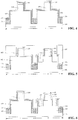
- FIG. 1 shows a schematic cross-section view of a conventional Fin-FET device.
- the Fin-FET device includes two complementary metal-oxide-semiconductor (CMOS) transistors.
- CMOS complementary metal-oxide-semiconductor
- the fabrication process for the Fin-FET device includes the following steps.
- a substrate 10 is provided and two fin structures 11 are formed on the substrate 10. Specifically, the fin structures 11 protrude from the substrate 10. Moreover, an isolation structure 12 is formed on the substrate and the isolation structure 12 covers a portion of the top surfaces of the fin structures 11.
- the substrate 10 includes a P-type metal-oxide-semiconductor (PMOS) region and an N-type metal oxide-semiconductor (NMOS) region, and each of the PMOS region and the NMOS region includes one fin structure 11.
- PMOS P-type metal-oxide-semiconductor
- NMOS N-type metal oxide-semiconductor
- first gate structure 21 is formed on the isolation structure 12 across the fin structure 11 in the PMOS region and a second gate structure 22 is formed on the isolation structure 12 across the fin structure 11 in the NMOS region.
- a sidewall spacer 13 is then formed on each sidewall surface of the first gate structure 21 and the second gate structure 22.
- first doped source/drain regions 31 are formed in the fin structure 11 in the PMOS region on the two opposite sides of the first gate structure 21 and second doped source/drain regions 32 are formed in the fin structure 11 in the NMOS region on the two opposite sides of the second gate structure 22.
- a dielectric layer 14 is formed on the first doped source/drain regions 31, the second doped source/drain regions 32, the isolation structure 12, the first gate structure 21, and the second gate structure 22.
- the top surface of the dielectric layer 14 is higher than the top surface of the first gate structure 21.
- each via exposes a portion of the surface of a corresponding first doped source/drain region 31 or a corresponding second doped source/drain region 32.
- a metal contact layer 16 is formed on the exposed portion of the surfaces of the first doped source/drain regions 31 and the second doped source/drain regions 32 on the bottom of the vias. Then, a conductive plug 15 is formed on the metal contact layer 16 to fill up each of the four vias.
- the formed vias in order to avoid exposing the first gate structure 21 or the second gate structure 22 during the etching process to form the vias, the formed vias usually has a relatively narrow width. Thus, a portion of the surfaces of the first doped source/drain regions 31 and a portion of the surfaces of the second doped source/drain regions 32 are exposed on the bottom of the vias. As such, the metal contact layer 16 may only be formed on a portion of the surfaces of the first doped source/drain regions 31 and a portion of the surfaces of the second doped source/drain regions 32. Therefore, the effect of the metal contact layer 16 to reduce the contact resistance of the Fin-FET device may be limited.
- the present invention provides a method for fabricating Fin-FET devices.
- Figure 17 shows a flowchart of an exemplary method for fabricating a Fin-FET device consistent with various disclosed embodiments in the present invention.
- Figures 2-16 show schematic cross-section views of semiconductor structures at certain stages of the exemplary method for fabricating the Fin-FET device.
- a plurality of fin structures may be formed on a substrate and an isolation structure may be formed on the substrate to cover a portion of the sidewall surfaces of each fin structure (S1 101).
- Figure 2 shows a schematic cross-section view of a corresponding semiconductor structure.
- a plurality of fin structures 102 are formed on a substrate 101.
- An isolation structure 103 may also be formed on the substrate 101 to cover a portion of the sidewall surfaces of each fin structure 102.
- the Fin-FET device to be formed is described to be a CMOS device, and the substrate 101 may include an NMOS region I and a PMOS region.
- the NMOS region I may provide a process platform for forming an NMOS transistor and the PMOS region II may provide a process platform for forming a PMOS transistor.
- the substrate may only include PMOS region(s) or may only include NMOS region(s). Accordingly, the Fin-FET device to be formed may only include PMOS transistor(s) or may only include NMOS transistor(s).
- the substrate 101 may be made of silicon, germanium, SiGe, SiC, GaAs, InAs, or any other appropriate semiconductor material.
- the substrate 101 may also be made of silicon on insulator (SOI), germanium on insulator (GOI), or any other semiconductor structure.
- the plurality of fin structures 102 may be made of silicon, germanium, SiGe, SiC, GaAs, InAs, or any other appropriate semiconductor material.
- the substrate 101 is made of silicon and the plurality of fin structures 102 are also made of silicon.
- the substrate 101 and the plurality of fin structures 102 may be formed by a process including the following steps. First, an initial substrate may be provided. A patterned layer may then be formed on the surface of the initial substrate. Further, the initial substrate may be etched using the patterned layer as an etch mask to form the substrate 101 and the plurality of fin structures 102 protruding from the surface of the substrate 101.
- the isolation structure 103 formed on the substrate 101 may be used to electrically isolate neighboring fin structures 102.
- the isolation structure 103 may be made of an insulating material such as SiO x , SiN x , SiON, SiCON, etc. In one embodiment, the isolation structure 103 is made of SiO x .
- a plurality of dummy gate structures may be formed on the isolation structure across the plurality of fin structures to cover a portion of the top and the sidewall surfaces of each fin structure (S1102).
- a plurality of dummy gate structures may be formed on the isolation structure 103 across the plurality of fin structures 102.
- the plurality of dummy gate structures may cover a portion of the top and the sidewall surfaces of each fin structure 102.
- the substrate 101 may include an NMOS region I used to form a plurality of NMOS transistors and a PMOS region II used to form a plurality of PMOS transistors.
- the plurality of dummy gate structures may be formed by a process including forming first dummy gate structures 110 on the isolation structure 103 in the NMOS region I and across the fin structures 102 in the NMOS region I and forming second dummy gate structures 120 on the isolation structure 103 in the PMOS region II and across the fin structures 102 in the PMOS region II.
- first dummy gate structures and a plurality of second dummy gate structures may be formed on the substrate 101, only one first dummy gate structure 110 in the NMOS region I and one second dummy gate structure 120 in the PMOS region II are shown in Figure 2 .
- the formed dummy gate structures include both the plurality of first dummy gate structures 110 and the plurality of second dummy gate structures 120.
- the first dummy gate structure 110 may be removed and a first gate structure may then be formed at the position of the first dummy gate structure 110.
- the second dummy gate structure 120 may be removed and a second gate structure may then be formed at the position of the second dummy gate structure 120.
- the first dummy gate structure 110 may have a single-layer structure or a multiple-layer structure.
- the first dummy gate structure 110 may include a dummy gate electrode layer, or may include a dummy oxide layer and a dummy gate electrode formed on the dummy oxide layer.
- the dummy gate electrode may be made of polycrystalline silicon or amorphous carbon, and the dummy oxide layer may be made of SiO x or SiON.
- the first dummy gate structures 110 and the second dummy gate structures 120 may be formed by a process including the following steps.
- a dummy gate film may be formed on the surface of the isolation structure 103.
- the dummy gate film may be formed across the plurality of fin structures 102 and covering the top and the sidewall surfaces of the plurality of fin structures 102.
- a hard mask layer 104 may be formed on the surface of the dummy gate film.
- the hard mask layer 104 may be made of SiN x , SiON, SiC, BN, etc.
- the hard mask layer 104 may define the pattern of the subsequently-formed first dummy gate structures 110 and the pattern of the subsequently-formed second dummy gate structures 120.
- the plurality of first dummy gate structures 110 may be formed on the portion of the isolation structure 103 in the NMOS region I and the plurality of second dummy gate structures 120 may be formed on the portion of the isolation structure 103 in the PMOS region II.
- the portion of the hard mask layer 104 formed on the top surfaces of the first dummy gate structures 110 and the second dummy gate structures 120 may be retained after the patterning process.
- the remaining portion of the hard mask layer 104 may provide protection for the top of the first dummy gate structures 110 and the top of the second dummy gate structures 120 during subsequent fabrication processes, preventing the top of the first dummy gate structures 110 and/or the top of the second dummy gate structures 120 from declining. Therefore, the top of the subsequently-formed first gate structures and the top of the subsequently-formed second gate structures may be ensured to meet desired process requirements.
- an offset spacer may be formed on each sidewall surface of the dummy gate structures (S1103).
- Figure 3 shows a schematic cross-section view of a corresponding semiconductor structure.
- an offset spacer 105 may be formed on each sidewall surface of the dummy gate structures. After forming a plurality of first gate structures and a plurality of second gate structures in subsequent processes, the offset spacer 105 may be situated on the sidewall surfaces of the first gate structures and the second gate structures.
- the offset spacer 105 may be formed on the sidewall surfaces of the first dummy gate structures 110 and the second dummy gate structures 120.
- a portion of the fin structures 102 in the NMOS region I on the two opposite sides of each first dummy gate structure 110 as well as a portion of the fin structures 102 in the PMOS region II on the two opposite sides of each second dummy gate structure 120 may be removed by etching.
- the offset spacer 105 may also be formed on the sidewall surfaces of the fin structures 102, the top surfaces of the dummy gate structures, and the top surface of the isolation structure 103. That is, the offset spacers 105 may be formed on the top and the sidewall surfaces of the fin structures 102, the surface of the isolation structure 103, the top and the sidewall surfaces of the first dummy gate structures 110, as well as the top and the sidewall surfaces of the second dummy gate structures 120.
- the offset spacer 105 may be formed through chemical vapor deposition (CVD), physical vapor deposition (PVD), or atomic layer deposition (ALD).
- the offset spacer 105 may be made of SiO x , SiN x , or SiON.
- the offset spacer 105 is formed by CVD and made of SiN x . Moreover, the thickness of the formed offset spacer 105 may be in a range of approximately 2 nm to 3 nm.
- the offset spacer may only cover the sidewall surfaces of the first dummy gate structures and the second dummy gate structures.
- the process to form the offset spacer may include the following steps. First, an offset spacing film may be formed to cover the top and the sidewall surfaces of the dummy gate structures and the surface of the isolation structure. Then, a maskless back etching process may be performed on the offset spacing film to remove the portion of the offset spacing film formed on the top surfaces of the dummy gate structures and on the surface of the isolation structure. As such, the offset spacer covering the sidewall surface of the first dummy gate structure and the sidewall surface of the second dummy gate structure may be formed. In addition, the formed offset spacer may also cover the sidewall surfaces of the fin structures.
- the fabrication process may further include performing a first light doping process on the portion of the fin structure 102 on the two opposite sides of each first dummy gate structure 110 in the NMOS region.
- a first lightly-doped source/drain region (not shown) may be formed in the fin structure 102 on each side of the offset spacer 105 in the NMOS region.
- the type of the doping ions used in the first light doping process may be N-type ions.
- the fabrication process may also include performing a second light doping process on the portion of the fin structure 102 on the two opposite sides of each second dummy gate structure 120 in the PMOS region.
- a second lightly-doped source/drain region may be formed in the fin structure 102 on each side of the offset spacer 105 in the PMOS region.
- the type of the doping ions used in the second light doping process may be P-type ions.
- an annealing process may be performed on the plurality of fin structures 102.
- the first lightly-doped source/drain region may be used as a lightly-doped drain (LDD) structure of the NMOS region I while the second lightly-doped source/drain region may be used as a LDD of the PMOS region II.
- LDD lightly-doped drain
- the offset spacer when forming LDD structure in the Fin-FET device is not required, forming the offset spacer may not be necessary. Accordingly, the sidewall spacer subsequently formed on the sidewall surfaces of the gate structures may have a single-layer structure.
- a mask layer may be formed on the isolation structure, the offset spacer, as well as the top surfaces of the dummy gate structures.
- Figure 4 shows a schematic cross-section view of a corresponding semiconductor structure.
- a mask layer 106 may be formed on the isolation structure, the offset spacer, and the top surfaces of the dummy gate structures.
- the mask layer 106 may cover the surface of the offset spacer 105.
- the mask layer may cover the surface of the fin structures, the surface of isolation structure, the top surfaces of the dummy gate structures, as well as the surface of the offset spacer.
- the use of the mask layer 106 may include several aspects. First, during a subsequent process to etch a portion of the fin structure 102 formed in the NMOS region I, the mask layer 106 may be used as an etch mask to ensure a certain distance between a subsequently-formed first opening and the previously-formed first lightly-doped source/drain region, and thus avoid complete removal of the first lightly-doped source/drain region. Further, in a subsequent process, the portion of the mask layer 106 formed in the NMOS region I may be etched to form a mask sidewall on each sidewall surface of the fin structure 102 in the NMOS region I.
- the mask sidewalls may further be used as a mask to form first doped source/drain regions on the two opposite sides of the fin structure 102 in the NMOS region I.
- the mask layer 106 may be used as an etch mask to ensure a certain distance between a subsequently-formed second opening and the previously-formed second lightly-doped source/drain region, and thus avoid complete removal of the second lightly-doped source/drain region.
- the portion of the mask layer 106 formed in the PMOS region II may be etched to form a mask sidewall on each sidewall surface of the fin structure 102 in the PMOS region II.
- the mask sidewalls may further be used as a mask to form second doped source/drain regions on the two opposite sides of the fin structure 102 in the PMOS region II.
- the portion of the mask layer 106 formed on the sidewall surface as well as a portion of the top surface of each fin structure 102 may serve as a silicide block layer during a subsequent annealing process to prevent a subsequently-formed metal layer from reacting with the portion of the fin structure 102 not supposed to have a metal contact layer formed on.
- the mask layer 106 and the fin structures 102 may be made of different materials.
- the mask layer 106 may be made of SiO x , SiN x , SiON, etc. Because the mask layer 106 may be used as the etch mask in a subsequent process to etch the fin structures 102, in order to ensure the subsequently-formed mask sidewalls provide sufficient protection for the first gate structures and the second gate structures, the mask layer 106 may be made of a material including SiN x due to the advantage of high density that SiN x demonstrates.
- the mask layer 106 may have a single SiN x layer structure or have a multi-layer structure including at least one SiN x layer. For example, the mask layer 106 may have an oxide-nitride-oxide (ONO) structure.
- the mask layer 106 is made of SiN x , and the thickness of the mask layer 106 may be in a range of approximately 3 nm to 6 nm.
- two first openings may be formed in each fin structure in the PMOS region by removing a portion of the fin structure on each side of the dummy gate structure in the PMOS region (S1104).
- Figure 5 shows a schematic cross-section view of a corresponding semiconductor structure.
- two first openings 201 may be formed in the fin structure 102 in the PMOS region II by removing a portion of the fin structure 102 on each side of the second dummy gate structure 120 in the PMOS region.
- the portion of the mask layer 106 formed in the PMOS region II may be etched to form a mask sidewall 116 to cover a sidewall surface of the corresponding offset spacer 105 in the PMOS region II.
- the thickness of the mask sidewall 116 may be in a range of approximately 3 nm to 6 nm.
- the mask layer 106 formed on a portion of the top and the sidewall surfaces of the fin structure 102 in the PMOS region II may be retained.
- the remaining portion of the mask layer 106 may prevent undesired epitaxial growth during a subsequent process to form a first stress layer.
- the remaining portion of the mask layer 106 formed on the portion of the top and the sidewall surfaces of the fin structures 102 in the PMOS region II may serve as a silicide block layer.
- the first openings 201 may be formed by a process including the following steps. First, a first patterned layer 107 may be formed to cover the NMOS region I. The first patterned layer 107 may also cover a portion of the mask layer 106 formed in the PMOS region II and may expose a portion of the surface of the mask layer 106 formed on the two opposite sides of the second dummy gate structure 120. Then, a mask sidewall 116 may be formed on each side of the second dummy gate structure 120 by etching the mask layer 106 formed on the two sides of the second dummy gate structure 120 using the first patterned layer 107 as an etch mask. Further, a portion of the fin structure 102 formed in the PMOS region II may be removed by etching using the mask sidewall 116 as an etch mask to form the first openings 201.
- the portion of the fin structures 102 in the PMOS region II may be removed by an anisotropic etching process.
- the anisotropic etching process may be a reactive ion etching process.
- the process parameters adapted in the reactive ion etching process may include a reaction gas including CF 4 , SF 6 , and Ar, a flow rate of CF 4 in a range of approximately 50 sccm to 100 sccm, a flow rate of SF 6 in a range of approximately 10 sccm to 100sccm, a flow rate of Ar in a range of approximately 100 seem to 300 sccm, a source power in a range of 500 W to 1000 W, an offset power in a range of approximately 50 W to 250 W, a chamber pressure in a range of approximately 50 mTorr to 200 mTorr, and a chamber temperature in a range of approximately 20 °C to 90 °C.
- the depth of each first opening 201 may be
- the first patterned layer 107 may be removed.
- the first patterned layer 107 may be made of photoresist.
- the first patterned layer 107 may be removed by a wet photoresist-removal process or by an ashing process.
- a second doped source/drain region may be formed in the fin structure on each side of the dummy gate structure in the PMOS region (S1105).
- Figure 6 shows a schematic cross-section view of a corresponding semiconductor structure.
- a second doped source/drain region 211 may be formed in the fin structure 102 in the PMOS region II on each side of the second dummy gate structure 120.
- the second doped source/drain regions 211 may be fabricated by a process including the following steps.
- a first stress layer (not shown) may be formed to fill up each first opening 201 (referring to Figure 5 ).
- an in-situ ion implantation process may be simultaneously performed to form a second source/drain doped region 211 in the fin structure 102 in the PMOS region II next to each mask sidewall 116.
- an ion implantation process may then be performed on the first stress layer to form a second source/drain doped region 211 in the fin structure 102 in the PMOS region II next to each mask sidewall 116.
- the first stress layer may be made of SiGe, SiB, SiGeB, or any other appropriate material.
- the first stress layer may provide stress to the channel region in the PMOS region II and thus may improve the carrier mobility in the PMOS region II.
- the first stress layer may be formed by a selective epitaxial process.
- the sidewall spacer on each side of the second dummy gate structure 120 may include an offset spacer 105 and a mask sidewall 116 formed on the side surface of the offset spacer 105. In other embodiments, the sidewall spacer on each side of the second dummy gate structure 120 may only include a mask sidewall.
- an oxygen treatment process may be performed on the top surface of the first stress layer so that an oxide layer may be formed on the surface of the first stress layer.
- two second openings may be formed in each fin structure in the NMOS region by removing a portion of the fin structure on each side of the dummy gate structure in the NMOS region (S1106).
- Figure 7 shows a schematic cross-section view of a corresponding semiconductor structure.
- two second openings 202 may be formed in the fin structure 102 in the NMOS region I by removing a portion of the fin structure 102 on each side of the first dummy gate structure 110 in the NMOS region.
- the portion of the mask layer 106 formed in the NMOS region I may be etched to form a mask sidewall 116 to cover a sidewall surface of the corresponding offset spacer 105 in the NMOS region I.
- the thickness of the mask sidewall 116 may be in a range of approximately 3 nm to 6 nm.
- the mask layer 106 formed on a portion of the top and the sidewall surfaces of the fin structure 102 in the NMOS region I may be retained.
- the remaining portion of the mask layer 106 may prevent undesired epitaxial growth during a subsequent process to form a second stress layer.
- the remaining portion of the mask layer 106 formed on the portion of the top and the sidewall surfaces of the fin structure 102 in the NMOS region I may serve as a silicide block layer.
- the second openings 202 may be formed by a process including the following steps. First, a second patterned layer 108 may be formed to cover the PMOS region II. The second patterned layer 108 may also cover a portion of the mask layer 106 formed in the NMOS region I and may expose a portion of the surface of the mask layer 106 formed on the two opposite sides of the first dummy gate structure 110. Then, a mask sidewall 116 may be formed by on each side of the first dummy gate structure 110 by etching the mask layer 106 formed on the two sides of the first dummy gate structure 110 using the second patterned layer 108 as an etch mask. Further, a portion of the fin structure 102 formed in the NMOS region I may be removed by etching using the mask sidewall 116 as an etch mask to form the second openings 202.
- the portion of the fin structures 102 in the NMOS region I may be removed by an anisotropic etching process.
- the anisotropic etching process may be a reactive ion etching process.
- the process parameters adapted in the reactive ion etching process may include a reaction gas including CF 4 , SF 6 , and Ar, a flow rate of CF 4 in a range of approximately 50 sccm to 100 sccm, a flow rate of SF 6 in a range of approximately 10 sccm to 100sccm, a flow rate of Ar in a range of approximately 100 sccm to 300 sccm, a source power in a range of 500 W to 1000 W, an offset power in a range of approximately 50 W to 250 W, a chamber pressure in a range of approximately 50 mTorr to 200 mTorr, and a chamber temperature in a range of approximately 20 °C to 90 °C.
- the second patterned layer 108 may be removed.
- the second patterned layer 108 may be made of photoresist.
- the second patterned layer 108 may be removed by a wet photoresist-removal process or by an ashing process.
- first doped source/drain regions may be formed in the fin structure on the two opposite sides of the dummy gate structure in the NMOS region (S1107).
- Figure 8 shows a schematic cross-section view of a corresponding semiconductor structure.
- a first doped source/drain region 212 may be formed in the fin structure 102 in the NMOS region I on each side of the first dummy gate structure 110.
- the first doped source/drain regions 212 may be fabricated by a process including the following steps.
- a second stress layer (not shown) may be formed to fill up the second openings 202 (referring to Figure 7 ).
- an in-situ ion implantation process may be simultaneously performed to form a first source/drain doped region 212 in the fin structure 102 in the NMOS region I next to each mask sidewall 116.
- an ion implantation process may then be performed on the second stress layer to form a first source/drain doped region 212 in the fin structure 102 in the NMOS region I next to each mask sidewall 116.
- the second stress layer may be made of SiCP, SiC, SiP, or any other appropriate material.
- the second stress layer may provide stress to the channel region in the NMOS region I, and thus may improve the carrier mobility in the NMOS region I.
- the second stress layer may be formed by a selective epitaxial process.
- the sidewall spacer on each side of the first dummy gate structure 110 may include an offset spacer 105 and a mask sidewall 116 formed on the side surface of the offset spacer 105. In other embodiments, the sidewall spacer on each side of the first dummy gate structure 110 may only include a mask sidewall.
- an oxygen treatment process may be performed on the top surface of the second stress layer so that an oxide layer may be formed on the surface of the second stress layer.
- the top surfaces of the first stress layer and the second stress layer may be oxidized through a same oxygen treatment process. In other embodiments, the top surfaces of the first stress layer and the second stress layer may be oxidized through different oxygen treatment processes.
- a dummy dielectric layer may be formed in the first doped source/drain regions and the second doped source/drain regions and also on the sidewall surfaces of the dummy gate structures (S1108).
- Figure 9 shows a schematic cross-section view of a corresponding semiconductor structure.
- a dummy dielectric layer 301 may be formed in the first doped source/drain regions 211 and the second doped source/drain regions 212 and also on the sidewall surfaces of the dummy gate structures.
- the dummy dielectric layer 301 may expose the top surfaces of the dummy gate structures.
- the dummy dielectric layer 301 may be formed on the first doped source/drain regions 211, the second doped source/drain regions 212, the mask sidewalls 116, the mask layer 106, the first dummy gate structures 110, and the second dummy gate structures 120.
- the dummy dielectric layer 301 may be made of a material different from the materials used to form the fin structures 102, the first dummy gate structures 110, the second dummy gate structures 120, the first stress layer, and the second stress layer. Moreover, in one embodiment, the dummy dielectric layer 301 may be made of SiO x .
- the top surface of the dummy dielectric layer 301 may be leveled with the top surfaces of the first dummy gate structures 110 and the second dummy gate structures 120.
- the dummy dielectric layer 301 may be formed by a process including the following steps. First, a dummy dielectric film may be formed on the first stress layer, the second stress layer, the mask sidewalls 116, the mask layer 106, and the hard mask layer 104 (referring to Figure 8 ). The top surface of the dummy dielectric film may be higher than the top surfaces of the first dummy gate structures 110 and the second dummy gate structures 120.
- a planarization process may be performed on the dummy dielectric film to remove the portion of the dummy dielectric film formed above the top surfaces of the first dummy gate structures 110 and the second dummy gate structures 120.
- the dummy dielectric layer 301 with a top surface leveled with the top surfaces of the first dummy gate structures 110 and the second dummy gate structures 120 may be formed.
- each dummy gate structure may be removed to form a trench in the dummy dielectric layer, and then a gate structure may be formed in each trench (S1109).
- Figure 10 shows a schematic cross-section view of a corresponding semiconductor structure.
- each first dummy gate structure 110 (referring to Figure 9 ) and each second dummy gate structure 120 (referring to Figure 9 ) may be removed to form a first trench and a second trench, respectively in the dummy dielectric layer 301. Then, a high-k dielectric layer may be formed on the sidewall and the bottom surfaces of the first trench and the second trench. Further, a gate electrode may be formed on the high-k dielectric layer in each of the first trench and the second trench.
- the first dummy gate structure 110 (referring to Figure 9 ) may be removed by etching to form the first trench in the dummy dielectric layer 301 in the PMOS region I.
- the second dummy gate structure 120 (referring to Figure 9 ) may also be removed by etching to form the second trench in the dummy dielectric layer in the NMOS region II.
- the high-k dielectric layer and the gate electrode formed in the first trench may together form a first gate structure 210.
- the first gate structure 210 may be situated on the isolation structure 103 in the PMOS region I.
- the first gate structure 210 may be formed across the fin structure 102 in the PMOS region I and may cover a portion of the top and the sidewall surfaces of the fin structure 102 in the PMOS region I.
- the high-k dielectric layer and the gate electrode formed in the second trench may together form a second gate structure 220.
- the second gate structure 220 may be situated on the isolation structure 103 in the NMOS region II.
- the second gate structure 220 may be formed across the fin structure 102 in the NMOS region II and may cover a portion of the top and the sidewall surfaces of the fin structure 102 in the NMOS region II.
- each side surface of the first gate structure 210 may be covered by a sidewall spacer and the sidewall may include an offset spacer 105 and a mask sidewall 116.
- each side surface of the second gate structure 220 may be covered by a sidewall spacer and the sidewall may also include an offset spacer 105 and a mask sidewall 116.
- the high-k dielectric layer is made of a high-k dielectric material.
- the high-k dielectric material may refer to a material with a relative dielectric constant greater than the relative dielectric constant of SiO x .
- the high-k dielectric layer may be made of one or more of HfO 2 , HfSiO, HfSiON, HfTaO, HfTiO, HfZrO, ZrO 2 , Al 2 O 3 , etc.
- the gate electrode layer may be made of a material including Cu, Al, W, etc.
- the fabrication process may also include performing a repair annealing process on the high-k dielectric layer.
- the anneal temperature used in the repair annealing process may need to be higher than the anneal temperature used in a subsequently-performed reaction annealing process.
- the gate electrode is directly formed on the top of the corresponding high-k dielectric layer.
- a work function layer may be formed between the high-k dielectric layer and the gate electrode. The work function layer may be used to adjust the threshold voltage of the subsequently-formed NMOS transistor or PMOS transistor.
- FIG. 11 shows a schematic cross-section view of a corresponding semiconductor structure.
- each gate electrode may be removed. Further, a cap layer 302 may be formed on the remaining portion of gate electrode.
- a metal layer may be formed on the top surfaces of the first gate structures 210 and the second gate structures 220. Then, a reaction annealing process may be performed to remove the unreacted portion of the metal layer. Therefore, in order to avoid damages to the first gate structures 210 and the second gate structures 220 due to the removal of the unreacted metal layer, a cap layer 302 may be formed between the top of the first gate structure 210 and the metal layer and also between the top of the second gate structure 220 and the metal layer.
- the cap layers 302 may be formed by a process including the following steps. First, a portion of each gate electrode may be removed through a maskless etching process. Further, a cap film may be formed on the dummy dielectric layer 301 and the remaining portion of each gate electrode. The top surface of the cap film may be higher than the top surface of the dummy dielectric layer 301. The portion of the cap film formed above the top surface of the dummy dielectric layer 301 may be removed by polishing to form the cap layer 302.
- the cap layer 302 may be made of a material different from the material of the dummy dielectric layer 301. In addition, the material used to form the cap layer 302 may not react with the subsequently-formed metal layer. Therefore, in one embodiment, the cap layer 302 is made of SiN x . In other embodiments, the cap layer 302 may also be made of BN.
- the thickness of the cap layer 302 may not be too small or too large. When the thickness of the cap layer 302 is too small, the cap layer 302 may be easily removed during a subsequently-performed process to remove the dummy dielectric layer 301. However, when the thickness of the cap layer 302 is too large, an excessive amount of the gate electrode may be removed before forming the cap layer, and thus the electrical performance of the first gate structures 210 and the second gate structures 220 may be affected. In one embodiment, the thickness of the cap layer may be in a range of approximately 5 ⁇ to 35 ⁇ .
- the dummy dielectric layer may be removed to expose the surface of each first doped source/drain region and each second doped source/drain region (S1111).
- Figure 12 shows a schematic cross-section view of a corresponding semiconductor structure.
- the dummy dielectric layer 301 (referring to Figure 11 ) may be removed to expose the surfaces of the first doped source/drain regions 211 and the second doped source/drain regions 212.
- the dummy dielectric layer 301 may be removed by a wet etching process. Specifically, for a dummy dielectric layer 301 made of SiO x , a HF solution may be used as the etch solution to remove the dummy dielectric layer 301.
- a metal layer may be formed on the doped source/drain regions, the sidewall spacers, and the gate structures (S1112).
- Figure 13 shows a schematic cross-section view of a corresponding semiconductor structure.
- a metal layer 303 may be formed on the first doped source/drain regions 212, the second doped source/drain regions 211, and the sidewall spacers as well as the top surfaces of the first gate structures 210 and the second gate structures 220.
- the metal layer 303 may also be formed on the mask layer 106.
- the mask layer 106 may serve as a silicide block layer during a subsequently-performed reaction annealing process.
- the portion of the metal layer 303 formed on the top of each gate structure may cover the corresponding cap layer 302.
- the metal layer 303 may be made of a mono-metal or an alloy of Ni, W, Ti, Ta, Pt, Co, etc.
- the metal layer 303 may be formed by physical vapor deposition (PVD), metal sputtering, or atomic layer deposition (ALD).
- the metal layer 303 may be used to provide metal atoms for forming a metal contact layer, e.g., a metal silicide layer, in a subsequent process.
- the material of the metal layer 303 may react with the material of the first doped source/drain regions and the second doped source/drain regions. Further, when the metal layer 303 is made of Ni, the consumed portion of the material of the first doped source/drain regions and the second doped source/drain regions may be small during a subsequently performed chemical reaction. Moreover, the line width of the formed metal contact layer may be small, and thus the process cost may be relatively low.
- the metal layer 303 may be made of Ni and may have a thickness in a range of approximately 50 ⁇ to 200 ⁇ .
- a protective layer may be formed on the surface of the meal layer 303.
- the protective layer may separate the metal layer 303 from O 2 in the environment.
- the protective layer may be made of Ti, Ta, TiN, TaN, or any other appropriate material.
- a reaction annealing process may be performed to convert the portion of the metal layer formed on the doped source/drain regions into a metal contact layer through chemical reaction, and the unreacted portion of the metal layer may be removed after the reaction annealing process (S1113).
- Figure 14 shows a schematic cross-section view of a corresponding semiconductor structure.
- a reaction annealing process may be performed on the metal layer 303 (referring to Figure 13 ).
- the portion of the metal layer 303 formed on the first doped source/drain regions and the second doped source/drain regions may be converted to a metal contact layer 305 through chemical reaction.
- the unreacted portion of the metal layer 303 may be removed. That is, the portion of the metal layer 303 formed on the top surfaces of the sidewall spacers, the first gate structures 210, the second gate structures 220, and the mask layer 106 may be removed.
- the metal contact layer 305 may be used to reduce the contact resistance in the formed Fin-FET devices.
- the metal layer 303 may be made of Ni and the fin structures 102 may be made of Si. Accordingly, the metal contact layer 305 may be made of SiNi x .
- the metal layer may be made of Ti, the fin structures may be made of Si, and accordingly, the metal contact layer may be made of SiTi x .
- the metal layer 303 may cover the entire surface of each first doped source/drain region 212 as well as the entire surface of each second doped source/drain region 211. Therefore, after the reaction annealing process, the formed metal contact layer 305 may cover the entire surface of each first doped source/drain region 212 and the entire surface of each second doped source/drain region 211.
- the disclosed fabrication methods ensure the metal contact layer 305 cover the entire surface of each first doped source/drain region and the entire surface of each second doped source/drain region, and thus, after forming the metal contact layer 305, the contact resistance in the formed Fin-FET devices may be smaller so that the operation speed of the formed Fin-FET devices may be improved.
- the material of the metal layer 303 may react with the material of the first doped source/drain regions and the second doped source/drain regions.
- the first doped source/drain regions and the second doped source/drain regions may include a large number of silicon atoms, and accordingly, the chemical reaction may be silicide reaction.
- the metal layer 303 may not react with the cap layer 302.
- the mask layer 106 formed on the sidewall surfaces of the fin structures 102 as well as a portion of the top surfaces of the fin structures 102 may serve as a silicide block layer to prevent chemical reaction between the fin structures 102 and the metal layer 303.
- the metal contact layer may not be formed on the undesired region of the fin structures 102.
- laser annealing, spike annealing, or millisecond annealing may be performed during the reaction annealing process.
- laser annealing is performed during the reaction annealing process.
- the anneal temperature used in the reaction annealing process may not be too low or too high. When the anneal temperature is too low during the reaction annealing process, the silicidation degree of the formed metal contact layer 305 may be low, and thus the resistivity of the metal contact layer 305 may be high. However, when the anneal temperature in the reaction annealing process is too high, the properties of the metal contact layer 305 may be changed at such a high temperature, and thus the quality of the formed metal contact layer 305 may be undesired.
- the reaction annealing process is a laser annealing process and the anneal temperature is in a range of approximately 800 °C to 880 °C, such as 800 °C, 850 °C, and 880 °C.
- the metal contact layer 305 may be formed after forming the first gate structures 210 and the second gate structures 220. As such, undesired effects on the metal contact layer 305 due to the fabrication process for the first gate structures 210 and the second gate structures 220 may be avoided.
- a repair annealing process may be performed on the high-k dielectric layers.
- the anneal temperature used in the repair annealing process may be higher than the anneal temperature used in the reaction annealing process. Therefore, the metal contact layer 305 may not be formed before forming the high-k dielectric layers; otherwise, the metal contact layer 305 may be damaged during the repair annealing process, resulting in degraded properties of the metal contact layer 305.
- the unreacted portion of the metal layer 303 may be removed.
- the process to remove the unreacted portion of the metal layer 303 may include removing the portion of the metal layer 303 covering the cap layers 302 and removing the portion of the metal layer 303 formed on the mask layer 106.
- the unreacted portion of the metal layer 303 may be removed by a wet etching process.
- the wet etching process may use a mixture of sulfuric acid and hydrogen peroxide as an etch solution.
- the protective layer 304 may be removed prior to removing the unreacted portion of the metal layer 303.
- the protective layer 304 may be removed by a wet etching process using a mixture of sulfuric acid and hydrogen peroxide as an etch solution.
- a dielectric layer with a top surface higher than the top surfaces of the gate structures may be formed on the metal contact layer, the sidewall spacers, and the gate structures (S1114).
- Figure 15 shows a schematic cross-section view of a corresponding semiconductor structure.
- a dielectric layer may be formed on the metal contact layer 305, the offset spacers 105, the mask sidewalls 116, the first gate structures 210, and the second gate structures 220.
- the top surface of the dielectric layer may be higher than the top surfaces of the first gate structures 210 and the second gate structures 220.
- the dielectric layer may include a first dielectric layer 306 and a second dielectric layer 307 formed on the first dielectric layer 306 with the density of the first dielectric layer 306 greater than the density of the second dielectric layer.
- the process to form the dielectric layer may include forming the first dielectric layer 306 through a high-density plasma deposition process with the top surface of the first dielectric layer 306 leveled with the top surfaces of the first gate structures 210 and the second gate structures 220, and then forming a second dielectric layer 307 on the first dielectric layer 306 through a plasma-enhanced tetraethyl orthosilication (PETEOS) process.
- PETEOS plasma-enhanced tetraethyl orthosilication
- a cap layer 302 may be formed on the top surfaces of the first gate structures 210 and the second gate structures 220; accordingly, the top surface of the first dielectric layer 306 may be leveled with the top surface of the cap layer 302.
- the fabrication process may further include a chemical mechanical polishing (CMP) process to remove the portion of the first dielectric layer 306 formed above the top surfaces of the first gate structures 210 and the second gate structures 220.
- CMP chemical mechanical polishing
- a via may be formed through the dielectric layer to expose a portion of the metal contact layer 305 formed on each doped source/drain region, and then a conductive plug may be formed to fill the via (S1115).
- Figure 16 shows a schematic cross-section view of a corresponding semiconductor structure.
- a via may be formed through the first dielectric layer 306 and the second dielectric layer 307 to expose a portion of the surface of the corresponding metal contact layer 305. Further, a conductive plug 308 may be formed to fill up each via. The conductive plug 308 may be electrical connected to the corresponding first doped source/drain region or second doped source/drain region through the metal contact layer 305.
- each via may expose a portion of the surface of the metal contact layer 305 such that the subsequently-formed conductive plug 308 may not be electrically connected to the first gate structures 210 or the second gate structures 220.
- the process to form the vias in the dielectric layer may include the following steps. First, a patterned photoresist layer may be formed on the top of the dielectric layer. Then, the vias may be formed by etching the second dielectric layer 307 and the first dielectric layer 306 using the patterned photoresist layer as an etch mask until a portion of the surface of the metal contact layer 305 is exposed. Finally, the patterned photoresist layer may be removed.
- the conductive plug 308 may be made of a material including Cu, Al, W, and any other appropriate material. In one embodiment, the conductive plug 308 is made of W.
- the process to form the conductive plugs 308 may include the following steps. First, a conductive film may be formed to fill up the vias. The conductive film may also be formed on the top surface of metal contact layer 305. Then, a planarization process may be performed on the conductive film to remove the portion of the conductive film formed on the top of the dielectric layer and thus form the conductive plugs 308. Moreover, the formed conductive plugs 308 may fill up the vias.
- the formed metal contact layer 305 may be situated on the entire surface of each first doped source/drain region 212 and also on the entire surface of the second doped source/drain region 211. Further, only a portion of the formed metal contact layer 305 may be in contact with the corresponding conductive plug 308. That is, the surface area of each metal contact layer 305 may be larger than the bottom surface of the corresponding conductive plug 308. Therefore, the contact resistance in the Fin-FET devices formed by the disclosed fabrication method may be small, leading to a higher operation speed of the formed Fin-FET devices.
- the gate structures including the first gate structures 210 and the second gate structures 220, may be metal gate structures.
- the fabrication process is described to form doped source/drain regions before forming the gate structures.
- the gate structures when the gate structures are metal gate structures, the gate structures may also be formed before forming the doped source/drain regions.
- a cap layer may be formed on the gate structures prior to forming the metal layer. Further, during the process to remove the unreacted portion of the metal layer, the portion of the metal layer formed on the cap layer may also be removed.
- the process to form the Fin-FET devices may include providing a substrate and forming a plurality of fin structures on the substrate.
- the fin structures may bulge from the surface of the substrate.
- an isolation structure covering a portion of the sidewall surfaces of the fin structures may also be formed on the substrate, and the top surface of the isolation structure may be lower than the top surfaces of the fin structures.
- a plurality of gate structures may be formed on the isolation structure across the fin structures.
- the gate structures may be metal gate structures and the gate structures may cover a portion of the top and sidewall surfaces of each fin structure. Further, each sidewall of the gate structures may be covered by a sidewall spacer.
- two doped source/drain regions may be formed in the fin structure on the two opposite sides of each gate structure, and a cap layer may be formed on the top of the gate structure.
- the cap layer may be formed during the fabrication of the gate structures.
- a metal layer may then be formed on the doped source/drain regions, the cap layer, and the sidewall spacers.
- a reaction annealing process may be performed to form a metal contact layer on the doped source/drain regions. After forming the metal contact layer, the unreacted portion of the metal layer may be removed. Finally, a dielectric layer and a plurality of conductive plugs may be formed.
- the gate electrodes in the gate structures may also be polycrystalline silicon gate electrodes.
- the gate structures may be formed before forming the doped source/drain regions.
- the portion of the metal layer formed on the top surfaces of the gate structures may be converted into a metal contact layer through chemical reaction.
- the present invention also provides a Fin-FET device corresponding to the fabrication methods described above.
- Figure 16 shows a schematic cross-section view of an exemplary Fin-FET device consistent with various disclosed embodiments.
- the Fin-FET device may include a substrate 101 and a plurality of fin structures 102 formed on the substrate 101.
- the Fin-FET device may also include an isolation structure 103 formed on the substrate 101 and covering a portion of the sidewall surfaces of the fin structures 102.
- the top surface of the isolation structure 103 may be lower than the top surfaces of the fin structures 102.
- the Fin-FET device may also include a plurality of gate structures formed on the isolation structure 103 across the fin structures 102.
- the gate structures 102 may cover a portion of the top and the sidewall surfaces of each fin structure 102. Further, the Fin-FET device may include a sidewall spacer on each sidewall surface of the gate structures 102.
- the Fin-FET device may also include doped source/drain regions formed in the fin structures on the two opposite sides of each gate structure. Specifically, the entire surface of each doped source/drain region may be covered by a metal contact layer 305.
- the Fin-FET device may further include a dielectric layer formed on the metal contact layer 305, the sidewall spacers, and the gate structures.
- the top surface of the dielectric layer may be higher than the top surfaces of the gate structures.
- the Fin-FET device may also include a conductive plug 308 formed in the dielectric layer to electrically connect to the metal contact layer 305 on each doped source/drain region.
- the plurality of conductive plugs 308 may be formed by a process including the following steps. First, a plurality of vias may be formed in the dielectric layer to expose a portion of the surface of each metal contact region. Then, a conductive material may be used to fill up the vias. The top surface of the deposited conductive material may be higher than the top surfaces of the fin structures. A planarization process may be performed to remove the portion of the conductive material formed on the top surfaces of the fin structures, and thus form the plurality of conductive plugs 308.
- the gate structures, the doped source/drain regions, and the dielectric layer may be formed by the fabrication methods described above.
- the width of the vias formed before forming the conductive plugs 308 may be small so that each subsequently-formed conductive plug 308 may have a sufficient distance from the corresponding first gate structure 210 or from the corresponding second gate structure 220. Therefore, electrical connections between the conductive plug 308 and the first gate structure 210 and between the conductive plug 308 and the second gate structure 220 may be avoided.
- the metal contact layer 305 may be formed on the entire surface of the first doped source/drain regions 212 as well as the entire surface of the second doped source/drain regions 211. Therefore, the metal contact layer 305 may be able to reduce the contact resistance in the Fin-FET device such that the electrical performance of the formed Fin-FET device may be improved and the operation speed of the Fin-FET device may also be improved.
- the disclosed Fin-FET devices and fabrication methods in the present invention may demonstrate the following advantages.
- a metal layer may be directly formed on top surfaces of the doped source/drain regions, the sidewall spacers, as well as the gate structures. Then, a reaction annealing process may be performed on the metal layer to convert the portion of the metal layer formed on the doped source/drain regions into a metal contact layer through chemical reaction. Therefore, according to the disclosed fabrication methods, the metal contact layer may be formed on the entire surface of the doped source/drain regions.
- a dielectric layer may be formed and, corresponding to each doped source/drain region, a via may then be formed through the dielectric layer to expose a portion of the surface of the metal contact layer formed on the doped source/drain region.
- the plurality of vias may be filled with a conductive material to form a plurality of conductive plugs. Because the formed metal contact layer covers the entire surface of each doped source/drain region, the surface area of the metal contact layer may be large such that the metal contact layer may efficiently reduce the contact resistance in the formed Fin-FET device, and thus may improve the electrical performance of the formed Fin-FET device.
- a portion of the gate electrode may be removed by etching and then a cap layer may be formed on the remaining portion of the gate electrode. Further, during the process to remove the unreacted portion of the metal layer, the cap layer may provide protection for the gate electrode so that etching damages to the gate electrode may be avoided.
Landscapes
- Insulated Gate Type Field-Effect Transistor (AREA)
- Metal-Oxide And Bipolar Metal-Oxide Semiconductor Integrated Circuits (AREA)
Abstract
Description
- This application claims the priority of Chinese Patent Application No.
CN201610911374.8, filed on October 19, 2016 - The present invention generally relates to the field of semiconductor fabrication technology and, more particularly, relates to Fin-FET devices and fabrication methods thereof.
- With continuous increase of the integration degree of semiconductor devices, the critical dimension of semiconductor devices decreases continuously. However, problems arise. For example, the surface resistance and the contact resistance in the source/drain regions of the devices may increase, and thus the response speed of the devices may decrease and the signals may be delayed. Therefore, interconnection structure with a low resistance becomes a key factor for fabricating highly integrated semiconductor devices.
- To reduce the contact resistance in the source/drain regions of the devices, a metal silicide fabrication method may be introduced. The metal silicide may have a relatively low resistivity, and thus the contact resistance at the source/drain electrodes may be significantly reduced. Specifically, metal silicide, self-aligned metal silicide, as well as the corresponding formation processes have been widely used to reduce the surface resistance and the contact resistance of the source electrodes and the drain electrodes, and thus may reduce the resistance-capacitation delay (RC delay).
- According to existing self-aligned metal silicide technology, SiNix is usually used to form the metal silicide. Specifically, the metal silicide formed using the SiNix may demonstrate advanced properties including low contact resistance, low silicon consumption, etc. and may also be able to easily reach a relatively narrow line width. Therefore, SiNix is regarded as an ideal metal silicide.
- As semiconductor devices are developed to switch from planar devices to fin field-effect transistor (Fin-FET) devices, the contact resistance in Fin-FET devices formed by existing metal silicide methods may not meet the device performance requirements. Therefore, new methods for fabricating Fin-FET devices are highly demanded to reduce the contact resistance in the formed Fin-FET devices, and thus improve the operation speed of the Fin-FET devices.
- It is an object of the present invention to provide a Fin-FET device and fabrication methods thereof which may solve one or more problems set forth above and other problems in the art, in particular wherein the contact resistance in the formed Fin-FET device may be reduced so that the operation speed of the Fin-FET device may be improved.
- The object is achieved by the features of the respective independent claims. Further embodiments are defined in the respective dependent claims.
- A first aspect of the present invention includes a method for fabricating a Fin-FET device. The method includes forming a plurality of fin structures on a substrate, forming an isolation structure on the substrate to cover a portion of sidewall surfaces of the fin structures, forming a plurality of gate structures on the isolation layer across the fin structures and covering a portion of sidewall and top surfaces of the fin structures, forming doped source/drain regions in the fin structures on two opposite sides of each gate structure, forming a metal layer on top surfaces of the doped source/drain regions and the gate structures, and performing a reaction annealing process on the metal layer to convert the portion of the metal layer formed on the doped source/drain regions into a metal contact layer. The fabrication method further includes removing the unreacted portion of the metal layer after the reaction annealing process, forming a dielectric layer on the metal contact layer and the gate structures with a top surface higher than the top surfaces of the gate structures, forming a plurality of vias through the dielectric layer to expose a portion of the metal contact layer, and forming a plurality of conductive plugs by filling up the vias.
- Preferably, the metal layer covers entire surfaces of the doped source/drain regions.
- Preferably, the metal layer is made of one or more of Ni, W, Ti, Ta, Pt, and Co.
- Preferably, the reaction annealing process performed to convert the metal layer into the metal contact layer is a laser annealing process. Preferably, an anneal temperature used in the laser annealing process is in a range of approximately 800 °C to 880 °C.
- Preferably, the metal layer is also formed above the isolation structure, and accordingly: after the reaction annealing process, a portion of the metal layer formed above the isolation structure and the gate structures is unreacted; and the unreacted portion of the metal layer formed above the isolation structure and the gate structures is removed by a wet etching process.
- Preferably, the gate structures are metal gate structures. Preferably, the gate structures are formed after forming the doped source/drain regions.
- Preferably, forming the gate structures and the doped source/drain regions further includes: forming a plurality of dummy gate structures on the isolation structure across the fin structures with a sidewall spacer formed on sidewall surfaces of each dummy gate structures, wherein the dummy gate structures cover a portion of the sidewall and the top surfaces of the fin structures; forming the doped source/drain regions in the fin structures on two opposite sides of each dummy gate structure; forming a dummy dielectric layer on the doped source/drain regions and the sidewall surfaces of the dummy gate structures, wherein the dummy dielectric layer exposes top surfaces of the dummy gate structures; removing each dummy gate structure to form a trench in the dummy dielectric layer; forming a high-k dielectric layer on sidewall and bottom surfaces of each trench; and forming a gate electrode on the high-k dielectric layer to fill up each trench.
- Preferably, after forming the gate electrodes and prior to forming the metal layer, further including: removing a portion of each gate electrode; forming a cap layer on a remaining portion of each gate electrode, and removing the dummy dielectric layer to expose the surfaces of the doped source/drain regions. Preferably, the thickness of the cap layer is in a range of approximately 5 Å to 35 Å. Preferably, and the cap layer is made of one of SiNx and BN.
- Preferably, when forming the metal layer on each gate structure, a portion of the metal layer is formed on each cap layer.
- Preferably, when removing the unreacted portion of the metal layer, the portion of the metal layer formed on each cap layer is removed.
- Preferably, after forming the high-k dielectric layer and prior to forming the gate electrodes, a repair annealing process is performed on the high-k dielectric layer, and the anneal temperature in the repair annealing process is higher than an anneal temperature of the reaction annealing process.
- Preferably, the gate structures are metal gate structures and the doped source/drain regions are formed after forming the gate structures. Preferably, prior to forming the metal layer, a cap layer is formed on a top surface of each gate structure. Preferably, removing the unreacted portion of the metal layer includes removing a portion of the metal layer formed on each cap layer.
- Preferably, the gate structures are polycrystalline silicon gate structures and the doped source/drain regions are formed after forming the gate structures. Preferably, the reaction annealing process converts a portion of the metal layer formed on the gate structures into a metal contact layer.
- Preferably, prior to forming the metal layer on the top surfaces of the doped source/drain regions and the gate structures, a plurality of sidewall spacers covering sidewall surfaces of the gate structures are formed. Preferably, the metal layer is also formed on the sidewall spacers.
- Preferably, after forming the metal layer and prior to performing the reaction annealing process, a protective layer is formed on the metal layer. Preferably, after performing the reaction annealing process, the protective layer is removed.
- Preferably, the Fin-FET device includes a plurality of N-type metal-oxide-semiconductor (NMOS) transistors, P-type metal-oxide-semiconductor (PMOS) transistors, and complementary metal-oxide-semiconductor (CMOS) transistors.
- Preferably, the dielectric layer includes a first dielectric layer and a second dielectric layer formed on the second dielectric layer. Preferably, a density of the first dielectric layer is larger than a density of the second dielectric layer. Preferably, forming the first dielectric layer and the second dielectric layer includes: forming the first dielectric layer with a top surface leveled with the top surfaces of the gate structures through a high-density plasma deposition process; forming the second dielectric layer on the first dielectric layer through a plasma-enhanced tetraethyl orthosilication (PETEOS) process.
- Preferably, forming the doped source/drain regions includes: forming an opening in the fin structures next to each sidewall spacer; and forming a stress layer to fill up each opening, wherein: the doped source/drain regions are formed by an in-situ ion implantation process performed during forming the stress layer or by an ion implantation process performed on the stress layer after forming the stress layer.
- Preferably, prior to forming the stress layer, a mask layer is formed on the top and the sidewall surfaces of the fin structures. Preferably, during the reaction annealing process, the mask layer formed on the top and the sidewall surfaces of the fin structures serves as a silicide block layer.
- A second aspect of the present invention provides a Fin-FET device. The Fin-FET device includes a substrate, a plurality of fin structures protruding from the substrate, an isolation structure covering a portion of sidewall surfaces of the fin structures with a top surface of the isolation structure lower than top surfaces of the fin structures, and a plurality of gate structures formed on the isolation layer across the fin structures. The gate structures cover a portion of the sidewall and the top surfaces of the fin structures. The Fin-FET device also includes a plurality of doped source/drain regions formed in the fin structures on two opposite sides of each gate structure, a metal contact layer formed on entire surfaces of the doped source/drain regions and converted from a metal layer through a reaction annealing process, a dielectric layer formed on the metal contact layer and the gate structures with a top surface higher than the top surfaces of the gate structures, and a plurality of conductive plugs formed through the dielectric layer and in contact with a portion of the metal contact layer.
- Preferably, the reaction annealing process performed to convert the metal layer into the metal contact layer is a laser annealing process.
- Preferably, an anneal temperature used in the laser annealing process is in a range of approximately 800 °C to 880 °C.
- Preferably, the metal layer is made of one or more of Ni, W, Ti, Ta, Pt, and Co.
- A Fin-FET device according to the second aspect of the present invention may be obtained by a method according to the first aspect of the present invention.
- Other aspects of the present invention can be understood by those skilled in the art in light of the description, the claims, and the drawings of the present invention.
- The following drawings are merely examples for illustrative purposes according to various disclosed embodiments and are not intended to limit the present invention.
-
Figure 1 illustrates a schematic cross-section view of a Fin-FET device; -
Figures 2-16 illustrate schematic cross-section views of semiconductor structures at certain stages of an exemplary method for fabricating a Fin-FET device consistent with various disclosed embodiments in the present invention; and -
Figure 17 illustrates a flowchart of an exemplary method for fabricating a Fin-FET device consistent with various disclosed embodiments in the present invention. - Reference will now be made in detail to exemplary embodiments of the invention, which are illustrated in the accompanying drawings. Wherever possible, the same reference numbers will be used throughout the drawings to refer to the same or like parts.
- Contact resistance in conventional Fin-FET devices may be very large and the operation speed may also need to be improved. In the following, an example will be provided to illustrate the problems in the Fin-FET devices.
-
Figure 1 shows a schematic cross-section view of a conventional Fin-FET device. The Fin-FET device includes two complementary metal-oxide-semiconductor (CMOS) transistors. The fabrication process for the Fin-FET device includes the following steps. - First, a
substrate 10 is provided and twofin structures 11 are formed on thesubstrate 10. Specifically, thefin structures 11 protrude from thesubstrate 10. Moreover, anisolation structure 12 is formed on the substrate and theisolation structure 12 covers a portion of the top surfaces of thefin structures 11. - The
substrate 10 includes a P-type metal-oxide-semiconductor (PMOS) region and an N-type metal oxide-semiconductor (NMOS) region, and each of the PMOS region and the NMOS region includes onefin structure 11. - Further, a
first gate structure 21 is formed on theisolation structure 12 across thefin structure 11 in the PMOS region and asecond gate structure 22 is formed on theisolation structure 12 across thefin structure 11 in the NMOS region. Asidewall spacer 13 is then formed on each sidewall surface of thefirst gate structure 21 and thesecond gate structure 22. - Then, first doped source/
drain regions 31 are formed in thefin structure 11 in the PMOS region on the two opposite sides of thefirst gate structure 21 and second doped source/drain regions 32 are formed in thefin structure 11 in the NMOS region on the two opposite sides of thesecond gate structure 22. - Further, a
dielectric layer 14 is formed on the first doped source/drain regions 31, the second doped source/drain regions 32, theisolation structure 12, thefirst gate structure 21, and thesecond gate structure 22. The top surface of thedielectric layer 14 is higher than the top surface of thefirst gate structure 21. - Moreover, four vias are formed in the
dielectric layer 14 to expose the first doped source/drain regions 31 or the second doped source/drain regions 32. Specifically, each via exposes a portion of the surface of a corresponding first doped source/drain region 31 or a corresponding second doped source/drain region 32. - Further, a metal contact layer 16 is formed on the exposed portion of the surfaces of the first doped source/
drain regions 31 and the second doped source/drain regions 32 on the bottom of the vias. Then, aconductive plug 15 is formed on the metal contact layer 16 to fill up each of the four vias. - According to the fabrication method described above, in order to avoid exposing the
first gate structure 21 or thesecond gate structure 22 during the etching process to form the vias, the formed vias usually has a relatively narrow width. Thus, a portion of the surfaces of the first doped source/drain regions 31 and a portion of the surfaces of the second doped source/drain regions 32 are exposed on the bottom of the vias. As such, the metal contact layer 16 may only be formed on a portion of the surfaces of the first doped source/drain regions 31 and a portion of the surfaces of the second doped source/drain regions 32. Therefore, the effect of the metal contact layer 16 to reduce the contact resistance of the Fin-FET device may be limited. - The present invention provides a method for fabricating Fin-FET devices.
Figure 17 shows a flowchart of an exemplary method for fabricating a Fin-FET device consistent with various disclosed embodiments in the present invention.Figures 2-16 show schematic cross-section views of semiconductor structures at certain stages of the exemplary method for fabricating the Fin-FET device. - Referring to
Figure 17 , at the beginning of the fabrication process, a plurality of fin structures may be formed on a substrate and an isolation structure may be formed on the substrate to cover a portion of the sidewall surfaces of each fin structure (S1 101).Figure 2 shows a schematic cross-section view of a corresponding semiconductor structure. - Referring to
Figure 2 , a plurality offin structures 102 are formed on asubstrate 101. Anisolation structure 103 may also be formed on thesubstrate 101 to cover a portion of the sidewall surfaces of eachfin structure 102. - For illustration purpose, the Fin-FET device to be formed is described to be a CMOS device, and the
substrate 101 may include an NMOS region I and a PMOS region. In addition, the NMOS region I may provide a process platform for forming an NMOS transistor and the PMOS region II may provide a process platform for forming a PMOS transistor. In other embodiments, the substrate may only include PMOS region(s) or may only include NMOS region(s). Accordingly, the Fin-FET device to be formed may only include PMOS transistor(s) or may only include NMOS transistor(s). - The
substrate 101 may be made of silicon, germanium, SiGe, SiC, GaAs, InAs, or any other appropriate semiconductor material. Thesubstrate 101 may also be made of silicon on insulator (SOI), germanium on insulator (GOI), or any other semiconductor structure. The plurality offin structures 102 may be made of silicon, germanium, SiGe, SiC, GaAs, InAs, or any other appropriate semiconductor material. In one embodiment, thesubstrate 101 is made of silicon and the plurality offin structures 102 are also made of silicon. - In one embodiment, the
substrate 101 and the plurality offin structures 102 may be formed by a process including the following steps. First, an initial substrate may be provided. A patterned layer may then be formed on the surface of the initial substrate. Further, the initial substrate may be etched using the patterned layer as an etch mask to form thesubstrate 101 and the plurality offin structures 102 protruding from the surface of thesubstrate 101. - The
isolation structure 103 formed on thesubstrate 101 may be used to electrically isolate neighboringfin structures 102. Theisolation structure 103 may be made of an insulating material such as SiOx, SiNx, SiON, SiCON, etc. In one embodiment, theisolation structure 103 is made of SiOx. - Further, returning to
Figure 17 , a plurality of dummy gate structures may be formed on the isolation structure across the plurality of fin structures to cover a portion of the top and the sidewall surfaces of each fin structure (S1102). - Referring to
Figure 2 , a plurality of dummy gate structures may be formed on theisolation structure 103 across the plurality offin structures 102. The plurality of dummy gate structures may cover a portion of the top and the sidewall surfaces of eachfin structure 102. - In one embodiment, the
substrate 101 may include an NMOS region I used to form a plurality of NMOS transistors and a PMOS region II used to form a plurality of PMOS transistors. Accordingly, the plurality of dummy gate structures may be formed by a process including forming firstdummy gate structures 110 on theisolation structure 103 in the NMOS region I and across thefin structures 102 in the NMOS region I and forming seconddummy gate structures 120 on theisolation structure 103 in the PMOS region II and across thefin structures 102 in the PMOS region II. For illustration purpose, although a plurality of first dummy gate structures and a plurality of second dummy gate structures may be formed on thesubstrate 101, only one firstdummy gate structure 110 in the NMOS region I and one seconddummy gate structure 120 in the PMOS region II are shown inFigure 2 . Moreover, the formed dummy gate structures include both the plurality of firstdummy gate structures 110 and the plurality of seconddummy gate structures 120. - In a subsequent process, the first
dummy gate structure 110 may be removed and a first gate structure may then be formed at the position of the firstdummy gate structure 110. Similarly, the seconddummy gate structure 120 may be removed and a second gate structure may then be formed at the position of the seconddummy gate structure 120. The firstdummy gate structure 110 may have a single-layer structure or a multiple-layer structure. The firstdummy gate structure 110 may include a dummy gate electrode layer, or may include a dummy oxide layer and a dummy gate electrode formed on the dummy oxide layer. Moreover, the dummy gate electrode may be made of polycrystalline silicon or amorphous carbon, and the dummy oxide layer may be made of SiOx or SiON. - In one embodiment, the first
dummy gate structures 110 and the seconddummy gate structures 120 may be formed by a process including the following steps. First, a dummy gate film may be formed on the surface of theisolation structure 103. The dummy gate film may be formed across the plurality offin structures 102 and covering the top and the sidewall surfaces of the plurality offin structures 102. Ahard mask layer 104 may be formed on the surface of the dummy gate film. Thehard mask layer 104 may be made of SiNx, SiON, SiC, BN, etc. Thehard mask layer 104 may define the pattern of the subsequently-formed firstdummy gate structures 110 and the pattern of the subsequently-formed seconddummy gate structures 120. Then, by patterning the dummy gate film using thehard mask layer 104 as a mask, the plurality of firstdummy gate structures 110 may be formed on the portion of theisolation structure 103 in the NMOS region I and the plurality of seconddummy gate structures 120 may be formed on the portion of theisolation structure 103 in the PMOS region II. - In one embodiment, the portion of the
hard mask layer 104 formed on the top surfaces of the firstdummy gate structures 110 and the seconddummy gate structures 120 may be retained after the patterning process. As such, the remaining portion of thehard mask layer 104 may provide protection for the top of the firstdummy gate structures 110 and the top of the seconddummy gate structures 120 during subsequent fabrication processes, preventing the top of the firstdummy gate structures 110 and/or the top of the seconddummy gate structures 120 from declining. Therefore, the top of the subsequently-formed first gate structures and the top of the subsequently-formed second gate structures may be ensured to meet desired process requirements. - Further, returning to
Figure 17 , an offset spacer may be formed on each sidewall surface of the dummy gate structures (S1103).Figure 3 shows a schematic cross-section view of a corresponding semiconductor structure. - Referring to
Figure 3 , an offsetspacer 105 may be formed on each sidewall surface of the dummy gate structures. After forming a plurality of first gate structures and a plurality of second gate structures in subsequent processes, the offsetspacer 105 may be situated on the sidewall surfaces of the first gate structures and the second gate structures. - In one embodiment, the offset
spacer 105 may be formed on the sidewall surfaces of the firstdummy gate structures 110 and the seconddummy gate structures 120. In a subsequent process, a portion of thefin structures 102 in the NMOS region I on the two opposite sides of each firstdummy gate structure 110 as well as a portion of thefin structures 102 in the PMOS region II on the two opposite sides of each seconddummy gate structure 120 may be removed by etching. Therefore, in order to reduce process cost and also simplify the process steps, in addition to forming the offsetspacers 105 on the sidewall surfaces of the dummy gate structures, the offsetspacer 105 may also be formed on the sidewall surfaces of thefin structures 102, the top surfaces of the dummy gate structures, and the top surface of theisolation structure 103. That is, the offsetspacers 105 may be formed on the top and the sidewall surfaces of thefin structures 102, the surface of theisolation structure 103, the top and the sidewall surfaces of the firstdummy gate structures 110, as well as the top and the sidewall surfaces of the seconddummy gate structures 120. - Moreover, the offset
spacer 105 may be formed through chemical vapor deposition (CVD), physical vapor deposition (PVD), or atomic layer deposition (ALD). The offsetspacer 105 may be made of SiOx, SiNx, or SiON. - In one embodiment, the offset
spacer 105 is formed by CVD and made of SiNx. Moreover, the thickness of the formed offsetspacer 105 may be in a range of approximately 2 nm to 3 nm. - In other embodiments, the offset spacer may only cover the sidewall surfaces of the first dummy gate structures and the second dummy gate structures. Accordingly, the process to form the offset spacer may include the following steps. First, an offset spacing film may be formed to cover the top and the sidewall surfaces of the dummy gate structures and the surface of the isolation structure. Then, a maskless back etching process may be performed on the offset spacing film to remove the portion of the offset spacing film formed on the top surfaces of the dummy gate structures and on the surface of the isolation structure. As such, the offset spacer covering the sidewall surface of the first dummy gate structure and the sidewall surface of the second dummy gate structure may be formed. In addition, the formed offset spacer may also cover the sidewall surfaces of the fin structures.
- Further, after forming the offset
spacer 105, the fabrication process may further include performing a first light doping process on the portion of thefin structure 102 on the two opposite sides of each firstdummy gate structure 110 in the NMOS region. As such, a first lightly-doped source/drain region (not shown) may be formed in thefin structure 102 on each side of the offsetspacer 105 in the NMOS region. Moreover, the type of the doping ions used in the first light doping process may be N-type ions. The fabrication process may also include performing a second light doping process on the portion of thefin structure 102 on the two opposite sides of each seconddummy gate structure 120 in the PMOS region. Therefore, a second lightly-doped source/drain region may be formed in thefin structure 102 on each side of the offsetspacer 105 in the PMOS region. Moreover, the type of the doping ions used in the second light doping process may be P-type ions. Further, an annealing process may be performed on the plurality offin structures 102. - The first lightly-doped source/drain region may be used as a lightly-doped drain (LDD) structure of the NMOS region I while the second lightly-doped source/drain region may be used as a LDD of the PMOS region II.
- In other embodiments, when forming LDD structure in the Fin-FET device is not required, forming the offset spacer may not be necessary. Accordingly, the sidewall spacer subsequently formed on the sidewall surfaces of the gate structures may have a single-layer structure.
- Further, returning to
Figure 17 , a mask layer may be formed on the isolation structure, the offset spacer, as well as the top surfaces of the dummy gate structures.Figure 4 shows a schematic cross-section view of a corresponding semiconductor structure. - Referring to
Figure 4 , amask layer 106 may be formed on the isolation structure, the offset spacer, and the top surfaces of the dummy gate structures. In one embodiment, themask layer 106 may cover the surface of the offsetspacer 105. In other embodiments, when the offset spacer only covers the sidewall surfaces of the first dummy gate structures and the second dummy gate structures, the mask layer may cover the surface of the fin structures, the surface of isolation structure, the top surfaces of the dummy gate structures, as well as the surface of the offset spacer. - The use of the
mask layer 106 may include several aspects. First, during a subsequent process to etch a portion of thefin structure 102 formed in the NMOS region I, themask layer 106 may be used as an etch mask to ensure a certain distance between a subsequently-formed first opening and the previously-formed first lightly-doped source/drain region, and thus avoid complete removal of the first lightly-doped source/drain region. Further, in a subsequent process, the portion of themask layer 106 formed in the NMOS region I may be etched to form a mask sidewall on each sidewall surface of thefin structure 102 in the NMOS region I. The mask sidewalls may further be used as a mask to form first doped source/drain regions on the two opposite sides of thefin structure 102 in the NMOS region I. Moreover, during a subsequent process to etch a portion of thefin structure 102 formed in the PMOS region II, themask layer 106 may be used as an etch mask to ensure a certain distance between a subsequently-formed second opening and the previously-formed second lightly-doped source/drain region, and thus avoid complete removal of the second lightly-doped source/drain region. In addition, in a subsequent process, the portion of themask layer 106 formed in the PMOS region II may be etched to form a mask sidewall on each sidewall surface of thefin structure 102 in the PMOS region II. The mask sidewalls may further be used as a mask to form second doped source/drain regions on the two opposite sides of thefin structure 102 in the PMOS region II. - In addition, the portion of the
mask layer 106 formed on the sidewall surface as well as a portion of the top surface of eachfin structure 102 may serve as a silicide block layer during a subsequent annealing process to prevent a subsequently-formed metal layer from reacting with the portion of thefin structure 102 not supposed to have a metal contact layer formed on. - The
mask layer 106 and thefin structures 102 may be made of different materials. Themask layer 106 may be made of SiOx, SiNx, SiON, etc. Because themask layer 106 may be used as the etch mask in a subsequent process to etch thefin structures 102, in order to ensure the subsequently-formed mask sidewalls provide sufficient protection for the first gate structures and the second gate structures, themask layer 106 may be made of a material including SiNx due to the advantage of high density that SiNx demonstrates. Themask layer 106 may have a single SiNx layer structure or have a multi-layer structure including at least one SiNx layer. For example, themask layer 106 may have an oxide-nitride-oxide (ONO) structure. - In one embodiment, the
mask layer 106 is made of SiNx, and the thickness of themask layer 106 may be in a range of approximately 3 nm to 6 nm. - Further, returning to
Figure 17 , two first openings may be formed in each fin structure in the PMOS region by removing a portion of the fin structure on each side of the dummy gate structure in the PMOS region (S1104).Figure 5 shows a schematic cross-section view of a corresponding semiconductor structure. - Referring to
Figure 5 , twofirst openings 201 may be formed in thefin structure 102 in the PMOS region II by removing a portion of thefin structure 102 on each side of the seconddummy gate structure 120 in the PMOS region. - In one embodiment, prior to forming the
first openings 201, the portion of themask layer 106 formed in the PMOS region II may be etched to form amask sidewall 116 to cover a sidewall surface of the corresponding offsetspacer 105 in the PMOS region II. The thickness of themask sidewall 116 may be in a range of approximately 3 nm to 6 nm. - After forming the
first openings 201 by etching thefin structure 102, themask layer 106 formed on a portion of the top and the sidewall surfaces of thefin structure 102 in the PMOS region II may be retained. The remaining portion of themask layer 106 may prevent undesired epitaxial growth during a subsequent process to form a first stress layer. In addition, during a subsequent reactive annealing process, the remaining portion of themask layer 106 formed on the portion of the top and the sidewall surfaces of thefin structures 102 in the PMOS region II may serve as a silicide block layer. - In one embodiment, the
first openings 201 may be formed by a process including the following steps. First, a firstpatterned layer 107 may be formed to cover the NMOS region I. The firstpatterned layer 107 may also cover a portion of themask layer 106 formed in the PMOS region II and may expose a portion of the surface of themask layer 106 formed on the two opposite sides of the seconddummy gate structure 120. Then, amask sidewall 116 may be formed on each side of the seconddummy gate structure 120 by etching themask layer 106 formed on the two sides of the seconddummy gate structure 120 using the first patternedlayer 107 as an etch mask. Further, a portion of thefin structure 102 formed in the PMOS region II may be removed by etching using themask sidewall 116 as an etch mask to form thefirst openings 201. - In one embodiment, the portion of the
fin structures 102 in the PMOS region II may be removed by an anisotropic etching process. The anisotropic etching process may be a reactive ion etching process. The process parameters adapted in the reactive ion etching process may include a reaction gas including CF4, SF6, and Ar, a flow rate of CF4 in a range of approximately 50 sccm to 100 sccm, a flow rate of SF6 in a range of approximately 10 sccm to 100sccm, a flow rate of Ar in a range of approximately 100 seem to 300 sccm, a source power in a range of 500 W to 1000 W, an offset power in a range of approximately 50 W to 250 W, a chamber pressure in a range of approximately 50 mTorr to 200 mTorr, and a chamber temperature in a range of approximately 20 °C to 90 °C. In one embodiment, the depth of eachfirst opening 201 may be in a range of approximately 10 nm to 40 nm. - Further, after forming the
first openings 201, the first patternedlayer 107 may be removed. In one embodiment, the first patternedlayer 107 may be made of photoresist. Moreover, the first patternedlayer 107 may be removed by a wet photoresist-removal process or by an ashing process. - Further, returning to
Figure 17 , a second doped source/drain region may be formed in the fin structure on each side of the dummy gate structure in the PMOS region (S1105).Figure 6 shows a schematic cross-section view of a corresponding semiconductor structure. - Referring to
Figure 6 , a second doped source/drain region 211 may be formed in thefin structure 102 in the PMOS region II on each side of the seconddummy gate structure 120. The second doped source/drain regions 211 may be fabricated by a process including the following steps. A first stress layer (not shown) may be formed to fill up each first opening 201 (referring toFigure 5 ). During the formation of the first stress layer, an in-situ ion implantation process may be simultaneously performed to form a second source/drain dopedregion 211 in thefin structure 102 in the PMOS region II next to eachmask sidewall 116. Alternatively, after forming the first stress layer, an ion implantation process may then be performed on the first stress layer to form a second source/drain dopedregion 211 in thefin structure 102 in the PMOS region II next to eachmask sidewall 116. - In one embodiment, the first stress layer may be made of SiGe, SiB, SiGeB, or any other appropriate material. The first stress layer may provide stress to the channel region in the PMOS region II and thus may improve the carrier mobility in the PMOS region II. In one embodiment, the first stress layer may be formed by a selective epitaxial process.
- In one embodiment, the sidewall spacer on each side of the second
dummy gate structure 120 may include an offsetspacer 105 and amask sidewall 116 formed on the side surface of the offsetspacer 105. In other embodiments, the sidewall spacer on each side of the seconddummy gate structure 120 may only include a mask sidewall. - Further, after forming the first stress layer, an oxygen treatment process may be performed on the top surface of the first stress layer so that an oxide layer may be formed on the surface of the first stress layer.
- Further, returning to
Figure 17 , two second openings may be formed in each fin structure in the NMOS region by removing a portion of the fin structure on each side of the dummy gate structure in the NMOS region (S1106).Figure 7 shows a schematic cross-section view of a corresponding semiconductor structure. - Referring to
Figure 7 , twosecond openings 202 may be formed in thefin structure 102 in the NMOS region I by removing a portion of thefin structure 102 on each side of the firstdummy gate structure 110 in the NMOS region. - In one embodiment, prior to forming the
second openings 202, the portion of themask layer 106 formed in the NMOS region I may be etched to form amask sidewall 116 to cover a sidewall surface of the corresponding offsetspacer 105 in the NMOS region I. The thickness of themask sidewall 116 may be in a range of approximately 3 nm to 6 nm. - After forming the
second openings 202 by etching thefin structure 102, themask layer 106 formed on a portion of the top and the sidewall surfaces of thefin structure 102 in the NMOS region I may be retained. The remaining portion of themask layer 106 may prevent undesired epitaxial growth during a subsequent process to form a second stress layer. In addition, during a subsequent reactive annealing process, the remaining portion of themask layer 106 formed on the portion of the top and the sidewall surfaces of thefin structure 102 in the NMOS region I may serve as a silicide block layer. - In one embodiment, the
second openings 202 may be formed by a process including the following steps. First, a secondpatterned layer 108 may be formed to cover the PMOS region II. The secondpatterned layer 108 may also cover a portion of themask layer 106 formed in the NMOS region I and may expose a portion of the surface of themask layer 106 formed on the two opposite sides of the firstdummy gate structure 110. Then, amask sidewall 116 may be formed by on each side of the firstdummy gate structure 110 by etching themask layer 106 formed on the two sides of the firstdummy gate structure 110 using the secondpatterned layer 108 as an etch mask. Further, a portion of thefin structure 102 formed in the NMOS region I may be removed by etching using themask sidewall 116 as an etch mask to form thesecond openings 202. - In one embodiment, the portion of the
fin structures 102 in the NMOS region I may be removed by an anisotropic etching process. The anisotropic etching process may be a reactive ion etching process. The process parameters adapted in the reactive ion etching process may include a reaction gas including CF4, SF6, and Ar, a flow rate of CF4 in a range of approximately 50 sccm to 100 sccm, a flow rate of SF6 in a range of approximately 10 sccm to 100sccm, a flow rate of Ar in a range of approximately 100 sccm to 300 sccm, a source power in a range of 500 W to 1000 W, an offset power in a range of approximately 50 W to 250 W, a chamber pressure in a range of approximately 50 mTorr to 200 mTorr, and a chamber temperature in a range of approximately 20 °C to 90 °C. In one embodiment, the depth of eachsecond opening 202 may be in a range of approximately 10 nm to 40 nm. - Further, after forming the
second openings 202, the secondpatterned layer 108 may be removed. In one embodiment, the secondpatterned layer 108 may be made of photoresist. Moreover, the secondpatterned layer 108 may be removed by a wet photoresist-removal process or by an ashing process. - Further, returning to
Figure 17 , first doped source/drain regions may be formed in the fin structure on the two opposite sides of the dummy gate structure in the NMOS region (S1107).Figure 8 shows a schematic cross-section view of a corresponding semiconductor structure. - Referring to
Figure 8 , a first doped source/drain region 212 may be formed in thefin structure 102 in the NMOS region I on each side of the firstdummy gate structure 110. The first doped source/drain regions 212 may be fabricated by a process including the following steps. A second stress layer (not shown) may be formed to fill up the second openings 202 (referring toFigure 7 ). During the formation of the second stress layer, an in-situ ion implantation process may be simultaneously performed to form a first source/drain dopedregion 212 in thefin structure 102 in the NMOS region I next to eachmask sidewall 116. Alternatively, after forming the second stress layer, an ion implantation process may then be performed on the second stress layer to form a first source/drain dopedregion 212 in thefin structure 102 in the NMOS region I next to eachmask sidewall 116. - In one embodiment, the second stress layer may be made of SiCP, SiC, SiP, or any other appropriate material. The second stress layer may provide stress to the channel region in the NMOS region I, and thus may improve the carrier mobility in the NMOS region I. In one embodiment, the second stress layer may be formed by a selective epitaxial process.
- In one embodiment, the sidewall spacer on each side of the first
dummy gate structure 110 may include an offsetspacer 105 and amask sidewall 116 formed on the side surface of the offsetspacer 105. In other embodiments, the sidewall spacer on each side of the firstdummy gate structure 110 may only include a mask sidewall. - Further, after forming the second stress layer, an oxygen treatment process may be performed on the top surface of the second stress layer so that an oxide layer may be formed on the surface of the second stress layer.
- In one embodiment, the top surfaces of the first stress layer and the second stress layer may be oxidized through a same oxygen treatment process. In other embodiments, the top surfaces of the first stress layer and the second stress layer may be oxidized through different oxygen treatment processes.
- Further, returning to
Figure 17 , a dummy dielectric layer may be formed in the first doped source/drain regions and the second doped source/drain regions and also on the sidewall surfaces of the dummy gate structures (S1108).Figure 9 shows a schematic cross-section view of a corresponding semiconductor structure. - Referring to
Figure 9 , adummy dielectric layer 301 may be formed in the first doped source/drain regions 211 and the second doped source/drain regions 212 and also on the sidewall surfaces of the dummy gate structures. Thedummy dielectric layer 301 may expose the top surfaces of the dummy gate structures. - In one embodiment, the
dummy dielectric layer 301 may be formed on the first doped source/drain regions 211, the second doped source/drain regions 212, themask sidewalls 116, themask layer 106, the firstdummy gate structures 110, and the seconddummy gate structures 120. - In one embodiment, the
dummy dielectric layer 301 may be made of a material different from the materials used to form thefin structures 102, the firstdummy gate structures 110, the seconddummy gate structures 120, the first stress layer, and the second stress layer. Moreover, in one embodiment, thedummy dielectric layer 301 may be made of SiOx. - Further, the top surface of the
dummy dielectric layer 301 may be leveled with the top surfaces of the firstdummy gate structures 110 and the seconddummy gate structures 120. Moreover, thedummy dielectric layer 301 may be formed by a process including the following steps. First, a dummy dielectric film may be formed on the first stress layer, the second stress layer, themask sidewalls 116, themask layer 106, and the hard mask layer 104 (referring toFigure 8 ). The top surface of the dummy dielectric film may be higher than the top surfaces of the firstdummy gate structures 110 and the seconddummy gate structures 120. Then, a planarization process may be performed on the dummy dielectric film to remove the portion of the dummy dielectric film formed above the top surfaces of the firstdummy gate structures 110 and the seconddummy gate structures 120. Finally, after removing thehard mask layer 104, thedummy dielectric layer 301 with a top surface leveled with the top surfaces of the firstdummy gate structures 110 and the seconddummy gate structures 120 may be formed. - Further, returning to
Figure 17 , each dummy gate structure may be removed to form a trench in the dummy dielectric layer, and then a gate structure may be formed in each trench (S1109).Figure 10 shows a schematic cross-section view of a corresponding semiconductor structure. - Referring to
Figure 10 , each first dummy gate structure 110 (referring toFigure 9 ) and each second dummy gate structure 120 (referring toFigure 9 ) may be removed to form a first trench and a second trench, respectively in thedummy dielectric layer 301. Then, a high-k dielectric layer may be formed on the sidewall and the bottom surfaces of the first trench and the second trench. Further, a gate electrode may be formed on the high-k dielectric layer in each of the first trench and the second trench. - Specifically, the first dummy gate structure 110 (referring to
Figure 9 ) may be removed by etching to form the first trench in thedummy dielectric layer 301 in the PMOS region I. In the meantime, the second dummy gate structure 120 (referring toFigure 9 ) may also be removed by etching to form the second trench in the dummy dielectric layer in the NMOS region II. - Moreover, the high-k dielectric layer and the gate electrode formed in the first trench may together form a
first gate structure 210. Thefirst gate structure 210 may be situated on theisolation structure 103 in the PMOS region I. Thefirst gate structure 210 may be formed across thefin structure 102 in the PMOS region I and may cover a portion of the top and the sidewall surfaces of thefin structure 102 in the PMOS region I. The high-k dielectric layer and the gate electrode formed in the second trench may together form asecond gate structure 220. Thesecond gate structure 220 may be situated on theisolation structure 103 in the NMOS region II. Thesecond gate structure 220 may be formed across thefin structure 102 in the NMOS region II and may cover a portion of the top and the sidewall surfaces of thefin structure 102 in the NMOS region II. - Further, each side surface of the
first gate structure 210 may be covered by a sidewall spacer and the sidewall may include an offsetspacer 105 and amask sidewall 116. Moreover, each side surface of thesecond gate structure 220 may be covered by a sidewall spacer and the sidewall may also include an offsetspacer 105 and amask sidewall 116. - The high-k dielectric layer is made of a high-k dielectric material. Specifically, the high-k dielectric material may refer to a material with a relative dielectric constant greater than the relative dielectric constant of SiOx. For example, the high-k dielectric layer may be made of one or more of HfO2, HfSiO, HfSiON, HfTaO, HfTiO, HfZrO, ZrO2, Al2O3, etc. Moreover, the gate electrode layer may be made of a material including Cu, Al, W, etc.
- In one embodiment, after forming the high-k dielectric layer but prior to forming the gate electrode, the fabrication process may also include performing a repair annealing process on the high-k dielectric layer. Specifically, the anneal temperature used in the repair annealing process may need to be higher than the anneal temperature used in a subsequently-performed reaction annealing process.
- In one embodiment, the gate electrode is directly formed on the top of the corresponding high-k dielectric layer. In other embodiments, a work function layer may be formed between the high-k dielectric layer and the gate electrode. The work function layer may be used to adjust the threshold voltage of the subsequently-formed NMOS transistor or PMOS transistor.
- Further, returning to
Figure 17 , a portion of the gate electrode in each gate structure may be removed and a cap layer may be formed on the remaining portion of the gate electrode (S1110).Figure 11 shows a schematic cross-section view of a corresponding semiconductor structure. - Referring to
Figure 11 , a portion of each gate electrode may be removed. Further, acap layer 302 may be formed on the remaining portion of gate electrode. - In a subsequent process, a metal layer may be formed on the top surfaces of the
first gate structures 210 and thesecond gate structures 220. Then, a reaction annealing process may be performed to remove the unreacted portion of the metal layer. Therefore, in order to avoid damages to thefirst gate structures 210 and thesecond gate structures 220 due to the removal of the unreacted metal layer, acap layer 302 may be formed between the top of thefirst gate structure 210 and the metal layer and also between the top of thesecond gate structure 220 and the metal layer. - In one embodiment, the cap layers 302 may be formed by a process including the following steps. First, a portion of each gate electrode may be removed through a maskless etching process. Further, a cap film may be formed on the
dummy dielectric layer 301 and the remaining portion of each gate electrode. The top surface of the cap film may be higher than the top surface of thedummy dielectric layer 301. The portion of the cap film formed above the top surface of thedummy dielectric layer 301 may be removed by polishing to form thecap layer 302. - The
cap layer 302 may be made of a material different from the material of thedummy dielectric layer 301. In addition, the material used to form thecap layer 302 may not react with the subsequently-formed metal layer. Therefore, in one embodiment, thecap layer 302 is made of SiNx. In other embodiments, thecap layer 302 may also be made of BN. - Further, the thickness of the
cap layer 302 may not be too small or too large. When the thickness of thecap layer 302 is too small, thecap layer 302 may be easily removed during a subsequently-performed process to remove thedummy dielectric layer 301. However, when the thickness of thecap layer 302 is too large, an excessive amount of the gate electrode may be removed before forming the cap layer, and thus the electrical performance of thefirst gate structures 210 and thesecond gate structures 220 may be affected. In one embodiment, the thickness of the cap layer may be in a range of approximately 5 Å to 35 Å. - Further, returning to
Figure 17 , the dummy dielectric layer may be removed to expose the surface of each first doped source/drain region and each second doped source/drain region (S1111).Figure 12 shows a schematic cross-section view of a corresponding semiconductor structure. - Referring to
Figure 12 , the dummy dielectric layer 301 (referring toFigure 11 ) may be removed to expose the surfaces of the first doped source/drain regions 211 and the second doped source/drain regions 212. - In one embodiment, the
dummy dielectric layer 301 may be removed by a wet etching process. Specifically, for adummy dielectric layer 301 made of SiOx, a HF solution may be used as the etch solution to remove thedummy dielectric layer 301. - Further, returning to
Figure 17 , a metal layer may be formed on the doped source/drain regions, the sidewall spacers, and the gate structures (S1112).Figure 13 shows a schematic cross-section view of a corresponding semiconductor structure. - Referring to
Figure 13 , ametal layer 303 may be formed on the first doped source/drain regions 212, the second doped source/drain regions 211, and the sidewall spacers as well as the top surfaces of thefirst gate structures 210 and thesecond gate structures 220. - In one embodiment, the
metal layer 303 may also be formed on themask layer 106. Themask layer 106 may serve as a silicide block layer during a subsequently-performed reaction annealing process. Moreover, during the process to form themetal layer 303, the portion of themetal layer 303 formed on the top of each gate structure may cover thecorresponding cap layer 302. - The
metal layer 303 may be made of a mono-metal or an alloy of Ni, W, Ti, Ta, Pt, Co, etc. Themetal layer 303 may be formed by physical vapor deposition (PVD), metal sputtering, or atomic layer deposition (ALD). - The
metal layer 303 may be used to provide metal atoms for forming a metal contact layer, e.g., a metal silicide layer, in a subsequent process. The material of themetal layer 303 may react with the material of the first doped source/drain regions and the second doped source/drain regions. Further, when themetal layer 303 is made of Ni, the consumed portion of the material of the first doped source/drain regions and the second doped source/drain regions may be small during a subsequently performed chemical reaction. Moreover, the line width of the formed metal contact layer may be small, and thus the process cost may be relatively low. - In one embodiment, the
metal layer 303 may be made of Ni and may have a thickness in a range of approximately 50 Å to 200 Å. - In one embodiment, In order to prevent oxidation of the material used to form the
metal layer 303 due to O2 in the environment, after forming themetal layer 303, a protective layer may be formed on the surface of themeal layer 303. The protective layer may separate themetal layer 303 from O2 in the environment. The protective layer may be made of Ti, Ta, TiN, TaN, or any other appropriate material. - Further, returning to
Figure 17 , a reaction annealing process may be performed to convert the portion of the metal layer formed on the doped source/drain regions into a metal contact layer through chemical reaction, and the unreacted portion of the metal layer may be removed after the reaction annealing process (S1113).Figure 14 shows a schematic cross-section view of a corresponding semiconductor structure. - Referring to
Figure 14 , a reaction annealing process may be performed on the metal layer 303 (referring toFigure 13 ). During the reaction annealing process, the portion of themetal layer 303 formed on the first doped source/drain regions and the second doped source/drain regions may be converted to ametal contact layer 305 through chemical reaction. Further, after the reaction annealing process, the unreacted portion of themetal layer 303 may be removed. That is, the portion of themetal layer 303 formed on the top surfaces of the sidewall spacers, thefirst gate structures 210, thesecond gate structures 220, and themask layer 106 may be removed. - The
metal contact layer 305 may be used to reduce the contact resistance in the formed Fin-FET devices. In one embodiment, themetal layer 303 may be made of Ni and thefin structures 102 may be made of Si. Accordingly, themetal contact layer 305 may be made of SiNix. In other embodiments, the metal layer may be made of Ti, the fin structures may be made of Si, and accordingly, the metal contact layer may be made of SiTix. - In one embodiment, the
metal layer 303 may cover the entire surface of each first doped source/drain region 212 as well as the entire surface of each second doped source/drain region 211. Therefore, after the reaction annealing process, the formedmetal contact layer 305 may cover the entire surface of each first doped source/drain region 212 and the entire surface of each second doped source/drain region 211. Compared to conventional fabrication methods where the metal contact layer is only formed on a portion of the surface of each first doped source/drain region and a portion of the surface of each second doped source/drain region, the disclosed fabrication methods ensure themetal contact layer 305 cover the entire surface of each first doped source/drain region and the entire surface of each second doped source/drain region, and thus, after forming themetal contact layer 305, the contact resistance in the formed Fin-FET devices may be smaller so that the operation speed of the formed Fin-FET devices may be improved. - In the course of the reaction annealing process, the material of the
metal layer 303 may react with the material of the first doped source/drain regions and the second doped source/drain regions. In one embodiment, the first doped source/drain regions and the second doped source/drain regions may include a large number of silicon atoms, and accordingly, the chemical reaction may be silicide reaction. - Further, during the reaction annealing process, the
metal layer 303 may not react with thecap layer 302. In addition, themask layer 106 formed on the sidewall surfaces of thefin structures 102 as well as a portion of the top surfaces of thefin structures 102 may serve as a silicide block layer to prevent chemical reaction between thefin structures 102 and themetal layer 303. As such, the metal contact layer may not be formed on the undesired region of thefin structures 102. - Moreover, laser annealing, spike annealing, or millisecond annealing may be performed during the reaction annealing process. In one embodiment, laser annealing is performed during the reaction annealing process. The anneal temperature used in the reaction annealing process may not be too low or too high. When the anneal temperature is too low during the reaction annealing process, the silicidation degree of the formed
metal contact layer 305 may be low, and thus the resistivity of themetal contact layer 305 may be high. However, when the anneal temperature in the reaction annealing process is too high, the properties of themetal contact layer 305 may be changed at such a high temperature, and thus the quality of the formedmetal contact layer 305 may be undesired. - In one embodiment, the reaction annealing process is a laser annealing process and the anneal temperature is in a range of approximately 800 °C to 880 °C, such as 800 °C, 850 °C, and 880 °C.
- In one embodiment, after forming the
first gate structures 210 and thesecond gate structures 220, themetal contact layer 305 may be formed. As such, undesired effects on themetal contact layer 305 due to the fabrication process for thefirst gate structures 210 and thesecond gate structures 220 may be avoided. In addition, after forming the high-k dielectric layers in both thefirst gate structures 210 and thesecond gate structures 220, a repair annealing process may be performed on the high-k dielectric layers. Moreover, the anneal temperature used in the repair annealing process may be higher than the anneal temperature used in the reaction annealing process. Therefore, themetal contact layer 305 may not be formed before forming the high-k dielectric layers; otherwise, themetal contact layer 305 may be damaged during the repair annealing process, resulting in degraded properties of themetal contact layer 305. - Further, after forming the
metal contact layer 305, the unreacted portion of themetal layer 303 may be removed. Specifically, the process to remove the unreacted portion of themetal layer 303 may include removing the portion of themetal layer 303 covering the cap layers 302 and removing the portion of themetal layer 303 formed on themask layer 106. - The unreacted portion of the
metal layer 303 may be removed by a wet etching process. The wet etching process may use a mixture of sulfuric acid and hydrogen peroxide as an etch solution. Moreover, prior to removing the unreacted portion of themetal layer 303, the protective layer 304 may be removed. In one embodiment, the protective layer 304 may be removed by a wet etching process using a mixture of sulfuric acid and hydrogen peroxide as an etch solution. - During the process to remove the unreacted portion of the
metal layer 303, because of the protection provided by thecap layer 302 formed on the top surface of each gate electrode, unexpected damages to the gate electrode layers due to the exposure of the gate electrode layers in the etching environment during the etching process to remove themetal layer 303 may be avoided. - Further, returning to
Figure 17 , a dielectric layer with a top surface higher than the top surfaces of the gate structures may be formed on the metal contact layer, the sidewall spacers, and the gate structures (S1114).Figure 15 shows a schematic cross-section view of a corresponding semiconductor structure. - Referring to
Figure 15 , a dielectric layer may be formed on themetal contact layer 305, the offsetspacers 105, themask sidewalls 116, thefirst gate structures 210, and thesecond gate structures 220. The top surface of the dielectric layer may be higher than the top surfaces of thefirst gate structures 210 and thesecond gate structures 220. - In one embodiment, In order to ensure desired properties of the dielectric layer and reduce the process time for forming the dielectric layer, the dielectric layer may include a first
dielectric layer 306 and asecond dielectric layer 307 formed on thefirst dielectric layer 306 with the density of thefirst dielectric layer 306 greater than the density of the second dielectric layer. Moreover, the process to form the dielectric layer may include forming thefirst dielectric layer 306 through a high-density plasma deposition process with the top surface of thefirst dielectric layer 306 leveled with the top surfaces of thefirst gate structures 210 and thesecond gate structures 220, and then forming asecond dielectric layer 307 on thefirst dielectric layer 306 through a plasma-enhanced tetraethyl orthosilication (PETEOS) process. - In one embodiment, a
cap layer 302 may be formed on the top surfaces of thefirst gate structures 210 and thesecond gate structures 220; accordingly, the top surface of thefirst dielectric layer 306 may be leveled with the top surface of thecap layer 302. - During the process to form the
first dielectric layer 306, a portion of thefirst dielectric layer 306 may be formed higher than the top surfaces of thefirst gate structures 210 and thesecond gate structures 220. Therefore, the fabrication process may further include a chemical mechanical polishing (CMP) process to remove the portion of thefirst dielectric layer 306 formed above the top surfaces of thefirst gate structures 210 and thesecond gate structures 220. Further, because the density of thefirst dielectric layer 306 may be high, thefirst dielectric layer 306 may not be easily deformed during the CMP process, and thus the quality of thefirst dielectric layer 306 may be ensured. In the meantime, because the deposition rate during the PETEOS process may be large, the process time to form thesecond dielectric layer 307 may be short. - Further, returning to
Figure 17 , a via may be formed through the dielectric layer to expose a portion of themetal contact layer 305 formed on each doped source/drain region, and then a conductive plug may be formed to fill the via (S1115).Figure 16 shows a schematic cross-section view of a corresponding semiconductor structure. - Referring to
Figure 16 , corresponding to each first doped source/drain region 212 or each second doped source/drain region 211, a via may be formed through thefirst dielectric layer 306 and thesecond dielectric layer 307 to expose a portion of the surface of the correspondingmetal contact layer 305. Further, aconductive plug 308 may be formed to fill up each via. Theconductive plug 308 may be electrical connected to the corresponding first doped source/drain region or second doped source/drain region through themetal contact layer 305. - In one embodiment, each via may expose a portion of the surface of the
metal contact layer 305 such that the subsequently-formedconductive plug 308 may not be electrically connected to thefirst gate structures 210 or thesecond gate structures 220. - The process to form the vias in the dielectric layer may include the following steps. First, a patterned photoresist layer may be formed on the top of the dielectric layer. Then, the vias may be formed by etching the
second dielectric layer 307 and thefirst dielectric layer 306 using the patterned photoresist layer as an etch mask until a portion of the surface of themetal contact layer 305 is exposed. Finally, the patterned photoresist layer may be removed. - The
conductive plug 308 may be made of a material including Cu, Al, W, and any other appropriate material. In one embodiment, theconductive plug 308 is made of W. The process to form theconductive plugs 308 may include the following steps. First, a conductive film may be formed to fill up the vias. The conductive film may also be formed on the top surface ofmetal contact layer 305. Then, a planarization process may be performed on the conductive film to remove the portion of the conductive film formed on the top of the dielectric layer and thus form the conductive plugs 308. Moreover, the formedconductive plugs 308 may fill up the vias. - In one embodiment, the formed
metal contact layer 305 may be situated on the entire surface of each first doped source/drain region 212 and also on the entire surface of the second doped source/drain region 211. Further, only a portion of the formedmetal contact layer 305 may be in contact with the correspondingconductive plug 308. That is, the surface area of eachmetal contact layer 305 may be larger than the bottom surface of the correspondingconductive plug 308. Therefore, the contact resistance in the Fin-FET devices formed by the disclosed fabrication method may be small, leading to a higher operation speed of the formed Fin-FET devices. - In one embodiment, the gate structures, including the
first gate structures 210 and thesecond gate structures 220, may be metal gate structures. For illustration purpose, the fabrication process is described to form doped source/drain regions before forming the gate structures. In other embodiments, when the gate structures are metal gate structures, the gate structures may also be formed before forming the doped source/drain regions. - In one embodiment, in order to protect the gate electrodes in the gate structures, a cap layer may be formed on the gate structures prior to forming the metal layer. Further, during the process to remove the unreacted portion of the metal layer, the portion of the metal layer formed on the cap layer may also be removed.
- For example, when the gate electrodes are metal gate electrodes and the gate structures are formed after forming the doped source/drain regions, the process to form the Fin-FET devices may include providing a substrate and forming a plurality of fin structures on the substrate. The fin structures may bulge from the surface of the substrate. Further, an isolation structure covering a portion of the sidewall surfaces of the fin structures may also be formed on the substrate, and the top surface of the isolation structure may be lower than the top surfaces of the fin structures. Moreover, a plurality of gate structures may be formed on the isolation structure across the fin structures. The gate structures may be metal gate structures and the gate structures may cover a portion of the top and sidewall surfaces of each fin structure. Further, each sidewall of the gate structures may be covered by a sidewall spacer. In addition, two doped source/drain regions may be formed in the fin structure on the two opposite sides of each gate structure, and a cap layer may be formed on the top of the gate structure. In order to reduce the process complexity, the cap layer may be formed during the fabrication of the gate structures. A metal layer may then be formed on the doped source/drain regions, the cap layer, and the sidewall spacers. A reaction annealing process may be performed to form a metal contact layer on the doped source/drain regions. After forming the metal contact layer, the unreacted portion of the metal layer may be removed. Finally, a dielectric layer and a plurality of conductive plugs may be formed.
- In other embodiments, the gate electrodes in the gate structures may also be polycrystalline silicon gate electrodes. Moreover, the gate structures may be formed before forming the doped source/drain regions. In addition, during the reaction annealing process, the portion of the metal layer formed on the top surfaces of the gate structures may be converted into a metal contact layer through chemical reaction.
- The present invention also provides a Fin-FET device corresponding to the fabrication methods described above.
Figure 16 shows a schematic cross-section view of an exemplary Fin-FET device consistent with various disclosed embodiments. - Referring to
Figure 16 , the Fin-FET device may include asubstrate 101 and a plurality offin structures 102 formed on thesubstrate 101. The Fin-FET device may also include anisolation structure 103 formed on thesubstrate 101 and covering a portion of the sidewall surfaces of thefin structures 102. The top surface of theisolation structure 103 may be lower than the top surfaces of thefin structures 102. - The Fin-FET device may also include a plurality of gate structures formed on the
isolation structure 103 across thefin structures 102. Thegate structures 102 may cover a portion of the top and the sidewall surfaces of eachfin structure 102. Further, the Fin-FET device may include a sidewall spacer on each sidewall surface of thegate structures 102. - The Fin-FET device may also include doped source/drain regions formed in the fin structures on the two opposite sides of each gate structure. Specifically, the entire surface of each doped source/drain region may be covered by a
metal contact layer 305. - The Fin-FET device may further include a dielectric layer formed on the
metal contact layer 305, the sidewall spacers, and the gate structures. The top surface of the dielectric layer may be higher than the top surfaces of the gate structures. - Moreover, the Fin-FET device may also include a
conductive plug 308 formed in the dielectric layer to electrically connect to themetal contact layer 305 on each doped source/drain region. - In one embodiment, the plurality of
conductive plugs 308 may be formed by a process including the following steps. First, a plurality of vias may be formed in the dielectric layer to expose a portion of the surface of each metal contact region. Then, a conductive material may be used to fill up the vias. The top surface of the deposited conductive material may be higher than the top surfaces of the fin structures. A planarization process may be performed to remove the portion of the conductive material formed on the top surfaces of the fin structures, and thus form the plurality of conductive plugs 308. - In one embodiment, the gate structures, the doped source/drain regions, and the dielectric layer may be formed by the fabrication methods described above.
- According to the disclosed Fin-FET devices, the width of the vias formed before forming the
conductive plugs 308 may be small so that each subsequently-formedconductive plug 308 may have a sufficient distance from the correspondingfirst gate structure 210 or from the correspondingsecond gate structure 220. Therefore, electrical connections between theconductive plug 308 and thefirst gate structure 210 and between theconductive plug 308 and thesecond gate structure 220 may be avoided. - Further, the
metal contact layer 305 may be formed on the entire surface of the first doped source/drain regions 212 as well as the entire surface of the second doped source/drain regions 211. Therefore, themetal contact layer 305 may be able to reduce the contact resistance in the Fin-FET device such that the electrical performance of the formed Fin-FET device may be improved and the operation speed of the Fin-FET device may also be improved. - Compared to conventional Fin-FET devices and fabrication methods, the disclosed Fin-FET devices and fabrication methods in the present invention may demonstrate the following advantages.
- According to the disclosed fabrication methods for Fin-FET devices, after forming the doped source/drain regions and the gate structures, a metal layer may be directly formed on top surfaces of the doped source/drain regions, the sidewall spacers, as well as the gate structures. Then, a reaction annealing process may be performed on the metal layer to convert the portion of the metal layer formed on the doped source/drain regions into a metal contact layer through chemical reaction. Therefore, according to the disclosed fabrication methods, the metal contact layer may be formed on the entire surface of the doped source/drain regions. Subsequently, a dielectric layer may be formed and, corresponding to each doped source/drain region, a via may then be formed through the dielectric layer to expose a portion of the surface of the metal contact layer formed on the doped source/drain region. Further, the plurality of vias may be filled with a conductive material to form a plurality of conductive plugs. Because the formed metal contact layer covers the entire surface of each doped source/drain region, the surface area of the metal contact layer may be large such that the metal contact layer may efficiently reduce the contact resistance in the formed Fin-FET device, and thus may improve the electrical performance of the formed Fin-FET device.
- Further, when the gate structures are metal gate structures, prior to forming the metal layer, a portion of the gate electrode may be removed by etching and then a cap layer may be formed on the remaining portion of the gate electrode. Further, during the process to remove the unreacted portion of the metal layer, the cap layer may provide protection for the gate electrode so that etching damages to the gate electrode may be avoided.
Claims (15)
- A method for fabricating a fin field-effect transistor, Fin-FET, device, comprising:forming a plurality of fin structures on a substrate;forming an isolation structure on the substrate to cover a portion of sidewall surfaces of the fin structures;forming a plurality of gate structures on the isolation layer across the fin structures and covering a portion of sidewall and top surfaces of the fin structures;forming doped source/drain regions in the fin structures on two opposite sides of each gate structure;forming a metal layer on top surfaces of the doped source/drain regions and the gate structures;performing a reaction annealing process on the metal layer to convert a portion of the metal layer formed on the doped source/drain regions into a metal contact layer;removing an unreacted portion of the metal layer after the reaction annealing process;forming a dielectric layer on the metal contact layer and the gate structures, wherein a top surface of the dielectric layer is higher than the top surfaces of the gate structures;forming a plurality of vias through the dielectric layer to expose a portion of the metal contact layer; andforming a plurality of conductive plugs by filling up the vias.
- The method for fabricating the Fin-FET device according to claim 1, wherein:the metal layer covers entire surfaces of the doped source/drain regions; andthe metal layer is made of one or more of Ni, W, Ti, Ta, Pt, and Co.
- The method for fabricating the Fin-FET device according to claim 1 or 2, wherein:the reaction annealing process performed to convert the metal layer into the metal contact layer is a laser annealing process; andan anneal temperature used in the laser annealing process is in a range of approximately 800 °C to 880 °C.
- The method for fabricating the Fin-FET device according to anyone of the claims 1-3, wherein the metal layer is also formed above the isolation structure, and accordingly:after the reaction annealing process, a portion of the metal layer formed above the isolation structure and the gate structures is unreacted; andthe unreacted portion of the metal layer formed above the isolation structure and the gate structures is removed by a wet etching process.
- The method for fabricating the Fin-FET device according to anyone of the claims 1-4, wherein:the gate structures are metal gate structures; andthe gate structures are formed after forming the doped source/drain regions.
- The method for fabricating the Fin-FET device according to claim 5, wherein forming the gate structures and the doped source/drain regions further includes:forming a plurality of dummy gate structures on the isolation structure across the fin structures with a sidewall spacer formed on sidewall surfaces of each dummy gate structures, wherein the dummy gate structures cover a portion of the sidewall and the top surfaces of the fin structures;forming the doped source/drain regions in the fin structures on two opposite sides of each dummy gate structure;forming a dummy dielectric layer on the doped source/drain regions and the sidewall surfaces of the dummy gate structures, wherein the dummy dielectric layer exposes top surfaces of the dummy gate structures;removing each dummy gate structure to form a trench in the dummy dielectric layer;forming a high-k dielectric layer on sidewall and bottom surfaces of each trench; andforming a gate electrode on the high-k dielectric layer to fill up each trench.
- The method for fabricating the Fin-FET device according to claim 6, after forming the gate electrodes and prior to forming the metal layer, further including:removing a portion of each gate electrode;forming a cap layer on a remaining portion of each gate electrode, andremoving the dummy dielectric layer to expose the surfaces of the doped source/drain regions, whereina thickness of the cap layer is in a range of approximately 5 Å to 35 Å; andthe cap layer is made of one of SiNx and BN; andwherein preferably: when forming the metal layer on each gate structure, a portion of the metal layer is formed on each cap layer; and when removing the unreacted portion of the metal layer, the portion of the metal layer formed on each cap layer is removed.
- The method for fabricating the Fin-FET device according to claim 6 or 7, after forming the high-k dielectric layer and prior to forming the gate electrodes, further including:performing a repair annealing process on the high-k dielectric layer; andan anneal temperature in the repair annealing process is higher than an anneal temperature of the reaction annealing process.
- The method for fabricating the Fin-FET device according to anyone of the claims 1-8, wherein:- the gate structures are metal gate structures and the doped source/drain regions are formed after forming the gate structures; prior to forming the metal layer, a cap layer is formed on a top surface of each gate structure; and removing the unreacted portion of the metal layer includes removing a portion of the metal layer formed on each cap layer; or, alternatively,- the gate structures are polycrystalline silicon gate structures and the doped source/drain regions are formed after forming the gate structures; and the reaction annealing process converts a portion of the metal layer formed on the gate structures into a metal contact layer.
- The method for fabricating the Fin-FET device according to anyone of the claims 1-9, wherein:prior to forming the metal layer on the top surfaces of the doped source/drain regions and the gate structures, forming a plurality of sidewall spacers covering sidewall surfaces of the gate structures, and forming the metal layer also on the sidewall spacers; and/orafter forming the metal layer and prior to performing the reaction annealing process, forming a protective layer on the metal layer, and after performing the reaction annealing process, removing the protective layer.
- The method for fabricating the Fin-FET device according to anyone of the claims 1-10, wherein:the dielectric layer includes a first dielectric layer and a second dielectric layer formed on the second dielectric layer;a density of the first dielectric layer is larger than a density of the second dielectric layer; andforming the first dielectric layer and the second dielectric layer includes:forming the first dielectric layer with a top surface leveled with the top surfaces of the gate structures through a high-density plasma deposition process;forming the second dielectric layer on the first dielectric layer through a plasma-enhanced tetraethyl orthosilication, PETEOS, process.
- The method for fabricating the Fin-FET device according to anyone of the claims 1-11, wherein forming the doped source/drain regions includes:forming an opening in the fin structures next to each sidewall spacer; andforming a stress layer to fill up each opening, wherein:the doped source/drain regions are formed by an in-situ ion implantation process performed during forming the stress layer or by an ion implantation process performed on the stress layer after forming the stress layer; andwherein preferably: prior to forming the stress layer, a mask layer is formed on the top and the sidewall surfaces of the fin structures; and during the reaction annealing process, the mask layer formed on the top and the sidewall surfaces of the fin structures serves as a silicide block layer.
- A Fin-FET device, composing:a substrate;a plurality of fin structures protruding from the substrate;an isolation structure covering a portion of sidewall surfaces of the fin structures with a top surface of the isolation structure lower than top surfaces of the fin structures;a plurality of gate structures formed on the isolation layer across the fin structures, wherein the gate structures cover a portion of the sidewall and the top surfaces of the fin structures;a plurality of doped source/drain regions formed in the fin structures on two opposite sides of each gate structure;a metal contact layer formed on entire surfaces of the doped source/drain regions and converted from a metal layer through a reaction annealing process;a dielectric layer formed on the metal contact layer and the gate structures, wherein a top surface of the dielectric layer is higher than the top surfaces of the gate structures; anda plurality of conductive plugs formed through the dielectric layer and in contact with a portion of the metal contact layer.
- The Fin-FET device according to claim 13, wherein.
the reaction annealing process performed to convert the metal layer into the metal contact layer is a laser annealing process, and an anneal temperature used in the laser annealing process is in a range of approximately 800 °C to 880 °C; and/or
the metal layer is made of one or more of Ni, W, Ti, Ta, Pt, and Co. - The method for fabricating the Fin-FET device according to anyone of the claims 1-12 or the Fin-FET device according to claim 13 or 14, wherein the Fin-FET device includes a plurality of N-type metal-oxide-semiconductor, NMOS, transistors, P-type metal-oxide-semiconductor, PMOS, transistors, and complementary metal-oxide-semiconductor, CMOS, transistors.
Applications Claiming Priority (1)
| Application Number | Priority Date | Filing Date | Title |
|---|---|---|---|
| CN201610911374.8A CN107968118B (en) | 2016-10-19 | 2016-10-19 | Fin-type field effect transistor and method of forming the same |
Publications (1)
| Publication Number | Publication Date |
|---|---|
| EP3312884A1 true EP3312884A1 (en) | 2018-04-25 |
Family
ID=60119884
Family Applications (1)
| Application Number | Title | Priority Date | Filing Date |
|---|---|---|---|
| EP17196527.0A Withdrawn EP3312884A1 (en) | 2016-10-19 | 2017-10-16 | Fin-fet devices and fabrication methods thereof |
Country Status (3)
| Country | Link |
|---|---|
| US (2) | US10297511B2 (en) |
| EP (1) | EP3312884A1 (en) |
| CN (1) | CN107968118B (en) |
Families Citing this family (17)
| Publication number | Priority date | Publication date | Assignee | Title |
|---|---|---|---|---|
| CN110517989A (en) * | 2018-05-21 | 2019-11-29 | 中芯国际集成电路制造(上海)有限公司 | Semiconductor structure and forming method thereof |
| CN110534433B (en) * | 2018-05-25 | 2023-09-22 | 中芯国际集成电路制造(上海)有限公司 | Semiconductor structure and forming method thereof |
| US10529860B2 (en) * | 2018-05-31 | 2020-01-07 | Taiwan Semiconductor Manufacturing Co., Ltd. | Structure and method for FinFET device with contact over dielectric gate |
| CN110571142B (en) * | 2018-06-05 | 2022-02-01 | 中芯国际集成电路制造(北京)有限公司 | Fin type field effect transistor and preparation method thereof |
| CN110634798A (en) * | 2018-06-25 | 2019-12-31 | 中芯国际集成电路制造(上海)有限公司 | Semiconductor structure and method of forming the same |
| US10840342B2 (en) * | 2018-08-14 | 2020-11-17 | Taiwan Semiconductor Manufacturing Co., Ltd. | Methods of forming source/drain contacts in field-effect transistors |
| CN109346409B (en) * | 2018-10-31 | 2022-03-22 | 中国科学院微电子研究所 | Semiconductor device and method for manufacturing the same |
| US11094795B2 (en) | 2018-11-20 | 2021-08-17 | Nanya Technology Corporation | Semiconductor device and method for manufacturing the same |
| US10818768B1 (en) | 2019-05-30 | 2020-10-27 | Taiwan Semiconductor Manufacturing Co., Ltd. | Method for forming metal cap layers to improve performance of semiconductor structure |
| KR102834486B1 (en) * | 2019-09-06 | 2025-07-17 | 삼성전자주식회사 | Semiconductor device |
| CN113764340B (en) * | 2020-06-05 | 2024-06-18 | 中芯国际集成电路制造(上海)有限公司 | Semiconductor structure and method of forming the same |
| CN113838932B (en) * | 2020-06-23 | 2023-12-22 | 中芯国际集成电路制造(上海)有限公司 | Semiconductor structure and forming method thereof |
| US11646377B2 (en) * | 2020-08-21 | 2023-05-09 | Taiwan Semiconductor Manufacturing Co., Ltd. | Semiconductor device and method of manufacture |
| US11908910B2 (en) * | 2020-10-27 | 2024-02-20 | Taiwan Semiconductor Manufacturing Company, Ltd. | Semiconductor device having embedded conductive line and method of fabricating thereof |
| CN113782434B (en) * | 2021-08-12 | 2024-08-06 | 上海华力集成电路制造有限公司 | Method for reducing standard cell area of FinFET and device formed by same |
| CN113782443A (en) * | 2021-08-31 | 2021-12-10 | 上海华力集成电路制造有限公司 | A semiconductor device and method of forming the same |
| US12477818B2 (en) * | 2021-10-29 | 2025-11-18 | Taiwan Semiconductor Manufacturing Company, Ltd. | Reduction of damages to source/drain features |
Citations (8)
| Publication number | Priority date | Publication date | Assignee | Title |
|---|---|---|---|---|
| US20050051825A1 (en) * | 2003-09-09 | 2005-03-10 | Makoto Fujiwara | Semiconductor device and manufacturing method thereof |
| US20070231984A1 (en) * | 2006-03-31 | 2007-10-04 | Metz Matthew V | Uniform silicide metal on epitaxially grown source and drain regions of three-dimensional transistors |
| US20130134506A1 (en) * | 2011-11-29 | 2013-05-30 | Kabushiki Kaisha Toshiba | Semiconductor device and manufacturing method of same |
| US20130288456A1 (en) * | 2012-04-26 | 2013-10-31 | Kuo-Chih Lai | Semiconductor device and fabricating method thereof |
| US20130341639A1 (en) * | 2012-06-26 | 2013-12-26 | Globalfoundries Singapore Pte. Ltd. | Deep depleted channel mosfet with minimized dopant fluctuation and diffusion levels |
| EP2722893A1 (en) * | 2012-10-16 | 2014-04-23 | STMicroelectronics (Crolles 2) SAS | Finfet device with silicided source-drain regions and method of making same using a two step anneal |
| US20140203370A1 (en) * | 2013-01-24 | 2014-07-24 | Shigenobu Maeda | Semiconductor Device and Fabricating Method Thereof |
| US20160093741A1 (en) * | 2014-09-29 | 2016-03-31 | Changjae Yang | Semiconductor devices having source/drain and method of fabricating the same |
Family Cites Families (7)
| Publication number | Priority date | Publication date | Assignee | Title |
|---|---|---|---|---|
| US7777284B2 (en) * | 2007-05-28 | 2010-08-17 | United Microelectronics Corp. | Metal-oxide-semiconductor transistor and method of forming the same |
| US8975672B2 (en) * | 2011-11-09 | 2015-03-10 | United Microelectronics Corp. | Metal oxide semiconductor transistor and manufacturing method thereof |
| US8624324B1 (en) * | 2012-08-10 | 2014-01-07 | Taiwan Semiconductor Manufacturing Company, Ltd. | Connecting through vias to devices |
| CN104900593B (en) * | 2014-03-04 | 2018-02-16 | 中芯国际集成电路制造(上海)有限公司 | Memory and forming method thereof |
| US9443769B2 (en) * | 2014-04-21 | 2016-09-13 | Taiwan Semiconductor Manufacturing Company, Ltd. | Wrap-around contact |
| KR102171023B1 (en) * | 2014-07-21 | 2020-10-29 | 삼성전자주식회사 | Method of fabricating semiconductor devices |
| US9496283B1 (en) * | 2015-08-10 | 2016-11-15 | Stmicroelectronics, Inc. | Transistor with self-aligned source and drain contacts and method of making same |
-
2016
- 2016-10-19 CN CN201610911374.8A patent/CN107968118B/en active Active
-
2017
- 2017-10-16 EP EP17196527.0A patent/EP3312884A1/en not_active Withdrawn
- 2017-10-16 US US15/785,071 patent/US10297511B2/en active Active
-
2019
- 2019-04-09 US US16/379,052 patent/US20190237368A1/en not_active Abandoned
Patent Citations (8)
| Publication number | Priority date | Publication date | Assignee | Title |
|---|---|---|---|---|
| US20050051825A1 (en) * | 2003-09-09 | 2005-03-10 | Makoto Fujiwara | Semiconductor device and manufacturing method thereof |
| US20070231984A1 (en) * | 2006-03-31 | 2007-10-04 | Metz Matthew V | Uniform silicide metal on epitaxially grown source and drain regions of three-dimensional transistors |
| US20130134506A1 (en) * | 2011-11-29 | 2013-05-30 | Kabushiki Kaisha Toshiba | Semiconductor device and manufacturing method of same |
| US20130288456A1 (en) * | 2012-04-26 | 2013-10-31 | Kuo-Chih Lai | Semiconductor device and fabricating method thereof |
| US20130341639A1 (en) * | 2012-06-26 | 2013-12-26 | Globalfoundries Singapore Pte. Ltd. | Deep depleted channel mosfet with minimized dopant fluctuation and diffusion levels |
| EP2722893A1 (en) * | 2012-10-16 | 2014-04-23 | STMicroelectronics (Crolles 2) SAS | Finfet device with silicided source-drain regions and method of making same using a two step anneal |
| US20140203370A1 (en) * | 2013-01-24 | 2014-07-24 | Shigenobu Maeda | Semiconductor Device and Fabricating Method Thereof |
| US20160093741A1 (en) * | 2014-09-29 | 2016-03-31 | Changjae Yang | Semiconductor devices having source/drain and method of fabricating the same |
Also Published As
| Publication number | Publication date |
|---|---|
| US20180108575A1 (en) | 2018-04-19 |
| CN107968118A (en) | 2018-04-27 |
| CN107968118B (en) | 2020-10-09 |
| US20190237368A1 (en) | 2019-08-01 |
| US10297511B2 (en) | 2019-05-21 |
Similar Documents
| Publication | Publication Date | Title |
|---|---|---|
| US10297511B2 (en) | Fin-FET device and fabrication method thereof | |
| US9704970B2 (en) | Semiconductor device and fabricating method thereof | |
| US20220130730A1 (en) | Semiconductor Device and Method | |
| US12283609B2 (en) | Gate structure of transistor including a plurality of work function layers and oxygen device and method | |
| US11594610B2 (en) | Semiconductor device and method | |
| US20230114216A1 (en) | Nanostructure fet and method of forming same | |
| US12598784B2 (en) | Semiconductor device having doped gate dielectric layer and method for forming the same | |
| US20250254938A1 (en) | Nanostructure field-effect transistor device and methods of forming | |
| US20240021619A1 (en) | Finfet device and method | |
| US12557371B2 (en) | Semiconductor structure and method for manufacturing the same | |
| US11437240B2 (en) | Transistor gate structure and method of forming | |
| US20250316485A1 (en) | Semiconductor Device Having Doped Gate Dielectric Layer and Method for Forming the Same | |
| US8637935B2 (en) | Semiconductor device including embedded isolation regions and method for forming the same | |
| TWI801923B (en) | Semiconductor device and method of manufacture | |
| US20230163191A1 (en) | Semiconductor Device and Method of Forming the Same | |
| US20260052957A1 (en) | Method of forming multi-gate transistors and resulting structures | |
| US12439666B2 (en) | Semiconductor device and methods of manufacture | |
| US20260047404A1 (en) | Transistor spacer structures and methods of forming | |
| US20260047139A1 (en) | Semiconductor device and methods of forming same | |
| US20250374611A1 (en) | Protective hard mask and methods of making same | |
| US20250364309A1 (en) | Isolation structures in transistor devices and methods of forming | |
| US20250386529A1 (en) | Semiconductor device and methods of forming same | |
| US20250338533A1 (en) | Isolation structures in transistor devices and methods of forming | |
| US20260060050A1 (en) | Semiconductor device and method of forming thereof | |
| US20260032959A1 (en) | Semiconductor device and method for defect reduction |
Legal Events
| Date | Code | Title | Description |
|---|---|---|---|
| PUAI | Public reference made under article 153(3) epc to a published international application that has entered the european phase |
Free format text: ORIGINAL CODE: 0009012 |
|
| STAA | Information on the status of an ep patent application or granted ep patent |
Free format text: STATUS: THE APPLICATION HAS BEEN PUBLISHED |
|
| AK | Designated contracting states |
Kind code of ref document: A1 Designated state(s): AL AT BE BG CH CY CZ DE DK EE ES FI FR GB GR HR HU IE IS IT LI LT LU LV MC MK MT NL NO PL PT RO RS SE SI SK SM TR |
|
| AX | Request for extension of the european patent |
Extension state: BA ME |
|
| STAA | Information on the status of an ep patent application or granted ep patent |
Free format text: STATUS: REQUEST FOR EXAMINATION WAS MADE |
|
| RAP1 | Party data changed (applicant data changed or rights of an application transferred) |
Owner name: SEMICONDUCTOR MANUFACTURING INTERNATIONAL (SHANGHA Owner name: SEMICONDUCTOR MANUFACTURING INTERNATIONAL (BEIJING |
|
| 17P | Request for examination filed |
Effective date: 20181016 |
|
| RBV | Designated contracting states (corrected) |
Designated state(s): AL AT BE BG CH CY CZ DE DK EE ES FI FR GB GR HR HU IE IS IT LI LT LU LV MC MK MT NL NO PL PT RO RS SE SI SK SM TR |
|
| STAA | Information on the status of an ep patent application or granted ep patent |
Free format text: STATUS: EXAMINATION IS IN PROGRESS |
|
| 17Q | First examination report despatched |
Effective date: 20200819 |
|
| STAA | Information on the status of an ep patent application or granted ep patent |
Free format text: STATUS: THE APPLICATION IS DEEMED TO BE WITHDRAWN |
|
| 18D | Application deemed to be withdrawn |
Effective date: 20210112 |