EP3312883A1 - Semiconductors with increased carrier concentration - Google Patents
Semiconductors with increased carrier concentration Download PDFInfo
- Publication number
- EP3312883A1 EP3312883A1 EP16194616.5A EP16194616A EP3312883A1 EP 3312883 A1 EP3312883 A1 EP 3312883A1 EP 16194616 A EP16194616 A EP 16194616A EP 3312883 A1 EP3312883 A1 EP 3312883A1
- Authority
- EP
- European Patent Office
- Prior art keywords
- semiconductor material
- contact
- doped semiconductor
- semiconductor device
- doped
- Prior art date
- Legal status (The legal status is an assumption and is not a legal conclusion. Google has not performed a legal analysis and makes no representation as to the accuracy of the status listed.)
- Granted
Links
Images
Classifications
-
- H—ELECTRICITY
- H10—SEMICONDUCTOR DEVICES; ELECTRIC SOLID-STATE DEVICES NOT OTHERWISE PROVIDED FOR
- H10D—INORGANIC ELECTRIC SEMICONDUCTOR DEVICES
- H10D62/00—Semiconductor bodies, or regions thereof, of devices having potential barriers
- H10D62/10—Shapes, relative sizes or dispositions of the regions of the semiconductor bodies; Shapes of the semiconductor bodies
- H10D62/13—Semiconductor regions connected to electrodes carrying current to be rectified, amplified or switched, e.g. source or drain regions
- H10D62/149—Source or drain regions of field-effect devices
- H10D62/151—Source or drain regions of field-effect devices of IGFETs
-
- B—PERFORMING OPERATIONS; TRANSPORTING
- B82—NANOTECHNOLOGY
- B82Y—SPECIFIC USES OR APPLICATIONS OF NANOSTRUCTURES; MEASUREMENT OR ANALYSIS OF NANOSTRUCTURES; MANUFACTURE OR TREATMENT OF NANOSTRUCTURES
- B82Y10/00—Nanotechnology for information processing, storage or transmission, e.g. quantum computing or single electron logic
-
- H—ELECTRICITY
- H10—SEMICONDUCTOR DEVICES; ELECTRIC SOLID-STATE DEVICES NOT OTHERWISE PROVIDED FOR
- H10D—INORGANIC ELECTRIC SEMICONDUCTOR DEVICES
- H10D30/00—Field-effect transistors [FET]
- H10D30/01—Manufacture or treatment
- H10D30/015—Manufacture or treatment of FETs having heterojunction interface channels or heterojunction gate electrodes, e.g. HEMT
-
- H—ELECTRICITY
- H10—SEMICONDUCTOR DEVICES; ELECTRIC SOLID-STATE DEVICES NOT OTHERWISE PROVIDED FOR
- H10D—INORGANIC ELECTRIC SEMICONDUCTOR DEVICES
- H10D30/00—Field-effect transistors [FET]
- H10D30/01—Manufacture or treatment
- H10D30/021—Manufacture or treatment of FETs having insulated gates [IGFET]
- H10D30/024—Manufacture or treatment of FETs having insulated gates [IGFET] of fin field-effect transistors [FinFET]
-
- H—ELECTRICITY
- H10—SEMICONDUCTOR DEVICES; ELECTRIC SOLID-STATE DEVICES NOT OTHERWISE PROVIDED FOR
- H10D—INORGANIC ELECTRIC SEMICONDUCTOR DEVICES
- H10D30/00—Field-effect transistors [FET]
- H10D30/01—Manufacture or treatment
- H10D30/021—Manufacture or treatment of FETs having insulated gates [IGFET]
- H10D30/031—Manufacture or treatment of FETs having insulated gates [IGFET] of thin-film transistors [TFT]
-
- H—ELECTRICITY
- H10—SEMICONDUCTOR DEVICES; ELECTRIC SOLID-STATE DEVICES NOT OTHERWISE PROVIDED FOR
- H10D—INORGANIC ELECTRIC SEMICONDUCTOR DEVICES
- H10D30/00—Field-effect transistors [FET]
- H10D30/40—FETs having zero-dimensional [0D], one-dimensional [1D] or two-dimensional [2D] charge carrier gas channels
- H10D30/43—FETs having zero-dimensional [0D], one-dimensional [1D] or two-dimensional [2D] charge carrier gas channels having one-dimensional [1D] charge carrier gas channels, e.g. quantum wire FETs or transistors having 1D quantum-confined channels
-
- H—ELECTRICITY
- H10—SEMICONDUCTOR DEVICES; ELECTRIC SOLID-STATE DEVICES NOT OTHERWISE PROVIDED FOR
- H10D—INORGANIC ELECTRIC SEMICONDUCTOR DEVICES
- H10D30/00—Field-effect transistors [FET]
- H10D30/60—Insulated-gate field-effect transistors [IGFET]
-
- H—ELECTRICITY
- H10—SEMICONDUCTOR DEVICES; ELECTRIC SOLID-STATE DEVICES NOT OTHERWISE PROVIDED FOR
- H10D—INORGANIC ELECTRIC SEMICONDUCTOR DEVICES
- H10D30/00—Field-effect transistors [FET]
- H10D30/60—Insulated-gate field-effect transistors [IGFET]
- H10D30/62—Fin field-effect transistors [FinFET]
-
- H—ELECTRICITY
- H10—SEMICONDUCTOR DEVICES; ELECTRIC SOLID-STATE DEVICES NOT OTHERWISE PROVIDED FOR
- H10D—INORGANIC ELECTRIC SEMICONDUCTOR DEVICES
- H10D30/00—Field-effect transistors [FET]
- H10D30/60—Insulated-gate field-effect transistors [IGFET]
- H10D30/62—Fin field-effect transistors [FinFET]
- H10D30/6211—Fin field-effect transistors [FinFET] having fin-shaped semiconductor bodies integral with the bulk semiconductor substrates
-
- H—ELECTRICITY
- H10—SEMICONDUCTOR DEVICES; ELECTRIC SOLID-STATE DEVICES NOT OTHERWISE PROVIDED FOR
- H10D—INORGANIC ELECTRIC SEMICONDUCTOR DEVICES
- H10D30/00—Field-effect transistors [FET]
- H10D30/60—Insulated-gate field-effect transistors [IGFET]
- H10D30/62—Fin field-effect transistors [FinFET]
- H10D30/6219—Fin field-effect transistors [FinFET] characterised by the source or drain electrodes
-
- H—ELECTRICITY
- H10—SEMICONDUCTOR DEVICES; ELECTRIC SOLID-STATE DEVICES NOT OTHERWISE PROVIDED FOR
- H10D—INORGANIC ELECTRIC SEMICONDUCTOR DEVICES
- H10D30/00—Field-effect transistors [FET]
- H10D30/60—Insulated-gate field-effect transistors [IGFET]
- H10D30/67—Thin-film transistors [TFT]
- H10D30/6704—Thin-film transistors [TFT] having supplementary regions or layers in the thin films or in the insulated bulk substrates for controlling properties of the device
- H10D30/6713—Thin-film transistors [TFT] having supplementary regions or layers in the thin films or in the insulated bulk substrates for controlling properties of the device characterised by the properties of the source or drain regions, e.g. compositions or sectional shapes
-
- H—ELECTRICITY
- H10—SEMICONDUCTOR DEVICES; ELECTRIC SOLID-STATE DEVICES NOT OTHERWISE PROVIDED FOR
- H10D—INORGANIC ELECTRIC SEMICONDUCTOR DEVICES
- H10D30/00—Field-effect transistors [FET]
- H10D30/60—Insulated-gate field-effect transistors [IGFET]
- H10D30/67—Thin-film transistors [TFT]
- H10D30/674—Thin-film transistors [TFT] characterised by the active materials
- H10D30/675—Group III-V materials, Group II-VI materials, Group IV-VI materials, selenium or tellurium
-
- H—ELECTRICITY
- H10—SEMICONDUCTOR DEVICES; ELECTRIC SOLID-STATE DEVICES NOT OTHERWISE PROVIDED FOR
- H10D—INORGANIC ELECTRIC SEMICONDUCTOR DEVICES
- H10D30/00—Field-effect transistors [FET]
- H10D30/60—Insulated-gate field-effect transistors [IGFET]
- H10D30/791—Arrangements for exerting mechanical stress on the crystal lattice of the channel regions
- H10D30/797—Arrangements for exerting mechanical stress on the crystal lattice of the channel regions being in source or drain regions, e.g. SiGe source or drain
-
- H—ELECTRICITY
- H10—SEMICONDUCTOR DEVICES; ELECTRIC SOLID-STATE DEVICES NOT OTHERWISE PROVIDED FOR
- H10D—INORGANIC ELECTRIC SEMICONDUCTOR DEVICES
- H10D62/00—Semiconductor bodies, or regions thereof, of devices having potential barriers
- H10D62/10—Shapes, relative sizes or dispositions of the regions of the semiconductor bodies; Shapes of the semiconductor bodies
- H10D62/117—Shapes of semiconductor bodies
- H10D62/118—Nanostructure semiconductor bodies
- H10D62/119—Nanowire, nanosheet or nanotube semiconductor bodies
- H10D62/121—Nanowire, nanosheet or nanotube semiconductor bodies oriented parallel to substrates
-
- H—ELECTRICITY
- H10—SEMICONDUCTOR DEVICES; ELECTRIC SOLID-STATE DEVICES NOT OTHERWISE PROVIDED FOR
- H10D—INORGANIC ELECTRIC SEMICONDUCTOR DEVICES
- H10D62/00—Semiconductor bodies, or regions thereof, of devices having potential barriers
- H10D62/10—Shapes, relative sizes or dispositions of the regions of the semiconductor bodies; Shapes of the semiconductor bodies
- H10D62/13—Semiconductor regions connected to electrodes carrying current to be rectified, amplified or switched, e.g. source or drain regions
- H10D62/149—Source or drain regions of field-effect devices
- H10D62/151—Source or drain regions of field-effect devices of IGFETs
- H10D62/152—Source regions of DMOS transistors
-
- H—ELECTRICITY
- H10—SEMICONDUCTOR DEVICES; ELECTRIC SOLID-STATE DEVICES NOT OTHERWISE PROVIDED FOR
- H10D—INORGANIC ELECTRIC SEMICONDUCTOR DEVICES
- H10D62/00—Semiconductor bodies, or regions thereof, of devices having potential barriers
- H10D62/10—Shapes, relative sizes or dispositions of the regions of the semiconductor bodies; Shapes of the semiconductor bodies
- H10D62/13—Semiconductor regions connected to electrodes carrying current to be rectified, amplified or switched, e.g. source or drain regions
- H10D62/149—Source or drain regions of field-effect devices
- H10D62/151—Source or drain regions of field-effect devices of IGFETs
- H10D62/156—Drain regions of DMOS transistors
-
- H—ELECTRICITY
- H10—SEMICONDUCTOR DEVICES; ELECTRIC SOLID-STATE DEVICES NOT OTHERWISE PROVIDED FOR
- H10D—INORGANIC ELECTRIC SEMICONDUCTOR DEVICES
- H10D62/00—Semiconductor bodies, or regions thereof, of devices having potential barriers
- H10D62/60—Impurity distributions or concentrations
-
- H—ELECTRICITY
- H10—SEMICONDUCTOR DEVICES; ELECTRIC SOLID-STATE DEVICES NOT OTHERWISE PROVIDED FOR
- H10D—INORGANIC ELECTRIC SEMICONDUCTOR DEVICES
- H10D62/00—Semiconductor bodies, or regions thereof, of devices having potential barriers
- H10D62/80—Semiconductor bodies, or regions thereof, of devices having potential barriers characterised by the materials
- H10D62/82—Heterojunctions
-
- H—ELECTRICITY
- H10—SEMICONDUCTOR DEVICES; ELECTRIC SOLID-STATE DEVICES NOT OTHERWISE PROVIDED FOR
- H10D—INORGANIC ELECTRIC SEMICONDUCTOR DEVICES
- H10D62/00—Semiconductor bodies, or regions thereof, of devices having potential barriers
- H10D62/80—Semiconductor bodies, or regions thereof, of devices having potential barriers characterised by the materials
- H10D62/82—Heterojunctions
- H10D62/822—Heterojunctions comprising only Group IV materials heterojunctions, e.g. Si/Ge heterojunctions
-
- H—ELECTRICITY
- H10—SEMICONDUCTOR DEVICES; ELECTRIC SOLID-STATE DEVICES NOT OTHERWISE PROVIDED FOR
- H10D—INORGANIC ELECTRIC SEMICONDUCTOR DEVICES
- H10D62/00—Semiconductor bodies, or regions thereof, of devices having potential barriers
- H10D62/80—Semiconductor bodies, or regions thereof, of devices having potential barriers characterised by the materials
- H10D62/82—Heterojunctions
- H10D62/824—Heterojunctions comprising only Group III-V materials heterojunctions, e.g. GaN/AlGaN heterojunctions
-
- H—ELECTRICITY
- H10—SEMICONDUCTOR DEVICES; ELECTRIC SOLID-STATE DEVICES NOT OTHERWISE PROVIDED FOR
- H10D—INORGANIC ELECTRIC SEMICONDUCTOR DEVICES
- H10D62/00—Semiconductor bodies, or regions thereof, of devices having potential barriers
- H10D62/80—Semiconductor bodies, or regions thereof, of devices having potential barriers characterised by the materials
- H10D62/83—Semiconductor bodies, or regions thereof, of devices having potential barriers characterised by the materials being Group IV materials, e.g. B-doped Si or undoped Ge
-
- H—ELECTRICITY
- H10—SEMICONDUCTOR DEVICES; ELECTRIC SOLID-STATE DEVICES NOT OTHERWISE PROVIDED FOR
- H10D—INORGANIC ELECTRIC SEMICONDUCTOR DEVICES
- H10D62/00—Semiconductor bodies, or regions thereof, of devices having potential barriers
- H10D62/80—Semiconductor bodies, or regions thereof, of devices having potential barriers characterised by the materials
- H10D62/85—Semiconductor bodies, or regions thereof, of devices having potential barriers characterised by the materials being Group III-V materials, e.g. GaAs
-
- H—ELECTRICITY
- H10—SEMICONDUCTOR DEVICES; ELECTRIC SOLID-STATE DEVICES NOT OTHERWISE PROVIDED FOR
- H10D—INORGANIC ELECTRIC SEMICONDUCTOR DEVICES
- H10D64/00—Electrodes of devices having potential barriers
- H10D64/20—Electrodes characterised by their shapes, relative sizes or dispositions
- H10D64/23—Electrodes carrying the current to be rectified, amplified, oscillated or switched, e.g. sources, drains, anodes or cathodes
- H10D64/251—Source or drain electrodes for field-effect devices
-
- H—ELECTRICITY
- H10—SEMICONDUCTOR DEVICES; ELECTRIC SOLID-STATE DEVICES NOT OTHERWISE PROVIDED FOR
- H10D—INORGANIC ELECTRIC SEMICONDUCTOR DEVICES
- H10D64/00—Electrodes of devices having potential barriers
- H10D64/60—Electrodes characterised by their materials
- H10D64/62—Electrodes ohmically coupled to a semiconductor
-
- H—ELECTRICITY
- H10—SEMICONDUCTOR DEVICES; ELECTRIC SOLID-STATE DEVICES NOT OTHERWISE PROVIDED FOR
- H10D—INORGANIC ELECTRIC SEMICONDUCTOR DEVICES
- H10D30/00—Field-effect transistors [FET]
- H10D30/60—Insulated-gate field-effect transistors [IGFET]
- H10D30/67—Thin-film transistors [TFT]
- H10D30/6729—Thin-film transistors [TFT] characterised by the electrodes
- H10D30/673—Thin-film transistors [TFT] characterised by the electrodes characterised by the shapes, relative sizes or dispositions of the gate electrodes
- H10D30/6735—Thin-film transistors [TFT] characterised by the electrodes characterised by the shapes, relative sizes or dispositions of the gate electrodes having gates fully surrounding the channels, e.g. gate-all-around
Definitions
- the present invention relates to semiconductor devices and in particular to means for increasing the charge carrier concentration in a semiconductor material in these devices.
- Metal/semiconductor contact resistance is a critical component of parasitic resistance in semiconductor devices.
- a typical method to reduce this contact resistance is by increasing the carrier concentration in the source/drain semiconductors.
- this carrier concentration is usually below 1x10 20 cm -3 using either in situ doping or ion implantation. Such a carrier concentration is typically insufficient to achieve a low contact resistance with the metal.
- the present invention relates to a semiconductor device comprising:
- the present invention relates to a method for reducing a contact resistance between a metal and a first structure made of a first doped semiconductor material of a first doping type, comprising:
- the present invention relates to a use of a second structure, made of a second doped semiconductor material of a first doping type having a band off-set for majority charge carriers between a first structure made of a first doped semiconductor material of the first doping type and the second structure sufficiently large for charge carriers from the second semiconductor material to be transferred into the first semiconductor material, to reduce a contact resistance between a metal and the first structure.
- an element described herein of an apparatus embodiment is an example of a means for carrying out the function performed by the element for the purpose of carrying out the invention.
- transistors These are devices having a first main electrode such as a drain, a second main electrode such as a source and a control electrode such as a gate for controlling the flow of electrical charges between the first and second main electrodes.
- the present invention is also applicable to similar devices that can be configured in any transistor technology, including for example, but not limited thereto, CMOS, BICMOS, Bipolar and SiGe BICMOS technology.
- CMOS complementary metal-oxide-semiconductor
- BICMOS Bipolar MOSFET
- SiGe BICMOS Bipolar MOSFET
- the findings of the present invention are explained with reference to PMOS and NMOS transistors as an example, but the present invention includes within its scope a complementary device whereby PMOS and NMOS transistors become NMOS and PMOS transistors, respectively. A skilled person can make such modifications without departing from the true technical teachings of the invention.
- the band offset between two materials is the energy gap between the conduction or valence bands of the two materials when these materials are in contact with one another, where the conduction bands are used when the majority charge carriers are electrons and the valence bands are used when the majority charge carriers are holes.
- the present invention relates to a semiconductor device comprising:
- a second structure of a doped semiconductor material can be used to transfer additional charge carriers into a first structure of a first doped semiconductor material. Furthermore, using this principle allows to overcome the practical charge carrier concentration limit inherent to traditional doping methods, such as in situ doping or ion implantation.
- the first structure may comprise at least one zone in contact with the metal, the zone having a charge carrier concentration of at least 1x10 20 cm -3 , preferably at least 5x10 20 cm -3 .
- charge concentrations achieved by traditional doping methods are typically below 1x10 20 cm -3 .
- the first structure is not separated from the metal by the second structure.
- the metal is in direct contact with the first structure.
- the band offset for majority charge carriers is from 0.2 to 5.0 eV, preferably from 0.3 to 4.0 eV, more preferably from 0.5 to 2.0 eV.
- Such band offset values are typically sufficient for charge carriers to be transferred from the second doped semiconductor material to the first doped semiconductor material.
- the band offset can be evaluated as the energy gap between the conduction or valence bands of the first and second semiconductor as bulk materials on their own. This is the preferred method used in the present invention. Actual values for the conduction or valence bands energy levels can be taken from the literature and can for example be evaluated by the model solid theory (see E.G. Van de Walle et al., Phys. Rev. B (USA) vol.39 (1989) p.1871 ).
- the valence band energy level for Si derived in this reference was -7.03 eV and the valence band energy level for Ge derived in this reference was -6.35 eV, leading to a band offset of 0.68 eV.
- Other methods include modelling the energy level values based on density functional theory (DFT) or measuring them using electrical measurements (e.g. via cyclovoltametry), X-ray photoelectron spectroscopy (XPS), photoemission spectroscopy or Kelvin probe microscopy. It should be noted that absolute values of the energy levels typically depend on the technique used to obtain them, whereas relative differences are typically technique independent. Hence the band offset values have a low dependence on the technic used to evaluate them.
- Effects such as size quantization effects that occur when the first and/or second structure have at least one dimension below 15 nm, e.g. below 10 nm, or such as interfacial chemical bonds between the first and the second structure, can alter the position of the respective energy bands as compared to their bulk values.
- the evaluation of the band offset based on the bulk values may be improved by taking these effects into account in the evaluation.
- Methods available for that purpose are well known to the person skilled in the art and may include computations based on DFT or on (non)-parabolic analytic expressions (see e.g. J.
- quantization effects can be very strong and shifts of the conduction band 0.5 eV or more can occur.
- the changes induced in the energy band position due to quantization effects evolve as a function of thickness/effective mass.
- quantization effects of a few meV typically appear from a film thickness of about 14 nm, rising to around 0.1 eV for about 10 nm and further increasing to about 0.5 eV for a thickness of 4 nm. Due to their higher effective mass, the effect is present but less pronounced for Si and Ge.
- the first and second semiconductor are both doped materials of a same doping type, meaning they are both either n- or p-doped.
- both the first and the second semiconductor are doped with the same dopant. Using the same dopant advantageously allows both semiconductors to be doped in a single doping step.
- the second structure its function being to increase the charge carrier concentration in the first structure by transferring carriers therein, is typically present outside of the (main) current path of the semiconductor device. Transferring the charge carriers typically occurs upon contacting the two structures, forming a heterojunction between them, and does not require a current to be running through the semiconductor device.
- a current path may be running through the metal and the first structure without running through the second structure. This situation most typically occurs when there is no contact between the metal and the second structure.
- an additional current path may be running through the metal and the second structure. This situation most typically occurs when the metal contacts both the first and the second structure.
- the charge transfer i.e. heterojunction formation
- the current through the second structure will typically be small compared to the current through the first structure.
- the extent to which the second structure can increase the charge carrier concentration in the first structure will depend on both the band offset between the first and the second structure and the amount of charge carriers in the second structure, i.e. on its charge carrier concentration and on its volume.
- the second structure is preferably highly doped, i.e. has a high charge carrier concentration (e.g. at least 1x10 19 cm -3 ).
- the larger the volume ratio between the second structure and the first structure the larger the extent to which the second structure can increase the charge carrier concentration in the first structure.
- the actual effect obtained for a given volume ratio typically depends on the charge carrier concentration of the second structure, and the band offset between the first and the second structure. In an embodiment, this volume ratio may be above 0.5, preferably above 1.
- the final charge carrier concentration in the first structure will also depend on its initial charge carrier concentration, i.e. before charge transfer from the second structure, and it is therefore also preferable for the first structure to be highly doped (e.g. at least 1x10 19 cm -3 ).
- the first and/or second structure may have at least one dimension ranging from 1 to 100 nm, preferably from 5 to 20 nm; i.e. the first and/or second structure are advantageously nanostructures.
- the first semiconductor material may be p-type Ge and the second semiconductor material may be p-type Si. This selection of materials advantageously yields a first semiconductor with a high concentration of hole charge carriers.
- the first semiconductor material may be n-type InGaAs and the second semiconductor material may be n-type InP. This selection of materials advantageously yields a first semiconductor with a high concentration of electron charge carriers.
- the semiconductor device may be a field-effect transistor (FET)
- the first structure may be a source or a drain and the metal may be a contact to the source or drain.
- FET field-effect transistor
- Increasing the charge carrier concentration in the first structure and thereby reducing the contact resistance with the first metal is advantageously useful in field-effect transistors.
- the semiconductor device may be a Fin Field Effect Transistor (FinFET), wherein the first structure may be comprised in a fin.
- the first structure comprised in the fin may be in contact with one or more second structures on two lateral sides of the fin (see e.g. example 1).
- the first structure comprised in the fin may have two sidewalls, each in contact with a second structure.
- the first sidewall could be in contact with a first second structure and the second sidewall could be in contact with a further second structure; or the first sidewall and the second sidewall could both contact a same second structure.
- the first structure may be comprised in a nanowire.
- the first structure comprised in the nanowire may be in contact with the second structure on a longitudinal end of the nanowire (see e.g. example 2).
- the first structure may comprise an extremity of the nanowire and that extremity may be in contact with the second structure.
- the first structure is between the channel and the second structure.
- the semiconductor device may be a planar MOSFET.
- the present invention relates to a method for reducing a contact resistance between a metal and a first structure made of a first doped semiconductor material of a first doping type, comprising:
- the charge carrier concentrations of the first doped semiconductor material of the first structure provided in step a and of the second structure provided in step c may be each of at least 1x10 19 cm -3 . It is advantageous for both semiconductors to be highly doped, in order to achieve a high charge carrier concentration in the first structure after charge transfer.
- the different features of the second aspect and its embodiments may independently be as correspondingly described for the first aspect and its embodiments.
- the present invention relates to a use of a second structure, made of a second doped semiconductor material of a first doping type having a band offset for majority charge carriers between a first structure made of a first doped semiconductor material of the first doping type and the second structure sufficiently large for charge carriers from the second semiconductor material to be transferred into the first semiconductor material, to reduce a contact resistance between a metal and the first structure.
- the different features of the third aspect and its embodiments may be independently as correspondingly described for the first or second aspect and their embodiments.
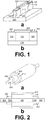
- Fig. 1 a depicts a perspective schematic view of a FinFET in accordance with an embodiment of the present invention
- Fig. 1b shows a longitudinal cross section through the FinFET.
- the FinFET comprises a semiconductor fin (110), e.g. n-doped InGaAs, on a substrate (500).
- a gate comprising a gate dielectric (410) and a gate metal (420) is present on top of a middle portion of the fin (110), defining a channel therein.
- Metallic contacts (300) connect to the source and drain regions (100) at the longitudinal ends of the fin (110).
- the first semiconductor in the source and drain regions (100) has its charge carrier concentration increased by being sandwiched between two second semiconductor structures (200), e.g. n-doped InP, which transfer charge carriers therein.
- Fig. 2a depicts a perspective schematic view of a nanowire FET in accordance with an embodiment of the present invention
- Fig. 2b shows a longitudinal cross section through the nanowire FET.
- the nanowire (120) comprises a first semiconductor, e.g. n-doped InGaAs.
- a gate comprising a gate dielectric (410) and a gate metal (420) is present around a middle portion of the nanowire (120), defining a channel therein.
- Metallic contacts (300) connect to the source and drain regions (100) around the longitudinal ends of the nanowire (120).
- the first semiconductor in the source and drain regions (100) has its charge carrier concentration increased by being in contact at the longitudinal ends with second semiconductor structures (200), e.g. n-doped InP, which transfer charge carriers therein.
Landscapes
- Engineering & Computer Science (AREA)
- Chemical & Material Sciences (AREA)
- Nanotechnology (AREA)
- Physics & Mathematics (AREA)
- Mathematical Physics (AREA)
- Theoretical Computer Science (AREA)
- Crystallography & Structural Chemistry (AREA)
- Electrodes Of Semiconductors (AREA)
- Thin Film Transistor (AREA)
- Materials Engineering (AREA)
Abstract
i. a first structure (100) made of a first doped semiconductor material of a first doping type,
ii. a metal (300) in contact with the first structure (100), and
iii. at least a second structure (200) made of a second doped semiconductor material of the first doping type in contact with the first structure (100), wherein a band off-set for majority charge carriers between the first doped semiconductor material and the second doped semiconductor material is sufficiently large for charge carriers from the second doped semiconductor material to be transferred into the first doped semiconductor material.

Description
- The present invention relates to semiconductor devices and in particular to means for increasing the charge carrier concentration in a semiconductor material in these devices.
- Metal/semiconductor contact resistance is a critical component of parasitic resistance in semiconductor devices. A typical method to reduce this contact resistance is by increasing the carrier concentration in the source/drain semiconductors. However, there is a practical upper limit to this carrier concentration using traditional doping methods. For instance, with n-type group III-V semiconductors, the upper limit of carrier concentration is usually below 1x1020 cm-3 using either in situ doping or ion implantation. Such a carrier concentration is typically insufficient to achieve a low contact resistance with the metal.
- A different approach is for example described in
U.S. Pat. N° 9,152,583 - There is thus still a need within the art for means to increase the carrier concentration in semiconductors and thereby reducing the contact resistance.
- It is an object of the present invention to provide good devices and methods for increasing the carrier concentration in semiconductors.
- It is an advantage of embodiments of the present invention that the contact resistance between a metal and the semiconductor can be lowered.
- It is an advantage of embodiments of the present invention that it is compatible with traditional doping methods.
- It is an advantage of embodiments of the present invention that the practical carrier concentration limits inherent to traditional doping methods can be surpassed.
- The above objective is accomplished by a method and device according to the present invention.
- In a first aspect, the present invention relates to a semiconductor device comprising:
- i. a first structure made of a first doped semiconductor material of a first doping type,
- ii. a metal in contact with the first structure, and
- iii. at least a second structure made of a second doped semiconductor material of the first doping type in contact with the first structure, wherein a band off-set for majority charge carriers between the first doped semiconductor material and the second doped semiconductor material is sufficiently large for charge carriers from the second doped semiconductor material to be transferred into the first doped semiconductor material.
- In a second aspect, the present invention relates to a method for reducing a contact resistance between a metal and a first structure made of a first doped semiconductor material of a first doping type, comprising:
- a. providing the first structure,
- b. providing a metal in contact with the first structure, and
- c. providing at least a second structure made of a second doped semiconductor material of the first doping type and in contact with the first structure;
- In a third aspect, the present invention relates to a use of a second structure, made of a second doped semiconductor material of a first doping type having a band off-set for majority charge carriers between a first structure made of a first doped semiconductor material of the first doping type and the second structure sufficiently large for charge carriers from the second semiconductor material to be transferred into the first semiconductor material, to reduce a contact resistance between a metal and the first structure.
- Particular and preferred aspects of the invention are set out in the accompanying independent and dependent claims. Features from the dependent claims may be combined with features of the independent claims and with features of other dependent claims as appropriate and not merely as explicitly set out in the claims.
- Although there has been constant improvement, change and evolution of devices in this field, the present concepts are believed to represent substantial new and novel improvements, including departures from prior practices, resulting in the provision of more efficient, stable and reliable devices of this nature.
- The above and other characteristics, features and advantages of the present invention will become apparent from the following detailed description, taken in conjunction with the accompanying drawings, which illustrate, by way of example, the principles of the invention. This description is given for the sake of example only, without limiting the scope of the invention. The reference figures quoted below refer to the attached drawings.
-
-
Fig. 1 shows a schematic representation of a FinFET in accordance with an embodiment of the present invention.Fig. 1(a) is a perspective view andFig. 1 (b) is a longitudinal cross-section through the perspective view ofFig. 1(a) . -
Fig. 2 shows a schematic representation of a nanowire FET in accordance with an embodiment of the present invention.Fig. 2(a) is a perspective view andFig. 2 (b) is a longitudinal cross-section through the perspective view ofFig. 2(a) . - In the different figures, the same reference signs refer to the same or analogous elements.
- The present invention will be described with respect to particular embodiments and with reference to certain drawings but the invention is not limited thereto but only by the claims. The drawings described are only schematic and are non-limiting. In the drawings, the size of some of the elements may be exaggerated and not drawn on scale for illustrative purposes. The dimensions and the relative dimensions do not correspond to actual reductions to practice of the invention.
- Furthermore, the terms first, second, third and the like in the description and in the claims, are used for distinguishing between similar elements and not necessarily for describing a sequence, either temporally, spatially, in ranking or in any other manner. It is to be understood that the terms so used are interchangeable under appropriate circumstances and that the embodiments of the invention described herein are capable of operation in other sequences than described or illustrated herein.
- Moreover, the terms top, bottom, over, under and the like in the description and the claims are used for descriptive purposes and not necessarily for describing relative positions. It is to be understood that the terms so used are interchangeable under appropriate circumstances and that the embodiments of the invention described herein are capable of operation in other orientations than described or illustrated herein.
- It is to be noticed that the term "comprising", used in the claims, should not be interpreted as being restricted to the means listed thereafter; it does not exclude other elements or steps. It is thus to be interpreted as specifying the presence of the stated features, integers, steps or components as referred to, but does not preclude the presence or addition of one or more other features, integers, steps or components, or groups thereof. Thus, the scope of the expression "a device comprising means A and B" should not be limited to devices consisting only of components A and B. It means that with respect to the present invention, the only relevant components of the device are A and B.
- Reference throughout this specification to "one embodiment" or "an embodiment" means that a particular feature, structure or characteristic described in connection with the embodiment is included in at least one embodiment of the present invention. Thus, appearances of the phrases "in one embodiment" or "in an embodiment" in various places throughout this specification are not necessarily all referring to the same embodiment, but may. Furthermore, the particular features, structures or characteristics may be combined in any suitable manner, as would be apparent to one of ordinary skill in the art from this disclosure, in one or more embodiments.
- Similarly it should be appreciated that in the description of exemplary embodiments of the invention, various features of the invention are sometimes grouped together in a single embodiment, figure, or description thereof for the purpose of streamlining the disclosure and aiding in the understanding of one or more of the various inventive aspects. This method of disclosure, however, is not to be interpreted as reflecting an intention that the claimed invention requires more features than are expressly recited in each claim. Rather, as the following claims reflect, inventive aspects lie in less than all features of a single foregoing disclosed embodiment. Thus, the claims following the detailed description are hereby expressly incorporated into this detailed description, with each claim standing on its own as a separate embodiment of this invention.
- Furthermore, while some embodiments described herein include some but not other features included in other embodiments, combinations of features of different embodiments are meant to be within the scope of the invention, and form different embodiments, as would be understood by those in the art. For example, in the following claims, any of the claimed embodiments can be used in any combination.
- Furthermore, some of the embodiments are described herein as a method or combination of elements of a method that can be implemented by a processor of a computer system or by other means of carrying out the function. Thus, a processor with the necessary instructions for carrying out such a method or element of a method forms a means for carrying out the method or element of a method. Furthermore, an element described herein of an apparatus embodiment is an example of a means for carrying out the function performed by the element for the purpose of carrying out the invention.
- In the description provided herein, numerous specific details are set forth. However, it is understood that embodiments of the invention may be practiced without these specific details. In other instances, well-known methods, structures and techniques have not been shown in detail in order not to obscure an understanding of this description.
- Reference will be made to transistors. These are devices having a first main electrode such as a drain, a second main electrode such as a source and a control electrode such as a gate for controlling the flow of electrical charges between the first and second main electrodes.
- It will be clear for a person skilled in the art that the present invention is also applicable to similar devices that can be configured in any transistor technology, including for example, but not limited thereto, CMOS, BICMOS, Bipolar and SiGe BICMOS technology. Furthermore, the findings of the present invention are explained with reference to PMOS and NMOS transistors as an example, but the present invention includes within its scope a complementary device whereby PMOS and NMOS transistors become NMOS and PMOS transistors, respectively. A skilled person can make such modifications without departing from the true technical teachings of the invention.
- The following term is provided solely to aid in the understanding of the invention.
- As used herein, the band offset between two materials is the energy gap between the conduction or valence bands of the two materials when these materials are in contact with one another, where the conduction bands are used when the majority charge carriers are electrons and the valence bands are used when the majority charge carriers are holes.
- In a first aspect, the present invention relates to a semiconductor device comprising:
- i. a first structure made of a first doped semiconductor material of a first doping type,
- ii. a metal in contact with the first structure, and
- iii. at least a second structure made of a second doped semiconductor material of the first doping type in contact with the first structure, wherein a band offset for majority charge carriers between the first doped semiconductor material and the second doped semiconductor material is sufficiently large for charge carriers from the second doped semiconductor material to be transferred into the first doped semiconductor material.
- It was surprisingly found within the present invention that a second structure of a doped semiconductor material can be used to transfer additional charge carriers into a first structure of a first doped semiconductor material. Furthermore, using this principle allows to overcome the practical charge carrier concentration limit inherent to traditional doping methods, such as in situ doping or ion implantation.
- In embodiments, the first structure may comprise at least one zone in contact with the metal, the zone having a charge carrier concentration of at least 1x1020 cm-3, preferably at least 5x1020 cm-3. For example, for III-V semiconductors, charge concentrations achieved by traditional doping methods are typically below 1x1020 cm-3.
- The first structure is not separated from the metal by the second structure.
- In embodiments, the metal is in direct contact with the first structure.
- In embodiments, the band offset for majority charge carriers is from 0.2 to 5.0 eV, preferably from 0.3 to 4.0 eV, more preferably from 0.5 to 2.0 eV. Such band offset values are typically sufficient for charge carriers to be transferred from the second doped semiconductor material to the first doped semiconductor material. The band offset can be evaluated as the energy gap between the conduction or valence bands of the first and second semiconductor as bulk materials on their own. This is the preferred method used in the present invention. Actual values for the conduction or valence bands energy levels can be taken from the literature and can for example be evaluated by the model solid theory (see E.G. Van de Walle et al., Phys. Rev. B (USA) vol.39 (1989) p.1871). For instance, the valence band energy level for Si derived in this reference was -7.03 eV and the valence band energy level for Ge derived in this reference was -6.35 eV, leading to a band offset of 0.68 eV. Other methods include modelling the energy level values based on density functional theory (DFT) or measuring them using electrical measurements (e.g. via cyclovoltametry), X-ray photoelectron spectroscopy (XPS), photoemission spectroscopy or Kelvin probe microscopy. It should be noted that absolute values of the energy levels typically depend on the technique used to obtain them, whereas relative differences are typically technique independent. Hence the band offset values have a low dependence on the technic used to evaluate them.
- Effects, such as size quantization effects that occur when the first and/or second structure have at least one dimension below 15 nm, e.g. below 10 nm, or such as interfacial chemical bonds between the first and the second structure, can alter the position of the respective energy bands as compared to their bulk values. In such cases, the evaluation of the band offset based on the bulk values may be improved by taking these effects into account in the evaluation. Methods available for that purpose are well known to the person skilled in the art and may include computations based on DFT or on (non)-parabolic analytic expressions (see e.g. J. Davies, "The Physics of Low-Dimensional Semiconductors: an introduction", Cambridge University Press, 1998.) For example for n-MOS III/V materials, quantization effects can be very strong and shifts of the conduction band 0.5 eV or more can occur. Typically, the changes induced in the energy band position due to quantization effects evolve as a function of thickness/effective mass. For light effective mass semiconductors (e.g. III/V materials), quantization effects of a few meV typically appear from a film thickness of about 14 nm, rising to around 0.1 eV for about 10 nm and further increasing to about 0.5 eV for a thickness of 4 nm. Due to their higher effective mass, the effect is present but less pronounced for Si and Ge.
- The first and second semiconductor are both doped materials of a same doping type, meaning they are both either n- or p-doped. In preferred embodiments, both the first and the second semiconductor are doped with the same dopant. Using the same dopant advantageously allows both semiconductors to be doped in a single doping step.
- The second structure, its function being to increase the charge carrier concentration in the first structure by transferring carriers therein, is typically present outside of the (main) current path of the semiconductor device. Transferring the charge carriers typically occurs upon contacting the two structures, forming a heterojunction between them, and does not require a current to be running through the semiconductor device. In embodiments, a current path may be running through the metal and the first structure without running through the second structure. This situation most typically occurs when there is no contact between the metal and the second structure. In other embodiments, an additional current path may be running through the metal and the second structure. This situation most typically occurs when the metal contacts both the first and the second structure. However, since the charge transfer (i.e. heterojunction formation) creates a considerable potential difference between the two structures, the current through the second structure will typically be small compared to the current through the first structure.
- The extent to which the second structure can increase the charge carrier concentration in the first structure will depend on both the band offset between the first and the second structure and the amount of charge carriers in the second structure, i.e. on its charge carrier concentration and on its volume. As such, the second structure is preferably highly doped, i.e. has a high charge carrier concentration (e.g. at least 1x1019 cm-3). Typically, the larger the volume ratio between the second structure and the first structure, the larger the extent to which the second structure can increase the charge carrier concentration in the first structure. The actual effect obtained for a given volume ratio typically depends on the charge carrier concentration of the second structure, and the band offset between the first and the second structure. In an embodiment, this volume ratio may be above 0.5, preferably above 1.
- Furthermore, the final charge carrier concentration in the first structure will also depend on its initial charge carrier concentration, i.e. before charge transfer from the second structure, and it is therefore also preferable for the first structure to be highly doped (e.g. at least 1x1019 cm-3).
- In embodiments, the first and/or second structure may have at least one dimension ranging from 1 to 100 nm, preferably from 5 to 20 nm; i.e. the first and/or second structure are advantageously nanostructures. In embodiments, the first semiconductor material may be p-type Ge and the second semiconductor material may be p-type Si. This selection of materials advantageously yields a first semiconductor with a high concentration of hole charge carriers. In other embodiments, the first semiconductor material may be n-type InGaAs and the second semiconductor material may be n-type InP. This selection of materials advantageously yields a first semiconductor with a high concentration of electron charge carriers.
- In embodiments, the semiconductor device may be a field-effect transistor (FET), the first structure may be a source or a drain and the metal may be a contact to the source or drain. Increasing the charge carrier concentration in the first structure and thereby reducing the contact resistance with the first metal is advantageously useful in field-effect transistors.
- In embodiments, the semiconductor device may be a Fin Field Effect Transistor (FinFET), wherein the first structure may be comprised in a fin. In embodiments, the first structure comprised in the fin may be in contact with one or more second structures on two lateral sides of the fin (see e.g. example 1). In other words, the first structure comprised in the fin may have two sidewalls, each in contact with a second structure. For instance, the first sidewall could be in contact with a first second structure and the second sidewall could be in contact with a further second structure; or the first sidewall and the second sidewall could both contact a same second structure.
- In other embodiments, the first structure may be comprised in a nanowire. In embodiments, the first structure comprised in the nanowire may be in contact with the second structure on a longitudinal end of the nanowire (see e.g. example 2). In other words, the first structure may comprise an extremity of the nanowire and that extremity may be in contact with the second structure. As a result, the first structure is between the channel and the second structure.
- In yet other embodiments, the semiconductor device may be a planar MOSFET.
- In a second aspect, the present invention relates to a method for reducing a contact resistance between a metal and a first structure made of a first doped semiconductor material of a first doping type, comprising:
- a. providing the first structure,
- b. providing a metal in contact with the first structure, and
- c. providing at least a second structure made of a second doped semiconductor material of the first doping type and in contact with the first structure;
- In embodiments, the charge carrier concentrations of the first doped semiconductor material of the first structure provided in step a and of the second structure provided in step c may be each of at least 1x1019 cm-3. It is advantageous for both semiconductors to be highly doped, in order to achieve a high charge carrier concentration in the first structure after charge transfer.
- In embodiments, the different features of the second aspect and its embodiments may independently be as correspondingly described for the first aspect and its embodiments.
- In a third aspect, the present invention relates to a use of a second structure, made of a second doped semiconductor material of a first doping type having a band offset for majority charge carriers between a first structure made of a first doped semiconductor material of the first doping type and the second structure sufficiently large for charge carriers from the second semiconductor material to be transferred into the first semiconductor material, to reduce a contact resistance between a metal and the first structure.
- In embodiments, the different features of the third aspect and its embodiments may be independently as correspondingly described for the first or second aspect and their embodiments.
- The invention will now be described by a detailed description of several embodiments of the invention. It is clear that other embodiments of the invention can be configured according to the knowledge of the person skilled in the art without departing from the true technical teaching of the invention, the invention being limited only by the terms of the appended claims.
- We now refer to
Fig. 1. Fig. 1 a depicts a perspective schematic view of a FinFET in accordance with an embodiment of the present invention,Fig. 1b shows a longitudinal cross section through the FinFET. The FinFET comprises a semiconductor fin (110), e.g. n-doped InGaAs, on a substrate (500). A gate, comprising a gate dielectric (410) and a gate metal (420) is present on top of a middle portion of the fin (110), defining a channel therein. Metallic contacts (300) connect to the source and drain regions (100) at the longitudinal ends of the fin (110). The first semiconductor in the source and drain regions (100) has its charge carrier concentration increased by being sandwiched between two second semiconductor structures (200), e.g. n-doped InP, which transfer charge carriers therein. - We now refer to
Fig. 2. Fig. 2a depicts a perspective schematic view of a nanowire FET in accordance with an embodiment of the present invention,Fig. 2b shows a longitudinal cross section through the nanowire FET. The nanowire (120) comprises a first semiconductor, e.g. n-doped InGaAs. A gate, comprising a gate dielectric (410) and a gate metal (420) is present around a middle portion of the nanowire (120), defining a channel therein. Metallic contacts (300) connect to the source and drain regions (100) around the longitudinal ends of the nanowire (120). The first semiconductor in the source and drain regions (100) has its charge carrier concentration increased by being in contact at the longitudinal ends with second semiconductor structures (200), e.g. n-doped InP, which transfer charge carriers therein. - It is to be understood that although preferred embodiments, specific constructions and configurations, as well as materials, have been discussed herein for devices according to the present invention, various changes or modifications in form and detail may be made without departing from the scope and technical teachings of this invention. For example, any formulas given above are merely representative of procedures that may be used. Functionality may be added or deleted from the block diagrams and operations may be interchanged among functional blocks. Steps may be added or deleted to methods described within the scope of the present invention.
Claims (16)
- A semiconductor device comprising:i. a first structure (100) made of a first doped semiconductor material of a first doping type,ii. a metal (300) in contact with the first structure (100), andiii. at least a second structure (200) made of a second doped semiconductor material of the first doping type in contact with the first structure (100), wherein a band offset for majority charge carriers between the first doped semiconductor material and the second doped semiconductor material is sufficiently large for charge carriers from the second doped semiconductor material to be transferred into the first doped semiconductor material.
- The semiconductor device according to claim 1 being a field-effect transistor, wherein the first structure (100) is a source or a drain and the metal (300) is a contact to the source or drain.
- The semiconductor device according to claim 2 being a Fin Field Effect Transistor, wherein the first structure (100) is comprised in a fin (110).
- The semiconductor device according to claim 3, wherein the first structure (100) comprised in the fin (110) has two sidewalls, each in contact with a second structure (200).
- The semiconductor device according to claim 2, wherein the first structure (100) is comprised in a nanowire (120).
- The semiconductor device according to claim 5, wherein the first structure (100) comprises an extremity of the nanowire (120) and wherein that extremity is in contact with the second structure (200).
- The semiconductor device according to any one of the preceding claims, wherein the band offset for majority charge carriers is from 0.2 to 5.0 eV.
- The semiconductor device according to any one of the preceding claims, wherein the first structure (100) has at least one dimension ranging from 1 to 100 nm, preferably from 5 to 20 nm.
- The semiconductor device according to any one of the preceding claims, wherein the second structure (200) has at least one dimension ranging from 1 to 100 nm, preferably from 5 to 20 nm.
- The semiconductor device according to any of the previous claims, wherein a current path is running through the metal (300) and the first structure (100) without running through the second structure (200).
- The semiconductor device according to any of the previous claims, wherein the first structure (100) comprises at least one zone in contact with the metal (300), the zone having a charge carrier concentration of at least 1x1020 cm-3.
- The semiconductor device according to any of the previous claims, wherein the first semiconductor material is p-type Ge and wherein the second semiconductor material is p-type Si.
- The semiconductor device according to any one of claims 1 to 11, wherein the first semiconductor material is n-type InGaAs and wherein the second semiconductor material is n-type InP.
- A method for reducing a contact resistance between a metal (300) and a first structure (100) made of a first doped semiconductor material of a first doping type, comprising:a. providing the first structure (100),b. providing a metal (300) in contact with the first structure (100), andc. providing at least a second structure (200) made of a second doped semiconductor material of the first doping type and in contact with the first structure (100);wherein a band offset for majority charge carriers between the first and the second doped semiconductor material is sufficiently large for charge carriers from the second semiconductor material to be transferred into the first semiconductor material.
- The method according to claim 14, wherein the charge carrier concentrations of the first doped semiconductor material of the first structure (100) provided in step a and of the second structure (200) provided is step c are each of at least 1x1019 cm-3.
- Use of a second structure (200), made of a second doped semiconductor material of a first doping type having a band offset for majority charge carriers between a first structure (100) made of a first doped semiconductor material of the first doping type and the second structure (200) sufficiently large for charge carriers from the second semiconductor material to be transferred into the first semiconductor material, to reduce a contact resistance between a metal (300) and the first structure (100).
Priority Applications (2)
| Application Number | Priority Date | Filing Date | Title |
|---|---|---|---|
| EP16194616.5A EP3312883B1 (en) | 2016-10-19 | 2016-10-19 | Semiconductor devices with increased charge carrier concentration |
| US15/787,289 US10128338B2 (en) | 2016-10-19 | 2017-10-18 | Semiconductors with increased carrier concentration |
Applications Claiming Priority (1)
| Application Number | Priority Date | Filing Date | Title |
|---|---|---|---|
| EP16194616.5A EP3312883B1 (en) | 2016-10-19 | 2016-10-19 | Semiconductor devices with increased charge carrier concentration |
Publications (2)
| Publication Number | Publication Date |
|---|---|
| EP3312883A1 true EP3312883A1 (en) | 2018-04-25 |
| EP3312883B1 EP3312883B1 (en) | 2021-12-29 |
Family
ID=57153399
Family Applications (1)
| Application Number | Title | Priority Date | Filing Date |
|---|---|---|---|
| EP16194616.5A Active EP3312883B1 (en) | 2016-10-19 | 2016-10-19 | Semiconductor devices with increased charge carrier concentration |
Country Status (2)
| Country | Link |
|---|---|
| US (1) | US10128338B2 (en) |
| EP (1) | EP3312883B1 (en) |
Citations (8)
| Publication number | Priority date | Publication date | Assignee | Title |
|---|---|---|---|---|
| US20120292665A1 (en) * | 2011-05-16 | 2012-11-22 | Fabio Alessio Marino | High performance multigate transistor |
| WO2013019329A1 (en) * | 2011-07-29 | 2013-02-07 | Hrl Laboratories, Llc | Iii-nitride metal insulator semiconductor field effect transistor |
| US20140001520A1 (en) * | 2012-06-29 | 2014-01-02 | Glenn A. Glass | Contact resistance reduced p-mos transistors employing ge-rich contact layer |
| WO2015142357A1 (en) * | 2014-03-21 | 2015-09-24 | Intel Corporation | Techniques for integration of ge-rich p-mos source/drain contacts |
| US9152583B2 (en) | 2010-12-08 | 2015-10-06 | Etron Technology, Inc. | Method for operating flash memories on a bus |
| US9287360B1 (en) * | 2015-01-07 | 2016-03-15 | International Business Machines Corporation | III-V nanowire FET with compositionally-graded channel and wide-bandgap core |
| US20160079372A1 (en) * | 2013-07-30 | 2016-03-17 | Jorge A. Kittl | Device contact structures including heterojunctions for low contact resistance |
| JP2016054215A (en) * | 2014-09-03 | 2016-04-14 | 富士通株式会社 | Compound semiconductor device and manufacturing method thereof |
Family Cites Families (4)
| Publication number | Priority date | Publication date | Assignee | Title |
|---|---|---|---|---|
| JPH09139494A (en) * | 1995-11-16 | 1997-05-27 | Mitsubishi Electric Corp | Semiconductor device manufacturing method and semiconductor device |
| AU2002359628A1 (en) * | 2001-12-06 | 2003-06-23 | Hrl Laboratories, Llc | High power-low noise microwave gan heterojunction field effet transistor |
| US20100308340A1 (en) * | 2009-06-04 | 2010-12-09 | General Electric Company | Semiconductor device having a buried channel |
| US8901537B2 (en) * | 2010-12-21 | 2014-12-02 | Intel Corporation | Transistors with high concentration of boron doped germanium |
-
2016
- 2016-10-19 EP EP16194616.5A patent/EP3312883B1/en active Active
-
2017
- 2017-10-18 US US15/787,289 patent/US10128338B2/en active Active
Patent Citations (8)
| Publication number | Priority date | Publication date | Assignee | Title |
|---|---|---|---|---|
| US9152583B2 (en) | 2010-12-08 | 2015-10-06 | Etron Technology, Inc. | Method for operating flash memories on a bus |
| US20120292665A1 (en) * | 2011-05-16 | 2012-11-22 | Fabio Alessio Marino | High performance multigate transistor |
| WO2013019329A1 (en) * | 2011-07-29 | 2013-02-07 | Hrl Laboratories, Llc | Iii-nitride metal insulator semiconductor field effect transistor |
| US20140001520A1 (en) * | 2012-06-29 | 2014-01-02 | Glenn A. Glass | Contact resistance reduced p-mos transistors employing ge-rich contact layer |
| US20160079372A1 (en) * | 2013-07-30 | 2016-03-17 | Jorge A. Kittl | Device contact structures including heterojunctions for low contact resistance |
| WO2015142357A1 (en) * | 2014-03-21 | 2015-09-24 | Intel Corporation | Techniques for integration of ge-rich p-mos source/drain contacts |
| JP2016054215A (en) * | 2014-09-03 | 2016-04-14 | 富士通株式会社 | Compound semiconductor device and manufacturing method thereof |
| US9287360B1 (en) * | 2015-01-07 | 2016-03-15 | International Business Machines Corporation | III-V nanowire FET with compositionally-graded channel and wide-bandgap core |
Non-Patent Citations (2)
| Title |
|---|
| E.G. VAN DE WALLE ET AL., PHYS. REV. B (USA, vol. 39, 1989, pages 1871 |
| J. DAVIES: "The Physics of Low-Dimensional Semiconductors: an introduction", 1998, CAMBRIDGE UNIVERSITY PRESS |
Also Published As
| Publication number | Publication date |
|---|---|
| US20180108734A1 (en) | 2018-04-19 |
| EP3312883B1 (en) | 2021-12-29 |
| US10128338B2 (en) | 2018-11-13 |
Similar Documents
| Publication | Publication Date | Title |
|---|---|---|
| Colinge et al. | Junctionless nanowire transistor (JNT): Properties and design guidelines | |
| Zhao et al. | Strained Si and SiGe nanowire tunnel FETs for logic and analog applications | |
| Vandooren et al. | Analysis of trap-assisted tunneling in vertical Si homo-junction and SiGe hetero-junction tunnel-FETs | |
| TWI610448B (en) | Vertical nanowire transistor with axial engineering semiconductor and gate metallization | |
| JP2994227B2 (en) | Layer structure for CMOS transistor using strained Si / SiGe heterostructure layer | |
| Liu et al. | Vertical GeSn nanowire MOSFETs for CMOS beyond silicon | |
| Tian et al. | New self-aligned silicon nanowire transistors on bulk substrate fabricated by epi-free compatible CMOS technology: Process integration, experimental characterization of carrier transport and low frequency noise | |
| US20140346564A1 (en) | Multi-Threshold Voltage FETs | |
| KR20080025147A (en) | Semiconductor Nanowire Transistors | |
| Kumar et al. | Comparative analysis of nanowire tunnel field effect transistor for biosensor applications | |
| Bedell et al. | Mobility scaling in short-channel length strained Ge-on-insulator P-MOSFETs | |
| Del Alamo et al. | Iii-v mosfets for future cmos | |
| Villalon et al. | Experimental investigation of the tunneling injection boosters for enhanced $ I_ {ON} $ ETSOI tunnel FET | |
| Najmzadeh et al. | Accumulation-mode gate-all-around Si nanowire nMOSFETs with sub-5 nm cross-section and high uniaxial tensile strain | |
| Saravanan et al. | Performance analysis of InAs-GaAs gate-all-around tunnel field effect transistors (GAA-TFET) for analog/RF applications | |
| US20180197780A1 (en) | Field effect transistor including strained germanium fins | |
| Sun et al. | Self-aligned III-V MOSFETs: Towards a CMOS compatible and manufacturable technology solution | |
| Lal et al. | Design and performance enhancement of gate-on-source PNPN doping–less vertical nanowire TFET | |
| EP3312883B1 (en) | Semiconductor devices with increased charge carrier concentration | |
| US11972985B2 (en) | Complementary switch element | |
| Yoon et al. | Sub-10 nm Ge/GaAs heterojunction-based tunneling field-effect transistor with vertical tunneling operation for ultra-low-power applications | |
| Moselund et al. | Complementary III–V heterostructure tunnel FETs | |
| Mathew et al. | High-performance tunnel field-effect transistors (TFETs) for future low power applications | |
| RU2626392C1 (en) | Tunnel unalloyed multi-shear field nanotransistor with contacts of schottky | |
| US20160359037A1 (en) | Germanium dual-fin field effect transistor |
Legal Events
| Date | Code | Title | Description |
|---|---|---|---|
| PUAI | Public reference made under article 153(3) epc to a published international application that has entered the european phase |
Free format text: ORIGINAL CODE: 0009012 |
|
| STAA | Information on the status of an ep patent application or granted ep patent |
Free format text: STATUS: THE APPLICATION HAS BEEN PUBLISHED |
|
| AK | Designated contracting states |
Kind code of ref document: A1 Designated state(s): AL AT BE BG CH CY CZ DE DK EE ES FI FR GB GR HR HU IE IS IT LI LT LU LV MC MK MT NL NO PL PT RO RS SE SI SK SM TR |
|
| AX | Request for extension of the european patent |
Extension state: BA ME |
|
| STAA | Information on the status of an ep patent application or granted ep patent |
Free format text: STATUS: REQUEST FOR EXAMINATION WAS MADE |
|
| 17P | Request for examination filed |
Effective date: 20181019 |
|
| RBV | Designated contracting states (corrected) |
Designated state(s): AL AT BE BG CH CY CZ DE DK EE ES FI FR GB GR HR HU IE IS IT LI LT LU LV MC MK MT NL NO PL PT RO RS SE SI SK SM TR |
|
| STAA | Information on the status of an ep patent application or granted ep patent |
Free format text: STATUS: EXAMINATION IS IN PROGRESS |
|
| 17Q | First examination report despatched |
Effective date: 20210202 |
|
| RIC1 | Information provided on ipc code assigned before grant |
Ipc: H01L 29/08 20060101AFI20210630BHEP Ipc: B82Y 10/00 20110101ALI20210630BHEP Ipc: H01L 29/06 20060101ALI20210630BHEP Ipc: H01L 29/775 20060101ALI20210630BHEP Ipc: H01L 29/78 20060101ALI20210630BHEP Ipc: H01L 29/45 20060101ALI20210630BHEP Ipc: H01L 29/417 20060101ALI20210630BHEP Ipc: H01L 29/165 20060101ALI20210630BHEP Ipc: H01L 29/205 20060101ALI20210630BHEP |
|
| GRAP | Despatch of communication of intention to grant a patent |
Free format text: ORIGINAL CODE: EPIDOSNIGR1 |
|
| STAA | Information on the status of an ep patent application or granted ep patent |
Free format text: STATUS: GRANT OF PATENT IS INTENDED |
|
| INTG | Intention to grant announced |
Effective date: 20210812 |
|
| GRAS | Grant fee paid |
Free format text: ORIGINAL CODE: EPIDOSNIGR3 |
|
| GRAA | (expected) grant |
Free format text: ORIGINAL CODE: 0009210 |
|
| STAA | Information on the status of an ep patent application or granted ep patent |
Free format text: STATUS: THE PATENT HAS BEEN GRANTED |
|
| AK | Designated contracting states |
Kind code of ref document: B1 Designated state(s): AL AT BE BG CH CY CZ DE DK EE ES FI FR GB GR HR HU IE IS IT LI LT LU LV MC MK MT NL NO PL PT RO RS SE SI SK SM TR |
|
| REG | Reference to a national code |
Ref country code: GB Ref legal event code: FG4D |
|
| REG | Reference to a national code |
Ref country code: CH Ref legal event code: EP |
|
| REG | Reference to a national code |
Ref country code: AT Ref legal event code: REF Ref document number: 1459336 Country of ref document: AT Kind code of ref document: T Effective date: 20220115 |
|
| REG | Reference to a national code |
Ref country code: IE Ref legal event code: FG4D |
|
| REG | Reference to a national code |
Ref country code: DE Ref legal event code: R096 Ref document number: 602016067769 Country of ref document: DE |
|
| REG | Reference to a national code |
Ref country code: LT Ref legal event code: MG9D |
|
| PG25 | Lapsed in a contracting state [announced via postgrant information from national office to epo] |
Ref country code: RS Free format text: LAPSE BECAUSE OF FAILURE TO SUBMIT A TRANSLATION OF THE DESCRIPTION OR TO PAY THE FEE WITHIN THE PRESCRIBED TIME-LIMIT Effective date: 20211229 Ref country code: LT Free format text: LAPSE BECAUSE OF FAILURE TO SUBMIT A TRANSLATION OF THE DESCRIPTION OR TO PAY THE FEE WITHIN THE PRESCRIBED TIME-LIMIT Effective date: 20211229 Ref country code: FI Free format text: LAPSE BECAUSE OF FAILURE TO SUBMIT A TRANSLATION OF THE DESCRIPTION OR TO PAY THE FEE WITHIN THE PRESCRIBED TIME-LIMIT Effective date: 20211229 Ref country code: BG Free format text: LAPSE BECAUSE OF FAILURE TO SUBMIT A TRANSLATION OF THE DESCRIPTION OR TO PAY THE FEE WITHIN THE PRESCRIBED TIME-LIMIT Effective date: 20220329 |
|
| REG | Reference to a national code |
Ref country code: NL Ref legal event code: MP Effective date: 20211229 |
|
| REG | Reference to a national code |
Ref country code: AT Ref legal event code: MK05 Ref document number: 1459336 Country of ref document: AT Kind code of ref document: T Effective date: 20211229 |
|
| PG25 | Lapsed in a contracting state [announced via postgrant information from national office to epo] |
Ref country code: SE Free format text: LAPSE BECAUSE OF FAILURE TO SUBMIT A TRANSLATION OF THE DESCRIPTION OR TO PAY THE FEE WITHIN THE PRESCRIBED TIME-LIMIT Effective date: 20211229 Ref country code: NO Free format text: LAPSE BECAUSE OF FAILURE TO SUBMIT A TRANSLATION OF THE DESCRIPTION OR TO PAY THE FEE WITHIN THE PRESCRIBED TIME-LIMIT Effective date: 20220329 Ref country code: LV Free format text: LAPSE BECAUSE OF FAILURE TO SUBMIT A TRANSLATION OF THE DESCRIPTION OR TO PAY THE FEE WITHIN THE PRESCRIBED TIME-LIMIT Effective date: 20211229 Ref country code: HR Free format text: LAPSE BECAUSE OF FAILURE TO SUBMIT A TRANSLATION OF THE DESCRIPTION OR TO PAY THE FEE WITHIN THE PRESCRIBED TIME-LIMIT Effective date: 20211229 Ref country code: GR Free format text: LAPSE BECAUSE OF FAILURE TO SUBMIT A TRANSLATION OF THE DESCRIPTION OR TO PAY THE FEE WITHIN THE PRESCRIBED TIME-LIMIT Effective date: 20220330 |
|
| PG25 | Lapsed in a contracting state [announced via postgrant information from national office to epo] |
Ref country code: NL Free format text: LAPSE BECAUSE OF FAILURE TO SUBMIT A TRANSLATION OF THE DESCRIPTION OR TO PAY THE FEE WITHIN THE PRESCRIBED TIME-LIMIT Effective date: 20211229 |
|
| PG25 | Lapsed in a contracting state [announced via postgrant information from national office to epo] |
Ref country code: SM Free format text: LAPSE BECAUSE OF FAILURE TO SUBMIT A TRANSLATION OF THE DESCRIPTION OR TO PAY THE FEE WITHIN THE PRESCRIBED TIME-LIMIT Effective date: 20211229 Ref country code: SK Free format text: LAPSE BECAUSE OF FAILURE TO SUBMIT A TRANSLATION OF THE DESCRIPTION OR TO PAY THE FEE WITHIN THE PRESCRIBED TIME-LIMIT Effective date: 20211229 Ref country code: RO Free format text: LAPSE BECAUSE OF FAILURE TO SUBMIT A TRANSLATION OF THE DESCRIPTION OR TO PAY THE FEE WITHIN THE PRESCRIBED TIME-LIMIT Effective date: 20211229 Ref country code: PT Free format text: LAPSE BECAUSE OF FAILURE TO SUBMIT A TRANSLATION OF THE DESCRIPTION OR TO PAY THE FEE WITHIN THE PRESCRIBED TIME-LIMIT Effective date: 20220429 Ref country code: ES Free format text: LAPSE BECAUSE OF FAILURE TO SUBMIT A TRANSLATION OF THE DESCRIPTION OR TO PAY THE FEE WITHIN THE PRESCRIBED TIME-LIMIT Effective date: 20211229 Ref country code: EE Free format text: LAPSE BECAUSE OF FAILURE TO SUBMIT A TRANSLATION OF THE DESCRIPTION OR TO PAY THE FEE WITHIN THE PRESCRIBED TIME-LIMIT Effective date: 20211229 Ref country code: CZ Free format text: LAPSE BECAUSE OF FAILURE TO SUBMIT A TRANSLATION OF THE DESCRIPTION OR TO PAY THE FEE WITHIN THE PRESCRIBED TIME-LIMIT Effective date: 20211229 |
|
| PG25 | Lapsed in a contracting state [announced via postgrant information from national office to epo] |
Ref country code: PL Free format text: LAPSE BECAUSE OF FAILURE TO SUBMIT A TRANSLATION OF THE DESCRIPTION OR TO PAY THE FEE WITHIN THE PRESCRIBED TIME-LIMIT Effective date: 20211229 Ref country code: AT Free format text: LAPSE BECAUSE OF FAILURE TO SUBMIT A TRANSLATION OF THE DESCRIPTION OR TO PAY THE FEE WITHIN THE PRESCRIBED TIME-LIMIT Effective date: 20211229 |
|
| PG25 | Lapsed in a contracting state [announced via postgrant information from national office to epo] |
Ref country code: IS Free format text: LAPSE BECAUSE OF FAILURE TO SUBMIT A TRANSLATION OF THE DESCRIPTION OR TO PAY THE FEE WITHIN THE PRESCRIBED TIME-LIMIT Effective date: 20220429 |
|
| REG | Reference to a national code |
Ref country code: DE Ref legal event code: R097 Ref document number: 602016067769 Country of ref document: DE |
|
| PG25 | Lapsed in a contracting state [announced via postgrant information from national office to epo] |
Ref country code: DK Free format text: LAPSE BECAUSE OF FAILURE TO SUBMIT A TRANSLATION OF THE DESCRIPTION OR TO PAY THE FEE WITHIN THE PRESCRIBED TIME-LIMIT Effective date: 20211229 Ref country code: AL Free format text: LAPSE BECAUSE OF FAILURE TO SUBMIT A TRANSLATION OF THE DESCRIPTION OR TO PAY THE FEE WITHIN THE PRESCRIBED TIME-LIMIT Effective date: 20211229 |
|
| PLBE | No opposition filed within time limit |
Free format text: ORIGINAL CODE: 0009261 |
|
| STAA | Information on the status of an ep patent application or granted ep patent |
Free format text: STATUS: NO OPPOSITION FILED WITHIN TIME LIMIT |
|
| 26N | No opposition filed |
Effective date: 20220930 |
|
| PG25 | Lapsed in a contracting state [announced via postgrant information from national office to epo] |
Ref country code: SI Free format text: LAPSE BECAUSE OF FAILURE TO SUBMIT A TRANSLATION OF THE DESCRIPTION OR TO PAY THE FEE WITHIN THE PRESCRIBED TIME-LIMIT Effective date: 20211229 |
|
| PG25 | Lapsed in a contracting state [announced via postgrant information from national office to epo] |
Ref country code: MC Free format text: LAPSE BECAUSE OF FAILURE TO SUBMIT A TRANSLATION OF THE DESCRIPTION OR TO PAY THE FEE WITHIN THE PRESCRIBED TIME-LIMIT Effective date: 20211229 Ref country code: IT Free format text: LAPSE BECAUSE OF FAILURE TO SUBMIT A TRANSLATION OF THE DESCRIPTION OR TO PAY THE FEE WITHIN THE PRESCRIBED TIME-LIMIT Effective date: 20211229 |
|
| REG | Reference to a national code |
Ref country code: CH Ref legal event code: PL |
|
| P01 | Opt-out of the competence of the unified patent court (upc) registered |
Effective date: 20230513 |
|
| REG | Reference to a national code |
Ref country code: BE Ref legal event code: MM Effective date: 20221031 |
|
| GBPC | Gb: european patent ceased through non-payment of renewal fee |
Effective date: 20221019 |
|
| PG25 | Lapsed in a contracting state [announced via postgrant information from national office to epo] |
Ref country code: LU Free format text: LAPSE BECAUSE OF NON-PAYMENT OF DUE FEES Effective date: 20221019 |
|
| PG25 | Lapsed in a contracting state [announced via postgrant information from national office to epo] |
Ref country code: LI Free format text: LAPSE BECAUSE OF NON-PAYMENT OF DUE FEES Effective date: 20221031 Ref country code: FR Free format text: LAPSE BECAUSE OF NON-PAYMENT OF DUE FEES Effective date: 20221031 Ref country code: CH Free format text: LAPSE BECAUSE OF NON-PAYMENT OF DUE FEES Effective date: 20221031 |
|
| PG25 | Lapsed in a contracting state [announced via postgrant information from national office to epo] |
Ref country code: BE Free format text: LAPSE BECAUSE OF NON-PAYMENT OF DUE FEES Effective date: 20221031 |
|
| PG25 | Lapsed in a contracting state [announced via postgrant information from national office to epo] |
Ref country code: IE Free format text: LAPSE BECAUSE OF NON-PAYMENT OF DUE FEES Effective date: 20221019 Ref country code: GB Free format text: LAPSE BECAUSE OF NON-PAYMENT OF DUE FEES Effective date: 20221019 |
|
| PG25 | Lapsed in a contracting state [announced via postgrant information from national office to epo] |
Ref country code: HU Free format text: LAPSE BECAUSE OF FAILURE TO SUBMIT A TRANSLATION OF THE DESCRIPTION OR TO PAY THE FEE WITHIN THE PRESCRIBED TIME-LIMIT; INVALID AB INITIO Effective date: 20161019 |
|
| PG25 | Lapsed in a contracting state [announced via postgrant information from national office to epo] |
Ref country code: CY Free format text: LAPSE BECAUSE OF FAILURE TO SUBMIT A TRANSLATION OF THE DESCRIPTION OR TO PAY THE FEE WITHIN THE PRESCRIBED TIME-LIMIT Effective date: 20211229 |
|
| PG25 | Lapsed in a contracting state [announced via postgrant information from national office to epo] |
Ref country code: MK Free format text: LAPSE BECAUSE OF FAILURE TO SUBMIT A TRANSLATION OF THE DESCRIPTION OR TO PAY THE FEE WITHIN THE PRESCRIBED TIME-LIMIT Effective date: 20211229 |
|
| PG25 | Lapsed in a contracting state [announced via postgrant information from national office to epo] |
Ref country code: TR Free format text: LAPSE BECAUSE OF FAILURE TO SUBMIT A TRANSLATION OF THE DESCRIPTION OR TO PAY THE FEE WITHIN THE PRESCRIBED TIME-LIMIT Effective date: 20211229 |
|
| PG25 | Lapsed in a contracting state [announced via postgrant information from national office to epo] |
Ref country code: MT Free format text: LAPSE BECAUSE OF FAILURE TO SUBMIT A TRANSLATION OF THE DESCRIPTION OR TO PAY THE FEE WITHIN THE PRESCRIBED TIME-LIMIT Effective date: 20211229 |
|
| REG | Reference to a national code |
Ref country code: DE Ref legal event code: R079 Ref document number: 602016067769 Country of ref document: DE Free format text: PREVIOUS MAIN CLASS: H01L0029080000 Ipc: H10D0062130000 |
|
| PGFP | Annual fee paid to national office [announced via postgrant information from national office to epo] |
Ref country code: DE Payment date: 20250923 Year of fee payment: 10 |