EP3312575A1 - Photon detection device and photon detection method - Google Patents
Photon detection device and photon detection method Download PDFInfo
- Publication number
- EP3312575A1 EP3312575A1 EP16811642.4A EP16811642A EP3312575A1 EP 3312575 A1 EP3312575 A1 EP 3312575A1 EP 16811642 A EP16811642 A EP 16811642A EP 3312575 A1 EP3312575 A1 EP 3312575A1
- Authority
- EP
- European Patent Office
- Prior art keywords
- superconducting
- photon detection
- photon
- stripline
- detection device
- Prior art date
- Legal status (The legal status is an assumption and is not a legal conclusion. Google has not performed a legal analysis and makes no representation as to the accuracy of the status listed.)
- Granted
Links
- 238000001514 detection method Methods 0.000 title claims abstract description 109
- 230000004907 flux Effects 0.000 claims abstract description 61
- 230000005291 magnetic effect Effects 0.000 claims abstract description 35
- 230000003287 optical effect Effects 0.000 claims description 13
- 238000000034 method Methods 0.000 claims description 4
- 238000010586 diagram Methods 0.000 description 15
- 238000004891 communication Methods 0.000 description 9
- 230000005292 diamagnetic effect Effects 0.000 description 9
- 230000035945 sensitivity Effects 0.000 description 9
- 239000000758 substrate Substances 0.000 description 7
- 230000005540 biological transmission Effects 0.000 description 4
- 230000004048 modification Effects 0.000 description 4
- 238000012986 modification Methods 0.000 description 4
- 230000004044 response Effects 0.000 description 4
- 230000007423 decrease Effects 0.000 description 3
- 239000000463 material Substances 0.000 description 3
- 238000012545 processing Methods 0.000 description 3
- 238000003491 array Methods 0.000 description 2
- 239000003990 capacitor Substances 0.000 description 2
- 238000007796 conventional method Methods 0.000 description 2
- 238000005259 measurement Methods 0.000 description 2
- 239000013307 optical fiber Substances 0.000 description 2
- 230000007704 transition Effects 0.000 description 2
- 229910000530 Gallium indium arsenide Inorganic materials 0.000 description 1
- 230000005668 Josephson effect Effects 0.000 description 1
- VYPSYNLAJGMNEJ-UHFFFAOYSA-N Silicium dioxide Chemical compound O=[Si]=O VYPSYNLAJGMNEJ-UHFFFAOYSA-N 0.000 description 1
- XUIMIQQOPSSXEZ-UHFFFAOYSA-N Silicon Chemical compound [Si] XUIMIQQOPSSXEZ-UHFFFAOYSA-N 0.000 description 1
- 230000002411 adverse Effects 0.000 description 1
- 230000015572 biosynthetic process Effects 0.000 description 1
- 239000004020 conductor Substances 0.000 description 1
- 239000000470 constituent Substances 0.000 description 1
- 230000008878 coupling Effects 0.000 description 1
- 238000010168 coupling process Methods 0.000 description 1
- 238000005859 coupling reaction Methods 0.000 description 1
- 230000003247 decreasing effect Effects 0.000 description 1
- 230000009977 dual effect Effects 0.000 description 1
- 230000000694 effects Effects 0.000 description 1
- 238000005516 engineering process Methods 0.000 description 1
- 230000006872 improvement Effects 0.000 description 1
- 238000004519 manufacturing process Methods 0.000 description 1
- 230000010287 polarization Effects 0.000 description 1
- 230000001902 propagating effect Effects 0.000 description 1
- 229910052710 silicon Inorganic materials 0.000 description 1
- 239000010703 silicon Substances 0.000 description 1
- 229910052814 silicon oxide Inorganic materials 0.000 description 1
- 230000000087 stabilizing effect Effects 0.000 description 1
Images


Classifications
-
- G—PHYSICS
- G01—MEASURING; TESTING
- G01J—MEASUREMENT OF INTENSITY, VELOCITY, SPECTRAL CONTENT, POLARISATION, PHASE OR PULSE CHARACTERISTICS OF INFRARED, VISIBLE OR ULTRAVIOLET LIGHT; COLORIMETRY; RADIATION PYROMETRY
- G01J1/00—Photometry, e.g. photographic exposure meter
- G01J1/42—Photometry, e.g. photographic exposure meter using electric radiation detectors
- G01J1/44—Electric circuits
-
- G—PHYSICS
- G01—MEASURING; TESTING
- G01J—MEASUREMENT OF INTENSITY, VELOCITY, SPECTRAL CONTENT, POLARISATION, PHASE OR PULSE CHARACTERISTICS OF INFRARED, VISIBLE OR ULTRAVIOLET LIGHT; COLORIMETRY; RADIATION PYROMETRY
- G01J1/00—Photometry, e.g. photographic exposure meter
- G01J1/02—Details
-
- H—ELECTRICITY
- H10—SEMICONDUCTOR DEVICES; ELECTRIC SOLID-STATE DEVICES NOT OTHERWISE PROVIDED FOR
- H10N—ELECTRIC SOLID-STATE DEVICES NOT OTHERWISE PROVIDED FOR
- H10N60/00—Superconducting devices
-
- H—ELECTRICITY
- H10—SEMICONDUCTOR DEVICES; ELECTRIC SOLID-STATE DEVICES NOT OTHERWISE PROVIDED FOR
- H10N—ELECTRIC SOLID-STATE DEVICES NOT OTHERWISE PROVIDED FOR
- H10N60/00—Superconducting devices
- H10N60/10—Junction-based devices
-
- H—ELECTRICITY
- H10—SEMICONDUCTOR DEVICES; ELECTRIC SOLID-STATE DEVICES NOT OTHERWISE PROVIDED FOR
- H10N—ELECTRIC SOLID-STATE DEVICES NOT OTHERWISE PROVIDED FOR
- H10N60/00—Superconducting devices
- H10N60/80—Constructional details
- H10N60/805—Constructional details for Josephson-effect devices
-
- H—ELECTRICITY
- H10—SEMICONDUCTOR DEVICES; ELECTRIC SOLID-STATE DEVICES NOT OTHERWISE PROVIDED FOR
- H10N—ELECTRIC SOLID-STATE DEVICES NOT OTHERWISE PROVIDED FOR
- H10N60/00—Superconducting devices
- H10N60/80—Constructional details
- H10N60/84—Switching means for devices switchable between superconducting and normal states
-
- G—PHYSICS
- G01—MEASURING; TESTING
- G01J—MEASUREMENT OF INTENSITY, VELOCITY, SPECTRAL CONTENT, POLARISATION, PHASE OR PULSE CHARACTERISTICS OF INFRARED, VISIBLE OR ULTRAVIOLET LIGHT; COLORIMETRY; RADIATION PYROMETRY
- G01J1/00—Photometry, e.g. photographic exposure meter
- G01J1/42—Photometry, e.g. photographic exposure meter using electric radiation detectors
- G01J1/44—Electric circuits
- G01J2001/4413—Type
- G01J2001/442—Single-photon detection or photon counting
-
- G—PHYSICS
- G01—MEASURING; TESTING
- G01J—MEASUREMENT OF INTENSITY, VELOCITY, SPECTRAL CONTENT, POLARISATION, PHASE OR PULSE CHARACTERISTICS OF INFRARED, VISIBLE OR ULTRAVIOLET LIGHT; COLORIMETRY; RADIATION PYROMETRY
- G01J1/00—Photometry, e.g. photographic exposure meter
- G01J1/42—Photometry, e.g. photographic exposure meter using electric radiation detectors
- G01J1/44—Electric circuits
- G01J2001/4446—Type of detector
-
- H—ELECTRICITY
- H04—ELECTRIC COMMUNICATION TECHNIQUE
- H04L—TRANSMISSION OF DIGITAL INFORMATION, e.g. TELEGRAPHIC COMMUNICATION
- H04L9/00—Cryptographic mechanisms or cryptographic arrangements for secret or secure communications; Network security protocols
- H04L9/08—Key distribution or management, e.g. generation, sharing or updating, of cryptographic keys or passwords
- H04L9/0816—Key establishment, i.e. cryptographic processes or cryptographic protocols whereby a shared secret becomes available to two or more parties, for subsequent use
- H04L9/0852—Quantum cryptography
Definitions
- an InGaAs avalanche photodiode has been widely used for photon detection in the communication wavelength band (1,550 nm), but there are problems of afterpulse generation and a large dark count. These problems are factors in increase of an error rate of key generation, but it is difficult to avoid these problems due to an operation principle of the APD.
- Non-Patent Document 1 C.M. Natarajan et al., Supercond. Sci. Technol. 25, 063001 (2012 ).
- An object of the present invention is to provide a photon detection device and a photon detection method, which solve the aforementioned various problems in the conventional techniques, are practical, can perform photon detection in which no afterpulse is generated and generation of a dark count is suppressed, and can obtain a high counting rate with low jitter.
- the SFQ pulse propagating through the JTL circuit 4 is output to the SFQ logic circuit 6, converted into digital data, and transmitted to a device under the room temperature environment by an appropriate cable.
- the signal processing can be performed with a timing jitter of 2.5 picoseconds or less.
Landscapes
- Physics & Mathematics (AREA)
- General Physics & Mathematics (AREA)
- Spectroscopy & Molecular Physics (AREA)
- Photometry And Measurement Of Optical Pulse Characteristics (AREA)
- Superconductor Devices And Manufacturing Methods Thereof (AREA)
Abstract
Description
- The present invention relates to a photon detection device and a photon detection method using a superconducting stripline.
- Securing information safety is an urgent task of the network society, and quantum cryptographic communication is expected as a core technology.
- However, the current safety key generation rate is not sufficient and not practical. To realize a practical safety key generation rate, it is essential to achieve higher performance of a photon detector, which is an urgent task.
- Conventionally, an InGaAs avalanche photodiode (APD) has been widely used for photon detection in the communication wavelength band (1,550 nm), but there are problems of afterpulse generation and a large dark count. These problems are factors in increase of an error rate of key generation, but it is difficult to avoid these problems due to an operation principle of the APD.
- Conventionally, a superconducting strip photon detector (SSPD) has also been used for photon detection (see
Patent Documents 1 and 2). As features of the SSPD, there is no afterpulse generation, and a dark count is relatively small. Accordingly, the SSPD is a major photon detector which realizes the quantum cryptographic communication. - However, it is difficult for the SSPD to achieve both high sensitivity and a low dark count rate due to an operation principle thereof.
-
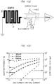
FIG. 1(a) is a diagram illustrating an equivalent circuit of a conventional SSPD photon detection device. The SSPD is a photon detection device having a superconducting stripline with a thickness of several nanometers and a width of several tens to hundreds of nanometers, and is operated by constantly flowing a bias current through the superconducting stripline. When a photon is made incident on the superconducting stripline through which the bias current flows, a complete normal conductive region is formed in a width direction of the superconducting stripline (see N inFIG. 1(a) ). Thereupon, the bias current cannot flow in a forward direction, and a current pulse is output to a measurement system. In the SSPD, this current pulse is used as a photon detection signal. - In this case, probability (quantum efficiency) of generation of the current pulse when the photon is made incident on the superconducting stripline, that is, the sensitivity depends on a magnitude of the bias current as illustrated in
FIG. 1(b) (see Non-Patent Document 1). The larger the bias current, the higher the quantum efficiency (see the left axis), but the dark count also increases at the same time (see the right axis).FIG. 1(b) is a diagram illustrating bias current dependency of quantum efficiency and bias current dependency of a dark count rate. - Thus, it is impossible to achieve both high sensitivity and a low dark count rate in the SSPD photon detection device.
- Moreover, since the current pulse is used as a principle of photon detection, it is necessary to use a low noise amplifier for amplifying the current pulse illustrated in
FIG. 1(a) . The low noise amplifier, however, adversely affects jitter of a detection system. - Furthermore, a fall time τ of the current pulse which is the principle of the photon detection is limited by a magnitude of an inductance L of the superconducting stripline. The inductance L is inversely proportional to a cross-sectional area of an entire length of the superconducting stripline. To reduce the magnitude of the inductance L, it is necessary to enlarge the cross-sectional area of the superconducting stripline. However, from the viewpoint of the sensitivity (quantum efficiency), the cross-sectional area of the superconducting stripline must be small. If the cross-sectional area is large, formation of the normal conductive region upon the incidence of the photon becomes incomplete, so that the sensitivity is lowered. For this reason, the inductance L must be increased. Accordingly, the fall of the current pulse is slow, and the fall time τ becomes long, so that a response time constant of the system becomes several tens of nanoseconds which is considered to be large, whereby a counting rate of only substantially several hundreds of megahertz is obtained.
-
- Patent Document 1:
US Unexamined Patent Application Publication No. 2005/0051726 - Patent Document 2: Japanese Patent Application Laid-Open Publication No.
2011-176159 - Non-Patent Document 1: C.M. Natarajan et al., Supercond. Sci. Technol. 25, 063001 (2012).
- An object of the present invention is to provide a photon detection device and a photon detection method, which solve the aforementioned various problems in the conventional techniques, are practical, can perform photon detection in which no afterpulse is generated and generation of a dark count is suppressed, and can obtain a high counting rate with low jitter.
- Means for solving the problems is as follows. Specifically,
- <1> A photon detection device including:
- a photon detection section including a long plate-shaped superconducting stripline whose plate surface is a photon detection surface, and bias current supply means supplying a bias current to the superconducting stripline; and
- a single flux quantum comparator circuit capable of detecting magnetic flux scattered from the superconducting stripline upon photon detection.
in which the single flux quantum comparator circuit includes at least a Josephson junction wire having a Josephson junction in the wire, and a superconducting wire electrically connecting the Josephson junction wire and the superconducting stripline, and
the superconducting stripline, the superconducting wire, and the Josephson junction wire constitute a superconducting loop capable of detecting the magnetic flux. - <3> The photon detection device according to any of <1> and <2> described above,
in which the bias current supply means is means flowing the bias current with a value of 60% to 85% of a critical current value of the superconducting stripline through the superconducting stripline. - <4> The photon detection device according to any of <1> to <3> described above,
in which the superconducting stripline is arranged on an optical waveguide through which a photon of a detection target is guided. - <5> The photon detection device according to <4> described above,
in which a plurality of the superconducting striplines are arranged along a light guiding direction of the optical waveguide, a plurality of the photon detection sections and a plurality of the single flux quantum comparator circuits are arranged for the respective superconducting striplines, and an integrated input circuit to which respective output signals output from the single flux quantum comparator circuits are integrally input is further arranged. - <6> The photon detection device according to any of <1> to <5> described above, further including:
- a time-to-digital converter measuring a time difference between an input time of a reference time signal and an input time of an output signal output from the single flux quantum comparator circuit or the integrated input circuit along with detection of the magnetic flux and converting the output signal into digital data from the time difference.
- <7> A photon detection method of detecting a photon by using the photon detection device according to any of <1> to <6> described above, the method including:
- detecting the photon by making the photon incident on a detection surface in a state where a bias current is flowed through a superconducting stripline, and detecting magnetic flux scattered from the superconducting stripline due to incidence of the photon by a single flux quantum comparator circuit.
- <8> The photon detection method according to <7> described above,
in which the bias current with a value of 60% to 85% of a critical current value of the superconducting stripline is flowed through the superconducting stripline. - According to the present invention, it is possible to provide a photon detection device and a photon detection method, which solve the aforementioned various problems in the conventional techniques, are practical, can perform photon detection in which no afterpulse is generated and generation of a dark count is suppressed, and can obtain a high counting rate with low jitter.
-
-
FIG. 1(a) is a diagram illustrating an equivalent circuit of a conventional SSPD photon detection device; -
FIG. 1(b) is a diagram illustrating bias current dependency of quantum efficiency and bias current dependency of a dark count rate; -
FIG. 2 is an explanatory diagram illustrating an outline of a first embodiment of the present invention; -
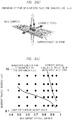
FIG. 3(a) is a diagram illustrating a result of simulating time variation of a superconducting order parameter when a photon is made incident on a superconducting stripline; -
FIG. 3(b) is an explanatory diagram illustrating an unbinding condition of a pair of magnetic flux and diamagnetic flux; -
FIG. 3(c) is a diagram illustrating a relation between a phenomenon occurring in the superconducting stripline and a bias current when a photon is incident; -
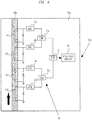
FIG. 4 is an explanatory diagram illustrating an outline of a second embodiment of the present invention; and -
FIG. 5 is an explanatory diagram illustrating an outline of a third embodiment of the present invention. - An outline of a first embodiment of the present invention is illustrated in
FIG. 2 . - A
photon detection device 10 mainly includes asuperconducting stripline 1 and a Josephson transmission line (JTL)circuit 4 serving as a single flux quantum (SFQ) circuit. - The
superconducting stripline 1 is a long plate-shaped member whose plate surface is a photon detection surface. Thissuperconducting stripline 1 is not particularly limited and may be suitably selected from known ones to be used. - Moreover, a shape of the
superconducting stripline 1 is not particularly limited. Herein, thesuperconducting stripline 1 has a linear shape for the purpose of stabilizing magnetic flux detection in theJTL circuit 4 by excluding the magnetic flux, which is excluded from thesuperconducting stripline 1, in a direction orthogonal to a length direction of the line. However, even in the case of the linear shape, this does not hinder addition of a portion with a shape other than a linear shape besides the linear portion as long as the magnetic flux excluded from the line upon incidence of a photon can be detected by theJTL circuit 4. - A line width of the
superconducting stripline 1 is not particularly limited and is generally substantially 10 nm to 200 nm, and a thickness thereof is also not particularly limited and is substantially 1 nm to 20 nm. - Also, a length of the
superconducting stripline 1 is not particularly limited and is preferably 1 µm or more and less than 10 µm and more preferably, 2 µm to 5 µm. Photon absorptance decreases if the length is less than 1 um, and current detection sensitivity in theJTL circuit 4 may decrease if the length is 10 µm or more. - A bias current is supplied to the
superconducting stripline 1. Bias current supply means supplying the bias current is not particularly limited and is, for example, means supplying a bias current with a suitable magnitude through acurrent source 2. In thephoton detection device 10, thesuperconducting stripline 1 and the bias current supply means constitute a photon detection section. - In the
photon detection device 10, aJosephson junction wire 5a, which constitutes the first stage of theJTL circuit 4 and has a Josephson junction (junction indicated by X inFIG. 2 ) in the wire, and asuperconducting wire 3, which electrically connects theJosephson junction wire 5a and thesuperconducting stripline 1, are arranged, and thesuperconducting stripline 1, thesuperconducting wire 3, and theJosephson junction wire 5a constitute a superconducting loop capable of detecting the magnetic flux. - That is, in the
photon detection device 10, thesuperconducting wire 3 and theJosephson junction wire 5a constitute an SFQ comparator circuit. - The
superconducting wire 3 is not particularly limited, and one with a relatively small capacitor may be adopted. To easily flow the bias current through thesuperconducting stripline 1, one with a relatively large capacitor may be adopted. Moreover, thesuperconducting stripline 1 and theJosephson junction wire 5a are connected with a common ground to constitute the superconducting loop. - Note that the
JTL circuit 4 is not particularly limited and can have the same configuration as a known JTL circuit. Furthermore, the Josephson junction includes a junction generating the Josephson effect, for example, a junction with a mode (weak coupling) formed by processing a portion of a superconductive material to be thinner than other portions, besides a mode in which a thin insulating film is sandwiched between two superconductive materials. - To capture the magnetic flux scattered from the
superconducting stripline 1 by the superconducting loop, thephoton detection device 10 is configured such that, for example, theJosephson junction wire 5a is arranged on an extension of thesuperconducting stripline 1 in the width direction and parallel to the length direction of the linearsuperconducting stripline 1. - Moreover, to avoid attenuation of the magnetic flux, the
Josephson junction wire 5a is preferably arranged in the vicinity of thesuperconducting stripline 1, and a distance between thesuperconducting stripline 1 and theJosephson junction wire 5a is preferably 1 µm to 10 µm as the shortest distance. - The
photon detection device 10 of a modification example may be also configured such that thesuperconducting stripline 1 and theJTL circuit 4 are provided as separate bodies without providing thesuperconducting wire 3 so as to detect the magnetic flux scattered from thesuperconducting stripline 1 with the superconducting loop in theJTL circuit 4. In this modification example, theJTL circuit 4 includes the SFQ comparator circuit. - However, when the superconducting loop is constituted by the
superconducting stripline 1, thesuperconducting wire 3, and theJosephson junction wire 5a illustrated inFIG. 2 , thesuperconducting wire 3, thesuperconducting stripline 1 which discharges the magnetic flux, and theJosephson junction wire 5a which can detect the magnetic flux as an SFQ pulse are formed as a monolithic body, in such a manner that an arrangement relation of each part is fixed, so that a photon can be stably detected, which is more practical. - Moreover, since the
superconducting stripline 1 itself constitutes the superconducting loop, the magnetic flux is easily captured, and the magnetic flux can be detected with higher detection sensitivity than the configuration of the modification example, in which the magnetic flux scattered from the outside of the superconducting loop is detected, which is more practical. - Furthermore, if the same superconductive material is used for the wires constituting the photon detection section including the
superconducting stripline 1 and for the wires constituting the comparator circuit (superconducting wire 3 andJosephson junction wire 5a), manufacturing efficiency can be improved, as well as microfabrication can be facilitated, which is more practical. - The
JTL circuit 4 is connected to anSFQ logic circuit 6. TheSFQ logic circuit 6 is not particularly limited and is, for example, a time-to-digital converter (TDC) which measures a time difference between an input time of a reference time signal and an input time of an output signal output from the SFQ comparator circuit (JTL circuit 4) along with detection of the magnetic flux and converts the output signal into digital data from the time difference. - The TDC is not particularly limited and may be suitably selected from known ones to be used. For operation in an extremely low temperature environment, the TDC is preferably an SFQ-TDC constituted by an SFQ circuit described in the following reference and developed by the inventors. The SFQ-TDC can perform signal processing with timing jitter of 2.5 picoseconds or less.
- The signal converted into the digital data by the TDC is transmitted to a device under a room temperature environment outside the device. In general, a cable which enables broadband transmission is also a good heat conductor, and thus, it is difficult to transmit an ultrafast pulse to a device under the room temperature environment. In contrast, a cable for transmitting a signal converted into digital data may be one for MHz band transmission, and by such cable, the signal can be transmitted to a device under the room temperature environment.
- Reference: K. Nakamiya, T. Nishigai, N. Yoshikawa, A. Fujimaki, H. Terai and S. Yorozu, "Improvement of time resolution of the double-oscillator time-to-digital converter using SFQ circuits," Physica C 463, 1088 (2007).
- Note that the
photon detection device 10 performs superconducting operation and thus is housed in a refrigerator or the like (not illustrated) to be used. - An operation principle and an operation method of the
photon detection device 10 will be described. - First, in the aforementioned the photon detection section, when a photon is made incident on the detection surface of the
superconducting stripline 1 in a state where the bias current is flowed, a pair of magnetic flux and diamagnetic flux is unbound. It is assumed that generation of the pair of magnetic flux and diamagnetic flux is caused by variation of a superconducting order parameter.FIG. 3(a) is a diagram illustrating a result of simulating time variation of the superconducting order parameter when a photon is made incident on the superconducting stripline. As illustrated inFIG. 3(a) , it is clear that an amplitude of the superconducting order parameter varies by substantially five picoseconds later after the photon is made incident. -
FIG. 3(b) is an explanatory diagram illustrating an unbinding condition of the pair of magnetic flux and diamagnetic flux. The pair of magnetic flux and diamagnetic flux generated in thesuperconducting stripline 1 due to the variation of the superconducting order parameter receives the Lorentz force by the bias current flowing through thesuperconducting stripline 1, and the pair of magnetic flux and diamagnetic flux is unbound. Each of the pair of magnetic flux and diamagnetic flux is excluded from thesuperconducting stripline 1 in a direction orthogonal to the flowing direction of the bias current, that is, in the width direction of thesuperconducting stripline 1, and these fluxes are scattered from thesuperconducting stripline 1. - Note that, when the bias current flowing through the
superconducting stripline 1 is sufficiently large close to the critical current at this time, a complete normal conductive region is formed in the width direction of thesuperconducting stripline 1. In the conventional SSPD, a current pulse is output by forming such a complete normal conductive region in the width direction of thesuperconducting stripline 1. In other words, this means that it is necessary to flow a sufficiently large bias current close to the critical current of thesuperconducting stripline 1. -
FIG. 3(c) is a diagram illustrating a relation between a phenomenon occurring in the superconducting stripline and the bias current when a photon is incident. As illustrated inFIG. 3(c) , it is clear that, to obtain a complete normal conductive state in the width direction of thesuperconducting stripline 1, with respect to incidence of a photon (an energy of about 1 eV) in the communication wavelength band (1550 nm), a bias current with a value of 90% or more of the critical current value is necessary (upper right region in the drawing). - In contrast, although the complete normal conductive state is not obtained in the width direction of the
superconducting stripline 1 in the region (central region in the drawing) where a bias current with a value of 85% or less of the critical current value is flowed, the pair of magnetic flux and diamagnetic flux can be generated. Moreover, the pair of magnetic flux and diamagnetic flux is not generated in the region (lower left region in the drawing) where a bias current with a value of less than 60% of the critical current value is flowed. - In the region where the bias current with a value of 90% or more of the critical current value is flowed, the superconducting order parameter is unstable, and the dark count is likely to be generated.
- In the
photon detection device 10, by flowing a bias current with a value of 60% to 85% of the critical current value of thesuperconducting stripline 1 through thesuperconducting stripline 1, the photon in the communication wavelength band can be detected without the dark count. - Description will be made with reference to
FIG. 2 again. - The magnetic flux scattered from the
superconducting stripline 1 is captured as a single flux quantum by the superconducting loop constituted by thesuperconducting stripline 1, thesuperconducting wire 3, and theJosephson junction wire 5a and generates a pulsed loop current in the superconducting loop. At this time, when a bias current is flowed through theJosephson junction wire 5a, which constitutes the first stage of theJTL circuit 4 and has the Josephson junction (junction indicated by X inFIG. 2 ) in the wire, a sum of the loop current and the bias current temporarily exceeds a critical current value of the Josephson junction of theJosephson junction wire 5a, the Josephson junction transitions to normal conduction, and the SFQ pulse is generated on theJosephson junction wire 5a. - The SFQ pulse flowing through the
Josephson junction wire 5a generates a current on the right side (output side) of the circuit. The current generated on the right side (output side) of the circuit is generated such that the current temporarily exceeds a critical current value of the Josephson junction when a bias current is flowed through aJosephson junction wire 5b constituting the second stage of theJTL circuit 4 and having a Josephson junction (junction indicated by X inFIG. 2 ) in the wire, that the Josephson junction transitions to normal conduction, and that the SFQ pulse on theJosephson junction wire 5a propagates on theJosephson junction wire 5b. Note that the response time constant of the generated SFQ pulse can be set to several picoseconds even in a general JTL circuit. - The SFQ pulse propagating through the
JTL circuit 4 is output to theSFQ logic circuit 6, converted into digital data, and transmitted to a device under the room temperature environment by an appropriate cable. By using the SFQ-TDC as theSFQ logic circuit 6, the signal processing can be performed with a timing jitter of 2.5 picoseconds or less. - Note that, although the
Josephson junction wire 5a constituting the first stage of theJTL circuit 4 has been described as a constituent member of the comparator circuit in the aforementionedphoton detection device 10, theJTL circuit 4 itself is means transmitting the SFQ pulse generated on theJosephson junction wire 5a and can be considered separately from the comparator circuit. - Therefore, a photon detection device of still another modification example may be constituted by the photon detection section including the
superconducting stripline 1, and a comparator circuit constituted by known bias current supply means supplying a bias current to theJosephson junction wire 5a and by known detection means detecting the SFQ pulse generated on theJosephson junction wire 5a, in addition to thesuperconducting wire 3 and theJosephson junction wire 5a, without having theJTL circuit 4 inFIG. 2 . - As described above, (1) since the
photon detection device 10 uses thesuperconducting stripline 1 for the photon detection, there is no afterpulse like the APD. (2) Moreover, since the device can operate with a lower bias current/critical current ratio than the SSPD, photon detection can be performed with generation of the dark count suppressed. (3) Furthermore, since a weak current pulse in thesuperconducting stripline 1 is not used as the principle of the photon detection, it is unnecessary to use a low noise amplifier (seeFIG. 1(a) ) arranged in the SSPD and possible to reduce the jitter in the measurement system in principle. (4) Further, in the SSPD, since the fall time τ of thesuperconducting stripline 1 is limited by the inductance L of the superconducting stripline (seeFIG. 1(a) ), the response time constant is set to several tens of nanoseconds, and the counting rate of the photon is only substantially several hundreds of megahertz. However, in thephoton detection device 10, the counting rate is not limited by the inductance L of thesuperconducting stripline 1, and the response time constant is determined by the time width of the magnetic flux generation (seeFIG. 3(a) ) or the fall time of the SFQ pulse (seeFIG. 2 ) and set to several picoseconds in both cases. This means that the counting rate can be improved by three orders of magnitude or more, compared to that of the SSPD. - Next, a second embodiment of the present invention will be described.
FIG. 4 is an explanatory diagram illustrating an outline of the second embodiment of the present invention. - A
photon detection device 50 is mainly constituted by monolithically forming superconducting striplines 1a to 1d,JTL circuits 4a to 4d, integrated input circuits (confluence buffer (CB)) 7a to 7c, anSFQ logic circuit 6, anoptical waveguide 8b, photon detection sections, and a comparator circuit on asubstrate 8a. Note that, since the detail of each part of the superconducting striplines 1a to 1d, theJTL circuits 4a to 4d, theSFQ logic circuit 6, the photon detection sections, and the comparator circuit is the same as that of each of thesuperconducting stripline 1, theJTL circuit 4, theSFQ logic circuit 6, the photon detection section, and the comparator circuit in thephoton detection device 10, descriptions on configuration and operation of each part are omitted. - The superconducting striplines 1a to 1d are formed on the
optical waveguide 8b. Theoptical waveguide 8b is constituted by, for example, a known silicon waveguide or the like. - As for the
optical waveguide 8b, for example, light is introduced from a lower end side in the drawing by a light supply source such as an optical fiber, and the light can be guided in an arrow direction. The light guided into theoptical waveguide 8b is made incident on the superconducting striplines 1a to 1d. - With this configuration, for example, a photon can be made incident on the superconducting stripline 1a with a higher probability than a configuration in which a photon is directly made incident on the superconducting stripline 1a by emitting the photon from a light supply source.
- Moreover, the four separate superconducting striplines 1a to 1d are arranged on the
optical waveguide 8b. - When one long large superconducting stripline is arranged in place of these superconducting striplines 1a to 1d, a photon absorptance of about 90% can be realized with a length of substantially 10 µm, and the photon absorptance is decreased by 1dB as the length is shortened by 1 µm.
- However, when such a long large superconducting stripline is used, current sensitivity in the superconducting loop may decrease. A magnitude of a loop current IL produced by the magnetic flux is expressed by the following equation, IL = Φ/L. In the equation, Φ represents a single flux quantum of 2 × 10-15 Wb, and L represents the inductance of the superconducting stripline. For the magnetic flux detection sensitivity of the JTL circuit, IL is demanded to be a certain value or more, but L becomes large if the superconducting stripline is long.
- Therefore, as illustrated in
FIG. 4 , the plurality of superconducting striplines (1a to 1d) with relatively short lengths are arranged along a light guiding direction of theoptical waveguide 8b, and these superconducting striplines with short lengths as a whole advantageously play a role of the one long superconducting stripline. - In the
photon detection device 50, the pluralities of photon detection sections (not illustrated) and JTL circuits (JTL circuits 4a to 4d) are arranged for respective superconducting striplines 1a to 1d. Further, the CB circuit 7a to which respective output signals output from theJTL circuits CB circuit 7b to which respective output signals output from theJTL circuits CB circuit 7c to which respective output signals output from theCB circuits 7a and 7b are integrally input is arranged. The superconducting striplines 1a to 1d, theJTL circuits 4a to 4d, the CB circuits 7a to 7c, theSFQ logic circuit 6, and theoptical waveguide 8b constitute one monolithicphoton detection array 9. - Each of the CB circuits 7a to 7c can be constituted by suitably selecting a circuit configuration used in a known SFQ circuit.
- Note that, as the
substrate 8a, for example, a known substrate such as a silicon oxide substrate can be used. Moreover, the digital data output from theSFQ logic circuit 6 is transmitted to a device under the room temperature environment by a cable (not illustrated) or the like. - In the
photon detection device 50 constituted in this way, if a photon can be absorbed by at least one of the superconducting striplines 1a to 1d, the photon can be detected, and the photon detection efficiency can be dramatically improved. - Next, a third embodiment of the present invention will be described.
FIG. 5 is an explanatory diagram illustrating an outline of the third embodiment of the present invention. - A
photon detection device 100 illustrated inFIG. 5 is constituted as a monolithic device in which a plurality ofphoton detection arrays 9 in thephoton detection device 50 illustrated inFIG. 4 are arranged on the same substrate. Other than this, thephoton detection device 100 is the same as thephoton detection device 50, and thus, description thereof is omitted. - According to this
photon detection device 100, a photon from a light supply source such as an independent optical fiber or the like can be independently detected by eachphoton detection array 9, and communication signals from a plurality of information sources can be processed. For example, in a setup of polarization (4) × dual wavelength multiplexing (2) × transmission/reception (2), which is the basic setup of quantum entangled quantum cryptographic communication, 16 communication signals in total are demanded to be processed independently. If 16photon detection arrays 9 are arranged on the same substrate, the device can be applied to such a communication field. -
- 1, 1a to 1d Superconducting stripline
- 2 Current source
- 3 Superconducting wire
- 4, 4a to 4d JTL circuit
- 5a, 5b Josephson junction wire
- 6 SFQ logic circuit
- 7a to 7c CB circuit
- 8a Substrate
- 8b Optical waveguide
- 9 Photon detection array
- 10, 50, 100 Photon detection device
Claims (8)
- A photon detection device comprising:a photon detection section including a long plate-shaped superconducting stripline whose plate surface is a photon detection surface, and bias current supply means supplying a bias current to the superconducting stripline; anda single flux quantum comparator circuit capable of detecting magnetic flux scattered from the superconducting stripline upon photon detection.
- The photon detection device according to claim 1,
wherein the single flux quantum comparator circuit includes at least a Josephson junction wire having a Josephson junction in the wire, and a superconducting wire electrically connecting the Josephson junction wire and the superconducting stripline, and
the superconducting stripline, the superconducting wire, and the Josephson junction wire constitute a superconducting loop capable of detecting the magnetic flux. - The photon detection device according to any of claims 1 and 2,
wherein the bias current supply means is means flowing the bias current with a value of 60% to 85% of a critical current value of the superconducting stripline through the superconducting stripline. - The photon detection device according to any of claims 1 to 3,
wherein the superconducting stripline is arranged on an optical waveguide through which a photon of a detection target is guided. - The photon detection device according to claim 4,
wherein a plurality of the superconducting striplines are arranged along a light guiding direction of the optical waveguide, a plurality of the photon detection sections and a plurality of the single flux quantum comparator circuits are arranged for the respective superconducting striplines, and an integrated input circuit to which respective output signals output from the single flux quantum comparator circuits are integrally input is further arranged. - The photon detection device according to any of claims 1 to 5, further comprising:a time-to-digital converter measuring a time difference between an input time of a reference time signal and an input time of an output signal output from the single flux quantum comparator circuit or the integrated input circuit along with detection of the magnetic flux and converting the output signal into digital data from the time difference.
- A photon detection method of detecting a photon by using the photon detection device according to any of claims 1 to 6, the method comprising:detecting the photon by making the photon incident on a detection surface in a state where a bias current is flowed through a superconducting stripline, and detecting magnetic flux scattered from the superconducting stripline due to incidence of the photon by a single flux quantum comparator circuit.
- The photon detection method according to claim 7,
wherein the bias current with a value of 60% to 85% of a critical current value of the superconducting stripline is flowed through the superconducting stripline.
Applications Claiming Priority (2)
| Application Number | Priority Date | Filing Date | Title |
|---|---|---|---|
| JP2015123764A JP6528042B2 (en) | 2015-06-19 | 2015-06-19 | Photon detection device and photon detection method |
| PCT/JP2016/067747 WO2016204168A1 (en) | 2015-06-19 | 2016-06-15 | Photon detection device and photon detection method |
Publications (3)
| Publication Number | Publication Date |
|---|---|
| EP3312575A1 true EP3312575A1 (en) | 2018-04-25 |
| EP3312575A4 EP3312575A4 (en) | 2019-03-20 |
| EP3312575B1 EP3312575B1 (en) | 2020-08-05 |
Family
ID=57545286
Family Applications (1)
| Application Number | Title | Priority Date | Filing Date |
|---|---|---|---|
| EP16811642.4A Active EP3312575B1 (en) | 2015-06-19 | 2016-06-15 | Photon detection device and photon detection method |
Country Status (5)
| Country | Link |
|---|---|
| US (1) | US10605655B2 (en) |
| EP (1) | EP3312575B1 (en) |
| JP (1) | JP6528042B2 (en) |
| CN (1) | CN107735655B (en) |
| WO (1) | WO2016204168A1 (en) |
Families Citing this family (8)
| Publication number | Priority date | Publication date | Assignee | Title |
|---|---|---|---|---|
| JP7143130B2 (en) | 2018-07-04 | 2022-09-28 | キオクシア株式会社 | Superconducting strip, particle detector and particle detection method |
| JP7066554B2 (en) * | 2018-07-04 | 2022-05-13 | キオクシア株式会社 | Superconducting strips, particle detectors and particle detection methods |
| JP7062547B2 (en) | 2018-07-25 | 2022-05-06 | キオクシア株式会社 | Particle detector, image generator and image generation method |
| CN109921903B (en) * | 2019-03-26 | 2021-10-01 | 北京信而泰科技股份有限公司 | System, method and device for detecting quantum key code rate authenticity |
| FI129128B (en) * | 2020-02-04 | 2021-07-30 | Teknologian Tutkimuskeskus Vtt Oy | Self-restoring microwave detector for a flux quantum |
| AU2022289736A1 (en) | 2021-06-11 | 2024-02-01 | Caleb JORDAN | System and method of flux bias for superconducting quantum circuits |
| DE102021119983A1 (en) * | 2021-08-02 | 2023-02-02 | Pixel Photonics GmbH | Tap-proof single photon detector device for detecting an optical signal |
| US12562738B2 (en) | 2024-04-29 | 2026-02-24 | International Business Machines Corporation | Superconducting radio frequency signal generators |
Family Cites Families (9)
| Publication number | Priority date | Publication date | Assignee | Title |
|---|---|---|---|---|
| US3149299A (en) * | 1961-03-28 | 1964-09-15 | Little Inc A | Electronic devices and process for forming same |
| US6812464B1 (en) | 2000-07-28 | 2004-11-02 | Credence Systems Corporation | Superconducting single photon detector |
| JP4101563B2 (en) * | 2002-06-14 | 2008-06-18 | ジヤトコ株式会社 | Slip prevention device for continuously variable transmission for vehicle |
| JP5158920B2 (en) * | 2003-06-06 | 2013-03-06 | 独立行政法人科学技術振興機構 | Light-magnetic flux conversion type input interface circuit |
| CN101339077A (en) | 2008-05-14 | 2009-01-07 | 南京大学 | A single photon detector based on superconducting thin film material and its manufacturing method |
| JP5470654B2 (en) | 2010-02-25 | 2014-04-16 | 独立行政法人情報通信研究機構 | Mounting method of superconducting single photon detector |
| US8971977B2 (en) * | 2011-01-17 | 2015-03-03 | Hypres, Inc. | Superconducting devices with ferromagnetic barrier junctions |
| JP5846626B2 (en) * | 2011-07-12 | 2016-01-20 | 国立研究開発法人情報通信研究機構 | Superconducting single photon detection system and superconducting single photon detection method |
| EP2740262B1 (en) | 2011-08-03 | 2020-09-09 | Koninklijke Philips N.V. | Position-sensitive readout modes for digital silicon photomultiplier arrays |
-
2015
- 2015-06-19 JP JP2015123764A patent/JP6528042B2/en active Active
-
2016
- 2016-06-15 WO PCT/JP2016/067747 patent/WO2016204168A1/en not_active Ceased
- 2016-06-15 EP EP16811642.4A patent/EP3312575B1/en active Active
- 2016-06-15 CN CN201680035554.2A patent/CN107735655B/en not_active Expired - Fee Related
- 2016-06-15 US US15/736,381 patent/US10605655B2/en active Active
Also Published As
| Publication number | Publication date |
|---|---|
| CN107735655B (en) | 2020-03-10 |
| JP2017009372A (en) | 2017-01-12 |
| US10605655B2 (en) | 2020-03-31 |
| WO2016204168A1 (en) | 2016-12-22 |
| CN107735655A (en) | 2018-02-23 |
| US20180188107A1 (en) | 2018-07-05 |
| EP3312575A4 (en) | 2019-03-20 |
| EP3312575B1 (en) | 2020-08-05 |
| JP6528042B2 (en) | 2019-06-12 |
Similar Documents
| Publication | Publication Date | Title |
|---|---|---|
| EP3312575B1 (en) | Photon detection device and photon detection method | |
| Craiciu et al. | High-speed detection of 1550 nm single photons with superconducting nanowire detectors | |
| Wolff et al. | Broadband waveguide-integrated superconducting single-photon detectors with high system detection efficiency | |
| Sprengers et al. | Waveguide superconducting single-photon detectors for integrated quantum photonic circuits | |
| Colangelo et al. | Impedance-matched differential superconducting nanowire detectors | |
| US20130143744A1 (en) | Superconducting nanowire avalanche photodetectors (snaps) with fast reset time | |
| JP5846626B2 (en) | Superconducting single photon detection system and superconducting single photon detection method | |
| US20210328126A1 (en) | Optical detection apparatus and method | |
| US12339163B1 (en) | Scalable photon number resolving photon detector | |
| Fu et al. | Multiple data streams over a single optical path | |
| Goltsman et al. | Ultrafast superconducting single-photon detector | |
| JP6684400B2 (en) | Superconducting single photon detector | |
| Santavicca et al. | Jitter characterization of a dual-readout snspd | |
| Yamashita et al. | Crosstalk-free operation of multi-element SSPD array integrated with SFQ circuit in a 0.1 Watt GM cryocooler | |
| JP2018100946A (en) | Photon detection apparatus and photon detection method | |
| US12320698B2 (en) | Interception-proof single-photon detector device for detecting an optical signal | |
| CN114865264B (en) | Double-superconducting-wire coupler | |
| JP2931787B2 (en) | Superconducting circuit | |
| Mattioli et al. | Waveguide-integrated niobium-nitride detectors for on-chip quantum nanophotonics | |
| Shiu et al. | A simple monolithically integrated optical receiver consisting of an optical preamplifier and a pin photodiode | |
| Farr et al. | Gigahertz bandwidth photon counting | |
| Słysz et al. | Fibre-coupled, single photon detector based on NbN superconducting nanostructures for quantum communications | |
| JP4389089B2 (en) | Optical signal processing device and optical signal processing method | |
| EP4683487A1 (en) | Signal processing circuit and signal processing method | |
| Miki et al. | Development of fiber-coupled four-element superconducting nanowire single-photon detectors |
Legal Events
| Date | Code | Title | Description |
|---|---|---|---|
| STAA | Information on the status of an ep patent application or granted ep patent |
Free format text: STATUS: THE INTERNATIONAL PUBLICATION HAS BEEN MADE |
|
| PUAI | Public reference made under article 153(3) epc to a published international application that has entered the european phase |
Free format text: ORIGINAL CODE: 0009012 |
|
| STAA | Information on the status of an ep patent application or granted ep patent |
Free format text: STATUS: REQUEST FOR EXAMINATION WAS MADE |
|
| 17P | Request for examination filed |
Effective date: 20171218 |
|
| AK | Designated contracting states |
Kind code of ref document: A1 Designated state(s): AL AT BE BG CH CY CZ DE DK EE ES FI FR GB GR HR HU IE IS IT LI LT LU LV MC MK MT NL NO PL PT RO RS SE SI SK SM TR |
|
| AX | Request for extension of the european patent |
Extension state: BA ME |
|
| DAV | Request for validation of the european patent (deleted) | ||
| DAX | Request for extension of the european patent (deleted) | ||
| A4 | Supplementary search report drawn up and despatched |
Effective date: 20190220 |
|
| RIC1 | Information provided on ipc code assigned before grant |
Ipc: H01L 39/00 20060101ALI20190214BHEP Ipc: G01J 1/02 20060101AFI20190214BHEP |
|
| REG | Reference to a national code |
Ref country code: DE Ref legal event code: R079 Ref document number: 602016041528 Country of ref document: DE Free format text: PREVIOUS MAIN CLASS: G01J0001020000 Ipc: G01J0001440000 |
|
| RIC1 | Information provided on ipc code assigned before grant |
Ipc: G01J 1/44 20060101AFI20191212BHEP Ipc: H01L 39/22 20060101ALI20191212BHEP |
|
| GRAP | Despatch of communication of intention to grant a patent |
Free format text: ORIGINAL CODE: EPIDOSNIGR1 |
|
| STAA | Information on the status of an ep patent application or granted ep patent |
Free format text: STATUS: GRANT OF PATENT IS INTENDED |
|
| INTG | Intention to grant announced |
Effective date: 20200213 |
|
| GRAS | Grant fee paid |
Free format text: ORIGINAL CODE: EPIDOSNIGR3 |
|
| GRAA | (expected) grant |
Free format text: ORIGINAL CODE: 0009210 |
|
| STAA | Information on the status of an ep patent application or granted ep patent |
Free format text: STATUS: THE PATENT HAS BEEN GRANTED |
|
| AK | Designated contracting states |
Kind code of ref document: B1 Designated state(s): AL AT BE BG CH CY CZ DE DK EE ES FI FR GB GR HR HU IE IS IT LI LT LU LV MC MK MT NL NO PL PT RO RS SE SI SK SM TR |
|
| REG | Reference to a national code |
Ref country code: GB Ref legal event code: FG4D |
|
| REG | Reference to a national code |
Ref country code: CH Ref legal event code: EP |
|
| REG | Reference to a national code |
Ref country code: AT Ref legal event code: REF Ref document number: 1299363 Country of ref document: AT Kind code of ref document: T Effective date: 20200815 |
|
| REG | Reference to a national code |
Ref country code: DE Ref legal event code: R096 Ref document number: 602016041528 Country of ref document: DE |
|
| REG | Reference to a national code |
Ref country code: IE Ref legal event code: FG4D |
|
| REG | Reference to a national code |
Ref country code: CH Ref legal event code: NV Representative=s name: RIEDERER HASLER AND PARTNER PATENTANWAELTE AG, LI |
|
| REG | Reference to a national code |
Ref country code: LT Ref legal event code: MG4D |
|
| REG | Reference to a national code |
Ref country code: NL Ref legal event code: MP Effective date: 20200805 |
|
| REG | Reference to a national code |
Ref country code: AT Ref legal event code: MK05 Ref document number: 1299363 Country of ref document: AT Kind code of ref document: T Effective date: 20200805 |
|
| PG25 | Lapsed in a contracting state [announced via postgrant information from national office to epo] |
Ref country code: FI Free format text: LAPSE BECAUSE OF FAILURE TO SUBMIT A TRANSLATION OF THE DESCRIPTION OR TO PAY THE FEE WITHIN THE PRESCRIBED TIME-LIMIT Effective date: 20200805 Ref country code: LT Free format text: LAPSE BECAUSE OF FAILURE TO SUBMIT A TRANSLATION OF THE DESCRIPTION OR TO PAY THE FEE WITHIN THE PRESCRIBED TIME-LIMIT Effective date: 20200805 Ref country code: AT Free format text: LAPSE BECAUSE OF FAILURE TO SUBMIT A TRANSLATION OF THE DESCRIPTION OR TO PAY THE FEE WITHIN THE PRESCRIBED TIME-LIMIT Effective date: 20200805 Ref country code: BG Free format text: LAPSE BECAUSE OF FAILURE TO SUBMIT A TRANSLATION OF THE DESCRIPTION OR TO PAY THE FEE WITHIN THE PRESCRIBED TIME-LIMIT Effective date: 20201105 Ref country code: NO Free format text: LAPSE BECAUSE OF FAILURE TO SUBMIT A TRANSLATION OF THE DESCRIPTION OR TO PAY THE FEE WITHIN THE PRESCRIBED TIME-LIMIT Effective date: 20201105 Ref country code: PT Free format text: LAPSE BECAUSE OF FAILURE TO SUBMIT A TRANSLATION OF THE DESCRIPTION OR TO PAY THE FEE WITHIN THE PRESCRIBED TIME-LIMIT Effective date: 20201207 Ref country code: GR Free format text: LAPSE BECAUSE OF FAILURE TO SUBMIT A TRANSLATION OF THE DESCRIPTION OR TO PAY THE FEE WITHIN THE PRESCRIBED TIME-LIMIT Effective date: 20201106 Ref country code: ES Free format text: LAPSE BECAUSE OF FAILURE TO SUBMIT A TRANSLATION OF THE DESCRIPTION OR TO PAY THE FEE WITHIN THE PRESCRIBED TIME-LIMIT Effective date: 20200805 Ref country code: SE Free format text: LAPSE BECAUSE OF FAILURE TO SUBMIT A TRANSLATION OF THE DESCRIPTION OR TO PAY THE FEE WITHIN THE PRESCRIBED TIME-LIMIT Effective date: 20200805 Ref country code: HR Free format text: LAPSE BECAUSE OF FAILURE TO SUBMIT A TRANSLATION OF THE DESCRIPTION OR TO PAY THE FEE WITHIN THE PRESCRIBED TIME-LIMIT Effective date: 20200805 |
|
| PG25 | Lapsed in a contracting state [announced via postgrant information from national office to epo] |
Ref country code: PL Free format text: LAPSE BECAUSE OF FAILURE TO SUBMIT A TRANSLATION OF THE DESCRIPTION OR TO PAY THE FEE WITHIN THE PRESCRIBED TIME-LIMIT Effective date: 20200805 Ref country code: RS Free format text: LAPSE BECAUSE OF FAILURE TO SUBMIT A TRANSLATION OF THE DESCRIPTION OR TO PAY THE FEE WITHIN THE PRESCRIBED TIME-LIMIT Effective date: 20200805 Ref country code: LV Free format text: LAPSE BECAUSE OF FAILURE TO SUBMIT A TRANSLATION OF THE DESCRIPTION OR TO PAY THE FEE WITHIN THE PRESCRIBED TIME-LIMIT Effective date: 20200805 Ref country code: NL Free format text: LAPSE BECAUSE OF FAILURE TO SUBMIT A TRANSLATION OF THE DESCRIPTION OR TO PAY THE FEE WITHIN THE PRESCRIBED TIME-LIMIT Effective date: 20200805 Ref country code: IS Free format text: LAPSE BECAUSE OF FAILURE TO SUBMIT A TRANSLATION OF THE DESCRIPTION OR TO PAY THE FEE WITHIN THE PRESCRIBED TIME-LIMIT Effective date: 20201205 |
|
| PG25 | Lapsed in a contracting state [announced via postgrant information from national office to epo] |
Ref country code: CZ Free format text: LAPSE BECAUSE OF FAILURE TO SUBMIT A TRANSLATION OF THE DESCRIPTION OR TO PAY THE FEE WITHIN THE PRESCRIBED TIME-LIMIT Effective date: 20200805 Ref country code: DK Free format text: LAPSE BECAUSE OF FAILURE TO SUBMIT A TRANSLATION OF THE DESCRIPTION OR TO PAY THE FEE WITHIN THE PRESCRIBED TIME-LIMIT Effective date: 20200805 Ref country code: RO Free format text: LAPSE BECAUSE OF FAILURE TO SUBMIT A TRANSLATION OF THE DESCRIPTION OR TO PAY THE FEE WITHIN THE PRESCRIBED TIME-LIMIT Effective date: 20200805 Ref country code: EE Free format text: LAPSE BECAUSE OF FAILURE TO SUBMIT A TRANSLATION OF THE DESCRIPTION OR TO PAY THE FEE WITHIN THE PRESCRIBED TIME-LIMIT Effective date: 20200805 Ref country code: SM Free format text: LAPSE BECAUSE OF FAILURE TO SUBMIT A TRANSLATION OF THE DESCRIPTION OR TO PAY THE FEE WITHIN THE PRESCRIBED TIME-LIMIT Effective date: 20200805 |
|
| REG | Reference to a national code |
Ref country code: DE Ref legal event code: R097 Ref document number: 602016041528 Country of ref document: DE |
|
| PG25 | Lapsed in a contracting state [announced via postgrant information from national office to epo] |
Ref country code: AL Free format text: LAPSE BECAUSE OF FAILURE TO SUBMIT A TRANSLATION OF THE DESCRIPTION OR TO PAY THE FEE WITHIN THE PRESCRIBED TIME-LIMIT Effective date: 20200805 |
|
| PLBE | No opposition filed within time limit |
Free format text: ORIGINAL CODE: 0009261 |
|
| STAA | Information on the status of an ep patent application or granted ep patent |
Free format text: STATUS: NO OPPOSITION FILED WITHIN TIME LIMIT |
|
| PG25 | Lapsed in a contracting state [announced via postgrant information from national office to epo] |
Ref country code: SK Free format text: LAPSE BECAUSE OF FAILURE TO SUBMIT A TRANSLATION OF THE DESCRIPTION OR TO PAY THE FEE WITHIN THE PRESCRIBED TIME-LIMIT Effective date: 20200805 |
|
| 26N | No opposition filed |
Effective date: 20210507 |
|
| PG25 | Lapsed in a contracting state [announced via postgrant information from national office to epo] |
Ref country code: IT Free format text: LAPSE BECAUSE OF FAILURE TO SUBMIT A TRANSLATION OF THE DESCRIPTION OR TO PAY THE FEE WITHIN THE PRESCRIBED TIME-LIMIT Effective date: 20200805 |
|
| PG25 | Lapsed in a contracting state [announced via postgrant information from national office to epo] |
Ref country code: SI Free format text: LAPSE BECAUSE OF FAILURE TO SUBMIT A TRANSLATION OF THE DESCRIPTION OR TO PAY THE FEE WITHIN THE PRESCRIBED TIME-LIMIT Effective date: 20200805 |
|
| PG25 | Lapsed in a contracting state [announced via postgrant information from national office to epo] |
Ref country code: MC Free format text: LAPSE BECAUSE OF FAILURE TO SUBMIT A TRANSLATION OF THE DESCRIPTION OR TO PAY THE FEE WITHIN THE PRESCRIBED TIME-LIMIT Effective date: 20200805 |
|
| GBPC | Gb: european patent ceased through non-payment of renewal fee |
Effective date: 20210615 |
|
| REG | Reference to a national code |
Ref country code: BE Ref legal event code: MM Effective date: 20210630 |
|
| PG25 | Lapsed in a contracting state [announced via postgrant information from national office to epo] |
Ref country code: LU Free format text: LAPSE BECAUSE OF NON-PAYMENT OF DUE FEES Effective date: 20210615 |
|
| PG25 | Lapsed in a contracting state [announced via postgrant information from national office to epo] |
Ref country code: IE Free format text: LAPSE BECAUSE OF NON-PAYMENT OF DUE FEES Effective date: 20210615 Ref country code: GB Free format text: LAPSE BECAUSE OF NON-PAYMENT OF DUE FEES Effective date: 20210615 |
|
| PG25 | Lapsed in a contracting state [announced via postgrant information from national office to epo] |
Ref country code: FR Free format text: LAPSE BECAUSE OF NON-PAYMENT OF DUE FEES Effective date: 20210630 |
|
| PG25 | Lapsed in a contracting state [announced via postgrant information from national office to epo] |
Ref country code: BE Free format text: LAPSE BECAUSE OF NON-PAYMENT OF DUE FEES Effective date: 20210630 |
|
| PGFP | Annual fee paid to national office [announced via postgrant information from national office to epo] |
Ref country code: DE Payment date: 20220420 Year of fee payment: 7 |
|
| PGFP | Annual fee paid to national office [announced via postgrant information from national office to epo] |
Ref country code: CH Payment date: 20220702 Year of fee payment: 7 |
|
| PG25 | Lapsed in a contracting state [announced via postgrant information from national office to epo] |
Ref country code: CY Free format text: LAPSE BECAUSE OF FAILURE TO SUBMIT A TRANSLATION OF THE DESCRIPTION OR TO PAY THE FEE WITHIN THE PRESCRIBED TIME-LIMIT Effective date: 20200805 |
|
| PG25 | Lapsed in a contracting state [announced via postgrant information from national office to epo] |
Ref country code: HU Free format text: LAPSE BECAUSE OF FAILURE TO SUBMIT A TRANSLATION OF THE DESCRIPTION OR TO PAY THE FEE WITHIN THE PRESCRIBED TIME-LIMIT; INVALID AB INITIO Effective date: 20160615 |
|
| REG | Reference to a national code |
Ref country code: DE Ref legal event code: R119 Ref document number: 602016041528 Country of ref document: DE |
|
| REG | Reference to a national code |
Ref country code: CH Ref legal event code: PL |
|
| PG25 | Lapsed in a contracting state [announced via postgrant information from national office to epo] |
Ref country code: MK Free format text: LAPSE BECAUSE OF FAILURE TO SUBMIT A TRANSLATION OF THE DESCRIPTION OR TO PAY THE FEE WITHIN THE PRESCRIBED TIME-LIMIT Effective date: 20200805 Ref country code: DE Free format text: LAPSE BECAUSE OF NON-PAYMENT OF DUE FEES Effective date: 20240103 Ref country code: CH Free format text: LAPSE BECAUSE OF NON-PAYMENT OF DUE FEES Effective date: 20230630 |
|
| PG25 | Lapsed in a contracting state [announced via postgrant information from national office to epo] |
Ref country code: TR Free format text: LAPSE BECAUSE OF FAILURE TO SUBMIT A TRANSLATION OF THE DESCRIPTION OR TO PAY THE FEE WITHIN THE PRESCRIBED TIME-LIMIT Effective date: 20200805 |
|
| PG25 | Lapsed in a contracting state [announced via postgrant information from national office to epo] |
Ref country code: MT Free format text: LAPSE BECAUSE OF FAILURE TO SUBMIT A TRANSLATION OF THE DESCRIPTION OR TO PAY THE FEE WITHIN THE PRESCRIBED TIME-LIMIT Effective date: 20200805 |