EP3312137A1 - Deposition of graphene layers by means of plasma-enhanced chemical vapour deposition - Google Patents
Deposition of graphene layers by means of plasma-enhanced chemical vapour deposition Download PDFInfo
- Publication number
- EP3312137A1 EP3312137A1 EP16811071.6A EP16811071A EP3312137A1 EP 3312137 A1 EP3312137 A1 EP 3312137A1 EP 16811071 A EP16811071 A EP 16811071A EP 3312137 A1 EP3312137 A1 EP 3312137A1
- Authority
- EP
- European Patent Office
- Prior art keywords
- substrate
- graphene
- plasma
- process according
- component
- Prior art date
- Legal status (The legal status is an assumption and is not a legal conclusion. Google has not performed a legal analysis and makes no representation as to the accuracy of the status listed.)
- Granted
Links
Images



Classifications
-
- B—PERFORMING OPERATIONS; TRANSPORTING
- B82—NANOTECHNOLOGY
- B82Y—SPECIFIC USES OR APPLICATIONS OF NANOSTRUCTURES; MEASUREMENT OR ANALYSIS OF NANOSTRUCTURES; MANUFACTURE OR TREATMENT OF NANOSTRUCTURES
- B82Y30/00—Nanotechnology for materials or surface science, e.g. nanocomposites
-
- B—PERFORMING OPERATIONS; TRANSPORTING
- B82—NANOTECHNOLOGY
- B82Y—SPECIFIC USES OR APPLICATIONS OF NANOSTRUCTURES; MEASUREMENT OR ANALYSIS OF NANOSTRUCTURES; MANUFACTURE OR TREATMENT OF NANOSTRUCTURES
- B82Y40/00—Manufacture or treatment of nanostructures
-
- C—CHEMISTRY; METALLURGY
- C01—INORGANIC CHEMISTRY
- C01B—NON-METALLIC ELEMENTS; COMPOUNDS THEREOF; METALLOIDS OR COMPOUNDS THEREOF NOT COVERED BY SUBCLASS C01C
- C01B32/00—Carbon; Compounds thereof
- C01B32/05—Preparation or purification of carbon not covered by groups C01B32/15, C01B32/20, C01B32/25, C01B32/30
-
- C—CHEMISTRY; METALLURGY
- C09—DYES; PAINTS; POLISHES; NATURAL RESINS; ADHESIVES; COMPOSITIONS NOT OTHERWISE PROVIDED FOR; APPLICATIONS OF MATERIALS NOT OTHERWISE PROVIDED FOR
- C09D—COATING COMPOSITIONS, e.g. PAINTS, VARNISHES OR LACQUERS; FILLING PASTES; CHEMICAL PAINT OR INK REMOVERS; INKS; CORRECTING FLUIDS; WOODSTAINS; PASTES OR SOLIDS FOR COLOURING OR PRINTING; USE OF MATERIALS THEREFOR
- C09D1/00—Coating compositions, e.g. paints, varnishes or lacquers, based on inorganic substances
-
- C—CHEMISTRY; METALLURGY
- C09—DYES; PAINTS; POLISHES; NATURAL RESINS; ADHESIVES; COMPOSITIONS NOT OTHERWISE PROVIDED FOR; APPLICATIONS OF MATERIALS NOT OTHERWISE PROVIDED FOR
- C09D—COATING COMPOSITIONS, e.g. PAINTS, VARNISHES OR LACQUERS; FILLING PASTES; CHEMICAL PAINT OR INK REMOVERS; INKS; CORRECTING FLUIDS; WOODSTAINS; PASTES OR SOLIDS FOR COLOURING OR PRINTING; USE OF MATERIALS THEREFOR
- C09D5/00—Coating compositions, e.g. paints, varnishes or lacquers, characterised by their physical nature or the effects produced; Filling pastes
- C09D5/08—Anti-corrosive paints
-
- C—CHEMISTRY; METALLURGY
- C09—DYES; PAINTS; POLISHES; NATURAL RESINS; ADHESIVES; COMPOSITIONS NOT OTHERWISE PROVIDED FOR; APPLICATIONS OF MATERIALS NOT OTHERWISE PROVIDED FOR
- C09D—COATING COMPOSITIONS, e.g. PAINTS, VARNISHES OR LACQUERS; FILLING PASTES; CHEMICAL PAINT OR INK REMOVERS; INKS; CORRECTING FLUIDS; WOODSTAINS; PASTES OR SOLIDS FOR COLOURING OR PRINTING; USE OF MATERIALS THEREFOR
- C09D7/00—Features of coating compositions, not provided for in group C09D5/00; Processes for incorporating ingredients in coating compositions
- C09D7/40—Additives
- C09D7/60—Additives non-macromolecular
- C09D7/61—Additives non-macromolecular inorganic
-
- C—CHEMISTRY; METALLURGY
- C09—DYES; PAINTS; POLISHES; NATURAL RESINS; ADHESIVES; COMPOSITIONS NOT OTHERWISE PROVIDED FOR; APPLICATIONS OF MATERIALS NOT OTHERWISE PROVIDED FOR
- C09D—COATING COMPOSITIONS, e.g. PAINTS, VARNISHES OR LACQUERS; FILLING PASTES; CHEMICAL PAINT OR INK REMOVERS; INKS; CORRECTING FLUIDS; WOODSTAINS; PASTES OR SOLIDS FOR COLOURING OR PRINTING; USE OF MATERIALS THEREFOR
- C09D7/00—Features of coating compositions, not provided for in group C09D5/00; Processes for incorporating ingredients in coating compositions
- C09D7/40—Additives
- C09D7/70—Additives characterised by shape, e.g. fibres, flakes or microspheres
-
- C—CHEMISTRY; METALLURGY
- C23—COATING METALLIC MATERIAL; COATING MATERIAL WITH METALLIC MATERIAL; CHEMICAL SURFACE TREATMENT; DIFFUSION TREATMENT OF METALLIC MATERIAL; COATING BY VACUUM EVAPORATION, BY SPUTTERING, BY ION IMPLANTATION OR BY CHEMICAL VAPOUR DEPOSITION, IN GENERAL; INHIBITING CORROSION OF METALLIC MATERIAL OR INCRUSTATION IN GENERAL
- C23C—COATING METALLIC MATERIAL; COATING MATERIAL WITH METALLIC MATERIAL; SURFACE TREATMENT OF METALLIC MATERIAL BY DIFFUSION INTO THE SURFACE, BY CHEMICAL CONVERSION OR SUBSTITUTION; COATING BY VACUUM EVAPORATION, BY SPUTTERING, BY ION IMPLANTATION OR BY CHEMICAL VAPOUR DEPOSITION, IN GENERAL
- C23C16/00—Chemical coating by decomposition of gaseous compounds, without leaving reaction products of surface material in the coating, i.e. chemical vapour deposition [CVD] processes
- C23C16/44—Chemical coating by decomposition of gaseous compounds, without leaving reaction products of surface material in the coating, i.e. chemical vapour deposition [CVD] processes characterised by the method of coating
- C23C16/50—Chemical coating by decomposition of gaseous compounds, without leaving reaction products of surface material in the coating, i.e. chemical vapour deposition [CVD] processes characterised by the method of coating using electric discharges
-
- C—CHEMISTRY; METALLURGY
- C08—ORGANIC MACROMOLECULAR COMPOUNDS; THEIR PREPARATION OR CHEMICAL WORKING-UP; COMPOSITIONS BASED THEREON
- C08K—Use of inorganic or non-macromolecular organic substances as compounding ingredients
- C08K3/00—Use of inorganic substances as compounding ingredients
- C08K3/02—Elements
- C08K3/04—Carbon
- C08K3/042—Graphene or derivatives, e.g. graphene oxides
Definitions
- the invention relates to a deposition process of graphene layers onto a substrate being performed by plasma-assisted chemical vapour deposition, said graphene layers comprising nanocrystals of time and temperature controllable sizes interconnected by amorphous phase. Furthermore, the invention relates to said material deposited onto a substrate and its use as a component of windows or touch panels, protection systems, electrodes, as an element of hard-disk read heads/platters, as a resistant coating and as a component of a heater or a resistance heater.
- Graphene the one atom thick layer of carbon, uniquely combines outstanding physical properties that justify its nickname of a "miracle material".
- a number of these properties -mechanical stiffness, strength, elasticity, electrical and thermal conductivity- are extreme.
- the combination of these properties suggests that graphene could replace current materials in existing applications rapidly. This versatility could justify the common inconveniences of switching to a new technology in industrial processes.
- One example of this is the combination of transparency and conductivity that will find use, for example, in photovoltaic solar cells or flexible electronics as a cheap transparent electrode.
- exfoliated graphene is its inherent high quality, related to the number of defects and degree of crystallinity.
- the quality of small "flakes" samples depends on the defect density and structural order of the precursor graphite.
- a typical precursor graphite of high purity and quality is highly oriented pyrolytic graphite (HOPG). This material is obtained from pyrolysis of organic compounds. Pyrolytic graphite, obtained by heat treatment of pyrolytic carbon or by Chemical Vapour Deposition (CVD) above 2500 K, exhibits a high degree of preferred crystallographic orientation perpendicular to the surface. Subsequent annealing under conditions of high compressive stress at approximately 3300 K results in HOPG.
- HOPG pyrolytic graphite
- HOPG incorporates a low impurity level of the order of ppm and a lateral grain size typically of the order of mm. That's why exfoliated sheets exhibit local properties close to the theoretical limits; the sheets can be part of one grain and therefore, isolated single crystals.
- the standard CVD processes are based on heterogeneous catalysis of organic precursors and performed on metal substrates at much lower temperature and pressure (less than 1350 K and 1 Atm), than those mentioned in HOPG and SiC.
- the crystallization mechanism is quite different in both cases.
- Bulk 3D pyrolytic graphite has a limited degree of crystallization if annealed at low temperature and pressure. Extreme thermodynamic conditions are essential for a large crystal size in bulk carbon materials. And extreme temperatures are essential in the evaporation of the SiC surface.
- the process of heterogeneous catalysis over transition metals has proven to be effective.
- the metal performs the two different roles of catalyst and substrate. It favours the decomposition of CVD carbon precursors at lower temperature, while 2D pure graphene layer is formed over the entire surface following the stages of "nucleation" of carbon radicals and continuous “growth".
- Catalytic CVD has some drawbacks at present.
- the transference of the film to the desired substrate for usage normally induces wrinkles, contamination or even breakage because the underlying metal has to be chemically removed.
- large energy consumption at the typical synthesis temperature, and the temperature itself make the process incompatible with current production technologies. Difficulties were also encountered when growing large area multilayer films on functional substrates. In this scenario, the game changing breakthrough would be the development of CVD processes to deposit high quality graphene layers on arbitrary substrates, at low temperature.
- Multilayer graphene has been also deposited by RF-PECVD at 500°C on Cu with acceptable qualities and on Ni at 650°C using traces of CH 4 . In all these examples post transfer process is needed. In this area of research two more approaches could be included. On the one hand, the synthesis at low temperature by using metal alloys acting as a catalyst. On the other hand, the use of Ni or Cu films at high synthesis temperatures over 1000°C which are subsequently evaporated, which effectively avoids the post-transfer processes. Although the evaporation of the catalyst is not complete in the case of Ni, the monolayer graphene exhibits optoelectronic properties that exceed the properties of transferred films.
- a second route involves direct synthesis on desired substrates normally at elevated temperatures and without plasma assistance.
- Atmospheric Pressure CVD APCVD
- APCVD Atmospheric Pressure CVD
- Si 3 N 4 Si 3 N 4 at 1000°C and 1150°C resulting in continuous films with dozens of nm sized domains and sheet resistance of 3 k ⁇ or less.
- sapphire Al 2 O 3
- CH4 4 as precursor with mobility over 2000 cm 2 /V ⁇ s for monolayer films- and at 950°C but with detrimental effects on electronic properties.
- MBE Molecular beam epitaxy
- HOPG pyrolytic graphite
- Synthesis of layered graphene flakes on MgO nanocrystal powder has been also carried out by low pressure CVD at temperatures between 325°C to 875C using acetylene and cyclohexane respectively, but optoelectronic properties have not been tested and Raman spectra of these samples exhibit the overlap of broadened G and D modes. In all these experiments the high temperatures limit the compatibility of these processes with microelectronic industrial processes.
- Remote PECVD has been also successfully applied in the direct synthesis of few layer nanographene type material at 550°C by using CH 4 plasma on different dielectric substrates [ L. Zhang, Z. Shi, Y. Wang, R. Yang, D. Shi, G. Zhang, Nano Res. 2011, 4(3), 315 .] In this case the processes have taken a few hours and the best result on glass was a sheet resistance of 7 k ⁇ with transmittance of 85% and 40 k ⁇ on quartz with transmittance of 92%. Recently a much more rapid approach by using ECR-CVD has been published [ H. Medina, Y-C. Lin, C. Jin, C-C. Lu, C-H. Yeh, K-P. Huang, K. Suenaga, J.
- Graphene films have been also produced by using a critical PECVD (c-PECVD) growth method, in which a H 2 plasma has been introduced during graphene growth, in a critical equilibrium state between H 2 plasma etching and CH 4 or C 2 H 4 plasma growth [
- c-PECVD critical PECVD
- a H 2 plasma has been introduced during graphene growth, in a critical equilibrium state between H 2 plasma etching and CH 4 or C 2 H 4 plasma growth
- the substrate has suffered a precleaning and annealing step at 1000°C, as in the case of the synthesis on metals.
- the Raman spectra show the low quality of the nanographene with a secondary fine structure inside the graphene flakes and poor electronic properties.
- two or three synthesis steps are needed in both cases and crystalline or semiconducting substrates have been used.
- the invention relates to a deposition process of graphene layers onto a substrate being performed by plasma-assisted chemical vapour deposition.
- the main advantages of the invention are:
- the invention relates to the material deposited onto a substrate, said material comprising at least a graphene layer and said graphene layer comprising nanocrystals interconnected by amorphous phase and its use.
- a first aspect of the present invention relates to a process of obtainment of a material deposited onto a substrate being performed by plasma-assisted chemical vapour deposition (herein the process of the invention), said material comprising
- the substrate of step a) should be stable at a temperature of 700°C.
- the substrate is selected from the list consisting of quartz, boron nitride, silicon carbide and sapphire. Even commercial glass substrates with finite roughness are feasible.
- plasma of step c) refers herein to conventional plasma sources, such as radiofrequency RF-CVD (13.56 MHz) activation, microwave MW-CVD (2.41 GHz) activation and Electron Cyclotron Resonance ECR-CVD (2.41 GHz) activation.
- RF-CVD 13.56 MHz
- microwave MW-CVD 2.41 GHz
- ECR-CVD Electron Cyclotron Resonance ECR-CVD (2.41 GHz) activation.
- Other plasma sources or technologies are feasible.
- the plasma is an ECR-CVD plasma.
- the advantage of this source is the higher electron density, the higher ionization degree besides the larger efficiency in the dissociation of H 2 , that is, enhanced atomic H activation at low power.
- the carbon source of step c) is selected from the list consisting of methane CH 4 , acetylene C 2 H 2 , ethylene C 2 H 4 and a combination thereof.
- the sample obtained in step c) is formed by the substrate and a deposited material precursor comprising graphene nanodomains nucleated on the surface of the substrate with a controlled and minimized nucleation density and controllable area, nanometric in size.
- the nanocrystals forming the graphene layers have sizes between 10 nm and 400 nm. In a more preferred embodiment of the invention, the nanocrystals forming the graphene layers have sizes between 10 nm and 300 nm.
- the step (e) is carried out under an atmosphere of hydrogen and/or argon.
- the step (e) is carried out in a vacuum chamber.
- a second aspect of the present invention relates to a material deposited onto a substrate (herein the product of the invention) obtained by the process invention, wherein said material comprises
- time- and temperature-controllable sizes refers herein to the size of the graphene nanocrystals reached when the substrate temperatures T 1 is set during a time t 1 and the T 2 is set during a time t 2 .
- T 1 the thickness is easily controlled to give monolayer films as a result.
- T 2 the higher the nucleation density. This step controls the number of nuclei per unit area.
- T 2 is established to "edge growth", in the critical limit of nucleation and etching. If the selection is optimal, during t 2 , enlargement of the size of the nuclei is performed. The higher t 2 is, the higher the nanocrystal size. As mentioned before, nanocrystals of sizes between 10 nm and 300 nm are obtained performing the process of the invention.
- the third aspect of the invention refers to the use of the product of the invention as a component of a window or a touch panel.
- windows are smart windows, defrosting windows, low-emissivity windows and oven windows.
- Another aspect of the invention refers to the use of the product of the invention as a component of a protection system such as an electromagnetic shielding.
- a further aspect of the invention relates to the use of the product of the invention as a component of electrodes in lithium batteries, fuel cells or sensors.
- Another aspect of the invention relates to the use of the product of the invention as a component of a hard-disk reader or a hard-disk platter.
- the following aspect of the invention relates to the use of the product of the invention as corrosion resistant coating for metals and stainless-steel substrates as in bipolar plates in fuel cells [ Siva Böhm, Nat. Nanotech. 2014, 9, 741 ].
- the final aspect of the invention relates to the use of the product of the invention as a component of a heater or a resistance heater, preferably forming part of a transparent glass or quartz that is used in a transparent heater or resistance heater.
- transparent heaters or resistance heaters are plates or dishware, thermal lunettes, heated thermal windows, etc.
- the present invention provides a method for the direct manufacturing of graphene films on arbitrary substrates, including dielectric, metallic and semiconducting surfaces.
- the manufacturing process is easily scalable, and the graphene film is prepared by using electron cyclotron resonance plasma-assisted chemical vapour deposition at moderate substrate temperature ( ⁇ 700°C) during the whole process, without using metal catalyst. This method avoids damaging and expensive transfer processes of graphene films and improves compatibility with current manufacturing technologies.
- Graphene films have been grown in a remote electron cyclotron resonance chemical vapour deposition r-(ECR-CVD) system using Ar to activate and stabilize the ECR plasma, H 2 as a diluent and stabiliser (etching agent) of graphitic material and CH 4 - C 2 H 2 as carbon precursor.
- the system mainly consists of a microwave power source, a two-zone chamber and a two-stage pumping system.
- Table 1 describes the experimental conditions used for obtaining graphene films. These profiles are based on the variation of the partial pressures of the precursors (changing the atmosphere) and/or the temperature to obtain the graphene layer with controllable (within a certain range) grain size and number of layers.
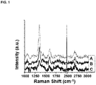
- Figure 1 includes the raw Raman spectra of samples A, B and C.
- the characteristic peaks of sp 2 bonding are observed in the Raman spectra: D peak centred at near 1350 cm -1 , G peak near 1580 cm -1 and 2D peak centred at 2700 cm -1 .
- the G peak shift from the standard position at 1580 cm -1 is really due to the appearance of the D' peak at 1620 cm -1 that merges in the G peak for small grain sizes.
- the spectrum of the sample A could be related to a monolayer or bilayer graphene film with small grain size, due to the similar intensities of the G and 2D peaks and quite high D peak.
- the intensity of the characteristic D peak, related to defects and grain boundaries, is quite strong in the case of samples B and C, sample C (high temperature) being the process with the smallest peak. This is a signature of enhanced grain size and quality.
- Another key difference is the intensity of the 2D peak in the spectrum of sample C, almost twice the G peak, and width, signature of monolayer graphene sheet. Higher 2D peak is a signature of enhanced quality and, in addition, in this sample C, the D peak is the smallest, in relation with grain boundaries.
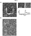
- Figures 2 , 3 , 4 and 5 show the corresponding AFM images of the samples.
- Figure 2A and 2B corresponds to sample A.
- the measure in figure 2A shows that the thickness is less than 1 nm, a typical value of monolayer graphene on the silica surface.
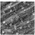
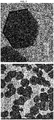
- Figures 3 and 4 show the AFM images of the samples B and C respectively. Both samples show enlarged grain size over 100 nm, and an order of magnitude larger than sample A.
- Figure 5 show the AFM image of the sample D with enlarged grain size over 200 nm on quartz.
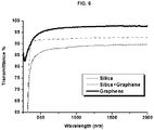
- Figure 6 shows the transmittance spectra of sample E.
- the substrate and substrate with graphene spectra have been obtained with a reference spectrum in air (for 100% transmittance reference).
- the graphene alone spectrum is measured by previously obtaining a reference spectrum of the substrate (for 100% transmittance reference).
- Figure 7 shows AFM images in friction of sample F. A grain size over 400 nm and being enlarged proportionally to the time of growth is observed. Enhanced nucleation and a crystal size of monolayer domains is observed.
- Figure 8 shows a diagram of a simple test to evaluate resistive thermal behaviour.
- the test was carried out on graphene films of sample E (3) onto the isolated silica substrate (4).
- the test consists of applying a voltage through two electrodes (1 and 2) to the surface of the sample on the side of the layer, and simultaneously measuring the temperature of the sample on the opposite side with the help of a thermocouple (5).
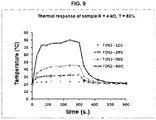
- Figure 9 shows the results of the measurements on sample E.
- the transmittance data relates to the glass-coating assembly.
Landscapes
- Chemical & Material Sciences (AREA)
- Engineering & Computer Science (AREA)
- Organic Chemistry (AREA)
- Materials Engineering (AREA)
- Life Sciences & Earth Sciences (AREA)
- Wood Science & Technology (AREA)
- Nanotechnology (AREA)
- Inorganic Chemistry (AREA)
- Physics & Mathematics (AREA)
- General Physics & Mathematics (AREA)
- Condensed Matter Physics & Semiconductors (AREA)
- Crystallography & Structural Chemistry (AREA)
- Chemical Kinetics & Catalysis (AREA)
- Mechanical Engineering (AREA)
- Metallurgy (AREA)
- Composite Materials (AREA)
- General Chemical & Material Sciences (AREA)
- Plasma & Fusion (AREA)
- Manufacturing & Machinery (AREA)
- Carbon And Carbon Compounds (AREA)
- Chemical Vapour Deposition (AREA)
Abstract
Description
- The invention relates to a deposition process of graphene layers onto a substrate being performed by plasma-assisted chemical vapour deposition, said graphene layers comprising nanocrystals of time and temperature controllable sizes interconnected by amorphous phase. Furthermore, the invention relates to said material deposited onto a substrate and its use as a component of windows or touch panels, protection systems, electrodes, as an element of hard-disk read heads/platters, as a resistant coating and as a component of a heater or a resistance heater.
- Graphene, the one atom thick layer of carbon, uniquely combines outstanding physical properties that justify its nickname of a "miracle material". A number of these properties -mechanical stiffness, strength, elasticity, electrical and thermal conductivity- are extreme. Moreover, the combination of these properties suggests that graphene could replace current materials in existing applications rapidly. This versatility could justify the common inconveniences of switching to a new technology in industrial processes. One example of this is the combination of transparency and conductivity that will find use, for example, in photovoltaic solar cells or flexible electronics as a cheap transparent electrode.
- The first isolation of graphene was performed in 2004 by using mechanical exfoliation of graphite, successively thinning the graphite sample. This fact astonished the scientific community because graphene was thought to be a theoretical material which could not exist, thermodynamically unstable and unable to withstand thermal fluctuations. Materials scientists were unaware of the existence of stable, isolated and freestanding 2D crystals. After this first demonstration, the mechanical exfoliation method allowed researchers worldwide to isolate graphene microlayers of suitable quality to demonstrate locally their outstanding physical properties. The main drawback of this method, however, was that only small area sheets with uncontrolled number of exfoliated layers could be produced.
- It is worth briefly mentioning that one key question regarding exfoliated graphene is its inherent high quality, related to the number of defects and degree of crystallinity. The quality of small "flakes" samples depends on the defect density and structural order of the precursor graphite. A typical precursor graphite of high purity and quality is highly oriented pyrolytic graphite (HOPG). This material is obtained from pyrolysis of organic compounds. Pyrolytic graphite, obtained by heat treatment of pyrolytic carbon or by Chemical Vapour Deposition (CVD) above 2500 K, exhibits a high degree of preferred crystallographic orientation perpendicular to the surface. Subsequent annealing under conditions of high compressive stress at approximately 3300 K results in HOPG. Thus, HOPG incorporates a low impurity level of the order of ppm and a lateral grain size typically of the order of mm. That's why exfoliated sheets exhibit local properties close to the theoretical limits; the sheets can be part of one grain and therefore, isolated single crystals.
- Simultaneously, other methods to produce large area graphene samples with suitable lateral size for applications have been developed and continue their development, such as SiC sublimation and chemical vapour deposition (CVD). For the SiC sublimation method, the major concerns are the high price of the SiC substrate and the high temperatures over 1300 °C used in the method. Moreover, the method is limited to its inherent substrate if there is no transference of the film to other surfaces. The other method is the "bottom up" growth by CVD. Currently, numerous examples of large area graphene synthesis by CVD can be found in the literature and the CVD of large area graphene layers has become a hot topic in material science and technology.
- The standard CVD processes are based on heterogeneous catalysis of organic precursors and performed on metal substrates at much lower temperature and pressure (less than 1350 K and 1 Atm), than those mentioned in HOPG and SiC. The crystallization mechanism is quite different in both cases. Bulk 3D pyrolytic graphite has a limited degree of crystallization if annealed at low temperature and pressure. Extreme thermodynamic conditions are essential for a large crystal size in bulk carbon materials. And extreme temperatures are essential in the evaporation of the SiC surface. As the goal in CVD of graphene is not a 3D, but a 2D material, the process of heterogeneous catalysis over transition metals has proven to be effective. The metal performs the two different roles of catalyst and substrate. It favours the decomposition of CVD carbon precursors at lower temperature, while 2D pure graphene layer is formed over the entire surface following the stages of "nucleation" of carbon radicals and continuous "growth".
- As a result of this mechanism, in the case of large area synthesis by CVD, graphene films exhibit a polycrystalline structure wherein the final film is a result of the coalescence of multiple domains. This process concludes when the metal is saturated or its surface is completely covered being quite similar to the "catalyst poisoning" in a typical catalytic process. Some reports have already appeared on the synthesis of millimetre-size single crystals by catalytic CVD, controlling the thermodynamics and kinetics of the nucleation and growth processes. Even wafer size single crystal graphene has been claimed recently.
- Catalytic CVD has some drawbacks at present. On one hand, the transference of the film to the desired substrate for usage normally induces wrinkles, contamination or even breakage because the underlying metal has to be chemically removed. On the other hand, large energy consumption at the typical synthesis temperature, and the temperature itself, make the process incompatible with current production technologies. Difficulties were also encountered when growing large area multilayer films on functional substrates. In this scenario, the game changing breakthrough would be the development of CVD processes to deposit high quality graphene layers on arbitrary substrates, at low temperature.
- In recent times, many approaches have been developed in an attempt to partially or fully solve these aspects. Parallel routes have been tested by many groups in this area that include low temperature synthesis on metals by plasma assisted CVD, direct synthesis on desired dielectric substrates, commonly at high temperature, without plasma technology and finally the combination of both, namely, direct synthesis on desired substrates at low temperature by means of plasma assisted deposition. Up to now, the main CVD technologies that have been used in graphene synthesis include, among others, radio frequency plasma enhanced CVD (RF-PECVD), microwave plasma CVD (MPCVD) and Electron Cyclotron Resonance CVD (ECR-CVD) [H. Medina, Y-C. Lin, C. Jin, C-C. Lu, C-H. Yeh, K-P. Huang, K. Suenaga, J. Robertson, P-W. Chiu, Adv. Func. Mater. 2012, 22, 2123].
- First, for low temperature synthesis on metals by plasma assisted techniques, high quality graphene has been grown by MPCVD on Cu foils at 700°C and between 450°C-750°C on Ni, the quality of these films being comparable to those grown by thermal CVD. Large area roll-to-roll approaches to grow graphene on Cu foils (294 mm wide) and Al foils at 300°C-400°C by surface wave plasma assisted CVD has been also performed using CH4/H2/Ar mixtures. Graphene films with few layer structure have been also deposited on Cu at temperatures as low as 240°C using a gas mixture of C2H2 and Ar by MPCVD. These films show smaller graphene domain sizes compared to graphene deposited by thermal CVD. Multilayer graphene has been also deposited by RF-PECVD at 500°C on Cu with acceptable qualities and on Ni at 650°C using traces of CH4. In all these examples post transfer process is needed. In this area of research two more approaches could be included. On the one hand, the synthesis at low temperature by using metal alloys acting as a catalyst. On the other hand, the use of Ni or Cu films at high synthesis temperatures over 1000°C which are subsequently evaporated, which effectively avoids the post-transfer processes. Although the evaporation of the catalyst is not complete in the case of Ni, the monolayer graphene exhibits optoelectronic properties that exceed the properties of transferred films.
- A second route involves direct synthesis on desired substrates normally at elevated temperatures and without plasma assistance. Atmospheric Pressure CVD (APCVD) synthesis of monolayer or few layer graphene has been performed on Si3N4 at 1000°C and 1150°C resulting in continuous films with dozens of nm sized domains and sheet resistance of 3 kΩ or less. Also, APCVD synthesis has been used on sapphire (Al2O3) between 1450°C and 1650°C with CH4 4as precursor with mobility over 2000 cm2/V·s for monolayer films- and at 950°C but with detrimental effects on electronic properties. Molecular beam epitaxy (MBE) from highly ordered pyrolytic graphite (HOPG) sublimation at 1100°C has also been tested on sapphire but the films presented small domain size, not usual at this temperature. There have also been published results of graphene grown by APCVD on SiO2 substrates at 1000°C with CH4 as precursor with sheet resistance around 5k Ω, and at 1100°C that show outstanding results with sheet resistances around 800 Ω and transmittance of 91% but in processes that take from 6 to 10 hours. Few layer graphene on h-BN flakes has also been deposited at 1000°C by APCVD. Synthesis of layered graphene flakes on MgO nanocrystal powder has been also carried out by low pressure CVD at temperatures between 325°C to 875C using acetylene and cyclohexane respectively, but optoelectronic properties have not been tested and Raman spectra of these samples exhibit the overlap of broadened G and D modes. In all these experiments the high temperatures limit the compatibility of these processes with microelectronic industrial processes.
- Combining both ideas implicit above, many groups have faced the challenge of direct synthesis of graphene films on desired substrates at low temperatures by means of plasma assisted deposition. Graphene flakes have been synthesized by MPCVD at 700°C on various dielectric substrates (quartz, SiO2). [A. Malesevic, R. Vitchev, K. Schouteden, A. Volodin, L. Zhang, G. Van Tendeloo, A. Vanhulsel, C. Van Haesendonck, Nanotech. 2008, 19, 305604]. Although Raman spectra have shown the high quality of the films, functional characterization has not been included. Remote PECVD has been also successfully applied in the direct synthesis of few layer nanographene type material at 550°C by using CH4 plasma on different dielectric substrates [L. Zhang, Z. Shi, Y. Wang, R. Yang, D. Shi, G. Zhang, Nano Res. 2011, 4(3), 315.] In this case the processes have taken a few hours and the best result on glass was a sheet resistance of 7 kΩ with transmittance of 85% and 40 kΩ on quartz with transmittance of 92%. Recently a much more rapid approach by using ECR-CVD has been published [H. Medina, Y-C. Lin, C. Jin, C-C. Lu, C-H. Yeh, K-P. Huang, K. Suenaga, J. Robertson, P-W. Chiu, Adv. Func. Mater. 2012, 22, 2123]. The authors ensure the synthesis of nanographene films on pure SiO2, glass and quartz at low temperature (400°C to 750°C) and in few minutes by using C2H4/Ar plasma. Although the exact synthesis temperature is not defined in each case, the published results of nanographene films on quartz exhibit outstanding transmittance from 94% to 82% and sheet resistances from 20 kΩ to 7 kΩ. Graphene films have been also produced by using a critical PECVD (c-PECVD) growth method, in which a H2 plasma has been introduced during graphene growth, in a critical equilibrium state between H2 plasma etching and CH4 or C2H4 plasma growth [Dacheng Wei, Yunhao Lu, Cheng Han, Tianchao Niu, Wei Chen, y Andrew Thye Shen Wee, Angew. Chem. Int. Ed. 2013, 52, 14121] [Donghua Liu, Wei Yang, Lianchang Zhang, Jing Zhang, Jianling Meng, Rong Yang, Guangyu Zhang, Dongxia Shi, Carbon. 2014, 72, 387.] These two methods have some drawbacks. In one case, the substrate has suffered a precleaning and annealing step at 1000°C, as in the case of the synthesis on metals. In the second case the Raman spectra show the low quality of the nanographene with a secondary fine structure inside the graphene flakes and poor electronic properties. Moreover, two or three synthesis steps are needed in both cases and crystalline or semiconducting substrates have been used.
- Finally, there have been many developments including PECVD or molecular beam epitaxy (MBE) techniques and epitaxial or heteroepitaxial growth at low temperatures but those approaches are limited to monocrystalline surfaces [
US 2014/0273414 A1 ,CN102910614 A ] - The invention relates to a deposition process of graphene layers onto a substrate being performed by plasma-assisted chemical vapour deposition. The main advantages of the invention are:
- Controllable size of the graphene nanocrystals.
- Time dependent and temperature dependent size of the graphene nanocrystals.
- Enhanced quality of the transparent and conducting graphene layers.
- Low temperature process compared to catalytic processes.
- Direct growth. Transference of the graphene film is avoided.
- Negligible amount of impurities, in relation with the gases used during the synthesis.
- The resulting material thereof is ready to include functionalisation by chemicals or to be decorated with nanostructures.
- It has been demonstrated that the resulting material reaches a medium conductivity of 900 Ohm/m, keeping high transparency (over 92%). With the relevant modifications to the steps of the method, a person skilled in the art could reach a medium conductivity (∼4 kOhm/m) in continuous films, keeping high transparency (over 95%).
- Furthermore, the invention relates to the material deposited onto a substrate, said material comprising at least a graphene layer and said graphene layer comprising nanocrystals interconnected by amorphous phase and its use.
- A first aspect of the present invention relates to a process of obtainment of a material deposited onto a substrate being performed by plasma-assisted chemical vapour deposition (herein the process of the invention), said material comprising
- At least a graphene layer and said graphene layer comprising nanocrystals interconnected by amorphous phase;
- a) placing the substrate into a vacuum chamber previously set at a pressure lower than 10-4 mbar and under an atmosphere of argon and hydrogen;
- b) setting the substrate of step a) to a first substrate temperature T1, wherein T1 reaches values between 400°C and 700°C;
- c) activating the plasma and adding a carbon source into the vacuum chamber for a time t1, wherein t1 reaches different values of less than 60 min, obtaining a sample formed by the substrate and the deposited material precursor;
- d) setting the sample obtained in step c) to a second substrate temperature T2, wherein T2 is T1 minus T3 wherein T3 reaches values between 30°C and 100°C for a time t2 wherein t2 is higher than t1, and
- e) deactivating the plasma and cooling the sample obtained in step d).
- The substrate of step a) should be stable at a temperature of 700°C. In a preferred embodiment, the substrate is selected from the list consisting of quartz, boron nitride, silicon carbide and sapphire. Even commercial glass substrates with finite roughness are feasible.
- The term "plasma" of step c) refers herein to conventional plasma sources, such as radiofrequency RF-CVD (13.56 MHz) activation, microwave MW-CVD (2.41 GHz) activation and Electron Cyclotron Resonance ECR-CVD (2.41 GHz) activation. Other plasma sources or technologies are feasible.
- Preferably, the plasma is an ECR-CVD plasma. The advantage of this source is the higher electron density, the higher ionization degree besides the larger efficiency in the dissociation of H2, that is, enhanced atomic H activation at low power.
- In another preferred embodiment of the invention, the carbon source of step c) is selected from the list consisting of methane CH4, acetylene C2H2, ethylene C2H4 and a combination thereof. The sample obtained in step c) is formed by the substrate and a deposited material precursor comprising graphene nanodomains nucleated on the surface of the substrate with a controlled and minimized nucleation density and controllable area, nanometric in size.
- In a more preferred embodiment of the invention, the nanocrystals forming the graphene layers have sizes between 10 nm and 400 nm. In a more preferred embodiment of the invention, the nanocrystals forming the graphene layers have sizes between 10 nm and 300 nm.
- In another preferred embodiment of the present invention, the step (e) is carried out under an atmosphere of hydrogen and/or argon.
- In another preferred embodiment of the present invention, the step (e) is carried out in a vacuum chamber.
- A second aspect of the present invention relates to a material deposited onto a substrate (herein the product of the invention) obtained by the process invention, wherein said material comprises
- at least a graphene layer,
- and said graphene layer comprising nanocrystals interconnected by amorphous phase.
- The term "time- and temperature-controllable sizes" refers herein to the size of the graphene nanocrystals reached when the substrate temperatures T1 is set during a time t1 and the T2 is set during a time t2. At higher T1, the thickness is easily controlled to give monolayer films as a result. When T1 and partial pressures are established, the higher t1 is, the higher the nucleation density. This step controls the number of nuclei per unit area. After nucleation, T2 is established to "edge growth", in the critical limit of nucleation and etching. If the selection is optimal, during t2, enlargement of the size of the nuclei is performed. The higher t2 is, the higher the nanocrystal size. As mentioned before, nanocrystals of sizes between 10 nm and 300 nm are obtained performing the process of the invention.
- The third aspect of the invention refers to the use of the product of the invention as a component of a window or a touch panel. Examples of windows are smart windows, defrosting windows, low-emissivity windows and oven windows.
- Another aspect of the invention refers to the use of the product of the invention as a component of a protection system such as an electromagnetic shielding.
- A further aspect of the invention relates to the use of the product of the invention as a component of electrodes in lithium batteries, fuel cells or sensors.
- Another aspect of the invention relates to the use of the product of the invention as a component of a hard-disk reader or a hard-disk platter.
- The following aspect of the invention relates to the use of the product of the invention as corrosion resistant coating for metals and stainless-steel substrates as in bipolar plates in fuel cells [Siva Böhm, Nat. Nanotech. 2014, 9, 741].
- The final aspect of the invention relates to the use of the product of the invention as a component of a heater or a resistance heater, preferably forming part of a transparent glass or quartz that is used in a transparent heater or resistance heater. Examples of these transparent heaters or resistance heaters are plates or dishware, thermal lunettes, heated thermal windows, etc.
- Unless otherwise defined, all technical and scientific terms used herein have the same meaning as commonly understood by a person with ordinary skill in the art to which this invention belongs. Methods and materials similar or equivalent to those described herein can be used in the practice of the present invention. Throughout the description and claims the word "comprise" and its variations are not intended to exclude other technical features, additives, components, or steps. Additional objects, advantages and features of the invention will become apparent to those skilled in the art upon examination of the description or may be learned by practice of the invention. The following examples and drawings are provided by way of illustration and are not intended to be limiting of the present invention.
-
-
FIG.1 . Raw Raman spectra of samples A, B, C. Spectrum C shows monolayer graphene on fused silica. -
FIG.2 . AFM image of sample A. A) Thickness measurement. The profile shows that the sample thickness is under 1 nm, signature of monolayer graphene. B) morphology of the sample surface. -
FIG.3 . AFM image of the morphology of the sample B. The image shows the enhanced grain size and the controlled nucleation density. -
FIG.4 . AFM image of sample C. Enhanced nucleation and grain size of monolayer domains. -
FIG.5 . AFM image of sample D, graphene on quartz. Enhanced nucleation and grain size of monolayer domains. -
FIG.6 . Transmittance spectra of sample E. Spectrum of graphene layer in black, obtained without the silica substrate contribution. -
FIG. 7 . AFM image of sample F in friction, graphene on quartz. -
FIG. 8 . Diagram of a thermal test. (1) Positive electrode (2) Negative electrode (3) Graphene (4) Silica and (5) Thermocouple. -
FIG. 9 . Thermal response of sample E with R = kΩ and transmittance greater than 83%. - The present invention provides a method for the direct manufacturing of graphene films on arbitrary substrates, including dielectric, metallic and semiconducting surfaces. The manufacturing process is easily scalable, and the graphene film is prepared by using electron cyclotron resonance plasma-assisted chemical vapour deposition at moderate substrate temperature (≤ 700°C) during the whole process, without using metal catalyst. This method avoids damaging and expensive transfer processes of graphene films and improves compatibility with current manufacturing technologies. Graphene films have been grown in a remote electron cyclotron resonance chemical vapour deposition r-(ECR-CVD) system using Ar to activate and stabilize the ECR plasma, H2 as a diluent and stabiliser (etching agent) of graphitic material and CH4 - C2H2 as carbon precursor. The system mainly consists of a microwave power source, a two-zone chamber and a two-stage pumping system.
- Table 1 describes the experimental conditions used for obtaining graphene films. These profiles are based on the variation of the partial pressures of the precursors (changing the atmosphere) and/or the temperature to obtain the graphene layer with controllable (within a certain range) grain size and number of layers.
- All experiments have been performed on fused silica and quartz substrates.
Table 1: Description of the experimental conditions for obtaining samples A, B, C, D, E and F. Deposition profiles of samples. SAMPLE A B C D E F POWER (W) 40 100 100 100 100 100 SUBSTRATE fused silica fused silica fused silica quartz fused silica quartz GASES Ar/H2/C2H2 H2/C2H2 H2/C2H2 H2/C2H2 H2/C2H2 H2/C2H2 PRESSURE (mbar) 1.2·10-1 3·10-2 3·10-2 5.4·10-2 3·10-2 5.4·10-2 T1 (°C) 700 625 675 700 675 670 t1 (min) 180 4 4 4 2 20 T2 (°C) --- 575 625 650 625 660 t2 (min) --- 180 90 240 210 480 AFM image Fig 2 A2B Fig 3 Fig 4 Fig 5 --- Fig 7 Raman Spectrum A B C --- --- --- Transmittance --- --- --- --- Fig 6 --- Sheet Resistance --- --- --- --- ∼4 kOhm --- - By using remote plasma activation, the detrimental effects of the plasma ion etching on the quality of the films are avoided. The effective activation of carbon species (C2H2, CH4) and the etching agent (H2, H) in the plasma was followed by optical emission spectroscopy (OES). The nanostructure and the crystallinity of the films have been characterized by Atomic Force Microscopy (AFM) and Raman spectroscopy. The continuity, transmittance and sheet resistance have been characterized by UV-Vis-NIR spectrophotometry and point probe measurements. The process is reproducible and compatible with current optoelectronic manufacturing technologies.
- Fundamental characterization of the structure of the samples A, B, C, D, E and F has been carried out by means of Raman spectroscopy (ENWAVE Optronics EZRaman-N) and AFM microscopy (NANOTEC Electronics Dulcinea Control System). The performance of the E has been characterized by means of UV-Vis-NIR spectrophotometry (SHIMADZU SolidSpec - 3700 Spectrophotometer) for transmittance and four point probe measurement (JANDEL RMS2 Universal Probe) with continuous current (from 1 µA -100 µA).
-
Figure 1 includes the raw Raman spectra of samples A, B and C. - For all the samples, the characteristic peaks of sp2 bonding are observed in the Raman spectra: D peak centred at near 1350 cm-1, G peak near 1580 cm-1 and 2D peak centred at 2700 cm-1. The G peak shift from the standard position at 1580 cm-1 is really due to the appearance of the D' peak at 1620 cm-1 that merges in the G peak for small grain sizes.
- There are clear differences observed among the spectra. The spectrum of the sample A could be related to a monolayer or bilayer graphene film with small grain size, due to the similar intensities of the G and 2D peaks and quite high D peak. The intensity of the characteristic D peak, related to defects and grain boundaries, is quite strong in the case of samples B and C, sample C (high temperature) being the process with the smallest peak. This is a signature of enhanced grain size and quality. Another key difference is the intensity of the 2D peak in the spectrum of sample C, almost twice the G peak, and width, signature of monolayer graphene sheet. Higher 2D peak is a signature of enhanced quality and, in addition, in this sample C, the D peak is the smallest, in relation with grain boundaries.
-
Figures 2 ,3 ,4 and5 show the corresponding AFM images of the samples.Figure 2A and 2B corresponds to sample A. The measure infigure 2A shows that the thickness is less than 1 nm, a typical value of monolayer graphene on the silica surface.Figures 3 and4 show the AFM images of the samples B and C respectively. Both samples show enlarged grain size over 100 nm, and an order of magnitude larger than sample A.Figure 5 show the AFM image of the sample D with enlarged grain size over 200 nm on quartz. -
Figure 6 shows the transmittance spectra of sample E. We include the transmittance spectra of the substrate alone, the substrate with graphene and the graphene alone. The substrate and substrate with graphene spectra have been obtained with a reference spectrum in air (for 100% transmittance reference). The graphene alone spectrum is measured by previously obtaining a reference spectrum of the substrate (for 100% transmittance reference). -
Figure 7 shows AFM images in friction of sample F. A grain size over 400 nm and being enlarged proportionally to the time of growth is observed. Enhanced nucleation and a crystal size of monolayer domains is observed. -
Figure 8 shows a diagram of a simple test to evaluate resistive thermal behaviour. The test was carried out on graphene films of sample E (3) onto the isolated silica substrate (4). The test consists of applying a voltage through two electrodes (1 and 2) to the surface of the sample on the side of the layer, and simultaneously measuring the temperature of the sample on the opposite side with the help of a thermocouple (5). -
Figure 9 shows the results of the measurements on sample E. The transmittance data relates to the glass-coating assembly. Four tests at different power supplies, 12 V, 24 V, 36 V and 60 V, were carried out. The measurements were taken until reaching equilibrium, and the test lasted approximately 5 minutes. At the end of this time, the power (OFF) was disconnected and it was left to cool freely. It is observed that the glass has very quick heating and cooling rates, reaching the maximum in about 60 seconds. A proportionality between the voltage applied and the temperature reaches is also observed.
Claims (15)
- A process of obtainment of a material deposited onto a substrate being performed by plasma-assisted chemical vapour deposition, said material comprising• at least a graphene layer and said graphene layer comprising nanocrystals interconnected by amorphous phase;• and said process characterised in that it comprises the following steps:a) placing the substrate into a vacuum chamber previously set at a pressure lower than 10-4 mbar and under an atmosphere of argon and hydrogen;b) setting the substrate of step a) to a first substrate temperature T1, wherein T1 reaches values between 400°C and 700°C;c) activating the plasma and adding a carbon source into the vacuum chamber for a time t1, wherein t1 reaches different values of less than 60 min, obtaining a sample formed by the substrate and the deposited material precursor;d) setting the sample obtained in step c) to a second substrate temperature T2, wherein T2 is T1 minus T3 wherein T3 reaches values between 30°C and 100°C for a time t2 wherein t2 is higher than t1, ande) deactivating the plasma and cooling the sample obtained in step d).
- The process according to the preceding claim, wherein the substrate of step a) is selected from the list consisting of fused silica, silicon carbide, quartz, boron nitride and sapphire.
- The process according to any of claims 1 or 2, wherein the plasma of step c) is an electron cyclotron resonance plasma.
- The process according to any of claims 1 to 3, wherein the carbon source of step c) is selected from the list consisting of methane, acetylene, ethylene and a combination thereof.
- The process according to any of claims 1 to 4, wherein the nanocrystals forming the graphene layers have sizes between 10 nm and 400 nm.
- The process according to claims 5, wherein the nanocrystals forming the graphene layers have sizes between 10 nm and 300 nm.
- The process according to any of claims 1 to 6, wherein step e) is carried out under an atmosphere of hydrogen and/or argon.
- The process according to any of claims 1 to 6, wherein step e) is carried out in a vacuum chamber.
- A material deposited onto a substrate obtained by the process according to any of claims 1 to 8, wherein said material comprises at least a graphene layer, and said graphene layer comprising nanocrystals interconnected by amorphous phase.
- Use of the material according to claim 9 as a component of a window or a touch panel.
- Use of the material according to claim 9 as a component of a protection system.
- Use of the material according to claim 9 as a component of electrodes in lithium batteries, fuel cells or sensors.
- Use of the material according to claim 9 as a component of a hard-disk reader or a hard-disk platter.
- Use of the material according to claim 9 as corrosion resistance coating for metals and stainless-steel substrates.
- Use of the material according to claim 9 as a component of a heater or a resistance heater.
Applications Claiming Priority (2)
| Application Number | Priority Date | Filing Date | Title |
|---|---|---|---|
| ES201530864A ES2597477A1 (en) | 2015-06-18 | 2015-06-18 | DEPOSITION OF GRAPHENE LAYERS THROUGH CHEMICAL DEPOSITION IN THE VAPOR PHASE ASSISTED BY PLASMA |
| PCT/ES2016/070451 WO2016203083A1 (en) | 2015-06-18 | 2016-06-15 | Deposition of graphene layers by means of plasma-enhanced chemical vapour deposition |
Publications (3)
| Publication Number | Publication Date |
|---|---|
| EP3312137A1 true EP3312137A1 (en) | 2018-04-25 |
| EP3312137A4 EP3312137A4 (en) | 2019-02-27 |
| EP3312137B1 EP3312137B1 (en) | 2021-02-24 |
Family
ID=57546322
Family Applications (1)
| Application Number | Title | Priority Date | Filing Date |
|---|---|---|---|
| EP16811071.6A Not-in-force EP3312137B1 (en) | 2015-06-18 | 2016-06-15 | Deposition of graphene layers by means of plasma-enhanced chemical vapour deposition |
Country Status (3)
| Country | Link |
|---|---|
| EP (1) | EP3312137B1 (en) |
| ES (1) | ES2597477A1 (en) |
| WO (1) | WO2016203083A1 (en) |
Cited By (2)
| Publication number | Priority date | Publication date | Assignee | Title |
|---|---|---|---|---|
| CN113998666A (en) * | 2021-10-21 | 2022-02-01 | 北京理工大学 | High-sensitivity full-graphene artificial electronic skin capable of resisting ultra-large strain |
| CN116002672A (en) * | 2022-11-28 | 2023-04-25 | 季华实验室 | Graphene crystal preparation method |
Families Citing this family (7)
| Publication number | Priority date | Publication date | Assignee | Title |
|---|---|---|---|---|
| KR102592698B1 (en) * | 2017-11-29 | 2023-10-24 | 삼성전자주식회사 | Nanocrystalline graphene and method for forming nanocrystalline graphene |
| KR102233953B1 (en) * | 2018-06-28 | 2021-03-30 | 박미영 | Electrode for structural batteries, manufacturing method of the electrode, and structural batteries using the electrode |
| CN111170304A (en) * | 2018-11-13 | 2020-05-19 | 广州墨羲科技有限公司 | Three-dimensional carbon nanosheet electrode additive and preparation method thereof |
| CN109461594B (en) * | 2018-12-25 | 2023-02-28 | 重庆中科超容科技有限公司 | High-voltage-resistance doped three-dimensional porous graphene/activated carbon electrode material and preparation method thereof |
| CN111517307B (en) * | 2019-02-01 | 2022-11-22 | 中国科学院金属研究所 | Method for growing single-layer graphene on nonmetal substrate by rapid CVD |
| CN110817852B (en) * | 2019-12-18 | 2021-04-20 | 北京石墨烯研究院 | Graphene preparation method based on water treatment-assisted mechanism |
| CN115313903A (en) * | 2022-08-02 | 2022-11-08 | 浙江大学 | Friction nanometer generator based on vertical graphene array and preparation method thereof |
Family Cites Families (4)
| Publication number | Priority date | Publication date | Assignee | Title |
|---|---|---|---|---|
| WO2011025045A1 (en) * | 2009-08-31 | 2011-03-03 | 独立行政法人科学技術振興機構 | Graphene film and method for producing same |
| TWI434949B (en) * | 2012-03-14 | 2014-04-21 | Nat Univ Tsing Hua | Chemical vapor deposition of graphene on dielectrics |
| CN107419236B (en) * | 2013-01-14 | 2019-07-12 | 加州理工学院 | Methods and systems for graphene formation |
| WO2014112953A1 (en) * | 2013-01-18 | 2014-07-24 | Nanyang Technological University | Methods of low temperature preparation of one or more layers of graphene on a metallic substrate for anti-corrosion and anti-oxidation applications |
-
2015
- 2015-06-18 ES ES201530864A patent/ES2597477A1/en active Granted
-
2016
- 2016-06-15 EP EP16811071.6A patent/EP3312137B1/en not_active Not-in-force
- 2016-06-15 WO PCT/ES2016/070451 patent/WO2016203083A1/en not_active Ceased
Cited By (2)
| Publication number | Priority date | Publication date | Assignee | Title |
|---|---|---|---|---|
| CN113998666A (en) * | 2021-10-21 | 2022-02-01 | 北京理工大学 | High-sensitivity full-graphene artificial electronic skin capable of resisting ultra-large strain |
| CN116002672A (en) * | 2022-11-28 | 2023-04-25 | 季华实验室 | Graphene crystal preparation method |
Also Published As
| Publication number | Publication date |
|---|---|
| WO2016203083A1 (en) | 2016-12-22 |
| EP3312137B1 (en) | 2021-02-24 |
| EP3312137A4 (en) | 2019-02-27 |
| ES2597477A1 (en) | 2017-01-18 |
Similar Documents
| Publication | Publication Date | Title |
|---|---|---|
| EP3312137B1 (en) | Deposition of graphene layers by means of plasma-enhanced chemical vapour deposition | |
| EP2851457B1 (en) | Method for manufacturing a single crystal diamond | |
| US11124870B2 (en) | Transfer-free method for producing graphene thin film | |
| CN102260858B (en) | Method for directly growing graphine on various substrates | |
| US8859044B2 (en) | Method of preparing graphene layer | |
| Huet et al. | Pressure-controlled chemical vapor deposition of single-layer graphene with millimeter-size domains on thin copper film | |
| EP2850032A1 (en) | Methods of growing uniform, large-scale, multilayer graphene films | |
| JP2009062247A (en) | Graphene sheet manufacturing method | |
| US9371582B2 (en) | Method for manufacturing silicon carbide thin film | |
| KR20130001253A (en) | Carbon film laminate | |
| CN110699749B (en) | A kind of method for preparing large-area continuous single-layer single-crystal graphene film | |
| EP1832673A1 (en) | Method for producing substrate for single crystal diamond growth | |
| US20240166521A1 (en) | A method of forming a graphene layer structure and a graphene substrate | |
| WO2016149934A1 (en) | Growing method for graphene | |
| KR101877500B1 (en) | Method for in-situ Preparation of Graphene Thin Film | |
| JP4528654B2 (en) | Multilayer substrate, method for manufacturing multilayer substrate, and device | |
| CN104909359A (en) | A Direct and Rapid Preparation of Single-layer Graphene on SiO2/Si Substrate | |
| CN104404620B (en) | Method for simultaneously growing graphene on silicon surface and carbon surface of large-diameter 6H/4H-SiC | |
| CN110228806A (en) | The method for preparing graphene film using plasma reinforced chemical vapour deposition method | |
| Hu et al. | Effects of substrate and transfer on CVD-grown graphene over sapphire-induced Cu films | |
| US20140193574A1 (en) | Graphene manufacturing system and the method thereof | |
| TW202339947A (en) | Composite substrate, laminated body, manufacturing method of composite substrate, manufacturing method of laminated body | |
| CN103060907B (en) | A kind of method preparing single crystal graphene on the insulating material | |
| KR101484770B1 (en) | Method for preparing graphene using cover and method for fabricating electronic device comprising the same | |
| CN111139526A (en) | A method for obtaining single crystal boron nitride thin film by ion beam sputtering deposition |
Legal Events
| Date | Code | Title | Description |
|---|---|---|---|
| STAA | Information on the status of an ep patent application or granted ep patent |
Free format text: STATUS: THE INTERNATIONAL PUBLICATION HAS BEEN MADE |
|
| PUAI | Public reference made under article 153(3) epc to a published international application that has entered the european phase |
Free format text: ORIGINAL CODE: 0009012 |
|
| STAA | Information on the status of an ep patent application or granted ep patent |
Free format text: STATUS: REQUEST FOR EXAMINATION WAS MADE |
|
| 17P | Request for examination filed |
Effective date: 20180117 |
|
| AK | Designated contracting states |
Kind code of ref document: A1 Designated state(s): AL AT BE BG CH CY CZ DE DK EE ES FI FR GB GR HR HU IE IS IT LI LT LU LV MC MK MT NL NO PL PT RO RS SE SI SK SM TR |
|
| AX | Request for extension of the european patent |
Extension state: BA ME |
|
| DAV | Request for validation of the european patent (deleted) | ||
| DAX | Request for extension of the european patent (deleted) | ||
| A4 | Supplementary search report drawn up and despatched |
Effective date: 20190128 |
|
| RIC1 | Information provided on ipc code assigned before grant |
Ipc: C01B 32/05 20170101ALI20190122BHEP Ipc: C09D 1/00 20060101ALI20190122BHEP Ipc: B82Y 30/00 20110101ALI20190122BHEP Ipc: C23C 16/50 20060101ALI20190122BHEP Ipc: B82Y 40/00 20110101AFI20190122BHEP |
|
| GRAP | Despatch of communication of intention to grant a patent |
Free format text: ORIGINAL CODE: EPIDOSNIGR1 |
|
| STAA | Information on the status of an ep patent application or granted ep patent |
Free format text: STATUS: GRANT OF PATENT IS INTENDED |
|
| RIC1 | Information provided on ipc code assigned before grant |
Ipc: B82Y 30/00 20110101ALI20200917BHEP Ipc: C09D 5/08 20060101ALI20200917BHEP Ipc: B82Y 40/00 20110101AFI20200917BHEP Ipc: C09D 7/61 20180101ALI20200917BHEP Ipc: C09D 1/00 20060101ALI20200917BHEP Ipc: C23C 16/50 20060101ALI20200917BHEP Ipc: C09D 7/40 20180101ALI20200917BHEP Ipc: C01B 32/05 20170101ALI20200917BHEP |
|
| INTG | Intention to grant announced |
Effective date: 20201009 |
|
| GRAS | Grant fee paid |
Free format text: ORIGINAL CODE: EPIDOSNIGR3 |
|
| GRAA | (expected) grant |
Free format text: ORIGINAL CODE: 0009210 |
|
| STAA | Information on the status of an ep patent application or granted ep patent |
Free format text: STATUS: THE PATENT HAS BEEN GRANTED |
|
| AK | Designated contracting states |
Kind code of ref document: B1 Designated state(s): AL AT BE BG CH CY CZ DE DK EE ES FI FR GB GR HR HU IE IS IT LI LT LU LV MC MK MT NL NO PL PT RO RS SE SI SK SM TR |
|
| REG | Reference to a national code |
Ref country code: CH Ref legal event code: EP |
|
| REG | Reference to a national code |
Ref country code: AT Ref legal event code: REF Ref document number: 1364216 Country of ref document: AT Kind code of ref document: T Effective date: 20210315 |
|
| REG | Reference to a national code |
Ref country code: IE Ref legal event code: FG4D |
|
| REG | Reference to a national code |
Ref country code: DE Ref legal event code: R096 Ref document number: 602016053230 Country of ref document: DE |
|
| REG | Reference to a national code |
Ref country code: LT Ref legal event code: MG9D |
|
| REG | Reference to a national code |
Ref country code: NL Ref legal event code: MP Effective date: 20210224 |
|
| PG25 | Lapsed in a contracting state [announced via postgrant information from national office to epo] |
Ref country code: HR Free format text: LAPSE BECAUSE OF FAILURE TO SUBMIT A TRANSLATION OF THE DESCRIPTION OR TO PAY THE FEE WITHIN THE PRESCRIBED TIME-LIMIT Effective date: 20210224 Ref country code: FI Free format text: LAPSE BECAUSE OF FAILURE TO SUBMIT A TRANSLATION OF THE DESCRIPTION OR TO PAY THE FEE WITHIN THE PRESCRIBED TIME-LIMIT Effective date: 20210224 Ref country code: GR Free format text: LAPSE BECAUSE OF FAILURE TO SUBMIT A TRANSLATION OF THE DESCRIPTION OR TO PAY THE FEE WITHIN THE PRESCRIBED TIME-LIMIT Effective date: 20210525 Ref country code: PT Free format text: LAPSE BECAUSE OF FAILURE TO SUBMIT A TRANSLATION OF THE DESCRIPTION OR TO PAY THE FEE WITHIN THE PRESCRIBED TIME-LIMIT Effective date: 20210624 Ref country code: NO Free format text: LAPSE BECAUSE OF FAILURE TO SUBMIT A TRANSLATION OF THE DESCRIPTION OR TO PAY THE FEE WITHIN THE PRESCRIBED TIME-LIMIT Effective date: 20210524 Ref country code: LT Free format text: LAPSE BECAUSE OF FAILURE TO SUBMIT A TRANSLATION OF THE DESCRIPTION OR TO PAY THE FEE WITHIN THE PRESCRIBED TIME-LIMIT Effective date: 20210224 Ref country code: BG Free format text: LAPSE BECAUSE OF FAILURE TO SUBMIT A TRANSLATION OF THE DESCRIPTION OR TO PAY THE FEE WITHIN THE PRESCRIBED TIME-LIMIT Effective date: 20210524 |
|
| REG | Reference to a national code |
Ref country code: AT Ref legal event code: MK05 Ref document number: 1364216 Country of ref document: AT Kind code of ref document: T Effective date: 20210224 |
|
| PG25 | Lapsed in a contracting state [announced via postgrant information from national office to epo] |
Ref country code: LV Free format text: LAPSE BECAUSE OF FAILURE TO SUBMIT A TRANSLATION OF THE DESCRIPTION OR TO PAY THE FEE WITHIN THE PRESCRIBED TIME-LIMIT Effective date: 20210224 Ref country code: RS Free format text: LAPSE BECAUSE OF FAILURE TO SUBMIT A TRANSLATION OF THE DESCRIPTION OR TO PAY THE FEE WITHIN THE PRESCRIBED TIME-LIMIT Effective date: 20210224 Ref country code: PL Free format text: LAPSE BECAUSE OF FAILURE TO SUBMIT A TRANSLATION OF THE DESCRIPTION OR TO PAY THE FEE WITHIN THE PRESCRIBED TIME-LIMIT Effective date: 20210224 Ref country code: NL Free format text: LAPSE BECAUSE OF FAILURE TO SUBMIT A TRANSLATION OF THE DESCRIPTION OR TO PAY THE FEE WITHIN THE PRESCRIBED TIME-LIMIT Effective date: 20210224 Ref country code: SE Free format text: LAPSE BECAUSE OF FAILURE TO SUBMIT A TRANSLATION OF THE DESCRIPTION OR TO PAY THE FEE WITHIN THE PRESCRIBED TIME-LIMIT Effective date: 20210224 |
|
| PG25 | Lapsed in a contracting state [announced via postgrant information from national office to epo] |
Ref country code: IS Free format text: LAPSE BECAUSE OF FAILURE TO SUBMIT A TRANSLATION OF THE DESCRIPTION OR TO PAY THE FEE WITHIN THE PRESCRIBED TIME-LIMIT Effective date: 20210624 |
|
| PG25 | Lapsed in a contracting state [announced via postgrant information from national office to epo] |
Ref country code: SM Free format text: LAPSE BECAUSE OF FAILURE TO SUBMIT A TRANSLATION OF THE DESCRIPTION OR TO PAY THE FEE WITHIN THE PRESCRIBED TIME-LIMIT Effective date: 20210224 Ref country code: AT Free format text: LAPSE BECAUSE OF FAILURE TO SUBMIT A TRANSLATION OF THE DESCRIPTION OR TO PAY THE FEE WITHIN THE PRESCRIBED TIME-LIMIT Effective date: 20210224 Ref country code: CZ Free format text: LAPSE BECAUSE OF FAILURE TO SUBMIT A TRANSLATION OF THE DESCRIPTION OR TO PAY THE FEE WITHIN THE PRESCRIBED TIME-LIMIT Effective date: 20210224 Ref country code: EE Free format text: LAPSE BECAUSE OF FAILURE TO SUBMIT A TRANSLATION OF THE DESCRIPTION OR TO PAY THE FEE WITHIN THE PRESCRIBED TIME-LIMIT Effective date: 20210224 |
|
| REG | Reference to a national code |
Ref country code: DE Ref legal event code: R097 Ref document number: 602016053230 Country of ref document: DE |
|
| PG25 | Lapsed in a contracting state [announced via postgrant information from national office to epo] |
Ref country code: DK Free format text: LAPSE BECAUSE OF FAILURE TO SUBMIT A TRANSLATION OF THE DESCRIPTION OR TO PAY THE FEE WITHIN THE PRESCRIBED TIME-LIMIT Effective date: 20210224 Ref country code: SK Free format text: LAPSE BECAUSE OF FAILURE TO SUBMIT A TRANSLATION OF THE DESCRIPTION OR TO PAY THE FEE WITHIN THE PRESCRIBED TIME-LIMIT Effective date: 20210224 Ref country code: RO Free format text: LAPSE BECAUSE OF FAILURE TO SUBMIT A TRANSLATION OF THE DESCRIPTION OR TO PAY THE FEE WITHIN THE PRESCRIBED TIME-LIMIT Effective date: 20210224 |
|
| PLBE | No opposition filed within time limit |
Free format text: ORIGINAL CODE: 0009261 |
|
| STAA | Information on the status of an ep patent application or granted ep patent |
Free format text: STATUS: NO OPPOSITION FILED WITHIN TIME LIMIT |
|
| REG | Reference to a national code |
Ref country code: DE Ref legal event code: R119 Ref document number: 602016053230 Country of ref document: DE |
|
| PG25 | Lapsed in a contracting state [announced via postgrant information from national office to epo] |
Ref country code: ES Free format text: LAPSE BECAUSE OF FAILURE TO SUBMIT A TRANSLATION OF THE DESCRIPTION OR TO PAY THE FEE WITHIN THE PRESCRIBED TIME-LIMIT Effective date: 20210224 Ref country code: AL Free format text: LAPSE BECAUSE OF FAILURE TO SUBMIT A TRANSLATION OF THE DESCRIPTION OR TO PAY THE FEE WITHIN THE PRESCRIBED TIME-LIMIT Effective date: 20210224 Ref country code: MC Free format text: LAPSE BECAUSE OF FAILURE TO SUBMIT A TRANSLATION OF THE DESCRIPTION OR TO PAY THE FEE WITHIN THE PRESCRIBED TIME-LIMIT Effective date: 20210224 |
|
| REG | Reference to a national code |
Ref country code: CH Ref legal event code: PL |
|
| 26N | No opposition filed |
Effective date: 20211125 |
|
| GBPC | Gb: european patent ceased through non-payment of renewal fee |
Effective date: 20210615 |
|
| PG25 | Lapsed in a contracting state [announced via postgrant information from national office to epo] |
Ref country code: SI Free format text: LAPSE BECAUSE OF FAILURE TO SUBMIT A TRANSLATION OF THE DESCRIPTION OR TO PAY THE FEE WITHIN THE PRESCRIBED TIME-LIMIT Effective date: 20210224 |
|
| REG | Reference to a national code |
Ref country code: BE Ref legal event code: MM Effective date: 20210630 |
|
| PG25 | Lapsed in a contracting state [announced via postgrant information from national office to epo] |
Ref country code: LU Free format text: LAPSE BECAUSE OF NON-PAYMENT OF DUE FEES Effective date: 20210615 |
|
| PG25 | Lapsed in a contracting state [announced via postgrant information from national office to epo] |
Ref country code: LI Free format text: LAPSE BECAUSE OF NON-PAYMENT OF DUE FEES Effective date: 20210630 Ref country code: IT Free format text: LAPSE BECAUSE OF FAILURE TO SUBMIT A TRANSLATION OF THE DESCRIPTION OR TO PAY THE FEE WITHIN THE PRESCRIBED TIME-LIMIT Effective date: 20210224 Ref country code: IE Free format text: LAPSE BECAUSE OF NON-PAYMENT OF DUE FEES Effective date: 20210615 Ref country code: GB Free format text: LAPSE BECAUSE OF NON-PAYMENT OF DUE FEES Effective date: 20210615 Ref country code: DE Free format text: LAPSE BECAUSE OF NON-PAYMENT OF DUE FEES Effective date: 20220101 Ref country code: CH Free format text: LAPSE BECAUSE OF NON-PAYMENT OF DUE FEES Effective date: 20210630 |
|
| PG25 | Lapsed in a contracting state [announced via postgrant information from national office to epo] |
Ref country code: IS Free format text: LAPSE BECAUSE OF FAILURE TO SUBMIT A TRANSLATION OF THE DESCRIPTION OR TO PAY THE FEE WITHIN THE PRESCRIBED TIME-LIMIT Effective date: 20210624 Ref country code: FR Free format text: LAPSE BECAUSE OF NON-PAYMENT OF DUE FEES Effective date: 20210630 |
|
| PG25 | Lapsed in a contracting state [announced via postgrant information from national office to epo] |
Ref country code: BE Free format text: LAPSE BECAUSE OF NON-PAYMENT OF DUE FEES Effective date: 20210630 |
|
| PG25 | Lapsed in a contracting state [announced via postgrant information from national office to epo] |
Ref country code: CY Free format text: LAPSE BECAUSE OF FAILURE TO SUBMIT A TRANSLATION OF THE DESCRIPTION OR TO PAY THE FEE WITHIN THE PRESCRIBED TIME-LIMIT Effective date: 20210224 |
|
| PG25 | Lapsed in a contracting state [announced via postgrant information from national office to epo] |
Ref country code: HU Free format text: LAPSE BECAUSE OF FAILURE TO SUBMIT A TRANSLATION OF THE DESCRIPTION OR TO PAY THE FEE WITHIN THE PRESCRIBED TIME-LIMIT; INVALID AB INITIO Effective date: 20160615 |
|
| PG25 | Lapsed in a contracting state [announced via postgrant information from national office to epo] |
Ref country code: MK Free format text: LAPSE BECAUSE OF FAILURE TO SUBMIT A TRANSLATION OF THE DESCRIPTION OR TO PAY THE FEE WITHIN THE PRESCRIBED TIME-LIMIT Effective date: 20210224 |
|
| PG25 | Lapsed in a contracting state [announced via postgrant information from national office to epo] |
Ref country code: MT Free format text: LAPSE BECAUSE OF FAILURE TO SUBMIT A TRANSLATION OF THE DESCRIPTION OR TO PAY THE FEE WITHIN THE PRESCRIBED TIME-LIMIT Effective date: 20210224 |
|
| PG25 | Lapsed in a contracting state [announced via postgrant information from national office to epo] |
Ref country code: TR Free format text: LAPSE BECAUSE OF FAILURE TO SUBMIT A TRANSLATION OF THE DESCRIPTION OR TO PAY THE FEE WITHIN THE PRESCRIBED TIME-LIMIT Effective date: 20210224 |