EP3309826A1 - Device for supporting a mems component, array of the device for supporting a system comprising the device, method for manufacturing the device for supporting a mems component and use of walls for surrounding a mems component - Google Patents
Device for supporting a mems component, array of the device for supporting a system comprising the device, method for manufacturing the device for supporting a mems component and use of walls for surrounding a mems component Download PDFInfo
- Publication number
- EP3309826A1 EP3309826A1 EP16002203.4A EP16002203A EP3309826A1 EP 3309826 A1 EP3309826 A1 EP 3309826A1 EP 16002203 A EP16002203 A EP 16002203A EP 3309826 A1 EP3309826 A1 EP 3309826A1
- Authority
- EP
- European Patent Office
- Prior art keywords
- walls
- mems component
- array
- substrate
- ceramic
- Prior art date
- Legal status (The legal status is an assumption and is not a legal conclusion. Google has not performed a legal analysis and makes no representation as to the accuracy of the status listed.)
- Granted
Links
Images
Classifications
-
- B—PERFORMING OPERATIONS; TRANSPORTING
- B81—MICROSTRUCTURAL TECHNOLOGY
- B81B—MICROSTRUCTURAL DEVICES OR SYSTEMS, e.g. MICROMECHANICAL DEVICES
- B81B7/00—Microstructural systems ; Auxiliary parts of microstructural devices or systems
- B81B7/0032—Packages or encapsulation
- B81B7/0074—3D packaging, i.e. encapsulation containing one or several MEMS devices arranged in planes non-parallel to the mounting board
-
- H—ELECTRICITY
- H10—SEMICONDUCTOR DEVICES; ELECTRIC SOLID-STATE DEVICES NOT OTHERWISE PROVIDED FOR
- H10W—GENERIC PACKAGES, INTERCONNECTIONS, CONNECTORS OR OTHER CONSTRUCTIONAL DETAILS OF DEVICES COVERED BY CLASS H10
- H10W72/00—Interconnections or connectors in packages
- H10W72/01—Manufacture or treatment
- H10W72/0198—Manufacture or treatment batch processes
-
- B—PERFORMING OPERATIONS; TRANSPORTING
- B81—MICROSTRUCTURAL TECHNOLOGY
- B81B—MICROSTRUCTURAL DEVICES OR SYSTEMS, e.g. MICROMECHANICAL DEVICES
- B81B2201/00—Specific applications of microelectromechanical systems
- B81B2201/02—Sensors
- B81B2201/0264—Pressure sensors
-
- B—PERFORMING OPERATIONS; TRANSPORTING
- B81—MICROSTRUCTURAL TECHNOLOGY
- B81C—PROCESSES OR APPARATUS SPECIALLY ADAPTED FOR THE MANUFACTURE OR TREATMENT OF MICROSTRUCTURAL DEVICES OR SYSTEMS
- B81C2203/00—Forming microstructural systems
- B81C2203/03—Bonding two components
- B81C2203/032—Gluing
Definitions
- the invention relates to a device for supporting a MEMS component, an array of the device, a system comprising the device, a method for manufacturing the device supporting a MEMS component and a use of walls for surrounding a MEMS component.
- MEMS micro electromechanical system
- a device which comprises the MEMS component which is supported on a substrate.
- the substrate is formed of a ceramic or a printed circuit board (PCB).
- PCB printed circuit board
- the walls and/or the lid of the known device are formed of plastic, metal or ceramic.
- a further object of the present invention is to provide an efficient manufacturable device and a method for manufacturing the same.
- the gist of the invention is to use a material for the walls that is similar to the material which is used for the substrate, i.e. a ceramic.
- the inventors were the first who recognized that when using a ceramic for the substrate, a ceramic cavity array for the walls and/or the lid, thinner walls and/or a thinner lid can be obtained.
- a ceramic cavity array can be manufactured with high accuracy and addition it can be handled and further processed in a simple manner.
- the thickness of the walls can be decreased.
- a thickness for a wall can be used which is at least two times of the thickness of wall of a single device.
- each of the walls is used for the two adjacent devices such that the wall thickness is less than the thickness of a wall separating the devices in the array.
- the walls and/or the lid have a similar coefficient of thermal expansion (CTE) with regard to the substrate.
- a device for supporting a MEMS component is provided.
- the MEMS component is especially a pressure sensor.
- the device has a substrate formed of a ceramic, a MEMS component supported on the substrate, and walls forming a cavity for surrounding the MEMS component.
- the walls are formed of a machined ceramic cavity array.
- the walls can be formed of a similar ceramic or the same ceramic as the substrate.
- the walls could be formed from all kind of ceramic or other rigid material.
- the two materials have the same or similar coefficient of thermal expansion (CTE) to avoid stress in assembly (preferably less than 10% difference).
- machined encompasses a treatment of at least one wall in which the wall of one of the devices is separated from a wall of a further device.
- machined especially encompasses a treatment of cutting, dicing or separating of two of the devices along a wall of one of the devices.
- the walls can be manufactured as a single piece for an array of devices.
- four walls surrounding the MEMS component can be unitarily formed, e.g. by laser drilling a ceramic plate-like element in the cavity array.
- the plate-like element forming the array of cavities can have the same dimension as the substrate forming an array of MEMS components. A simple manufacture process can be obtained.
- the term "supporting” encompasses the formation of a package comprising the MEMS component, wherein the package comprises the substrate, the MEMS component, a contact structure for contacting the MEMS component and a surrounding structure which is mounted on the substrate for at least partially surrounding and/or covering the MEMS component.
- the walls surrounding the MEMS component can form a cavity for the MEMS component.
- the walls may have at least one opening so that the at least one opening can lead in or out of the cavity.
- array encompasses a structural element, for example a cavity or a component, which is repeatedly arranged in rows and lines, wherein the number of the structural element in a row and/or a line is at least two.
- similar encompasses the meaning that the materials for the walls and the substrate with regard to the CTE are similar, for example for the CTE to differ by less than 10%. Further, the term “similar” encompasses the meaning that the same material is used for the walls as well as for the substrate.
- the device can further comprise an ASIC (application specific integrated circuit) which can be functionally connected to the MEMS component.
- ASIC application specific integrated circuit
- the walls are connected to the substrate by adhesive bonding. This manner of connection is easy and can be easily implemented in the manufacturing process.
- the glue can be screen printed on the cavity array, which is then aligned and bonded to the substrate that supports the MEMS components.
- epoxy or silicone glue can be used.
- the hole assembly is cured by applying heat in an oven.
- the device has a lid formed from a ceramic for at least partially covering the MEMS component.
- the lid can comprise openings and/or through-holes which lead in or out of the cavity comprising the MEMS component.
- the device can have a footprint of around 1,5 mm x 1,5 mm, especially preferred around 1,3 mm x 1,4 mm.
- the lid is connected to the walls by adhesive bonding so that the walls as well as the lid can be mounted on the substrate and the walls, respectively, by using a manufacture process which is well known and simply manageable.
- the walls have a thickness of less than 0.2 mm, preferably 0.15 mm. In a preferred exemplary embodiment the walls have a thickness of 0.1 mm.
- the invention provides an array of the above-mentioned devices, wherein the device is repeatedly arranged in rows and lines.
- Such an array can be easily manufactured using processes or process steps which are compatible to those used in microfabrication processes.
- the cavity array can be laser drilled into a ceramic plate-element.
- an array of devices wherein the lid is of substantially the same dimension with regard to the area as the substrate so that the lid does not have to be adapted or matched to one specific device but can be cut into the dimensions for covering the whole array.
- the term “substantially the same” encompasses according to the invention deviations with regard to tolerance due to the manufacture process, however, a deviation of up to and including +/- 10 % is covered by the term “substantially the same”.
- a system which comprises the device and a MEMS component, especially a pressure sensor, wherein at least one electrical contact structure is provided to connect the MEMS component.
- the contact structure can be preferably shaped as a contact pad on the outside of the device, especially the substrate of the device.
- the contact structure can be connected to the ASIC and/or MEMS component by wire bonding.
- a method for manufacturing a device for supporting a MEMS component comprises the step of mounting the MEMS component on a ceramic substrate and the method further comprises the step of providing walls formed of a ceramic surrounding a cavity for the MEMS component, the walls being part of a cavity array.
- the walls are bonded to the substrate by an adhesive.
- the device is cut out of the array.
- a use of walls for surrounding a MEMS component is provided.
- the MEMS component can be especially a pressure sensor.
- the MEMS component is supported on a substrate.
- the substrate is formed of a ceramic.
- a ceramic is used for the walls.
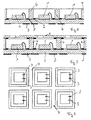
- Fig. 1 shows a sectional side view of devices according to the invention.
- the devices are formed in an array with rows and lines.
- the device comprises a MEMS component 1 mounted on a substrate 2.
- the MEMS component 1 is wire bonded to two contact structures 3 formed as connection pads.
- the wiring bonding is an example, the bonding can be of any other known connection type.
- the MEMS component 1 is surrounded by walls 4.
- the walls 4 and the substrate 2 are made of a ceramic.
- Fig. 1 shows how the devices are manufactured in an array and the walls 4 form a matrix cavity in the shape of a grid having the same spatial dimensions with regard to the surface as the substrate 2.
- the walls 4 are formed from a cavity array.
- the walls 4 are adhesively bonded to substrate 2 using an adhesive 5.
- the devices can be cut into single devices.
- Each of the walls 4 shown in Fig. 1 contributes substantially half of the thickness to one of the devices.
- FIG. 2 A further embodiment is shown in Fig. 2 , where a lid 6 is adhesively bonded to the walls 4.
- the lid 6 is formed of the ceramic used for the walls 4 and the substrate 2.
- the lid 6 has the same dimensions with regard to the area of the surface as the matrix cavity grid of the walls 4 and the substrate 2.
- Fig. 3 shows a top view of the array of Fig. 1 or 2 seen from top.
Landscapes
- Engineering & Computer Science (AREA)
- Microelectronics & Electronic Packaging (AREA)
- Computer Hardware Design (AREA)
- Micromachines (AREA)
Abstract
Description
- The invention relates to a device for supporting a MEMS component, an array of the device, a system comprising the device, a method for manufacturing the device supporting a MEMS component and a use of walls for surrounding a MEMS component.
- It is known to form a so-called MEMS (micro electromechanical system) package (i.e. a packaged electronic module) which comprises a MEMS component which is at least partially surrounded by walls and/or a lid. A device is known which comprises the MEMS component which is supported on a substrate. Most often the substrate is formed of a ceramic or a printed circuit board (PCB). The walls and/or the lid of the known device are formed of plastic, metal or ceramic. However, it has been found that the dimensions, especially the footprint of the device, are difficult to be decreased, especially due to assembly and manufacturing tolerances
- It is an object of the present invention to provide a device for supporting a MEMS component providing the possibility of reducing the footprint of the device. A further object of the present invention is to provide an efficient manufacturable device and a method for manufacturing the same.
- This object is achieved by the subject-matters of the independent patent claims. Further embodiments are shown in the dependent claims as well as the following description.
- The gist of the invention is to use a material for the walls that is similar to the material which is used for the substrate, i.e. a ceramic. The inventors were the first who recognized that when using a ceramic for the substrate, a ceramic cavity array for the walls and/or the lid, thinner walls and/or a thinner lid can be obtained. A ceramic cavity array can be manufactured with high accuracy and addition it can be handled and further processed in a simple manner. When using a ceramic cavity array, the thickness of the walls can be decreased. During manufacturing of the array of the devices a thickness for a wall can be used which is at least two times of the thickness of wall of a single device. When separating the devices each of the walls is used for the two adjacent devices such that the wall thickness is less than the thickness of a wall separating the devices in the array. Further, the walls and/or the lid have a similar coefficient of thermal expansion (CTE) with regard to the substrate.
- According to an embodiment of the invention, a device for supporting a MEMS component is provided. The MEMS component is especially a pressure sensor. The device has a substrate formed of a ceramic, a MEMS component supported on the substrate, and walls forming a cavity for surrounding the MEMS component. The walls are formed of a machined ceramic cavity array. Especially, the walls can be formed of a similar ceramic or the same ceramic as the substrate. The walls could be formed from all kind of ceramic or other rigid material. In a preferred embodiment the two materials have the same or similar coefficient of thermal expansion (CTE) to avoid stress in assembly (preferably less than 10% difference).
- The term "machined" according to the invention encompasses a treatment of at least one wall in which the wall of one of the devices is separated from a wall of a further device. The term "machined" especially encompasses a treatment of cutting, dicing or separating of two of the devices along a wall of one of the devices.
- The walls can be manufactured as a single piece for an array of devices. Thus, four walls surrounding the MEMS component can be unitarily formed, e.g. by laser drilling a ceramic plate-like element in the cavity array. The plate-like element forming the array of cavities can have the same dimension as the substrate forming an array of MEMS components. A simple manufacture process can be obtained.
- The term "supporting" encompasses the formation of a package comprising the MEMS component, wherein the package comprises the substrate, the MEMS component, a contact structure for contacting the MEMS component and a surrounding structure which is mounted on the substrate for at least partially surrounding and/or covering the MEMS component. The walls surrounding the MEMS component can form a cavity for the MEMS component. The walls may have at least one opening so that the at least one opening can lead in or out of the cavity.
- The term "array" according to the invention encompasses a structural element, for example a cavity or a component, which is repeatedly arranged in rows and lines, wherein the number of the structural element in a row and/or a line is at least two.
- The term "similar" according to the invention encompasses the meaning that the materials for the walls and the substrate with regard to the CTE are similar, for example for the CTE to differ by less than 10%. Further, the term "similar" encompasses the meaning that the same material is used for the walls as well as for the substrate.
- The device can further comprise an ASIC (application specific integrated circuit) which can be functionally connected to the MEMS component.
- According to one exemplary embodiment, the walls are connected to the substrate by adhesive bonding. This manner of connection is easy and can be easily implemented in the manufacturing process. The glue can be screen printed on the cavity array, which is then aligned and bonded to the substrate that supports the MEMS components. In a preferred embodiment, epoxy or silicone glue can be used. Preferably, the hole assembly is cured by applying heat in an oven.
- According to one exemplary embodiment, the device has a lid formed from a ceramic for at least partially covering the MEMS component. The lid can comprise openings and/or through-holes which lead in or out of the cavity comprising the MEMS component.
- The device can have a footprint of around 1,5 mm x 1,5 mm, especially preferred around 1,3 mm x 1,4 mm.
- According to one exemplary embodiment, the lid is connected to the walls by adhesive bonding so that the walls as well as the lid can be mounted on the substrate and the walls, respectively, by using a manufacture process which is well known and simply manageable.
- According to one exemplary embodiment, the walls have a thickness of less than 0.2 mm, preferably 0.15 mm. In a preferred exemplary embodiment the walls have a thickness of 0.1 mm.
- According to one aspect of the invention, the invention provides an array of the above-mentioned devices, wherein the device is repeatedly arranged in rows and lines. Such an array can be easily manufactured using processes or process steps which are compatible to those used in microfabrication processes. The cavity array can be laser drilled into a ceramic plate-element.
- In one exemplary embodiment an array of devices is provided, wherein the lid is of substantially the same dimension with regard to the area as the substrate so that the lid does not have to be adapted or matched to one specific device but can be cut into the dimensions for covering the whole array. The term "substantially the same" encompasses according to the invention deviations with regard to tolerance due to the manufacture process, however, a deviation of up to and including +/- 10 % is covered by the term "substantially the same".
- According to a further embodiment of the present invention, a system is provided which comprises the device and a MEMS component, especially a pressure sensor, wherein at least one electrical contact structure is provided to connect the MEMS component. The contact structure can be preferably shaped as a contact pad on the outside of the device, especially the substrate of the device. The contact structure can be connected to the ASIC and/or MEMS component by wire bonding.
- According to a further embodiment of the present invention, a method for manufacturing a device for supporting a MEMS component is provided. The MEMS component can be especially a pressure sensor. The method comprises the step of mounting the MEMS component on a ceramic substrate and the method further comprises the step of providing walls formed of a ceramic surrounding a cavity for the MEMS component, the walls being part of a cavity array.
- According to an exemplary embodiment, the walls are bonded to the substrate by an adhesive.
- According to an exemplary embodiment, the device is cut out of the array.
- According to a further embodiment of the invention, a use of walls for surrounding a MEMS component is provided. The MEMS component can be especially a pressure sensor. The MEMS component is supported on a substrate. The substrate is formed of a ceramic. A ceramic is used for the walls.
- The above description, like the following description of exemplary embodiments is not to be construed as relinquishing specific embodiments of features.
- In the following, the invention will be described in more detail with reference to an embodiment illustrated in the drawings, in which:
- Fig. 1
- is a sectional side view of an array of devices according to the invention;
- Fig. 2
- is a sectional side view of a further embodiment of the array of devices shown in
Fig. 1 ; and - Fig. 3
- is a top view of the array of
Fig. 1 seen from top. -
Fig. 1 shows a sectional side view of devices according to the invention. The devices are formed in an array with rows and lines. The device comprises a MEMS component 1 mounted on asubstrate 2. The MEMS component 1 is wire bonded to twocontact structures 3 formed as connection pads. The wiring bonding is an example, the bonding can be of any other known connection type. The MEMS component 1 is surrounded bywalls 4. Thewalls 4 and thesubstrate 2 are made of a ceramic. -
Fig. 1 shows how the devices are manufactured in an array and thewalls 4 form a matrix cavity in the shape of a grid having the same spatial dimensions with regard to the surface as thesubstrate 2. Thewalls 4 are formed from a cavity array. Thewalls 4 are adhesively bonded tosubstrate 2 using anadhesive 5. - To obtain the single device from the array of devices shown in
Fig. 1 , the devices can be cut into single devices. Each of thewalls 4 shown inFig. 1 contributes substantially half of the thickness to one of the devices. - A further embodiment is shown in
Fig. 2 , where a lid 6 is adhesively bonded to thewalls 4. The lid 6 is formed of the ceramic used for thewalls 4 and thesubstrate 2. The lid 6 has the same dimensions with regard to the area of the surface as the matrix cavity grid of thewalls 4 and thesubstrate 2. -
Fig. 3 shows a top view of the array ofFig. 1 or 2 seen from top.
Claims (13)
- Device for supporting a MEMS component (1), especially a pressure sensor, having
a substrate (2) formed of a ceramic;
a MEMS component (1) on the substrate (2); and
walls (4) forming a cavity for surrounding the MEMS component (1),
characterized in that the walls (4) are formed from a machined ceramic cavity array. - Device of claim 1, characterized in that the walls (4) are connected to the substrate (2) by adhesive bonding.
- Device of claim 1 or 2, characterized in that the device further has a lid (6) formed from a machined stacked ceramic array.
- Device of claim 3, characterized in that the lid (6) is connected to the walls (4) by adhesive bonding.
- Device of anyone of claims 1 to 4, characterized in that the walls (4) have a thickness smaller than 0.2 mm.
- Array of devices according to anyone of claims 1 to 5, characterized in that the device is repeatedly arranged in rows and lines, wherein the number of devices in a row and/or a line is at least 2.
- Array of claim 6, characterized in that the lid (6) is of substantially the same dimension with regard to the area as the substrate (2).
- System comprising the device of anyone of claims 1 to 5, a MEMS component (1), especially a pressure sensor, wherein a contact structure is provided to connect the MEMS component (1) on the outside of the device.
- Method for manufacturing a device for supporting a MEMS component (1), especially a pressure sensor, wherein the method comprises the step of mounting the MEMS component (1) on a ceramic substrate;
the method being characterized by the step of
providing walls (4) formed from a ceramic surrounding a cavity for the MEMS component, the walls being part of a cavity array. - Method according to claim 9, characterized by adhesively bonding the walls (4) to the substrate (2).
- Method according to claim 9 or 10, characterized in that the device is manufactured in rows and lines in the form of an array for the device.
- Method according to claim 11, characterized in that the device is cut out of the array.
- Use of walls (4) for surrounding a MEMS component (1), especially a pressure sensor, the MEMS component (1) on a substrate (2), wherein the substrate (2) is formed from a ceramic, characterized in that a ceramic cavity array is used for the walls (4).
Priority Applications (4)
| Application Number | Priority Date | Filing Date | Title |
|---|---|---|---|
| EP16002203.4A EP3309826B1 (en) | 2016-10-13 | 2016-10-13 | Device for supporting a mems component, array of the device for supporting a system comprising the device, method for manufacturing the device for supporting a mems component and use of walls for surrounding a mems component |
| CN201780062711.3A CN109891574A (en) | 2016-10-13 | 2017-10-12 | It is used to support the device of MEMS component, the array for the device for being used to support the system including the device, for manufacturing the method for supporting the device of MEMS component, and the purposes of the wall around MEMS component |
| US16/341,059 US10988374B2 (en) | 2016-10-13 | 2017-10-12 | Device for supporting a MEMS component |
| PCT/EP2017/076053 WO2018069440A1 (en) | 2016-10-13 | 2017-10-12 | Device for supporting a mems component, array of the device for supporting a system comprising the device, method for manufacturing the device for supporting a mems component and use of walls for surrounding a mems component |
Applications Claiming Priority (1)
| Application Number | Priority Date | Filing Date | Title |
|---|---|---|---|
| EP16002203.4A EP3309826B1 (en) | 2016-10-13 | 2016-10-13 | Device for supporting a mems component, array of the device for supporting a system comprising the device, method for manufacturing the device for supporting a mems component and use of walls for surrounding a mems component |
Publications (2)
| Publication Number | Publication Date |
|---|---|
| EP3309826A1 true EP3309826A1 (en) | 2018-04-18 |
| EP3309826B1 EP3309826B1 (en) | 2025-11-12 |
Family
ID=57178187
Family Applications (1)
| Application Number | Title | Priority Date | Filing Date |
|---|---|---|---|
| EP16002203.4A Active EP3309826B1 (en) | 2016-10-13 | 2016-10-13 | Device for supporting a mems component, array of the device for supporting a system comprising the device, method for manufacturing the device for supporting a mems component and use of walls for surrounding a mems component |
Country Status (4)
| Country | Link |
|---|---|
| US (1) | US10988374B2 (en) |
| EP (1) | EP3309826B1 (en) |
| CN (1) | CN109891574A (en) |
| WO (1) | WO2018069440A1 (en) |
Cited By (1)
| Publication number | Priority date | Publication date | Assignee | Title |
|---|---|---|---|---|
| EP4043391A1 (en) | 2021-02-10 | 2022-08-17 | TE Connectivity Solutions GmbH | Device for supporting mems and/or asic components |
Families Citing this family (2)
| Publication number | Priority date | Publication date | Assignee | Title |
|---|---|---|---|---|
| CN115855236A (en) * | 2022-12-02 | 2023-03-28 | 深海技术科学太湖实验室 | A flexible linear array for testing the pulsating pressure of the turbulent boundary layer in underwater complex interfaces |
| WO2024221210A1 (en) * | 2023-04-25 | 2024-10-31 | 京东方科技集团股份有限公司 | Packaging structure and preparation method therefor, and sensor |
Citations (2)
| Publication number | Priority date | Publication date | Assignee | Title |
|---|---|---|---|---|
| US6384473B1 (en) * | 2000-05-16 | 2002-05-07 | Sandia Corporation | Microelectronic device package with an integral window |
| US20140103518A1 (en) * | 2012-10-15 | 2014-04-17 | Win Semiconductors Corp. | Structure and method for air cavity packaging |
Family Cites Families (6)
| Publication number | Priority date | Publication date | Assignee | Title |
|---|---|---|---|---|
| US5923958A (en) * | 1998-05-28 | 1999-07-13 | Pan Pacific Semiconductor Co., Ltd. | Method for semiconductor chip packaging |
| US6630725B1 (en) * | 2000-10-06 | 2003-10-07 | Motorola, Inc. | Electronic component and method of manufacture |
| US8359927B2 (en) * | 2009-08-12 | 2013-01-29 | Freescale Semiconductor, Inc. | Molded differential PRT pressure sensor |
| US20140374848A1 (en) * | 2013-06-24 | 2014-12-25 | Wen Shi Koh | Semiconductor sensor device with metal lid |
| EP2871152B1 (en) * | 2013-11-06 | 2017-05-24 | Sensirion AG | Sensor device |
| JP6394055B2 (en) * | 2014-05-13 | 2018-09-26 | 日本電気硝子株式会社 | Method for manufacturing ceramic-glass composite package and ceramic-glass composite package |
-
2016
- 2016-10-13 EP EP16002203.4A patent/EP3309826B1/en active Active
-
2017
- 2017-10-12 WO PCT/EP2017/076053 patent/WO2018069440A1/en not_active Ceased
- 2017-10-12 CN CN201780062711.3A patent/CN109891574A/en active Pending
- 2017-10-12 US US16/341,059 patent/US10988374B2/en active Active
Patent Citations (2)
| Publication number | Priority date | Publication date | Assignee | Title |
|---|---|---|---|---|
| US6384473B1 (en) * | 2000-05-16 | 2002-05-07 | Sandia Corporation | Microelectronic device package with an integral window |
| US20140103518A1 (en) * | 2012-10-15 | 2014-04-17 | Win Semiconductors Corp. | Structure and method for air cavity packaging |
Cited By (2)
| Publication number | Priority date | Publication date | Assignee | Title |
|---|---|---|---|---|
| EP4043391A1 (en) | 2021-02-10 | 2022-08-17 | TE Connectivity Solutions GmbH | Device for supporting mems and/or asic components |
| US12116270B2 (en) | 2021-02-10 | 2024-10-15 | Te Connectivity Solutions Gmbh | Device for supporting MEMS and/or ASIC components |
Also Published As
| Publication number | Publication date |
|---|---|
| WO2018069440A1 (en) | 2018-04-19 |
| US10988374B2 (en) | 2021-04-27 |
| EP3309826B1 (en) | 2025-11-12 |
| CN109891574A (en) | 2019-06-14 |
| US20190248648A1 (en) | 2019-08-15 |
Similar Documents
| Publication | Publication Date | Title |
|---|---|---|
| KR100687976B1 (en) | Method for manufacturing an electronic module and an electronic module | |
| US9967972B2 (en) | Circuit board having an asymmetric layer structure | |
| CN102403278B (en) | Connector assembly and manufacture method | |
| US10306750B2 (en) | Circuit board and method for manufacturing a circuit board | |
| EP1898462A2 (en) | Semiconductor apparatus | |
| JP5734434B2 (en) | Wiring board, electronic device and electronic module | |
| DE102005050398A1 (en) | Cavity housing for a mechanically sensitive electronic device and method of manufacture | |
| US10988374B2 (en) | Device for supporting a MEMS component | |
| EP2048109A2 (en) | Electronic device, electronic module, and methods for manufacturing the same | |
| EP2006248B1 (en) | Die mounting stress isolator | |
| JP2007095996A (en) | Semiconductor device | |
| JP5894047B2 (en) | Electronic component storage package | |
| KR101811998B1 (en) | Coupling device, assembly having a coupling device, and method for producing an assembly having a coupling device | |
| JP7455585B2 (en) | How to interconnect sensor units and substrates and carriers | |
| KR101015735B1 (en) | Ceramic laminate module and its manufacturing method | |
| JP2016076669A (en) | Semiconductor element mounting package and method of manufacturing the same, and substrate plate for manufacturing package | |
| JP4613958B2 (en) | Electronic component manufacturing method and electronic component | |
| JP2004128084A (en) | Flake type thermistor and method of manufacturing the same | |
| KR101352603B1 (en) | Mems microphone pcb and method for manufacturing the pcb | |
| JPH1164369A (en) | Semiconductor sensor | |
| KR101015709B1 (en) | Ceramic laminate module and its manufacturing method | |
| JP5376492B2 (en) | Electronic component package and method of manufacturing electronic component package | |
| KR20100104493A (en) | Ltcc package and method of manufacturing the same | |
| JP2006237411A (en) | Semiconductor device and manufacturing method thereof | |
| KR101864577B1 (en) | Sensor module and method for producing a sensor module |
Legal Events
| Date | Code | Title | Description |
|---|---|---|---|
| PUAI | Public reference made under article 153(3) epc to a published international application that has entered the european phase |
Free format text: ORIGINAL CODE: 0009012 |
|
| STAA | Information on the status of an ep patent application or granted ep patent |
Free format text: STATUS: THE APPLICATION HAS BEEN PUBLISHED |
|
| AK | Designated contracting states |
Kind code of ref document: A1 Designated state(s): AL AT BE BG CH CY CZ DE DK EE ES FI FR GB GR HR HU IE IS IT LI LT LU LV MC MK MT NL NO PL PT RO RS SE SI SK SM TR |
|
| AX | Request for extension of the european patent |
Extension state: BA ME |
|
| STAA | Information on the status of an ep patent application or granted ep patent |
Free format text: STATUS: REQUEST FOR EXAMINATION WAS MADE |
|
| 17P | Request for examination filed |
Effective date: 20180924 |
|
| RBV | Designated contracting states (corrected) |
Designated state(s): AL AT BE BG CH CY CZ DE DK EE ES FI FR GB GR HR HU IE IS IT LI LT LU LV MC MK MT NL NO PL PT RO RS SE SI SK SM TR |
|
| STAA | Information on the status of an ep patent application or granted ep patent |
Free format text: STATUS: EXAMINATION IS IN PROGRESS |
|
| 17Q | First examination report despatched |
Effective date: 20190910 |
|
| RAP1 | Party data changed (applicant data changed or rights of an application transferred) |
Owner name: TE CONNECTIVITY SOLUTIONS GMBH |
|
| GRAP | Despatch of communication of intention to grant a patent |
Free format text: ORIGINAL CODE: EPIDOSNIGR1 |
|
| STAA | Information on the status of an ep patent application or granted ep patent |
Free format text: STATUS: GRANT OF PATENT IS INTENDED |
|
| INTG | Intention to grant announced |
Effective date: 20250603 |
|
| GRAS | Grant fee paid |
Free format text: ORIGINAL CODE: EPIDOSNIGR3 |
|
| GRAA | (expected) grant |
Free format text: ORIGINAL CODE: 0009210 |
|
| STAA | Information on the status of an ep patent application or granted ep patent |
Free format text: STATUS: THE PATENT HAS BEEN GRANTED |
|
| AK | Designated contracting states |
Kind code of ref document: B1 Designated state(s): AL AT BE BG CH CY CZ DE DK EE ES FI FR GB GR HR HU IE IS IT LI LT LU LV MC MK MT NL NO PL PT RO RS SE SI SK SM TR |
|
| REG | Reference to a national code |
Ref country code: CH Ref legal event code: F10 Free format text: ST27 STATUS EVENT CODE: U-0-0-F10-F00 (AS PROVIDED BY THE NATIONAL OFFICE) Effective date: 20251112 Ref country code: GB Ref legal event code: FG4D |
|
| REG | Reference to a national code |
Ref country code: DE Ref legal event code: R096 Ref document number: 602016094052 Country of ref document: DE |
|
| REG | Reference to a national code |
Ref country code: DE Ref legal event code: R079 Ref document number: 602016094052 Country of ref document: DE Free format text: PREVIOUS MAIN CLASS: H01L0023000000 Ipc: H10W0099000000 |
|
| REG | Reference to a national code |
Ref country code: IE Ref legal event code: FG4D |
|
| REG | Reference to a national code |
Ref country code: NL Ref legal event code: MP Effective date: 20251112 |
|
| PG25 | Lapsed in a contracting state [announced via postgrant information from national office to epo] |
Ref country code: ES Free format text: LAPSE BECAUSE OF FAILURE TO SUBMIT A TRANSLATION OF THE DESCRIPTION OR TO PAY THE FEE WITHIN THE PRESCRIBED TIME-LIMIT Effective date: 20251112 |
|
| REG | Reference to a national code |
Ref country code: LT Ref legal event code: MG9D |
|
| PG25 | Lapsed in a contracting state [announced via postgrant information from national office to epo] |
Ref country code: NO Free format text: LAPSE BECAUSE OF FAILURE TO SUBMIT A TRANSLATION OF THE DESCRIPTION OR TO PAY THE FEE WITHIN THE PRESCRIBED TIME-LIMIT Effective date: 20260212 |
|
| PG25 | Lapsed in a contracting state [announced via postgrant information from national office to epo] |
Ref country code: HR Free format text: LAPSE BECAUSE OF FAILURE TO SUBMIT A TRANSLATION OF THE DESCRIPTION OR TO PAY THE FEE WITHIN THE PRESCRIBED TIME-LIMIT Effective date: 20251112 Ref country code: AT Free format text: LAPSE BECAUSE OF FAILURE TO SUBMIT A TRANSLATION OF THE DESCRIPTION OR TO PAY THE FEE WITHIN THE PRESCRIBED TIME-LIMIT Effective date: 20251112 Ref country code: FI Free format text: LAPSE BECAUSE OF FAILURE TO SUBMIT A TRANSLATION OF THE DESCRIPTION OR TO PAY THE FEE WITHIN THE PRESCRIBED TIME-LIMIT Effective date: 20251112 |
|
| REG | Reference to a national code |
Ref country code: AT Ref legal event code: MK05 Ref document number: 1857548 Country of ref document: AT Kind code of ref document: T Effective date: 20251112 |
|
| PG25 | Lapsed in a contracting state [announced via postgrant information from national office to epo] |
Ref country code: NL Free format text: LAPSE BECAUSE OF FAILURE TO SUBMIT A TRANSLATION OF THE DESCRIPTION OR TO PAY THE FEE WITHIN THE PRESCRIBED TIME-LIMIT Effective date: 20251112 |
|
| PG25 | Lapsed in a contracting state [announced via postgrant information from national office to epo] |
Ref country code: RS Free format text: LAPSE BECAUSE OF FAILURE TO SUBMIT A TRANSLATION OF THE DESCRIPTION OR TO PAY THE FEE WITHIN THE PRESCRIBED TIME-LIMIT Effective date: 20260212 |
|
| PG25 | Lapsed in a contracting state [announced via postgrant information from national office to epo] |
Ref country code: IS Free format text: LAPSE BECAUSE OF FAILURE TO SUBMIT A TRANSLATION OF THE DESCRIPTION OR TO PAY THE FEE WITHIN THE PRESCRIBED TIME-LIMIT Effective date: 20260312 |
|
| PG25 | Lapsed in a contracting state [announced via postgrant information from national office to epo] |
Ref country code: PT Free format text: LAPSE BECAUSE OF FAILURE TO SUBMIT A TRANSLATION OF THE DESCRIPTION OR TO PAY THE FEE WITHIN THE PRESCRIBED TIME-LIMIT Effective date: 20260312 |
|
| PG25 | Lapsed in a contracting state [announced via postgrant information from national office to epo] |
Ref country code: PL Free format text: LAPSE BECAUSE OF FAILURE TO SUBMIT A TRANSLATION OF THE DESCRIPTION OR TO PAY THE FEE WITHIN THE PRESCRIBED TIME-LIMIT Effective date: 20251112 |
|
| PG25 | Lapsed in a contracting state [announced via postgrant information from national office to epo] |
Ref country code: LV Free format text: LAPSE BECAUSE OF FAILURE TO SUBMIT A TRANSLATION OF THE DESCRIPTION OR TO PAY THE FEE WITHIN THE PRESCRIBED TIME-LIMIT Effective date: 20251112 |
|
| PG25 | Lapsed in a contracting state [announced via postgrant information from national office to epo] |
Ref country code: BG Free format text: LAPSE BECAUSE OF FAILURE TO SUBMIT A TRANSLATION OF THE DESCRIPTION OR TO PAY THE FEE WITHIN THE PRESCRIBED TIME-LIMIT Effective date: 20251112 |
|
| PG25 | Lapsed in a contracting state [announced via postgrant information from national office to epo] |
Ref country code: LT Free format text: LAPSE BECAUSE OF FAILURE TO SUBMIT A TRANSLATION OF THE DESCRIPTION OR TO PAY THE FEE WITHIN THE PRESCRIBED TIME-LIMIT Effective date: 20251112 |
|
| PG25 | Lapsed in a contracting state [announced via postgrant information from national office to epo] |
Ref country code: SM Free format text: LAPSE BECAUSE OF FAILURE TO SUBMIT A TRANSLATION OF THE DESCRIPTION OR TO PAY THE FEE WITHIN THE PRESCRIBED TIME-LIMIT Effective date: 20251112 |
|
| PG25 | Lapsed in a contracting state [announced via postgrant information from national office to epo] |
Ref country code: DK Free format text: LAPSE BECAUSE OF FAILURE TO SUBMIT A TRANSLATION OF THE DESCRIPTION OR TO PAY THE FEE WITHIN THE PRESCRIBED TIME-LIMIT Effective date: 20251112 |
|
| PG25 | Lapsed in a contracting state [announced via postgrant information from national office to epo] |
Ref country code: IT Free format text: LAPSE BECAUSE OF FAILURE TO SUBMIT A TRANSLATION OF THE DESCRIPTION OR TO PAY THE FEE WITHIN THE PRESCRIBED TIME-LIMIT Effective date: 20251112 |
|
| PG25 | Lapsed in a contracting state [announced via postgrant information from national office to epo] |
Ref country code: EE Free format text: LAPSE BECAUSE OF FAILURE TO SUBMIT A TRANSLATION OF THE DESCRIPTION OR TO PAY THE FEE WITHIN THE PRESCRIBED TIME-LIMIT Effective date: 20251112 |
|
| PG25 | Lapsed in a contracting state [announced via postgrant information from national office to epo] |
Ref country code: CZ Free format text: LAPSE BECAUSE OF FAILURE TO SUBMIT A TRANSLATION OF THE DESCRIPTION OR TO PAY THE FEE WITHIN THE PRESCRIBED TIME-LIMIT Effective date: 20251112 |
|
| PG25 | Lapsed in a contracting state [announced via postgrant information from national office to epo] |
Ref country code: SK Free format text: LAPSE BECAUSE OF FAILURE TO SUBMIT A TRANSLATION OF THE DESCRIPTION OR TO PAY THE FEE WITHIN THE PRESCRIBED TIME-LIMIT Effective date: 20251112 |
|
| PG25 | Lapsed in a contracting state [announced via postgrant information from national office to epo] |
Ref country code: SE Free format text: LAPSE BECAUSE OF FAILURE TO SUBMIT A TRANSLATION OF THE DESCRIPTION OR TO PAY THE FEE WITHIN THE PRESCRIBED TIME-LIMIT Effective date: 20251112 |