EP3306670A1 - Semiconductor device structure with non planar slide wall - Google Patents
Semiconductor device structure with non planar slide wall Download PDFInfo
- Publication number
- EP3306670A1 EP3306670A1 EP17181954.3A EP17181954A EP3306670A1 EP 3306670 A1 EP3306670 A1 EP 3306670A1 EP 17181954 A EP17181954 A EP 17181954A EP 3306670 A1 EP3306670 A1 EP 3306670A1
- Authority
- EP
- European Patent Office
- Prior art keywords
- layer
- semiconductor
- dielectric material
- upper portion
- lower portion
- Prior art date
- Legal status (The legal status is an assumption and is not a legal conclusion. Google has not performed a legal analysis and makes no representation as to the accuracy of the status listed.)
- Granted
Links
Images


Classifications
-
- H—ELECTRICITY
- H10—SEMICONDUCTOR DEVICES; ELECTRIC SOLID-STATE DEVICES NOT OTHERWISE PROVIDED FOR
- H10D—INORGANIC ELECTRIC SEMICONDUCTOR DEVICES
- H10D62/00—Semiconductor bodies, or regions thereof, of devices having potential barriers
- H10D62/10—Shapes, relative sizes or dispositions of the regions of the semiconductor bodies; Shapes of the semiconductor bodies
- H10D62/113—Isolations within a component, i.e. internal isolations
- H10D62/115—Dielectric isolations, e.g. air gaps
-
- H—ELECTRICITY
- H10—SEMICONDUCTOR DEVICES; ELECTRIC SOLID-STATE DEVICES NOT OTHERWISE PROVIDED FOR
- H10D—INORGANIC ELECTRIC SEMICONDUCTOR DEVICES
- H10D10/00—Bipolar junction transistors [BJT]
- H10D10/01—Manufacture or treatment
- H10D10/021—Manufacture or treatment of heterojunction BJTs [HBT]
-
- H—ELECTRICITY
- H10—SEMICONDUCTOR DEVICES; ELECTRIC SOLID-STATE DEVICES NOT OTHERWISE PROVIDED FOR
- H10D—INORGANIC ELECTRIC SEMICONDUCTOR DEVICES
- H10D10/00—Bipolar junction transistors [BJT]
- H10D10/01—Manufacture or treatment
- H10D10/051—Manufacture or treatment of vertical BJTs
-
- H—ELECTRICITY
- H10—SEMICONDUCTOR DEVICES; ELECTRIC SOLID-STATE DEVICES NOT OTHERWISE PROVIDED FOR
- H10D—INORGANIC ELECTRIC SEMICONDUCTOR DEVICES
- H10D10/00—Bipolar junction transistors [BJT]
- H10D10/01—Manufacture or treatment
- H10D10/061—Manufacture or treatment of lateral BJTs
-
- H—ELECTRICITY
- H10—SEMICONDUCTOR DEVICES; ELECTRIC SOLID-STATE DEVICES NOT OTHERWISE PROVIDED FOR
- H10D—INORGANIC ELECTRIC SEMICONDUCTOR DEVICES
- H10D10/00—Bipolar junction transistors [BJT]
- H10D10/40—Vertical BJTs
-
- H—ELECTRICITY
- H10—SEMICONDUCTOR DEVICES; ELECTRIC SOLID-STATE DEVICES NOT OTHERWISE PROVIDED FOR
- H10D—INORGANIC ELECTRIC SEMICONDUCTOR DEVICES
- H10D10/00—Bipolar junction transistors [BJT]
- H10D10/60—Lateral BJTs
-
- H—ELECTRICITY
- H10—SEMICONDUCTOR DEVICES; ELECTRIC SOLID-STATE DEVICES NOT OTHERWISE PROVIDED FOR
- H10D—INORGANIC ELECTRIC SEMICONDUCTOR DEVICES
- H10D10/00—Bipolar junction transistors [BJT]
- H10D10/80—Heterojunction BJTs
- H10D10/821—Vertical heterojunction BJTs
-
- H—ELECTRICITY
- H10—SEMICONDUCTOR DEVICES; ELECTRIC SOLID-STATE DEVICES NOT OTHERWISE PROVIDED FOR
- H10D—INORGANIC ELECTRIC SEMICONDUCTOR DEVICES
- H10D62/00—Semiconductor bodies, or regions thereof, of devices having potential barriers
- H10D62/10—Shapes, relative sizes or dispositions of the regions of the semiconductor bodies; Shapes of the semiconductor bodies
- H10D62/13—Semiconductor regions connected to electrodes carrying current to be rectified, amplified or switched, e.g. source or drain regions
- H10D62/137—Collector regions of BJTs
-
- H—ELECTRICITY
- H10—SEMICONDUCTOR DEVICES; ELECTRIC SOLID-STATE DEVICES NOT OTHERWISE PROVIDED FOR
- H10D—INORGANIC ELECTRIC SEMICONDUCTOR DEVICES
- H10D62/00—Semiconductor bodies, or regions thereof, of devices having potential barriers
- H10D62/10—Shapes, relative sizes or dispositions of the regions of the semiconductor bodies; Shapes of the semiconductor bodies
- H10D62/17—Semiconductor regions connected to electrodes not carrying current to be rectified, amplified or switched, e.g. channel regions
- H10D62/177—Base regions of bipolar transistors, e.g. BJTs or IGBTs
-
- H—ELECTRICITY
- H10—SEMICONDUCTOR DEVICES; ELECTRIC SOLID-STATE DEVICES NOT OTHERWISE PROVIDED FOR
- H10D—INORGANIC ELECTRIC SEMICONDUCTOR DEVICES
- H10D62/00—Semiconductor bodies, or regions thereof, of devices having potential barriers
- H10D62/10—Shapes, relative sizes or dispositions of the regions of the semiconductor bodies; Shapes of the semiconductor bodies
- H10D62/17—Semiconductor regions connected to electrodes not carrying current to be rectified, amplified or switched, e.g. channel regions
- H10D62/177—Base regions of bipolar transistors, e.g. BJTs or IGBTs
- H10D62/184—Base regions of bipolar transistors, e.g. BJTs or IGBTs of lateral BJTs
-
- H—ELECTRICITY
- H10—SEMICONDUCTOR DEVICES; ELECTRIC SOLID-STATE DEVICES NOT OTHERWISE PROVIDED FOR
- H10P—GENERIC PROCESSES OR APPARATUS FOR THE MANUFACTURE OR TREATMENT OF DEVICES COVERED BY CLASS H10
- H10P30/00—Ion implantation into wafers, substrates or parts of devices
- H10P30/20—Ion implantation into wafers, substrates or parts of devices into semiconductor materials, e.g. for doping
- H10P30/202—Ion implantation into wafers, substrates or parts of devices into semiconductor materials, e.g. for doping characterised by the semiconductor materials
- H10P30/204—Ion implantation into wafers, substrates or parts of devices into semiconductor materials, e.g. for doping characterised by the semiconductor materials into Group IV semiconductors
-
- H—ELECTRICITY
- H10—SEMICONDUCTOR DEVICES; ELECTRIC SOLID-STATE DEVICES NOT OTHERWISE PROVIDED FOR
- H10P—GENERIC PROCESSES OR APPARATUS FOR THE MANUFACTURE OR TREATMENT OF DEVICES COVERED BY CLASS H10
- H10P30/00—Ion implantation into wafers, substrates or parts of devices
- H10P30/20—Ion implantation into wafers, substrates or parts of devices into semiconductor materials, e.g. for doping
- H10P30/21—Ion implantation into wafers, substrates or parts of devices into semiconductor materials, e.g. for doping of electrically active species
-
- H—ELECTRICITY
- H10—SEMICONDUCTOR DEVICES; ELECTRIC SOLID-STATE DEVICES NOT OTHERWISE PROVIDED FOR
- H10P—GENERIC PROCESSES OR APPARATUS FOR THE MANUFACTURE OR TREATMENT OF DEVICES COVERED BY CLASS H10
- H10P50/00—Etching of wafers, substrates or parts of devices
- H10P50/20—Dry etching; Plasma etching; Reactive-ion etching
- H10P50/28—Dry etching; Plasma etching; Reactive-ion etching of insulating materials
- H10P50/282—Dry etching; Plasma etching; Reactive-ion etching of insulating materials of inorganic materials
- H10P50/283—Dry etching; Plasma etching; Reactive-ion etching of insulating materials of inorganic materials by chemical means
-
- H—ELECTRICITY
- H10—SEMICONDUCTOR DEVICES; ELECTRIC SOLID-STATE DEVICES NOT OTHERWISE PROVIDED FOR
- H10D—INORGANIC ELECTRIC SEMICONDUCTOR DEVICES
- H10D62/00—Semiconductor bodies, or regions thereof, of devices having potential barriers
- H10D62/10—Shapes, relative sizes or dispositions of the regions of the semiconductor bodies; Shapes of the semiconductor bodies
- H10D62/13—Semiconductor regions connected to electrodes carrying current to be rectified, amplified or switched, e.g. source or drain regions
- H10D62/133—Emitter regions of BJTs
- H10D62/136—Emitter regions of BJTs of heterojunction BJTs
-
- H—ELECTRICITY
- H10—SEMICONDUCTOR DEVICES; ELECTRIC SOLID-STATE DEVICES NOT OTHERWISE PROVIDED FOR
- H10P—GENERIC PROCESSES OR APPARATUS FOR THE MANUFACTURE OR TREATMENT OF DEVICES COVERED BY CLASS H10
- H10P30/00—Ion implantation into wafers, substrates or parts of devices
- H10P30/40—Ion implantation into wafers, substrates or parts of devices into insulating materials
Definitions
- This invention relates in general to a semiconductor device and more specifically to a structure of a semiconductor device with a non planar sidewall.
- a semiconductor device such as a transistor utilizes regions of doped semiconductor material to form the structures of the device.
- a bipolar transistor may include an intrinsic base of doped semiconductor material in contact with an intrinsic collector and intrinsic emitter.
- Described herein is a semiconductor structure of a semiconductor device that has a side wall that is non planar and that extends farther outward at an upper portion than at a lower portion of the side wall.
- the semiconductor structure extends underneath a semiconductor layer wherein a top portion of the structure contacts the semiconductor layer.
- the bottom portion of the semiconductor structure contacts an oppositely doped second semiconductor structure below.
- having the upper portion of the semiconductor structure extend out further than the lower portion allows for an increase in the surface area of the semiconductor structure in contact with the semiconductor layer above to reduce the resistance between the two while minimizing the area of the bottom surface of the semiconductor structure to reduce the capacitance with the oppositely doped semiconductor structure below.
- the sidewall is formed by providing an upper portion of a layer of a dielectric material with a faster etch property than a lower portion of the layer.
- the faster etch property is provided by changing the doping profile of the upper portion versus the lower portion (e.g. by ion implantation or by in-situ doping).
- the semiconductor layer is formed over the layer of dielectric material.
- An opening is formed in the layer of semiconductor material wherein the layer of dielectric material is exposed through the opening.
- the layer of dielectric material is isotropically etched through the opening wherein a portion of the layer of dielectric material underneath the layer of semiconductor material is removed.
- the upper portion of the layer of dielectric material is etched at a faster rate due to the dopants such that a side wall of the remaining portion of the layer of dielectric material underneath the layer of semiconductor material has an upper portion that extends laterally farther from the opening than the lower portion of the wall.
- Semiconductor material is formed in a void formed by the etching of the layer of dielectric material such that the newly formed semiconductor material contacts the wall underneath the layer of semiconductor material. Thus, the newly formed semiconductor material extends out farther at an upper portion than at a lower portion underneath the semiconductor layer.
- the newly formed layer of semiconductor material is utilized as an intrinsic base for a bipolar transistor.
- the semiconductor layer is utilized as base electrode structure that couples the intrinsic base to a base contact. Maximizing the upper portion increases the area of contact between the intrinsic base and the base electrode structure to reduce the resistance between the two structures.
- the semiconductor structure below the base is utilized as an intrinsic collector. In some embodiments, reducing the lateral width of the lower portion of the semiconductor structure reduces the capacitance between the intrinsic base and the intrinsic collector below.
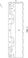
- Figure 1 sets forth a partial cutaway side view of a semiconductor wafer according to one embodiment of the present invention.
- wafer 101 includes a substrate 103 of bulk monocrystalline silicon with regions implanted with dopants and dielectric isolation structures formed therein.
- substrate 103 has a light P type dopant concentration that is formed in-situ with the formation of the substrate or implanted subsequently.
- Region 107 is formed by implanting substrate 103 with N type conductivity dopants (e.g. arsenic, phosphorous).
- N type conductivity dopants e.g. arsenic, phosphorous
- region 107 is implanted with arsenic ion dopants at a dosage of 2.5e 14 /cm 2 and an energy of 450keV, but may be implanted with other dopants, at other dosages, and/or at other energies in other embodiments.
- Region 107 is located over region 105 of substrate 103. At this time, the layers above region 107 (e.g. 135) and region 105 retain the light P dopant profile of substrate 103.
- region 117 is formed by implanting an N type conductivity dopants (e.g. arsenic) into substrate 103.
- the arsenic ion dopants for forming region 117 are implanted at a dosage of 6.2e 15 /cm 2 and an energy of 90keV, but may be implanted with other dopants, at other dosages, and/or at other energies in other embodiments.
- the opening in the mask is used to form a shallow trench isolation structure 109 of a dielectric material (e.g. silicon dioxide).
- the dielectric material may be deposited or thermally grown followed by a planarization of substrate 103.
- the partial cross sectional view of Figure 1 shows four different portions for each of isolation structure 109 and diffusion region 117.
- structure 109 and region 117 would be contiguous across the view of Figure 1 (e.g. at end regions of a transistor).
- the portions of structure 109 and/or the portions of region 117 shown in Figure 1 maybe physically separate from each other.
- collector regions 133, 137, 127, and 131 are formed.
- regions 127 and 131 are selectively implanted (through a patterned mask not shown) with a first N type dopant implant followed by a second N type dopant implant to form regions 133 and 137.
- regions 133 and 137 are formed by implanting arsenic at a dosage of 6.0e 15 /cm 2 and an energy of 20keV, but may be implanted with other dopants, at other dosages, and/or at other energies in other embodiments.
- regions 127 and 131 are formed by implanting phosphorous at a dosage of 1.3e 15 /cm 2 and an energy of 100keV, but may be implanted with other dopants, at other dosages, and/or at other energies in other embodiments.
- regions 133 and 137 are formed separately at a later step.
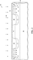
- Figure 2 shows a partial cutaway side view of wafer 101 after oxide layer 201 has been formed on substrate 103 and is implanted with dopants.
- silicon oxide layer 201 is 600 angstroms thick and is deposited by a TEOS process.
- layer 201 may have other thicknesses, be deposited by other processes, and/or be made of other dielectric materials in other embodiments.
- layer 201 may be formed by a thermal oxidation process.
- the implanted dopants 203 are arsenic dopants.
- arsenic dopant ions 203 are implanted into the top third of layer 201 as shown by dashed line 205.
- the arsenic dopant ions may be implanted to other depths in other embodiments.
- the arsenic dopants implanted into the upper portion of layer 201 make the upper portion etch faster than a lower portion of layer 202 during a subsequent selective etching of layer 201. See Figure 5 and its discussion thereof.
- arsenic dopant ions are implanted at a dosage of 5.5e 15 /cm 2 and at an energy of 10keV, but may be implanted at other dosages and/or at other energies in other embodiments.
- the dosage of the dopants may be in the range of 3.0 - 10.0e 15 /cm 2 .
- other types of dopants e.g. phosphorous
- the dopants are introduced in-situ with the formation of layer 201.
- an arsenic precursor is introduced in the deposition chamber during the latter portion of the deposition of layer 201.
- the deposition chamber process conditions during the deposition of layer 201 are modified to increase the etch rate of the upper portion of layer 201 with respect to the lower portion.
- a lower deposition temperature during the deposition of the upper portion of layer 201 results in a less dense oxide with a higher etch in the upper portion of layer 201.
- non-conductivity dopants e.g. xenon, fluorine
- xenon, fluorine may be implanted or introduced into the upper portion of layer 201 to change the etch rate of the upper portion.
- dopants could be implanted or introduced in-situ in the lower portion of layer 201 so that the lower portion of layer 201 etches at a slower rate than the upper portion.
- dopants could be implanted or introduced in-situ in the lower portion of layer 201 so that the lower portion of layer 201 etches at a slower rate than the upper portion.
- boron may be introduced in the lower portion of layer 201 to slow the etch rate relative to the upper portion of layer 201.
- Figure 3 shows a partial cutaway side view of wafer 101 after a layer 301 of polysilicon is formed on layer 201 followed by the deposition of dielectric layers 303, 305, and 307.
- layer 301 is 600 angstroms thick, but may be of other thicknesses in other embodiments.
- Layer 301 is doped with conductivity dopants (e.g. boron) either in-situ or ion implanted (e.g. at a dosage of 1.4e 16 /cm 2 and at an energy of 15 keV).
- conductivity dopants e.g. boron
- layer 303 is an oxide layer (e.g. silicon oxide)
- layer 305 is a nitride layer (e.g. silicon nitride)
- layer 307 is an oxide layer.
- layers 303 and 307 have a thickness of 150 angstroms and layer 305 has a thickness of 500 angstrom, but may have other thicknesses in other embodiments.
- Figure 4 shows a partial cutaway side view of wafer 101 after an opening 401 is formed in layers 305, 303, 301, and 307 and a nitride spacer 403 is formed on the opening side walls.
- the opening is formed by patterning a layer of photo resist or other masking material (not shown) with a corresponding opening and etching layers 301, 303, 305, and 307. Layer 201 is exposed through opening 401.
- opening 401 is formed by etching layers 301, 303, 305, and 307 with the appropriate etchants.
- spacer 403 is made of silicon nitride.
- spacer 403 is formed by forming a layer of silicon nitride (not shown) over wafer 101 and then performing a reactive ion etch to remove the portions of the silicon nitride layer located on the horizontal surfaces of wafer 101. Oxide layer 307 remains on the horizontal surfaces of wafer 101.
- Spacer 403 may be made by other processes and/or other materials in other embodiments.
- Figure 5 shows a partial cutaway side view of wafer 101 after a void 500 is formed in layer 201 and collector region 503 is selectively implanted through opening 401.
- void 500 is formed in layer 201 by performing a wet etch (isotropic) through opening 401 to etch the exposed portions of layer 201.
- this wet etch is performed with hydrofluoric (HF) acid. This wet etch etches out the portion of layer 201 underneath spacer 403 and layer 301 in proximity to opening 401.
- HF hydrofluoric
- the upper portion of layer 201 was implanted with dopants that change the etch rate, the upper portion of layer 201 (that is shown by dashed line 205 etches faster than the lower portion of layer 201 (below line 205).
- layer 201 is silicon oxide
- the upper portion of layer 201 has been implanted with arsenic at a dosage of 5.5e 15 /cm 2 , and where the etchant is HF acid
- the upper portion of layer 201 etches at a rate of 1.7 times faster than the undoped portion of layer 201.
- the upper portion of layer 201 may be etched at a rate that is in the range of 1.3 to 2.5 times faster than the lower portion.
- the etch rates may be different for different layer materials, different etch chemistries, or different dopants in other embodiments.
- layer 307 is also removed.
- the profile of side wall 501 at the upper portion of layer 201 is shown as generally planar along the upper portion above dashed line 205.
- the sidewall of the top surface of the upper portion of layer 201 may not laterally extend as far away from opening 401 as the sidewall at a lower level of the upper portion. Consequently, the widest portion of void 500 may be at a level in the upper portion of layer 201 just below the level of the top surface of layer 201.
- the doping profile in the upper portion of layer 201 is non-uniform, with a higher concentration just below the top surface of layer 201 leading to a higher etch rate and wider void 500 just below the level of the top surface of layer 201.
- lightly doped (or undoped) region 135 is implanted through opening 401 with N type dopant ions (e.g. arsenic, nowadays) to form an intrinsic collector region 503.
- the dopant ions are implanted at an energy of 200keV with a dose of 7.0e 13 /cm 2 such that region 503 extends down to region 107.
- wafer 101 is annealed to activate the dopants of region 503.
- the formation of region 503 occurs after the formation of void 500, but may be performed before the formation of void 500 in other embodiments.
- Figure 6 shows a partial cutaway side view of wafer 101 after a structure 601 of monocrystalline silicon germanium is grown in void 500 including underneath the portions of layer 301.
- structure 601 is formed by an epitaxial growth process where the silicon germanium is grown from the exposed portions of regions 135, 503 and layer 301 by the epitaxial process.
- structure 601 is in-situ doped with a P type dopant (e.g. boron) at a dose of 4.7e 13 /cm 2 .
- structure 601 is also in-situ doped with carbon at a level of 0.04%.
- the germanium content varies from 0% to 30% within structure 601.
- structure 601 may also be formed without carbon or germanium (i.e. only P type silicon). Structure 601 can be formed by other processes and/or be made of other materials (e.g. silicon carbon) in other embodiments.
- wafer 101 Prior to forming structure 601, wafer 101 is subjected to an HF precleaning process.
- Figure 7 shows a partial cutaway side view of wafer 101 after the formation of emitter spacer 701 and polysilicon emitter layer 703.
- spacer 701 is formed on structure 601 next to spacer 403.
- spacer 701 is formed by depositing layers of oxide, nitride, and the oxide (none shown) over wafer 101 and then performing a reactive ion etch to form the spacer.
- the first deposited oxide layer is 150 angstroms
- the nitride layer is 200 angstroms
- the second deposited oxide layer is 500 angstroms, but the layers may be of other thicknesses in other embodiments.
- wafer 101 is subjected to an HF pre-clean that removes from spacer 701, the portion formed from the second deposited oxide layer (not shown) and the remainder of the first deposited oxide layer on structure 601.
- a layer 703 of polysilicon is deposited on wafer 101.
- layer 703 has a thickness of 800 angstroms, but may be of other thicknesses in other embodiments.
- Figure 8 shows a partial cutaway side view of wafer 101 after structures of wafer 101 have been patterned twice.
- the first patterning removes the portions of layers 703, 305 and 303, shown in the view of Figure 8 , outside of area 801. Although not shown in the view of Figure 8 , similar portions of these layers would remain in other areas of wafer 101, e.g. where other semiconductor devices are being formed on wafer 101.
- these layers are patterned by forming a patterned mask (not shown) over wafer 101 with openings outside of area 801. Layers 703, 305, and 303 are then etched (e.g. by a reactive ion etch) through the openings.
- Intrinsic emitter 803 is formed from poly silicon layer 703 as a result of the etching.
- the second patterning of wafer 101 removes the portions of layers 301 and 201 shown in the view of Figure 7 , outside of area 805. Although not shown in the view of Figure 8 , similar portions of these layers would remain in other areas of wafer 101, e.g. where other semiconductor devices are being formed on wafer 101.
- these layers are patterned by forming a patterned mask (not shown) over wafer 101 with openings outside of area 805. Layers 301 and 201 are then etched (e.g. by a reactive ion etch to etch layer 301 followed by an HF wet etch to etch layer 201) through the openings.
- Base electrode structure 807 is formed by the patterning of layer 301. In the cutaway view of Figure 8 , structure 807 includes two portions located on the left and right of spacer 701 where spacer 701 and a portion of emitter 803 are located in an opening of structure 807 such that structure 807 surrounds spacer 701.
- regions 133 and 137 are formed by selectively implanting (through a patterned mask not shown) with an N type dopant implant arsenic at a dosage of 6.0e 15 /cm 2 and an energy of 20keV. Other dopants, at other dosages, and/or at other energies may be implanted in other embodiments.
- wafer 101 is annealed at high temperate to activate and diffuse all the dopants (e.g. of intrinsic base structure 601 and intrinsic emitter 803).
- Figure 9 shows a partial cutaway side view of wafer 101 after silicide structures (901, 902, 903, and 905) are formed on the exposed silicon areas of wafer 101.
- the silicide structures are formed by depositing a layer of metal (e.g. nickel, cobalt) over wafer 101 and heating wafer 101 wherein the metal reacts with the exposed silicon to form the silicide. Afterwards, the unreacted metal is removed.
- metal e.g. nickel, cobalt
- silicide structure 901 is formed on collector contact region 133
- structure 902 is formed on base electrode structure 807
- silicide structure 903 is formed on intrinsic emitter 803
- silicide structure 905 is formed on collector contact region 137.
- Figure 10 shows a partial cutaway side view of wafer 101 after the formation of interconnects to the silicide structures.
- a conformal layer 1002 of dielectric material e.g. nitride
- layer 1002 has a thickness of 500 angstroms, but may be of other thicknesses in other embodiments.
- a relatively thick layer 1003 of oxide e.g. formed by a TEOS process
- planarized e.g. using chemical mechanical polishing. Openings are then formed in layers 1003 and 1002 to expose silicide structures 901, 902, 903, and 905.
- a layer of contact material e.g.
- tungsten, copper is formed over wafer 101 including in the openings and then planarized to form isolated plugs 1005, 1007, 1009, 1011, and 1013.
- the plugs may include barrier metal layers.
- a second dielectric layer 1015 is formed over wafer 101. Openings are formed in layer 1015 to expose conductive plugs 1005, 1007, 1009, 1011, and 1013.
- a layer of interconnect conductive material (e.g. copper) is formed over layer 1015 and subsequently planarized to form interconnect 1017, 1019, 1021, 1023, and 1025.
- the conductive material may include barrier metal layers under the copper.
- Other embodiments may have other conductive structures and/or may be formed in other ways.
- the conductive interconnect structures may electrically couple two or more plugs of plugs 1005, 1007, 1009, 1011, and 1013.
- collector plugs 1005 and 1013 are electrically coupled.
- the transistor formed in water 101 is a bipolar NPN transistor where region 503 is the intrinsic collector and structure 601 is the intrinsic base along with intrinsic emitter 803.
- Intrinsic base structure 601 is electrically accessible from interconnect 1023 via plug 1011, silicide structure 902, and base electrode structure 807 as well as from interconnect 1019 via plug 1007 and silicide structure 902.
- Intrinsic emitter 803 is accessible by interconnect 1021, plug 1009, and silicide structure 903.
- Intrinsic collector region 503 is electrically accessible from interconnect 1025 by plug 1013, silicide structure 905, collector contact region 137, and intermediate collector regions 131, 107, and 117.
- Intrinsic collector region 503 is also electrically accessible from interconnect 1017 by plug 1005, silicide structure 901, collector contact region 133, and intermediate collector regions 127, 107, and 117.
- regions 113 and 137 are physically separated from each other and are implemented in "finger structures" located along isolation structure 109 opposite each side of collector region 503.
- regions 133 and 137 are physically connected at other locations of wafer 101 (e.g. at an end region of the transistor).
- the processes herein may be utilized in forming other types of semiconductor devices such as a PNP bipolar transistor, MOSFET, or diode.
- a PNP bipolar transistor the P type doped regions and the N type doped regions would be switched from the device of Figure 10 .
- interconnect structures may be formed over layer 1015.
- External connectors such as bond pads would be formed on wafer 101.
- wafer 101 is singulated into multiple die with each die including one or more transistors as shown in Figure 10 .
- the die are packaged in semiconductor packages (e.g. leaded, leadless, BGA, QFN, QFP, or wafer level package).
- Figure 11 shows a close up view of the partial cutaway view of Figure 10 .
- Figure 11 shows the distance 1111 that intrinsic base structure 601 extends underneath base electrode structure 807.
- the base resistance between base electrode structure 807 and intrinsic base structure 601 is dependent upon distance 1111, with a greater distance providing for a decrease in resistance.
- the capacitance between the intrinsic base structure 601 and collector region 503 is dependent upon the width 1113 with a smaller width providing for a decrease in capacitance.
- minimizing the width may improve transistor performance in some embodiments by decreasing the base collector capacitance.
- providing a layer of dielectric material with an upper portion and a lower portion having different etch rate properties enables for the formation of an intrinsic base structure with a wider upper portion to decrease the base resistance and a narrower lower portion to decrease the base collector capacitance.
- an intrinsic base region may be formed with a sacrificial dielectric layer having an upper portion and a lower portion that are each etched with the same etchant as opposed to using two layers of different materials. Such methods may reduce the complexity of manufacture of such devices.
- transistors structures described herein can be formed with BICMOS processes, but may be formed by other processes in other embodiments.
- region 503 is underneath structure 601. Although region 503 is at a level of being below the level of layer 201, it is not underneath layer 201.
- intrasic emitter is the structures of a bipolar device that form the PN junctions (the collector/base junction and the base/emitter junction) of the bipolar transistor.
- a method of forming a semiconductor device includes forming a layer of dielectric material. An upper portion of the layer of dielectric material has a first etch rate property with respect to an etchant and a lower portion of the layer of dielectric material has a second etch rate property with respect to the etchant.
- the method includes forming a layer of semiconductor material over the layer of dielectric material and forming an opening in the layer of semiconductor material and exposing the layer of dielectric material through the opening.
- the method includes etching with the etchant, the layer of dielectric material through the opening to remove a portion of the layer of dielectric material underneath the layer of semiconductor material with the etchant.
- the upper portion of the layer of dielectric material is removed by etching with the etchant at a faster rate than the lower portion of the layer of dielectric material is removed by the etching with the etchant such that a remaining side wall of the layer of dielectric material defined by the etching underneath the layer of semiconductor material is non planar with an upper portion of the remaining side wall extending laterally farther from the opening than a lower portion of the remaining side wall extending laterally from the opening.
- the method includes forming a structure of semiconductor material in a location where the layer of dielectric material was removed by the etching.
- the structure extends underneath the layer of semiconductor material to contact a bottom surface of the layer of semiconductor material underneath the layer of semiconductor material.
- the structure has a structure side wall with an upper portion corresponding to the upper portion of the remaining side wall that extends farther underneath the layer of semiconductor material than a lower portion of the structure side wall that corresponds to the lower portion of the remaining side wall.
- the forming a layer of dielectric material includes forming the layer of dielectric material; and implanting dopants into the upper portion of the layer of dielectric material to provide the upper portion of the layer of dielectric material with a higher concentration of the dopants than the lower portion of the layer of dielectric material to provide the upper portion with the first etch rate property with respect to the second etch rate property.
- the forming the layer of dielectric material includes in-situ doping the upper portion with dopants to provide the upper portion of the layer of dielectric material with a higher concentration of the dopants than the lower portion of the layer of dielectric material to provide the upper portion with the first etch rate property with respect to the second etch rate property.
- the semiconductor device includes a second structure of semiconductor material underneath and in contact with the structure of semiconductor material, wherein the structure of semiconductor material has a first conductivity doping profile that is opposite a conductivity doping profile of the second structure of semiconductor material.
- the structure of semiconductor material is characterized as an intrinsic base of the semiconductor device and the second structure of semiconductor material is characterized as an intrinsic collector of the semiconductor device.
- the second structure of semiconductor material includes conductivity dopants implanted into a layer of semiconductor material through the opening.
- the structure of semiconductor material is characterized as an intrinsic base of the semiconductor device wherein a portion of the layer of semiconductor material in which the structure of semiconductor material is located underneath is characterized as a base electrode of the semiconductor device.
- the dielectric material is characterized as an oxide.
- the etchant includes hydrofluoric (HF) acid.
- the etching includes etching the upper portion of the layer of dielectric material with the etchant at a first rate and etching the lower portion of the dielectric material by with the etchant at a second rate, wherein the first rate is in a range 1.3 to 2.5 times faster than the second rate.
- the upper portion of the layer of dielectric material has a higher concentration of dopants than the lower portion of the layer of dielectric material to provide the upper portion with the first etch rate property with respect to the second etch rate property.
- the dopants include arsenic at a concentration in the upper portion in the range of 1.0e20 to 1.0e22 /cm 3 .
- the lower portion of the layer of dielectric material has a higher concentration of dopants than the upper portion of the layer of dielectric material to provide the lower portion with the second etch rate property with respect to the first etch rate property.
- forming a further structure of semiconductor material over and in contact with the structure, wherein at least a portion of the further structure is located in the opening wherein the structure of semiconductor material is characterized as an intrinsic base of the semiconductor device and the further structure is characterized as an intrinsic emitter of the semiconductor device.
- a semiconductor device in another embodiment, includes a first semiconductor structure and a second semiconductor structure having a first side wall. A portion of the first semiconductor structure extends underneath the second semiconductor structure from the first side wall and has a top surface in contact with a bottom surface of the second semiconductor structure underneath the second semiconductor structure.
- the semiconductor device includes a layer of dielectric material underneath the second semiconductor structure. The layer of dielectric material has a second side wall laterally in contact with the portion of the first semiconductor structure.
- the first semiconductor structure has an upper portion and a lower portion, wherein the upper portion is wider than the lower portion and wherein the upper portion of the first semiconductor structure contacts an upper portion of the layer of dielectric material at the second side wall and the lower portion of the first semiconductor structure contacts a lower portion of the layer of dielectric material at the second side wall.
- the upper portion of the layer of dielectric material has a first etch rate property that etches at a first rate with an etchant and the lower portion of the layer of dielectric material has a second etch rate property that etches at a second rate with the etchant.
- the first rate is faster than the second rate.
- the dielectric material is characterized as an oxide.
- the etchant includes hydrofluoric (HF) acid.
- the upper portion of the layer of dielectric material has a higher concentration of dopants than the lower portion of the layer of dielectric material to provide the upper portion with the first etch rate property with respect to the second etch rate property.
- the dopants include arsenic.
- the first semiconductor structure is characterized as an intrinsic base of a bipolar transistor and the second semiconductor structure is characterized as a base electrode of the semiconductor device, wherein the semiconductor device includes an intrinsic collector located underneath the intrinsic base.
Landscapes
- Electrodes Of Semiconductors (AREA)
- Bipolar Transistors (AREA)
- Chemical & Material Sciences (AREA)
- Chemical Kinetics & Catalysis (AREA)
- General Chemical & Material Sciences (AREA)
- Internal Circuitry In Semiconductor Integrated Circuit Devices (AREA)
- Non-Volatile Memory (AREA)
Abstract
Description
- This invention relates in general to a semiconductor device and more specifically to a structure of a semiconductor device with a non planar sidewall.
- A semiconductor device such as a transistor utilizes regions of doped semiconductor material to form the structures of the device. For example, a bipolar transistor may include an intrinsic base of doped semiconductor material in contact with an intrinsic collector and intrinsic emitter.
- The present invention may be better understood, and its numerous objects, features, and advantages made apparent to those skilled in the art by referencing the accompanying drawings.
-
Figures 1-10 show partial cutaway side views at various stages in the manufacture of a semiconductor device according to one embodiment of the present invention. -
Figure 11 is a partial cut away side view of a semiconductor device according to one embodiment of the present invention. - The use of the same reference symbols in different drawings indicates identical items unless otherwise noted. The Figures are not necessarily drawn to scale.
- The following sets forth a detailed description of a mode for carrying out the invention. The description is intended to be illustrative of the invention and should not be taken to be limiting.
- Described herein is a semiconductor structure of a semiconductor device that has a side wall that is non planar and that extends farther outward at an upper portion than at a lower portion of the side wall. The semiconductor structure extends underneath a semiconductor layer wherein a top portion of the structure contacts the semiconductor layer. The bottom portion of the semiconductor structure contacts an oppositely doped second semiconductor structure below. In one embodiment, having the upper portion of the semiconductor structure extend out further than the lower portion allows for an increase in the surface area of the semiconductor structure in contact with the semiconductor layer above to reduce the resistance between the two while minimizing the area of the bottom surface of the semiconductor structure to reduce the capacitance with the oppositely doped semiconductor structure below.
- In one example, the sidewall is formed by providing an upper portion of a layer of a dielectric material with a faster etch property than a lower portion of the layer. In one embodiment, the faster etch property is provided by changing the doping profile of the upper portion versus the lower portion (e.g. by ion implantation or by in-situ doping). The semiconductor layer is formed over the layer of dielectric material. An opening is formed in the layer of semiconductor material wherein the layer of dielectric material is exposed through the opening. The layer of dielectric material is isotropically etched through the opening wherein a portion of the layer of dielectric material underneath the layer of semiconductor material is removed. In one embodiment, the upper portion of the layer of dielectric material is etched at a faster rate due to the dopants such that a side wall of the remaining portion of the layer of dielectric material underneath the layer of semiconductor material has an upper portion that extends laterally farther from the opening than the lower portion of the wall. Semiconductor material is formed in a void formed by the etching of the layer of dielectric material such that the newly formed semiconductor material contacts the wall underneath the layer of semiconductor material. Thus, the newly formed semiconductor material extends out farther at an upper portion than at a lower portion underneath the semiconductor layer.
- In one embodiment, the newly formed layer of semiconductor material is utilized as an intrinsic base for a bipolar transistor. The semiconductor layer is utilized as base electrode structure that couples the intrinsic base to a base contact. Maximizing the upper portion increases the area of contact between the intrinsic base and the base electrode structure to reduce the resistance between the two structures. In some embodiments, the semiconductor structure below the base is utilized as an intrinsic collector. In some embodiments, reducing the lateral width of the lower portion of the semiconductor structure reduces the capacitance between the intrinsic base and the intrinsic collector below.
-
Figure 1 sets forth a partial cutaway side view of a semiconductor wafer according to one embodiment of the present invention. In one embodiment,wafer 101 includes asubstrate 103 of bulk monocrystalline silicon with regions implanted with dopants and dielectric isolation structures formed therein. In one embodiment,substrate 103 has a light P type dopant concentration that is formed in-situ with the formation of the substrate or implanted subsequently.Region 107 is formed by implantingsubstrate 103 with N type conductivity dopants (e.g. arsenic, phosphorous). In oneembodiment region 107 is implanted with arsenic ion dopants at a dosage of 2.5e14 /cm2 and an energy of 450keV, but may be implanted with other dopants, at other dosages, and/or at other energies in other embodiments.Region 107 is located overregion 105 ofsubstrate 103. At this time, the layers above region 107 (e.g. 135) andregion 105 retain the light P dopant profile ofsubstrate 103. - Next, a mask (not shown) is formed over
wafer 101 with an opening for implantingcollector diffusion region 117. In one embodiment,region 117 is formed by implanting an N type conductivity dopants (e.g. arsenic) intosubstrate 103. In one embodiment, the arsenic ion dopants for formingregion 117 are implanted at a dosage of 6.2e15 /cm2 and an energy of 90keV, but may be implanted with other dopants, at other dosages, and/or at other energies in other embodiments. Afterwards, the opening in the mask is used to form a shallowtrench isolation structure 109 of a dielectric material (e.g. silicon dioxide). In one embodiment, the dielectric material may be deposited or thermally grown followed by a planarization ofsubstrate 103. The partial cross sectional view ofFigure 1 shows four different portions for each ofisolation structure 109 anddiffusion region 117. However, at other cross sections ofwafer 101, (located into or out of the page from the view ofFigure 1 ),structure 109 andregion 117 would be contiguous across the view ofFigure 1 (e.g. at end regions of a transistor). However, in other embodiments, the portions ofstructure 109 and/or the portions ofregion 117 shown inFigure 1 maybe physically separate from each other. - After the formation of
isolation structure 109,collector regions regions regions regions regions regions -
Figure 2 shows a partial cutaway side view ofwafer 101 afteroxide layer 201 has been formed onsubstrate 103 and is implanted with dopants. In one embodiment,silicon oxide layer 201 is 600 angstroms thick and is deposited by a TEOS process. However,layer 201 may have other thicknesses, be deposited by other processes, and/or be made of other dielectric materials in other embodiments. For example,layer 201 may be formed by a thermal oxidation process. - In one embodiment, the implanted
dopants 203 are arsenic dopants. In one embodiment,arsenic dopant ions 203 are implanted into the top third oflayer 201 as shown by dashedline 205. However, the arsenic dopant ions may be implanted to other depths in other embodiments. The arsenic dopants implanted into the upper portion oflayer 201 make the upper portion etch faster than a lower portion of layer 202 during a subsequent selective etching oflayer 201. SeeFigure 5 and its discussion thereof. In one embodiment, arsenic dopant ions are implanted at a dosage of 5.5e15 /cm2 and at an energy of 10keV, but may be implanted at other dosages and/or at other energies in other embodiments. For example, the dosage of the dopants may be in the range of 3.0 - 10.0e15/cm2. Also in other embodiments, other types of dopants (e.g. phosphorous) may be implanted intolayer 201 to increase the etching rate. - In another embodiment, the dopants (e.g. arsenic) are introduced in-situ with the formation of
layer 201. In one embodiment, an arsenic precursor is introduced in the deposition chamber during the latter portion of the deposition oflayer 201. In other embodiments, the deposition chamber process conditions during the deposition oflayer 201 are modified to increase the etch rate of the upper portion oflayer 201 with respect to the lower portion. In one embodiment, a lower deposition temperature during the deposition of the upper portion oflayer 201 results in a less dense oxide with a higher etch in the upper portion oflayer 201. - In other embodiments, non-conductivity dopants (e.g. xenon, fluorine) may be implanted or introduced into the upper portion of
layer 201 to change the etch rate of the upper portion. - Still in other embodiments, dopants could be implanted or introduced in-situ in the lower portion of
layer 201 so that the lower portion oflayer 201 etches at a slower rate than the upper portion. For example, boron may be introduced in the lower portion oflayer 201 to slow the etch rate relative to the upper portion oflayer 201. -
Figure 3 shows a partial cutaway side view ofwafer 101 after alayer 301 of polysilicon is formed onlayer 201 followed by the deposition ofdielectric layers layer 301 is 600 angstroms thick, but may be of other thicknesses in other embodiments.Layer 301 is doped with conductivity dopants (e.g. boron) either in-situ or ion implanted (e.g. at a dosage of 1.4e16/cm2 and at an energy of 15 keV). - In one embodiment,
layer 303 is an oxide layer (e.g. silicon oxide),layer 305 is a nitride layer (e.g. silicon nitride), andlayer 307 is an oxide layer. In one embodiment, layers 303 and 307 have a thickness of 150 angstroms andlayer 305 has a thickness of 500 angstrom, but may have other thicknesses in other embodiments. -
Figure 4 shows a partial cutaway side view ofwafer 101 after anopening 401 is formed inlayers nitride spacer 403 is formed on the opening side walls. In one embodiment, the opening is formed by patterning a layer of photo resist or other masking material (not shown) with a corresponding opening andetching layers Layer 201 is exposed throughopening 401. In one embodiment, opening 401 is formed by etchinglayers - In the embodiment shown,
spacer 403 is made of silicon nitride. In one embodiment,spacer 403 is formed by forming a layer of silicon nitride (not shown) overwafer 101 and then performing a reactive ion etch to remove the portions of the silicon nitride layer located on the horizontal surfaces ofwafer 101.Oxide layer 307 remains on the horizontal surfaces ofwafer 101.Spacer 403 may be made by other processes and/or other materials in other embodiments. -
Figure 5 shows a partial cutaway side view ofwafer 101 after avoid 500 is formed inlayer 201 andcollector region 503 is selectively implanted throughopening 401. In one embodiment, void 500 is formed inlayer 201 by performing a wet etch (isotropic) throughopening 401 to etch the exposed portions oflayer 201. In one embodiment, this wet etch is performed with hydrofluoric (HF) acid. This wet etch etches out the portion oflayer 201 underneathspacer 403 andlayer 301 in proximity toopening 401. Because the upper portion oflayer 201 was implanted with dopants that change the etch rate, the upper portion of layer 201 (that is shown by dashedline 205 etches faster than the lower portion of layer 201 (below line 205). In one embodiment wherelayer 201 is silicon oxide, where the upper portion oflayer 201 has been implanted with arsenic at a dosage of 5.5e15/cm2, and where the etchant is HF acid, the upper portion oflayer 201 etches at a rate of 1.7 times faster than the undoped portion oflayer 201. In other embodiments, the upper portion oflayer 201 may be etched at a rate that is in the range of 1.3 to 2.5 times faster than the lower portion. However, the etch rates may be different for different layer materials, different etch chemistries, or different dopants in other embodiments. During the etching oflayer 201,layer 307 is also removed. - In the embodiment shown, the profile of
side wall 501 at the upper portion oflayer 201 is shown as generally planar along the upper portion above dashedline 205. However, with some embodiments, the sidewall of the top surface of the upper portion oflayer 201 may not laterally extend as far away from opening 401 as the sidewall at a lower level of the upper portion. Consequently, the widest portion ofvoid 500 may be at a level in the upper portion oflayer 201 just below the level of the top surface oflayer 201. In one embodiment, the doping profile in the upper portion oflayer 201 is non-uniform, with a higher concentration just below the top surface oflayer 201 leading to a higher etch rate andwider void 500 just below the level of the top surface oflayer 201. - In one embodiment, lightly doped (or undoped)
region 135 is implanted throughopening 401 with N type dopant ions (e.g. arsenic, prosperous) to form anintrinsic collector region 503. In one embodiment, the dopant ions are implanted at an energy of 200keV with a dose of 7.0e13 /cm2 such thatregion 503 extends down toregion 107. Afterwards,wafer 101 is annealed to activate the dopants ofregion 503. In one embodiment, the formation ofregion 503 occurs after the formation ofvoid 500, but may be performed before the formation ofvoid 500 in other embodiments. -
Figure 6 shows a partial cutaway side view ofwafer 101 after astructure 601 of monocrystalline silicon germanium is grown invoid 500 including underneath the portions oflayer 301. In one embodiment,structure 601 is formed by an epitaxial growth process where the silicon germanium is grown from the exposed portions ofregions layer 301 by the epitaxial process. In one embodiment,structure 601 is in-situ doped with a P type dopant (e.g. boron) at a dose of 4.7e13 /cm2. In one embodiment,structure 601 is also in-situ doped with carbon at a level of 0.04%. In one embodiment, the germanium content varies from 0% to 30% withinstructure 601. However,structure 601 may also be formed without carbon or germanium (i.e. only P type silicon).Structure 601 can be formed by other processes and/or be made of other materials (e.g. silicon carbon) in other embodiments. Prior to formingstructure 601,wafer 101 is subjected to an HF precleaning process. -
Figure 7 shows a partial cutaway side view ofwafer 101 after the formation ofemitter spacer 701 andpolysilicon emitter layer 703. In the embodiment shown,spacer 701 is formed onstructure 601 next tospacer 403. In one embodiment,spacer 701 is formed by depositing layers of oxide, nitride, and the oxide (none shown) overwafer 101 and then performing a reactive ion etch to form the spacer. In one embodiment, the first deposited oxide layer is 150 angstroms, the nitride layer is 200 angstroms, and the second deposited oxide layer is 500 angstroms, but the layers may be of other thicknesses in other embodiments. After the reactive ion etching,wafer 101 is subjected to an HF pre-clean that removes fromspacer 701, the portion formed from the second deposited oxide layer (not shown) and the remainder of the first deposited oxide layer onstructure 601. - After the formation of
spacer 701, alayer 703 of polysilicon is deposited onwafer 101. In one embodiment,layer 703 has a thickness of 800 angstroms, but may be of other thicknesses in other embodiments. -
Figure 8 shows a partial cutaway side view ofwafer 101 after structures ofwafer 101 have been patterned twice. The first patterning removes the portions oflayers Figure 8 , outside ofarea 801. Although not shown in the view ofFigure 8 , similar portions of these layers would remain in other areas ofwafer 101, e.g. where other semiconductor devices are being formed onwafer 101. In one embodiment, these layers are patterned by forming a patterned mask (not shown) overwafer 101 with openings outside ofarea 801.Layers Intrinsic emitter 803 is formed frompoly silicon layer 703 as a result of the etching. - The second patterning of
wafer 101 removes the portions oflayers Figure 7 , outside ofarea 805. Although not shown in the view ofFigure 8 , similar portions of these layers would remain in other areas ofwafer 101, e.g. where other semiconductor devices are being formed onwafer 101. In one embodiment, these layers are patterned by forming a patterned mask (not shown) overwafer 101 with openings outside ofarea 805.Layers layer 301 followed by an HF wet etch to etch layer 201) through the openings.Base electrode structure 807 is formed by the patterning oflayer 301. In the cutaway view ofFigure 8 ,structure 807 includes two portions located on the left and right ofspacer 701 wherespacer 701 and a portion ofemitter 803 are located in an opening ofstructure 807 such thatstructure 807 surroundsspacer 701. - At this point, in one embodiment,
regions wafer 101 is annealed at high temperate to activate and diffuse all the dopants (e.g. ofintrinsic base structure 601 and intrinsic emitter 803). -
Figure 9 shows a partial cutaway side view ofwafer 101 after silicide structures (901, 902, 903, and 905) are formed on the exposed silicon areas ofwafer 101. In one embodiment, the silicide structures are formed by depositing a layer of metal (e.g. nickel, cobalt) overwafer 101 andheating wafer 101 wherein the metal reacts with the exposed silicon to form the silicide. Afterwards, the unreacted metal is removed. InFigure 9 ,silicide structure 901 is formed oncollector contact region 133,structure 902 is formed onbase electrode structure 807,silicide structure 903 is formed onintrinsic emitter 803, andsilicide structure 905 is formed oncollector contact region 137. -
Figure 10 shows a partial cutaway side view ofwafer 101 after the formation of interconnects to the silicide structures. After the formation ofsilicide structures conformal layer 1002 of dielectric material (e.g. nitride) is formed overwafer 101. In one embodiment,layer 1002 has a thickness of 500 angstroms, but may be of other thicknesses in other embodiments. Afterwards a relativelythick layer 1003 of oxide (e.g. formed by a TEOS process) is formed overlayer 1002 and planarized (e.g. using chemical mechanical polishing). Openings are then formed inlayers silicide structures wafer 101 including in the openings and then planarized to formisolated plugs second dielectric layer 1015 is formed overwafer 101. Openings are formed inlayer 1015 to exposeconductive plugs layer 1015 and subsequently planarized to forminterconnect plugs - In the embodiment shown, the transistor formed in
water 101 is a bipolar NPN transistor whereregion 503 is the intrinsic collector andstructure 601 is the intrinsic base along withintrinsic emitter 803.Intrinsic base structure 601 is electrically accessible frominterconnect 1023 viaplug 1011,silicide structure 902, andbase electrode structure 807 as well as frominterconnect 1019 viaplug 1007 andsilicide structure 902.Intrinsic emitter 803 is accessible byinterconnect 1021,plug 1009, andsilicide structure 903.Intrinsic collector region 503 is electrically accessible frominterconnect 1025 byplug 1013,silicide structure 905,collector contact region 137, andintermediate collector regions Intrinsic collector region 503 is also electrically accessible frominterconnect 1017 byplug 1005,silicide structure 901,collector contact region 133, andintermediate collector regions regions silicide structures 901 and 905) are physically separated from each other and are implemented in "finger structures" located alongisolation structure 109 opposite each side ofcollector region 503. However in other embodiments,regions 133 and 137 (as well asregions silicide structures 901 and 905) are physically connected at other locations of wafer 101 (e.g. at an end region of the transistor). - The processes herein may be utilized in forming other types of semiconductor devices such as a PNP bipolar transistor, MOSFET, or diode. In one embodiment of forming a PNP bipolar transistor, the P type doped regions and the N type doped regions would be switched from the device of
Figure 10 . - After the stage of
Figure 10 , further interconnect structures may be formed overlayer 1015. External connectors such as bond pads would be formed onwafer 101. Afterwards,wafer 101 is singulated into multiple die with each die including one or more transistors as shown inFigure 10 . Afterwards, the die are packaged in semiconductor packages (e.g. leaded, leadless, BGA, QFN, QFP, or wafer level package). -
Figure 11 shows a close up view of the partial cutaway view ofFigure 10 .Figure 11 shows thedistance 1111 thatintrinsic base structure 601 extends underneathbase electrode structure 807. The base resistance betweenbase electrode structure 807 andintrinsic base structure 601 is dependent upondistance 1111, with a greater distance providing for a decrease in resistance. The capacitance between theintrinsic base structure 601 andcollector region 503 is dependent upon thewidth 1113 with a smaller width providing for a decrease in capacitance. Thus, minimizing the width may improve transistor performance in some embodiments by decreasing the base collector capacitance. - In some embodiments, providing a layer of dielectric material with an upper portion and a lower portion having different etch rate properties enables for the formation of an intrinsic base structure with a wider upper portion to decrease the base resistance and a narrower lower portion to decrease the base collector capacitance. With some embodiments of the methods described herein, such an intrinsic base region may be formed with a sacrificial dielectric layer having an upper portion and a lower portion that are each etched with the same etchant as opposed to using two layers of different materials. Such methods may reduce the complexity of manufacture of such devices.
- The transistors structures described herein can be formed with BICMOS processes, but may be formed by other processes in other embodiments.
- As used herein, the term "underneath" means directly below. For example, in the view of
Figure 11 ,region 503 is underneathstructure 601. Althoughregion 503 is at a level of being below the level oflayer 201, it is not underneathlayer 201. - The terms "intrinsic emitter," "intrinsic base," and "intrinsic collector" are the structures of a bipolar device that form the PN junctions (the collector/base junction and the base/emitter junction) of the bipolar transistor.
- In one embodiment, a method of forming a semiconductor device includes forming a layer of dielectric material. An upper portion of the layer of dielectric material has a first etch rate property with respect to an etchant and a lower portion of the layer of dielectric material has a second etch rate property with respect to the etchant. The method includes forming a layer of semiconductor material over the layer of dielectric material and forming an opening in the layer of semiconductor material and exposing the layer of dielectric material through the opening. The method includes etching with the etchant, the layer of dielectric material through the opening to remove a portion of the layer of dielectric material underneath the layer of semiconductor material with the etchant. The upper portion of the layer of dielectric material is removed by etching with the etchant at a faster rate than the lower portion of the layer of dielectric material is removed by the etching with the etchant such that a remaining side wall of the layer of dielectric material defined by the etching underneath the layer of semiconductor material is non planar with an upper portion of the remaining side wall extending laterally farther from the opening than a lower portion of the remaining side wall extending laterally from the opening. The method includes forming a structure of semiconductor material in a location where the layer of dielectric material was removed by the etching. The structure extends underneath the layer of semiconductor material to contact a bottom surface of the layer of semiconductor material underneath the layer of semiconductor material. The structure has a structure side wall with an upper portion corresponding to the upper portion of the remaining side wall that extends farther underneath the layer of semiconductor material than a lower portion of the structure side wall that corresponds to the lower portion of the remaining side wall.
- In an example, the forming a layer of dielectric material includes forming the layer of dielectric material; and implanting dopants into the upper portion of the layer of dielectric material to provide the upper portion of the layer of dielectric material with a higher concentration of the dopants than the lower portion of the layer of dielectric material to provide the upper portion with the first etch rate property with respect to the second etch rate property. In an example, the forming the layer of dielectric material includes in-situ doping the upper portion with dopants to provide the upper portion of the layer of dielectric material with a higher concentration of the dopants than the lower portion of the layer of dielectric material to provide the upper portion with the first etch rate property with respect to the second etch rate property. In an example, the semiconductor device includes a second structure of semiconductor material underneath and in contact with the structure of semiconductor material, wherein the structure of semiconductor material has a first conductivity doping profile that is opposite a conductivity doping profile of the second structure of semiconductor material. In an example, the structure of semiconductor material is characterized as an intrinsic base of the semiconductor device and the second structure of semiconductor material is characterized as an intrinsic collector of the semiconductor device. In an example, the second structure of semiconductor material includes conductivity dopants implanted into a layer of semiconductor material through the opening. In an example, the structure of semiconductor material is characterized as an intrinsic base of the semiconductor device wherein a portion of the layer of semiconductor material in which the structure of semiconductor material is located underneath is characterized as a base electrode of the semiconductor device. In an example, the dielectric material is characterized as an oxide. In an example, the etchant includes hydrofluoric (HF) acid. In an example, the etching includes etching the upper portion of the layer of dielectric material with the etchant at a first rate and etching the lower portion of the dielectric material by with the etchant at a second rate, wherein the first rate is in a range 1.3 to 2.5 times faster than the second rate. In an example, the upper portion of the layer of dielectric material has a higher concentration of dopants than the lower portion of the layer of dielectric material to provide the upper portion with the first etch rate property with respect to the second etch rate property. In an example, the dopants include arsenic at a concentration in the upper portion in the range of 1.0e20 to 1.0e22 /cm3. In an example, the lower portion of the layer of dielectric material has a higher concentration of dopants than the upper portion of the layer of dielectric material to provide the lower portion with the second etch rate property with respect to the first etch rate property. In an example, after forming the structure of semiconductor material, forming a further structure of semiconductor material over and in contact with the structure, wherein at least a portion of the further structure is located in the opening, wherein the structure of semiconductor material is characterized as an intrinsic base of the semiconductor device and the further structure is characterized as an intrinsic emitter of the semiconductor device.
- In another embodiment, a semiconductor device includes a first semiconductor structure and a second semiconductor structure having a first side wall. A portion of the first semiconductor structure extends underneath the second semiconductor structure from the first side wall and has a top surface in contact with a bottom surface of the second semiconductor structure underneath the second semiconductor structure. The semiconductor device includes a layer of dielectric material underneath the second semiconductor structure. The layer of dielectric material has a second side wall laterally in contact with the portion of the first semiconductor structure. The first semiconductor structure has an upper portion and a lower portion, wherein the upper portion is wider than the lower portion and wherein the upper portion of the first semiconductor structure contacts an upper portion of the layer of dielectric material at the second side wall and the lower portion of the first semiconductor structure contacts a lower portion of the layer of dielectric material at the second side wall. The upper portion of the layer of dielectric material has a first etch rate property that etches at a first rate with an etchant and the lower portion of the layer of dielectric material has a second etch rate property that etches at a second rate with the etchant. The first rate is faster than the second rate.
- In an example, the dielectric material is characterized as an oxide. In an example, the etchant includes hydrofluoric (HF) acid. In an example, the upper portion of the layer of dielectric material has a higher concentration of dopants than the lower portion of the layer of dielectric material to provide the upper portion with the first etch rate property with respect to the second etch rate property. In an example, the dopants include arsenic. In an example, the first semiconductor structure is characterized as an intrinsic base of a bipolar transistor and the second semiconductor structure is characterized as a base electrode of the semiconductor device, wherein the semiconductor device includes an intrinsic collector located underneath the intrinsic base.
- While particular embodiments of the present invention have been shown and described, it will be recognized to those skilled in the art that, based upon the teachings herein, further changes and modifications may be made without departing from this invention and its broader aspects, and thus, the appended claims are to encompass within their scope all such changes and modifications as are within the true spirit and scope of this invention.
Claims (15)
- A method of forming a semiconductor device comprising:forming a layer (201) of dielectric material, wherein an upper portion of the layer (201) of dielectric material has a first etch rate property with respect to an etchant and a lower portion of the layer (201) of dielectric material has a second etch rate property with respect to the etchant;forming a layer (301) of semiconductor material over the layer (201) of dielectric material;forming an opening (401) in the layer (301) of semiconductor material and exposing the layer (201) of dielectric material through the opening;etching with the etchant, the layer (201) of dielectric material through the opening to remove a portion of the layer (201) of dielectric material underneath the layer (301) of semiconductor material with the etchant, wherein the upper portion of the layer (201) of dielectric material is removed by etching with the etchant at a faster rate than the lower portion of the layer (201) of dielectric material is removed by the etching with the etchant such that a remaining side wall (501) of the layer (201) of dielectric material defined by the etching underneath the layer (301) of semiconductor material is non planar with an upper portion of the remaining side wall (501) extending laterally farther from the opening than a lower portion of the remaining side wall (501) extending laterally from the opening;forming a structure (601) of semiconductor material in a location where the layer (201) of dielectric material was removed by the etching, wherein the structure extends underneath the layer (301) of semiconductor material to contact a bottom surface of the layer (301) of semiconductor material underneath the layer (301) of semiconductor material, the structure having a structure side wall with an upper portion corresponding to the upper portion of the remaining side wall (501) that extends farther underneath the layer (301) of semiconductor material than a lower portion of the structure side wall that corresponds to the lower portion of the remaining side wall (501).
- The method of claim 1, wherein the forming a layer (201) of dielectric material includes:forming the layer (201) of dielectric material; andimplanting dopants (203) into the upper portion of the layer (201) of dielectric material to provide the upper portion of the layer (201) of dielectric material with a higher concentration of the dopants (203) than the lower portion of the layer (201) of dielectric material to provide the upper portion with the first etch rate property with respect to the second etch rate property.
- The method of claim 1, wherein the forming the layer (201) of dielectric material includes in-situ doping the upper portion with dopants (203) to provide the upper portion of the layer (201) of dielectric material with a higher concentration of the dopants (203) than the lower portion of the layer (201) of dielectric material to provide the upper portion with the first etch rate property with respect to the second etch rate property.
- The method of any preceding claim, wherein the semiconductor device includes a second structure (503) of semiconductor material underneath and in contact with the structure (601) of semiconductor material, wherein the structure (601) of semiconductor material has a first conductivity doping profile that is opposite a conductivity doping profile of the second structure (503) of semiconductor material.
- The method of claim 4, wherein the structure (601) of semiconductor material is characterized as an intrinsic base of the semiconductor device and the second structure (503) of semiconductor material is characterized as an intrinsic collector of the semiconductor device.
- The method of claim 4 or claim 5, wherein the second structure (503) of semiconductor material includes conductivity dopants (203) implanted into a layer (301) of semiconductor material through the opening.
- The method of any preceding claim, wherein the structure (601) of semiconductor material is characterized as an intrinsic base of the semiconductor device wherein a portion of the layer (301) of semiconductor material in which the structure (601) of semiconductor material is located underneath is characterized as a base electrode of the semiconductor device.
- The method of any preceding claim, wherein the etching includes etching the upper portion of the layer (201) of dielectric material with the etchant at a first rate and etching the lower portion of the dielectric material by with the etchant at a second rate, wherein the first rate is in a range 1.3 to 2.5 times faster than the second rate.
- The method of any preceding claim, wherein the upper portion of the layer (201) of dielectric material has a higher concentration of dopants (203) than the lower portion of the layer (201) of dielectric material to provide the upper portion with the first etch rate property with respect to the second etch rate property.
- The method of any preceding claim, wherein the lower portion of the layer (201) of dielectric material has a higher concentration of dopants (203) than the upper portion of the layer (201) of dielectric material to provide the lower portion with the second etch rate property with respect to the first etch rate property.
- The method of any preceding claim, wherein after forming the structure (601) of semiconductor material, forming a third structure (803) of semiconductor material over and in contact with the structure, wherein at least a portion of the third structure (803) is located in the opening, wherein the structure (601) of semiconductor material is characterized as an intrinsic base of the semiconductor device and the third structure (803) is characterized as an intrinsic emitter of the semiconductor device.
- A semiconductor device comprising:a first semiconductor structure (601);a second semiconductor structure (301) having a first side wall, a portion of the first semiconductor structure (601) extending underneath the second semiconductor structure (301) from the first side wall and having a top surface in contact with a bottom surface of the second semiconductor structure (301) underneath the second semiconductor structure (301);a layer (201) of dielectric material underneath the second semiconductor structure (301), the layer (201) of dielectric material having a second side wall (501) laterally in contact with the portion of the first semiconductor structure (601), wherein the first semiconductor structure (601) has an upper portion and a lower portion, wherein the upper portion is wider than the lower portion, wherein the upper portion of the first semiconductor structure (601) contacts an upper portion of the layer (201) of dielectric material at the second side wall (501) and the lower portion of the first semiconductor structure (601) contacts a lower portion of the layer (201) of dielectric material at the second side wall (501), wherein the upper portion of the layer (201) of dielectric material has a first etch rate property that etches at a first rate with an etchant and the lower portion of the layer (201) of dielectric material has a second etch rate property that etches at a second rate with the etchant, wherein the first rate is faster than the second rate.
- A semiconductor device of claim 12, wherein the dielectric material is characterized as an oxide.
- The semiconductor device of claim 12 or claim 13, wherein the upper portion of the layer (201) of dielectric material has a higher concentration of dopants (203) than the lower portion of the layer (201) of dielectric material to provide the upper portion with the first etch rate property with respect to the second etch rate property.
- The semiconductor device of any one of the claims 12 to 14, wherein the first semiconductor structure (601) is characterized as an intrinsic base of a bipolar transistor and the second semiconductor structure (301) is characterized as a base electrode (807) of the semiconductor device, wherein the semiconductor device includes an intrinsic collector (503) located underneath the intrinsic base.
Applications Claiming Priority (1)
| Application Number | Priority Date | Filing Date | Title |
|---|---|---|---|
| US15/286,988 US9786770B1 (en) | 2016-10-06 | 2016-10-06 | Semiconductor device structure with non planar slide wall |
Publications (2)
| Publication Number | Publication Date |
|---|---|
| EP3306670A1 true EP3306670A1 (en) | 2018-04-11 |
| EP3306670B1 EP3306670B1 (en) | 2022-03-23 |
Family
ID=59381129
Family Applications (1)
| Application Number | Title | Priority Date | Filing Date |
|---|---|---|---|
| EP17181954.3A Active EP3306670B1 (en) | 2016-10-06 | 2017-07-18 | Semiconductor device structure with non planar side wall and method of manufacturing using a doped dielectric |
Country Status (3)
| Country | Link |
|---|---|
| US (2) | US9786770B1 (en) |
| EP (1) | EP3306670B1 (en) |
| CN (1) | CN107919281B (en) |
Families Citing this family (6)
| Publication number | Priority date | Publication date | Assignee | Title |
|---|---|---|---|---|
| JP6649216B2 (en) * | 2016-09-16 | 2020-02-19 | 株式会社東芝 | Semiconductor device and manufacturing method thereof |
| DE102020118776B4 (en) * | 2019-10-31 | 2025-11-13 | Taiwan Semiconductor Manufacturing Co., Ltd. | BIPOLETIVE TRANSISTOR (BJT) WITH A DIELECTRIC MULTI-LAYER BASE FILM |
| US11183587B2 (en) * | 2019-10-31 | 2021-11-23 | Taiwan Semiconductor Manufacturing Company, Ltd. | Bipolar junction transistor (BJT) comprising a multilayer base dielectric film |
| US11545577B2 (en) * | 2020-12-08 | 2023-01-03 | Globalfoundries U.S. Inc. | Semiconductor structure with in-device high resistivity polycrystalline semiconductor element and method |
| US12068400B2 (en) * | 2022-05-04 | 2024-08-20 | Taiwan Semiconductor Manufacturing Company, Ltd. | Bipolar junction transistors and methods of forming the same |
| FR3161305A1 (en) * | 2024-04-12 | 2025-10-17 | Stmicroelectronics International N.V. | Bipolar transistor |
Citations (6)
| Publication number | Priority date | Publication date | Assignee | Title |
|---|---|---|---|---|
| US20010017399A1 (en) * | 1999-10-14 | 2001-08-30 | Katsuya Oda | Bipolar transistor and manufacturing method thereof |
| US20050191911A1 (en) * | 2004-02-27 | 2005-09-01 | International Business Machines Corporation | Transistor structure with minimized parasitics and method of fabricating the same |
| US20080296623A1 (en) * | 2007-06-01 | 2008-12-04 | Detlef Wilhelm | Bipolar transistor and method for making same |
| WO2009158054A1 (en) * | 2008-06-26 | 2009-12-30 | Freescale Semiconductor Inc. | Dielectric ledge for high frequency devices |
| US20120009748A1 (en) * | 2010-07-07 | 2012-01-12 | Yun-Hyuck Ji | Method for fabricating semiconductor device with side junction |
| EP2830097A1 (en) * | 2008-12-12 | 2015-01-28 | IHP GmbH-Innovations for High Performance Microelectronics / Leibniz-Institut für innovative Mikroelektronik | Bipolar transistor having self-adjusted emitter contact |
Family Cites Families (8)
| Publication number | Priority date | Publication date | Assignee | Title |
|---|---|---|---|---|
| US5316965A (en) | 1993-07-29 | 1994-05-31 | Digital Equipment Corporation | Method of decreasing the field oxide etch rate in isolation technology |
| TW492082B (en) | 2000-12-19 | 2002-06-21 | Taiwan Semiconductor Mfg | Method to increase wet etching rate of dielectric layer using ion implantation |
| DE102004061327A1 (en) | 2004-12-11 | 2006-06-14 | IHP GmbH - Innovations for High Performance Microelectronics/Institut für innovative Mikroelektronik | Vertical bipolar transistor |
| JP2011243657A (en) * | 2010-05-14 | 2011-12-01 | Mitsumi Electric Co Ltd | Semiconductor device manufacturing method |
| CN102456727A (en) | 2010-10-25 | 2012-05-16 | 上海华虹Nec电子有限公司 | low collector/base capacitance SiGe heterojunction bipolar transistor structure and manufacturing method |
| US8610174B2 (en) | 2011-11-30 | 2013-12-17 | International Business Machines Corporation | Bipolar transistor with a raised collector pedestal for reduced capacitance |
| JP2014199864A (en) * | 2013-03-29 | 2014-10-23 | 住友電工デバイス・イノベーション株式会社 | Semiconductor device and method of manufacturing the same |
| DE102014113989B4 (en) * | 2014-09-26 | 2020-06-04 | Infineon Technologies Ag | Method of manufacturing a bipolar transistor |
-
2016
- 2016-10-06 US US15/286,988 patent/US9786770B1/en active Active
-
2017
- 2017-07-18 EP EP17181954.3A patent/EP3306670B1/en active Active
- 2017-08-14 US US15/675,852 patent/US10269943B2/en active Active
- 2017-09-27 CN CN201710889299.4A patent/CN107919281B/en active Active
Patent Citations (6)
| Publication number | Priority date | Publication date | Assignee | Title |
|---|---|---|---|---|
| US20010017399A1 (en) * | 1999-10-14 | 2001-08-30 | Katsuya Oda | Bipolar transistor and manufacturing method thereof |
| US20050191911A1 (en) * | 2004-02-27 | 2005-09-01 | International Business Machines Corporation | Transistor structure with minimized parasitics and method of fabricating the same |
| US20080296623A1 (en) * | 2007-06-01 | 2008-12-04 | Detlef Wilhelm | Bipolar transistor and method for making same |
| WO2009158054A1 (en) * | 2008-06-26 | 2009-12-30 | Freescale Semiconductor Inc. | Dielectric ledge for high frequency devices |
| EP2830097A1 (en) * | 2008-12-12 | 2015-01-28 | IHP GmbH-Innovations for High Performance Microelectronics / Leibniz-Institut für innovative Mikroelektronik | Bipolar transistor having self-adjusted emitter contact |
| US20120009748A1 (en) * | 2010-07-07 | 2012-01-12 | Yun-Hyuck Ji | Method for fabricating semiconductor device with side junction |
Non-Patent Citations (1)
| Title |
|---|
| RÉMY CHARAVEL ET AL: "Tuning of Etching Rate by Implantation: Silicon, Polysilicon and Oxide", AIP CONFERENCE PROCEEDINGS, vol. 866, 1 January 2006 (2006-01-01), pages 325 - 328, XP055208729, ISSN: 0094-243X, DOI: 10.1063/1.2401523 * |
Also Published As
| Publication number | Publication date |
|---|---|
| US20180102421A1 (en) | 2018-04-12 |
| US9786770B1 (en) | 2017-10-10 |
| EP3306670B1 (en) | 2022-03-23 |
| CN107919281B (en) | 2022-09-06 |
| CN107919281A (en) | 2018-04-17 |
| US10269943B2 (en) | 2019-04-23 |
Similar Documents
| Publication | Publication Date | Title |
|---|---|---|
| US10269943B2 (en) | Semiconductor device structure with non planar slide wall | |
| US8569840B2 (en) | Bipolar transistor integrated with metal gate CMOS devices | |
| US7091099B2 (en) | Bipolar transistor and method for fabricating the same | |
| KR20020039319A (en) | Semiconductor device and method of manufacture thereof | |
| US20150024568A1 (en) | Spacer replacement for replacement metal gate semiconductor devices | |
| US9478615B2 (en) | Blanket short channel roll-up implant with non-angled long channel compensating implant through patterned opening | |
| US12501634B2 (en) | Method for forming a transistor with a conductivity doped base structure | |
| US7456070B2 (en) | Method of fabricating a bipolar transistor with high breakdown voltage collector | |
| WO2020198738A1 (en) | Extended drain mos with dual well isolation | |
| US7572708B1 (en) | Utilization of doped glass on the sidewall of the emitter window in a bipolar transistor structure | |
| US6774455B2 (en) | Semiconductor device with a collector contact in a depressed well-region | |
| US20210242306A1 (en) | Dual trench isolation structures | |
| US6489211B1 (en) | Method of manufacturing a semiconductor component | |
| US7939854B2 (en) | Semiconductor device with a bipolar transistor and method of manufacturing such a device | |
| US20090212394A1 (en) | Bipolar transistor and method of fabricating the same | |
| US11640975B2 (en) | Silicided collector structure | |
| US12132093B2 (en) | Base silicide on monocrystalline base structures | |
| US20030042574A1 (en) | Contact structure on a deep region formed in a semiconductor substrate | |
| WO2005013350A1 (en) | Method of manufacturing a semiconductor device with a bipolar transistor and device with a bipolar transistor | |
| CN121463480A (en) | Method for inhibiting hysteresis effect of trench metal oxide semiconductor field effect transistor | |
| CN113889467A (en) | Finned IC structure with sub-fin extension regions of different lateral dimensions | |
| US20130154003A1 (en) | Asymmetric anti-halo field effect transistor | |
| JP2006294887A (en) | Bipolar transistor and manufacturing method thereof |
Legal Events
| Date | Code | Title | Description |
|---|---|---|---|
| PUAI | Public reference made under article 153(3) epc to a published international application that has entered the european phase |
Free format text: ORIGINAL CODE: 0009012 |
|
| STAA | Information on the status of an ep patent application or granted ep patent |
Free format text: STATUS: THE APPLICATION HAS BEEN PUBLISHED |
|
| AK | Designated contracting states |
Kind code of ref document: A1 Designated state(s): AL AT BE BG CH CY CZ DE DK EE ES FI FR GB GR HR HU IE IS IT LI LT LU LV MC MK MT NL NO PL PT RO RS SE SI SK SM TR |
|
| AX | Request for extension of the european patent |
Extension state: BA ME |
|
| STAA | Information on the status of an ep patent application or granted ep patent |
Free format text: STATUS: REQUEST FOR EXAMINATION WAS MADE |
|
| 17P | Request for examination filed |
Effective date: 20181011 |
|
| RBV | Designated contracting states (corrected) |
Designated state(s): AL AT BE BG CH CY CZ DE DK EE ES FI FR GB GR HR HU IE IS IT LI LT LU LV MC MK MT NL NO PL PT RO RS SE SI SK SM TR |
|
| STAA | Information on the status of an ep patent application or granted ep patent |
Free format text: STATUS: EXAMINATION IS IN PROGRESS |
|
| 17Q | First examination report despatched |
Effective date: 20201009 |
|
| REG | Reference to a national code |
Ref country code: DE Ref legal event code: R079 Ref document number: 602017054852 Country of ref document: DE Free format text: PREVIOUS MAIN CLASS: H01L0029660000 Ipc: H01L0021311500 |
|
| RIC1 | Information provided on ipc code assigned before grant |
Ipc: H01L 29/737 20060101ALN20210803BHEP Ipc: H01L 29/08 20060101ALN20210803BHEP Ipc: H01L 29/10 20060101ALI20210803BHEP Ipc: H01L 29/06 20060101ALI20210803BHEP Ipc: H01L 29/732 20060101ALI20210803BHEP Ipc: H01L 21/331 20060101ALI20210803BHEP Ipc: H01L 21/311 20060101ALI20210803BHEP Ipc: H01L 21/3115 20060101AFI20210803BHEP |
|
| GRAP | Despatch of communication of intention to grant a patent |
Free format text: ORIGINAL CODE: EPIDOSNIGR1 |
|
| STAA | Information on the status of an ep patent application or granted ep patent |
Free format text: STATUS: GRANT OF PATENT IS INTENDED |
|
| RIC1 | Information provided on ipc code assigned before grant |
Ipc: H01L 29/737 20060101ALN20210908BHEP Ipc: H01L 29/08 20060101ALN20210908BHEP Ipc: H01L 29/10 20060101ALI20210908BHEP Ipc: H01L 29/06 20060101ALI20210908BHEP Ipc: H01L 29/732 20060101ALI20210908BHEP Ipc: H01L 21/331 20060101ALI20210908BHEP Ipc: H01L 21/311 20060101ALI20210908BHEP Ipc: H01L 21/3115 20060101AFI20210908BHEP |
|
| GRAJ | Information related to disapproval of communication of intention to grant by the applicant or resumption of examination proceedings by the epo deleted |
Free format text: ORIGINAL CODE: EPIDOSDIGR1 |
|
| GRAP | Despatch of communication of intention to grant a patent |
Free format text: ORIGINAL CODE: EPIDOSNIGR1 |
|
| INTG | Intention to grant announced |
Effective date: 20211013 |
|
| INTG | Intention to grant announced |
Effective date: 20211027 |
|
| GRAS | Grant fee paid |
Free format text: ORIGINAL CODE: EPIDOSNIGR3 |
|
| GRAA | (expected) grant |
Free format text: ORIGINAL CODE: 0009210 |
|
| STAA | Information on the status of an ep patent application or granted ep patent |
Free format text: STATUS: THE PATENT HAS BEEN GRANTED |
|
| AK | Designated contracting states |
Kind code of ref document: B1 Designated state(s): AL AT BE BG CH CY CZ DE DK EE ES FI FR GB GR HR HU IE IS IT LI LT LU LV MC MK MT NL NO PL PT RO RS SE SI SK SM TR |
|
| REG | Reference to a national code |
Ref country code: GB Ref legal event code: FG4D |
|
| REG | Reference to a national code |
Ref country code: CH Ref legal event code: EP |
|
| REG | Reference to a national code |
Ref country code: IE Ref legal event code: FG4D |
|
| REG | Reference to a national code |
Ref country code: DE Ref legal event code: R096 Ref document number: 602017054852 Country of ref document: DE |
|
| REG | Reference to a national code |
Ref country code: AT Ref legal event code: REF Ref document number: 1478037 Country of ref document: AT Kind code of ref document: T Effective date: 20220415 |
|
| REG | Reference to a national code |
Ref country code: LT Ref legal event code: MG9D |
|
| REG | Reference to a national code |
Ref country code: NL Ref legal event code: MP Effective date: 20220323 |
|
| PG25 | Lapsed in a contracting state [announced via postgrant information from national office to epo] |
Ref country code: SE Free format text: LAPSE BECAUSE OF FAILURE TO SUBMIT A TRANSLATION OF THE DESCRIPTION OR TO PAY THE FEE WITHIN THE PRESCRIBED TIME-LIMIT Effective date: 20220323 Ref country code: RS Free format text: LAPSE BECAUSE OF FAILURE TO SUBMIT A TRANSLATION OF THE DESCRIPTION OR TO PAY THE FEE WITHIN THE PRESCRIBED TIME-LIMIT Effective date: 20220323 Ref country code: NO Free format text: LAPSE BECAUSE OF FAILURE TO SUBMIT A TRANSLATION OF THE DESCRIPTION OR TO PAY THE FEE WITHIN THE PRESCRIBED TIME-LIMIT Effective date: 20220623 Ref country code: LT Free format text: LAPSE BECAUSE OF FAILURE TO SUBMIT A TRANSLATION OF THE DESCRIPTION OR TO PAY THE FEE WITHIN THE PRESCRIBED TIME-LIMIT Effective date: 20220323 Ref country code: HR Free format text: LAPSE BECAUSE OF FAILURE TO SUBMIT A TRANSLATION OF THE DESCRIPTION OR TO PAY THE FEE WITHIN THE PRESCRIBED TIME-LIMIT Effective date: 20220323 Ref country code: BG Free format text: LAPSE BECAUSE OF FAILURE TO SUBMIT A TRANSLATION OF THE DESCRIPTION OR TO PAY THE FEE WITHIN THE PRESCRIBED TIME-LIMIT Effective date: 20220623 |
|
| REG | Reference to a national code |
Ref country code: AT Ref legal event code: MK05 Ref document number: 1478037 Country of ref document: AT Kind code of ref document: T Effective date: 20220323 |
|
| PG25 | Lapsed in a contracting state [announced via postgrant information from national office to epo] |
Ref country code: LV Free format text: LAPSE BECAUSE OF FAILURE TO SUBMIT A TRANSLATION OF THE DESCRIPTION OR TO PAY THE FEE WITHIN THE PRESCRIBED TIME-LIMIT Effective date: 20220323 Ref country code: GR Free format text: LAPSE BECAUSE OF FAILURE TO SUBMIT A TRANSLATION OF THE DESCRIPTION OR TO PAY THE FEE WITHIN THE PRESCRIBED TIME-LIMIT Effective date: 20220624 Ref country code: FI Free format text: LAPSE BECAUSE OF FAILURE TO SUBMIT A TRANSLATION OF THE DESCRIPTION OR TO PAY THE FEE WITHIN THE PRESCRIBED TIME-LIMIT Effective date: 20220323 |
|
| PG25 | Lapsed in a contracting state [announced via postgrant information from national office to epo] |
Ref country code: NL Free format text: LAPSE BECAUSE OF FAILURE TO SUBMIT A TRANSLATION OF THE DESCRIPTION OR TO PAY THE FEE WITHIN THE PRESCRIBED TIME-LIMIT Effective date: 20220323 |
|
| PG25 | Lapsed in a contracting state [announced via postgrant information from national office to epo] |
Ref country code: SM Free format text: LAPSE BECAUSE OF FAILURE TO SUBMIT A TRANSLATION OF THE DESCRIPTION OR TO PAY THE FEE WITHIN THE PRESCRIBED TIME-LIMIT Effective date: 20220323 Ref country code: SK Free format text: LAPSE BECAUSE OF FAILURE TO SUBMIT A TRANSLATION OF THE DESCRIPTION OR TO PAY THE FEE WITHIN THE PRESCRIBED TIME-LIMIT Effective date: 20220323 Ref country code: RO Free format text: LAPSE BECAUSE OF FAILURE TO SUBMIT A TRANSLATION OF THE DESCRIPTION OR TO PAY THE FEE WITHIN THE PRESCRIBED TIME-LIMIT Effective date: 20220323 Ref country code: PT Free format text: LAPSE BECAUSE OF FAILURE TO SUBMIT A TRANSLATION OF THE DESCRIPTION OR TO PAY THE FEE WITHIN THE PRESCRIBED TIME-LIMIT Effective date: 20220725 Ref country code: ES Free format text: LAPSE BECAUSE OF FAILURE TO SUBMIT A TRANSLATION OF THE DESCRIPTION OR TO PAY THE FEE WITHIN THE PRESCRIBED TIME-LIMIT Effective date: 20220323 Ref country code: EE Free format text: LAPSE BECAUSE OF FAILURE TO SUBMIT A TRANSLATION OF THE DESCRIPTION OR TO PAY THE FEE WITHIN THE PRESCRIBED TIME-LIMIT Effective date: 20220323 Ref country code: CZ Free format text: LAPSE BECAUSE OF FAILURE TO SUBMIT A TRANSLATION OF THE DESCRIPTION OR TO PAY THE FEE WITHIN THE PRESCRIBED TIME-LIMIT Effective date: 20220323 Ref country code: AT Free format text: LAPSE BECAUSE OF FAILURE TO SUBMIT A TRANSLATION OF THE DESCRIPTION OR TO PAY THE FEE WITHIN THE PRESCRIBED TIME-LIMIT Effective date: 20220323 |
|
| PG25 | Lapsed in a contracting state [announced via postgrant information from national office to epo] |
Ref country code: PL Free format text: LAPSE BECAUSE OF FAILURE TO SUBMIT A TRANSLATION OF THE DESCRIPTION OR TO PAY THE FEE WITHIN THE PRESCRIBED TIME-LIMIT Effective date: 20220323 Ref country code: IS Free format text: LAPSE BECAUSE OF FAILURE TO SUBMIT A TRANSLATION OF THE DESCRIPTION OR TO PAY THE FEE WITHIN THE PRESCRIBED TIME-LIMIT Effective date: 20220723 Ref country code: AL Free format text: LAPSE BECAUSE OF FAILURE TO SUBMIT A TRANSLATION OF THE DESCRIPTION OR TO PAY THE FEE WITHIN THE PRESCRIBED TIME-LIMIT Effective date: 20220323 |
|
| REG | Reference to a national code |
Ref country code: DE Ref legal event code: R097 Ref document number: 602017054852 Country of ref document: DE |
|
| PLBE | No opposition filed within time limit |
Free format text: ORIGINAL CODE: 0009261 |
|
| STAA | Information on the status of an ep patent application or granted ep patent |
Free format text: STATUS: NO OPPOSITION FILED WITHIN TIME LIMIT |
|
| PG25 | Lapsed in a contracting state [announced via postgrant information from national office to epo] |
Ref country code: DK Free format text: LAPSE BECAUSE OF FAILURE TO SUBMIT A TRANSLATION OF THE DESCRIPTION OR TO PAY THE FEE WITHIN THE PRESCRIBED TIME-LIMIT Effective date: 20220323 |
|
| PG25 | Lapsed in a contracting state [announced via postgrant information from national office to epo] |
Ref country code: MC Free format text: LAPSE BECAUSE OF FAILURE TO SUBMIT A TRANSLATION OF THE DESCRIPTION OR TO PAY THE FEE WITHIN THE PRESCRIBED TIME-LIMIT Effective date: 20220323 |
|
| REG | Reference to a national code |
Ref country code: CH Ref legal event code: PL |
|
| 26N | No opposition filed |
Effective date: 20230102 |
|
| GBPC | Gb: european patent ceased through non-payment of renewal fee |
Effective date: 20220718 |
|
| REG | Reference to a national code |
Ref country code: BE Ref legal event code: MM Effective date: 20220731 |
|
| PG25 | Lapsed in a contracting state [announced via postgrant information from national office to epo] |
Ref country code: LU Free format text: LAPSE BECAUSE OF NON-PAYMENT OF DUE FEES Effective date: 20220718 Ref country code: LI Free format text: LAPSE BECAUSE OF NON-PAYMENT OF DUE FEES Effective date: 20220731 Ref country code: FR Free format text: LAPSE BECAUSE OF NON-PAYMENT OF DUE FEES Effective date: 20220731 Ref country code: CH Free format text: LAPSE BECAUSE OF NON-PAYMENT OF DUE FEES Effective date: 20220731 |
|
| PG25 | Lapsed in a contracting state [announced via postgrant information from national office to epo] |
Ref country code: SI Free format text: LAPSE BECAUSE OF FAILURE TO SUBMIT A TRANSLATION OF THE DESCRIPTION OR TO PAY THE FEE WITHIN THE PRESCRIBED TIME-LIMIT Effective date: 20220323 Ref country code: GB Free format text: LAPSE BECAUSE OF NON-PAYMENT OF DUE FEES Effective date: 20220718 Ref country code: BE Free format text: LAPSE BECAUSE OF NON-PAYMENT OF DUE FEES Effective date: 20220731 |
|
| PG25 | Lapsed in a contracting state [announced via postgrant information from national office to epo] |
Ref country code: IT Free format text: LAPSE BECAUSE OF FAILURE TO SUBMIT A TRANSLATION OF THE DESCRIPTION OR TO PAY THE FEE WITHIN THE PRESCRIBED TIME-LIMIT Effective date: 20220323 Ref country code: IE Free format text: LAPSE BECAUSE OF NON-PAYMENT OF DUE FEES Effective date: 20220718 |
|
| P01 | Opt-out of the competence of the unified patent court (upc) registered |
Effective date: 20230725 |
|
| PG25 | Lapsed in a contracting state [announced via postgrant information from national office to epo] |
Ref country code: HU Free format text: LAPSE BECAUSE OF FAILURE TO SUBMIT A TRANSLATION OF THE DESCRIPTION OR TO PAY THE FEE WITHIN THE PRESCRIBED TIME-LIMIT; INVALID AB INITIO Effective date: 20170718 |
|
| PG25 | Lapsed in a contracting state [announced via postgrant information from national office to epo] |
Ref country code: MK Free format text: LAPSE BECAUSE OF FAILURE TO SUBMIT A TRANSLATION OF THE DESCRIPTION OR TO PAY THE FEE WITHIN THE PRESCRIBED TIME-LIMIT Effective date: 20220323 Ref country code: CY Free format text: LAPSE BECAUSE OF FAILURE TO SUBMIT A TRANSLATION OF THE DESCRIPTION OR TO PAY THE FEE WITHIN THE PRESCRIBED TIME-LIMIT Effective date: 20220323 |
|
| PG25 | Lapsed in a contracting state [announced via postgrant information from national office to epo] |
Ref country code: MT Free format text: LAPSE BECAUSE OF FAILURE TO SUBMIT A TRANSLATION OF THE DESCRIPTION OR TO PAY THE FEE WITHIN THE PRESCRIBED TIME-LIMIT Effective date: 20220323 |
|
| PGFP | Annual fee paid to national office [announced via postgrant information from national office to epo] |
Ref country code: DE Payment date: 20250620 Year of fee payment: 9 |
|
| REG | Reference to a national code |
Ref country code: DE Ref legal event code: R079 Ref document number: 602017054852 Country of ref document: DE Free format text: PREVIOUS MAIN CLASS: H01L0021311500 Ipc: H10P0032200000 |
|
| PG25 | Lapsed in a contracting state [announced via postgrant information from national office to epo] |
Ref country code: TR Free format text: LAPSE BECAUSE OF FAILURE TO SUBMIT A TRANSLATION OF THE DESCRIPTION OR TO PAY THE FEE WITHIN THE PRESCRIBED TIME-LIMIT Effective date: 20220323 |