EP3306660A2 - Leadframe-less surface mount semiconductor device - Google Patents
Leadframe-less surface mount semiconductor device Download PDFInfo
- Publication number
- EP3306660A2 EP3306660A2 EP17184584.5A EP17184584A EP3306660A2 EP 3306660 A2 EP3306660 A2 EP 3306660A2 EP 17184584 A EP17184584 A EP 17184584A EP 3306660 A2 EP3306660 A2 EP 3306660A2
- Authority
- EP
- European Patent Office
- Prior art keywords
- electrical connection
- top surface
- semiconductor device
- semiconductor
- connection elements
- Prior art date
- Legal status (The legal status is an assumption and is not a legal conclusion. Google has not performed a legal analysis and makes no representation as to the accuracy of the status listed.)
- Withdrawn
Links
Images





Classifications
-
- H—ELECTRICITY
- H10—SEMICONDUCTOR DEVICES; ELECTRIC SOLID-STATE DEVICES NOT OTHERWISE PROVIDED FOR
- H10P—GENERIC PROCESSES OR APPARATUS FOR THE MANUFACTURE OR TREATMENT OF DEVICES COVERED BY CLASS H10
- H10P54/00—Cutting or separating of wafers, substrates or parts of devices
-
- H—ELECTRICITY
- H10—SEMICONDUCTOR DEVICES; ELECTRIC SOLID-STATE DEVICES NOT OTHERWISE PROVIDED FOR
- H10P—GENERIC PROCESSES OR APPARATUS FOR THE MANUFACTURE OR TREATMENT OF DEVICES COVERED BY CLASS H10
- H10P72/00—Handling or holding of wafers, substrates or devices during manufacture or treatment thereof
- H10P72/70—Handling or holding of wafers, substrates or devices during manufacture or treatment thereof for supporting or gripping
- H10P72/74—Handling or holding of wafers, substrates or devices during manufacture or treatment thereof for supporting or gripping using temporarily an auxiliary support
-
- H—ELECTRICITY
- H10—SEMICONDUCTOR DEVICES; ELECTRIC SOLID-STATE DEVICES NOT OTHERWISE PROVIDED FOR
- H10W—GENERIC PACKAGES, INTERCONNECTIONS, CONNECTORS OR OTHER CONSTRUCTIONAL DETAILS OF DEVICES COVERED BY CLASS H10
- H10W70/00—Package substrates; Interposers; Redistribution layers [RDL]
- H10W70/01—Manufacture or treatment
- H10W70/05—Manufacture or treatment of insulating or insulated package substrates, or of interposers, or of redistribution layers
- H10W70/093—Connecting or disconnecting other interconnections thereto or therefrom, e.g. connecting bond wires or bumps
-
- H—ELECTRICITY
- H10—SEMICONDUCTOR DEVICES; ELECTRIC SOLID-STATE DEVICES NOT OTHERWISE PROVIDED FOR
- H10W—GENERIC PACKAGES, INTERCONNECTIONS, CONNECTORS OR OTHER CONSTRUCTIONAL DETAILS OF DEVICES COVERED BY CLASS H10
- H10W70/00—Package substrates; Interposers; Redistribution layers [RDL]
- H10W70/40—Leadframes
- H10W70/421—Shapes or dispositions
- H10W70/424—Cross-sectional shapes
- H10W70/427—Bent parts
-
- H—ELECTRICITY
- H10—SEMICONDUCTOR DEVICES; ELECTRIC SOLID-STATE DEVICES NOT OTHERWISE PROVIDED FOR
- H10W—GENERIC PACKAGES, INTERCONNECTIONS, CONNECTORS OR OTHER CONSTRUCTIONAL DETAILS OF DEVICES COVERED BY CLASS H10
- H10W70/00—Package substrates; Interposers; Redistribution layers [RDL]
- H10W70/60—Insulating or insulated package substrates; Interposers; Redistribution layers
-
- H—ELECTRICITY
- H10—SEMICONDUCTOR DEVICES; ELECTRIC SOLID-STATE DEVICES NOT OTHERWISE PROVIDED FOR
- H10W—GENERIC PACKAGES, INTERCONNECTIONS, CONNECTORS OR OTHER CONSTRUCTIONAL DETAILS OF DEVICES COVERED BY CLASS H10
- H10W70/00—Package substrates; Interposers; Redistribution layers [RDL]
- H10W70/60—Insulating or insulated package substrates; Interposers; Redistribution layers
- H10W70/62—Insulating or insulated package substrates; Interposers; Redistribution layers characterised by their interconnections
- H10W70/65—Shapes or dispositions of interconnections
-
- H—ELECTRICITY
- H10—SEMICONDUCTOR DEVICES; ELECTRIC SOLID-STATE DEVICES NOT OTHERWISE PROVIDED FOR
- H10W—GENERIC PACKAGES, INTERCONNECTIONS, CONNECTORS OR OTHER CONSTRUCTIONAL DETAILS OF DEVICES COVERED BY CLASS H10
- H10W70/00—Package substrates; Interposers; Redistribution layers [RDL]
- H10W70/60—Insulating or insulated package substrates; Interposers; Redistribution layers
- H10W70/62—Insulating or insulated package substrates; Interposers; Redistribution layers characterised by their interconnections
- H10W70/65—Shapes or dispositions of interconnections
- H10W70/657—Shapes or dispositions of interconnections on sidewalls or bottom surfaces of the package substrates, interposers or redistribution layers
-
- H—ELECTRICITY
- H10—SEMICONDUCTOR DEVICES; ELECTRIC SOLID-STATE DEVICES NOT OTHERWISE PROVIDED FOR
- H10W—GENERIC PACKAGES, INTERCONNECTIONS, CONNECTORS OR OTHER CONSTRUCTIONAL DETAILS OF DEVICES COVERED BY CLASS H10
- H10W72/00—Interconnections or connectors in packages
- H10W72/071—Connecting or disconnecting
-
- H—ELECTRICITY
- H10—SEMICONDUCTOR DEVICES; ELECTRIC SOLID-STATE DEVICES NOT OTHERWISE PROVIDED FOR
- H10W—GENERIC PACKAGES, INTERCONNECTIONS, CONNECTORS OR OTHER CONSTRUCTIONAL DETAILS OF DEVICES COVERED BY CLASS H10
- H10W74/00—Encapsulations, e.g. protective coatings
- H10W74/01—Manufacture or treatment
- H10W74/014—Manufacture or treatment using batch processing
-
- H—ELECTRICITY
- H10—SEMICONDUCTOR DEVICES; ELECTRIC SOLID-STATE DEVICES NOT OTHERWISE PROVIDED FOR
- H10W—GENERIC PACKAGES, INTERCONNECTIONS, CONNECTORS OR OTHER CONSTRUCTIONAL DETAILS OF DEVICES COVERED BY CLASS H10
- H10W74/00—Encapsulations, e.g. protective coatings
- H10W74/01—Manufacture or treatment
- H10W74/016—Manufacture or treatment using moulds
-
- H—ELECTRICITY
- H10—SEMICONDUCTOR DEVICES; ELECTRIC SOLID-STATE DEVICES NOT OTHERWISE PROVIDED FOR
- H10W—GENERIC PACKAGES, INTERCONNECTIONS, CONNECTORS OR OTHER CONSTRUCTIONAL DETAILS OF DEVICES COVERED BY CLASS H10
- H10W74/00—Encapsulations, e.g. protective coatings
- H10W74/10—Encapsulations, e.g. protective coatings characterised by their shape or disposition
- H10W74/111—Encapsulations, e.g. protective coatings characterised by their shape or disposition the semiconductor body being completely enclosed
- H10W74/114—Encapsulations, e.g. protective coatings characterised by their shape or disposition the semiconductor body being completely enclosed by a substrate and the encapsulations
-
- H—ELECTRICITY
- H10—SEMICONDUCTOR DEVICES; ELECTRIC SOLID-STATE DEVICES NOT OTHERWISE PROVIDED FOR
- H10W—GENERIC PACKAGES, INTERCONNECTIONS, CONNECTORS OR OTHER CONSTRUCTIONAL DETAILS OF DEVICES COVERED BY CLASS H10
- H10W74/00—Encapsulations, e.g. protective coatings
- H10W74/10—Encapsulations, e.g. protective coatings characterised by their shape or disposition
- H10W74/111—Encapsulations, e.g. protective coatings characterised by their shape or disposition the semiconductor body being completely enclosed
- H10W74/129—Encapsulations, e.g. protective coatings characterised by their shape or disposition the semiconductor body being completely enclosed forming a chip-scale package [CSP]
-
- H—ELECTRICITY
- H10—SEMICONDUCTOR DEVICES; ELECTRIC SOLID-STATE DEVICES NOT OTHERWISE PROVIDED FOR
- H10W—GENERIC PACKAGES, INTERCONNECTIONS, CONNECTORS OR OTHER CONSTRUCTIONAL DETAILS OF DEVICES COVERED BY CLASS H10
- H10W90/00—Package configurations
- H10W90/701—Package configurations characterised by the relative positions of pads or connectors relative to package parts
-
- H—ELECTRICITY
- H10—SEMICONDUCTOR DEVICES; ELECTRIC SOLID-STATE DEVICES NOT OTHERWISE PROVIDED FOR
- H10P—GENERIC PROCESSES OR APPARATUS FOR THE MANUFACTURE OR TREATMENT OF DEVICES COVERED BY CLASS H10
- H10P72/00—Handling or holding of wafers, substrates or devices during manufacture or treatment thereof
- H10P72/70—Handling or holding of wafers, substrates or devices during manufacture or treatment thereof for supporting or gripping
- H10P72/74—Handling or holding of wafers, substrates or devices during manufacture or treatment thereof for supporting or gripping using temporarily an auxiliary support
- H10P72/7416—Handling or holding of wafers, substrates or devices during manufacture or treatment thereof for supporting or gripping using temporarily an auxiliary support used during dicing or grinding
-
- H—ELECTRICITY
- H10—SEMICONDUCTOR DEVICES; ELECTRIC SOLID-STATE DEVICES NOT OTHERWISE PROVIDED FOR
- H10P—GENERIC PROCESSES OR APPARATUS FOR THE MANUFACTURE OR TREATMENT OF DEVICES COVERED BY CLASS H10
- H10P72/00—Handling or holding of wafers, substrates or devices during manufacture or treatment thereof
- H10P72/70—Handling or holding of wafers, substrates or devices during manufacture or treatment thereof for supporting or gripping
- H10P72/74—Handling or holding of wafers, substrates or devices during manufacture or treatment thereof for supporting or gripping using temporarily an auxiliary support
- H10P72/7436—Handling or holding of wafers, substrates or devices during manufacture or treatment thereof for supporting or gripping using temporarily an auxiliary support used to support a device or a wafer when forming electrical connections thereto
-
- H—ELECTRICITY
- H10—SEMICONDUCTOR DEVICES; ELECTRIC SOLID-STATE DEVICES NOT OTHERWISE PROVIDED FOR
- H10P—GENERIC PROCESSES OR APPARATUS FOR THE MANUFACTURE OR TREATMENT OF DEVICES COVERED BY CLASS H10
- H10P72/00—Handling or holding of wafers, substrates or devices during manufacture or treatment thereof
- H10P72/70—Handling or holding of wafers, substrates or devices during manufacture or treatment thereof for supporting or gripping
- H10P72/74—Handling or holding of wafers, substrates or devices during manufacture or treatment thereof for supporting or gripping using temporarily an auxiliary support
- H10P72/7438—Handling or holding of wafers, substrates or devices during manufacture or treatment thereof for supporting or gripping using temporarily an auxiliary support with parts of the auxiliary support remaining in the finished device
-
- H—ELECTRICITY
- H10—SEMICONDUCTOR DEVICES; ELECTRIC SOLID-STATE DEVICES NOT OTHERWISE PROVIDED FOR
- H10W—GENERIC PACKAGES, INTERCONNECTIONS, CONNECTORS OR OTHER CONSTRUCTIONAL DETAILS OF DEVICES COVERED BY CLASS H10
- H10W72/00—Interconnections or connectors in packages
- H10W72/071—Connecting or disconnecting
- H10W72/075—Connecting or disconnecting of bond wires
- H10W72/07551—Connecting or disconnecting of bond wires characterised by changes in properties of the bond wires during the connecting
- H10W72/07554—Connecting or disconnecting of bond wires characterised by changes in properties of the bond wires during the connecting changes in dispositions
-
- H—ELECTRICITY
- H10—SEMICONDUCTOR DEVICES; ELECTRIC SOLID-STATE DEVICES NOT OTHERWISE PROVIDED FOR
- H10W—GENERIC PACKAGES, INTERCONNECTIONS, CONNECTORS OR OTHER CONSTRUCTIONAL DETAILS OF DEVICES COVERED BY CLASS H10
- H10W72/00—Interconnections or connectors in packages
- H10W72/071—Connecting or disconnecting
- H10W72/075—Connecting or disconnecting of bond wires
- H10W72/07551—Connecting or disconnecting of bond wires characterised by changes in properties of the bond wires during the connecting
- H10W72/07555—Connecting or disconnecting of bond wires characterised by changes in properties of the bond wires during the connecting changes in materials
-
- H—ELECTRICITY
- H10—SEMICONDUCTOR DEVICES; ELECTRIC SOLID-STATE DEVICES NOT OTHERWISE PROVIDED FOR
- H10W—GENERIC PACKAGES, INTERCONNECTIONS, CONNECTORS OR OTHER CONSTRUCTIONAL DETAILS OF DEVICES COVERED BY CLASS H10
- H10W72/00—Interconnections or connectors in packages
- H10W72/30—Die-attach connectors
- H10W72/351—Materials of die-attach connectors
- H10W72/353—Materials of die-attach connectors not comprising solid metals or solid metalloids, e.g. ceramics
- H10W72/354—Materials of die-attach connectors not comprising solid metals or solid metalloids, e.g. ceramics comprising polymers
-
- H—ELECTRICITY
- H10—SEMICONDUCTOR DEVICES; ELECTRIC SOLID-STATE DEVICES NOT OTHERWISE PROVIDED FOR
- H10W—GENERIC PACKAGES, INTERCONNECTIONS, CONNECTORS OR OTHER CONSTRUCTIONAL DETAILS OF DEVICES COVERED BY CLASS H10
- H10W72/00—Interconnections or connectors in packages
- H10W72/50—Bond wires
- H10W72/551—Materials of bond wires
-
- H—ELECTRICITY
- H10—SEMICONDUCTOR DEVICES; ELECTRIC SOLID-STATE DEVICES NOT OTHERWISE PROVIDED FOR
- H10W—GENERIC PACKAGES, INTERCONNECTIONS, CONNECTORS OR OTHER CONSTRUCTIONAL DETAILS OF DEVICES COVERED BY CLASS H10
- H10W72/00—Interconnections or connectors in packages
- H10W72/90—Bond pads, in general
- H10W72/941—Dispositions of bond pads
- H10W72/9413—Dispositions of bond pads on encapsulations
-
- H—ELECTRICITY
- H10—SEMICONDUCTOR DEVICES; ELECTRIC SOLID-STATE DEVICES NOT OTHERWISE PROVIDED FOR
- H10W—GENERIC PACKAGES, INTERCONNECTIONS, CONNECTORS OR OTHER CONSTRUCTIONAL DETAILS OF DEVICES COVERED BY CLASS H10
- H10W72/00—Interconnections or connectors in packages
- H10W72/90—Bond pads, in general
- H10W72/941—Dispositions of bond pads
- H10W72/942—Dispositions of bond pads relative to underlying supporting features, e.g. bond pads, RDLs or vias
-
- H—ELECTRICITY
- H10—SEMICONDUCTOR DEVICES; ELECTRIC SOLID-STATE DEVICES NOT OTHERWISE PROVIDED FOR
- H10W—GENERIC PACKAGES, INTERCONNECTIONS, CONNECTORS OR OTHER CONSTRUCTIONAL DETAILS OF DEVICES COVERED BY CLASS H10
- H10W72/00—Interconnections or connectors in packages
- H10W72/90—Bond pads, in general
- H10W72/941—Dispositions of bond pads
- H10W72/944—Dispositions of multiple bond pads
- H10W72/9445—Top-view layouts, e.g. mirror arrays
-
- H—ELECTRICITY
- H10—SEMICONDUCTOR DEVICES; ELECTRIC SOLID-STATE DEVICES NOT OTHERWISE PROVIDED FOR
- H10W—GENERIC PACKAGES, INTERCONNECTIONS, CONNECTORS OR OTHER CONSTRUCTIONAL DETAILS OF DEVICES COVERED BY CLASS H10
- H10W80/00—Direct bonding of chips, wafers or substrates
- H10W80/701—Direct bonding of chips, wafers or substrates characterised by the pads after the direct bonding
- H10W80/743—Direct bonding of chips, wafers or substrates characterised by the pads after the direct bonding having disposition changed during the connecting
-
- H—ELECTRICITY
- H10—SEMICONDUCTOR DEVICES; ELECTRIC SOLID-STATE DEVICES NOT OTHERWISE PROVIDED FOR
- H10W—GENERIC PACKAGES, INTERCONNECTIONS, CONNECTORS OR OTHER CONSTRUCTIONAL DETAILS OF DEVICES COVERED BY CLASS H10
- H10W90/00—Package configurations
- H10W90/701—Package configurations characterised by the relative positions of pads or connectors relative to package parts
- H10W90/731—Package configurations characterised by the relative positions of pads or connectors relative to package parts of die-attach connectors
- H10W90/734—Package configurations characterised by the relative positions of pads or connectors relative to package parts of die-attach connectors between a chip and a stacked insulating package substrate, interposer or RDL
Definitions
- Each semiconductor device comprises a package body formed by the molding material, and each of the one or more electrical connection elements has a bridge portion exposed at a top surface of the assembly.
- the method further includes singulating the semiconductor devices by cutting the assembly along the saw streets, wherein a remaining portion of each electrical connection element of each semiconductor device has an end exposed at a top surface and at least one side surface of the package body.
Landscapes
- Structures Or Materials For Encapsulating Or Coating Semiconductor Devices Or Solid State Devices (AREA)
- Engineering & Computer Science (AREA)
- Microelectronics & Electronic Packaging (AREA)
- Physics & Mathematics (AREA)
- Geometry (AREA)
- Lead Frames For Integrated Circuits (AREA)
Abstract
Description
- The present invention relates to integrated circuit (IC) device assembly and, more particularly, to a leadframe-less surface mount semiconductor device.
- A Quad Flat No-leads (QFN) package made with a planar copper lead frame is a widely used surface-mount technology. A typical QFN assembly flow includes Front of Line (FOL) and End of Line (EOL) processes. The FOL processes include die bonding, interconnect bonding, and inspection, and the EOL processes include molding, top marking, Sn plating, package singulation, and final inspection, which is a costly packaging process. Accordingly, it would be advantageous to have a leadframe-less package construction to improve the assembly processes and reduce the total packaging cost.
- The invention, together with objects and advantages thereof, may best be understood by reference to the following description of preferred embodiments together with the accompanying drawings in which:
-
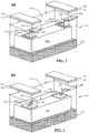
FIG. 1A is a partially exploded isometric view of a leadframe-less surface mount semiconductor device in accordance with a first embodiment of the present invention, andFIGS. 1B and 1C are cross-sectional side views of the device ofFIG. 1A from sides A and B; -
FIG. 2 is a partially exploded isometric view of a leadframe-less surface mount semiconductor device in accordance with a second embodiment of the present invention; -
FIG. 3 is a partially exploded isometric view of a leadframe-less surface mount semiconductor device in accordance with a third embodiment of the present invention; and -
FIGS. 4A-4B ,5A-5B ,6A-6B ,7-8 ,9A-9B, 10 ,11A-11B and12-13 are a series of diagrams illustrating steps in assembling a leadframe-less surface mount semiconductor in accordance with an embodiment of the present invention. - The detailed description set forth below in connection with the appended drawings is intended as a description of presently preferred embodiments of the invention, and is not intended to represent the only forms in which the present invention may be practised. It is to be understood that the same or equivalent functions may be accomplished by different embodiments that are intended to be encompassed within the spirit and scope of the invention. In the drawings, like numerals are used to indicate like elements throughout. It also should be noted that the drawings provide enlarged views and may not be drawn to scale so that particular features of the invention may be better understood. The terms "comprises," "comprising," or any variations thereof, are intended to cover a non-exclusive inclusion, such that module, circuit, device components, structures and method steps that comprises a list of elements or steps does not include only those elements but may include other elements or steps not expressly listed or inherent to such module, circuit, device components or steps. An element or step proceeded by "comprises ... a" does not, without more constraints, preclude the existence of additional identical elements or steps that comprises the element or step.
- In one embodiment, the present invention provides a semiconductor device including a semiconductor die having a top surface with one or more bond pads formed thereon, and one or more electrical connection elements each having a first end located at a first plane and electrically connected to one of the bond pads, and an opposite second end located at a second plane that is different from the first plane. A molding material encapsulates the semiconductor die and the electrical connection elements. The molding material defines a package body that has a top surface and one or more side surfaces. The second end of each electrical connection element is exposed at the top surface and at least one of the side surfaces of the package body.
- In another embodiment, the present invention provides a method for assembling a semiconductor device. The method includes providing a wafer that has a top surface and an opposite bottom surface, a plurality of semiconductor dies arranged in an array that extends in first and second directions, and saw streets located between adjacent ones of the semiconductor dies. Each semiconductor die has one or more bond pads formed on the top surface. The method also includes bonding one or more electrical connection elements to the bond pads of the semiconductor dies, wherein each electrical connection element bridges adjacent semiconductor dies in at least one of the first and second directions, and encapsulating the semiconductor dies and the electrical connection elements with a molding material to form an assembly of an array of semiconductor devices. Each semiconductor device comprises a package body formed by the molding material, and each of the one or more electrical connection elements has a bridge portion exposed at a top surface of the assembly. The method further includes singulating the semiconductor devices by cutting the assembly along the saw streets, wherein a remaining portion of each electrical connection element of each semiconductor device has an end exposed at a top surface and at least one side surface of the package body.
- Referring now to
FIGS. 1A-1C , an example of a leadframe-less surfacemount semiconductor device 100 is shown. In particular,FIG. 1A shows a partially exploded isometric view of the leadframe-less surfacemount semiconductor device 100, andFIGS. 1B and 1C are cross-sectional side views of the leadframe-less surface mount semiconductor device ofFIG. 1A from sides A and B. Thesemiconductor device 100 includes asemiconductor die 102 having a top surface with one ormore bond pads 104 formed thereon, and one or moreelectrical connection elements 106 each having afirst end 108 located at a first plane and electrically connected to one of the one ormore bond pads 104, and an oppositesecond end 110 located at a second plane that is different from the first plane. - In a preferred embodiment, the
first end 108 of theelectrical connection element 106 is bonded directly to thebond pad 104. In another preferred embodiment, thesemiconductor device 100 includes anoptional redistribution layer 112 located between thebond pad 104 and thefirst end 108 of theelectrical connection element 106. - The
semiconductor device 100 further includes amolding material 114 that covers or encapsulates thesemiconductor die 102 and the one or moreelectrical connection elements 104. Themolding material 114 defines apackage body 116 that has a top surface and one or more side surfaces. Thesecond end 110 of eachelectrical connection element 106 is exposed at the top surface and at least one of the one or more side surfaces of thepackage body 116. In a preferred embodiment, theelectrical connection element 106 is a conductive clip formed from copper that may be plated or unplated. Thesecond end 110 of eachelectrical connection element 106 is exposed at the top surface and two adjacent side surfaces of thepackage body 116. - In a preferred embodiment, the
semiconductor device 100 includes ametal layer 118 formed over the top surface of thepackage body 116 and electrically connected to thesecond end 110 of eachelectrical connection element 106. In a preferred embodiment, themetal layer 118 comprises copper or another conductive metal. In another preferred embodiment, themetal layer 118 is coated with awettable material 120, such as tin, using an electrically conductive plating process. - In a preferred embodiment, the
semiconductor device 100 further includes adie carrier 122, wherein a bottom surface of the semiconductor die 102 is attached to the diecarrier 122 with an adhesive material. In a preferred embodiment, the diecarrier 122 is a substrate. In another preferred embodiment, the diecarrier 122 is a tape. -
FIG. 2 is a partially exploded isometric view of a leadframe-less surfacemount semiconductor device 200 in accordance with a second embodiment of the present invention. Thesemiconductor device 200 is substantially the same as thesemiconductor device 100 except that theelectrical connection element 202 is a ribbon-shaped conductive metal clip that has asecond end 206 exposed at the top surface of thepackage body 116 and one side surface of thepackage body 116. -
FIG. 3 is a partially exploded isometric view of a leadframe-less surfacemount semiconductor device 300 in accordance with a third embodiment of the present invention. Thesemiconductor device 300 is substantially the same as thesemiconductor device 200 except that theelectrical connection element 302 comprises one or more bond wires that havesecond ends 306 exposed at the top surface of thepackage body 116 and one side surface of thepackage body 116. -
FIGS. 4A-4B ,5A-5B ,6A-6B ,7-8 ,9A-9B, 10 ,11A-11B and12-13 are a series of diagrams illustrating steps in assembling a leadframe-less surface mount semiconductor device in accordance with another embodiment of the present invention. - Starting with
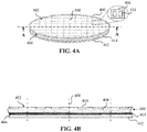
FIGS. 4A and 4B , awafer 400 that has atop surface 402 and anopposite bottom surface 404 is provided.FIG. 4A is an isometric view of thewafer 400 andFIG. 4B is a cross-sectional side view of thewafer 400 along line A-A ofFIG. 4A . Thewafer 400 comprises a plurality of semiconductor dies 406 and has sawstreets 408 located between adjacent ones of the dies 406. Each die 406 has one ormore bond pads 410 formed on thetop surface 402. In a preferred embodiment, each die 400 comprises one or more active components (i.e., internal circuitry not shown) such as transistors or diodes, and thebond pads 410 preferably are formed by depositing a patterned metal layer on thetop surface 402. Thebond pads 410 provide electrical connections to the active components within thedie 406. In a preferred embodiment, thebottom surface 404 of thewafer 400 is mounted on a top surface of acarrier 412 with anadhesive material 414. In a preferred embodiment, thecarrier 412 is a semiconductor substrate. - In the next step, illustrated in
FIGS. 5A and 5B , thewafer 400 is cut along thesaw streets 408 to form a plurality oftrenches 418 between adjacent ones of the dies 406.FIG. 5A is a top plan view of thewafer 400 after the cut, andFIG. 5B is a cross-sectional side view of aportion 500 of thewafer 400 along the line B-B ofFIG. 5A . As shown inFIG. 5A , the semiconductor dies 406 are arranged in an array extending in both X and Y directions. In a preferred embodiment, thetrenches 418 extend down to theadhesive material 414. In another preferred embodiment, thetrenches 418 extend beyond theadhesive material 414 and into thecarrier 412. - In the next step, illustrated in
FIGS. 6A and 6B , a plurality ofelectrical connection elements 502 are attached or electrically connected to thebond pads 410 of the semiconductor dies 406. Theelectrical connection elements 502 includefeet 508, and eachelectrical connection element 502 bridges adjacent semiconductor dies 406 in at least one of the X and Y directions.FIG. 6A is a top plan view of thewafer 400 with theelectrical connection elements 502 bonded thereto, andFIG. 6B is an enlarged isometric view of aportion 504 of the semiconductor dies 406 and theelectrical connection elements 502 that include four semiconductor dies 406 adjacent to an intersection of twoperpendicular trenches 418. - In a preferred embodiment, redistribution layers 506 are attached to the
bond pads 410, and theelectrical connection elements 502 are bonded to the redistribution layers 506 and electrically connected to thebond pads 410 through the redistribution layers 506. The redistribution layers 506 are provided as an option if thebond pad 410 does not have enough area to cater for thefeet 508 of theelectrical connection elements 502. In a preferred embodiment, the redistribution layers 506 are separate pieces respectively located between thebond pads 410 and thefeet 508 of theelectrical connection elements 502. In another preferred embodiment, there is asingle redistribution layer 506 located over the top surface of the semiconductor die 406. - In a preferred embodiment as shown in
FIGS. 6A and 6B , theelectrical connection element 502 comprises a metal gang clip that has fourfeet 508 respectively bonded tobond pads 410 of four semiconductor dies 406 adjacent to an intersection of twoperpendicular trenches 418, and abridge portion 510 connecting the fourfeet 504, such that theelectrical connection elements 502 bridge adjacent semiconductor dies 406 in both the X and Y directions. - In another preferred embodiment as shown in
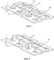
FIG. 7 , theelectrical connection element 502 is a ribbon-shaped metal clip that has twofeet 508 bonded to bond pads of two adjacent semiconductor dies 406, and thebridge portion 510 connecting the twofeet 508, such thatelectrical connection element 502 bridges the two adjacent semiconductor dies 406 in the Y direction. - In yet another embodiment as shown in
FIG. 8 , theelectrical connection elements 502 comprises bond wires that bridge adjacent semiconductor dies 406 in the Y direction. - In the next step, illustrated in
FIGS. 9A and 9B , the semiconductor dies 406 and theelectrical connection elements 502 are encapsulated with amolding material 512 to form anassembly 514 of an array ofsemiconductor devices 516 separated by sawstreets 518.FIGS. 9A and 9B are respectively a cross-sectional side view and a top plan view of theassembly 514. Themolding material 512 fills the plurality oftrenches 418 and covers side surfaces of the semiconductor dies 406. Eachsemiconductor device 516 comprises apackage body 520 formed by themolding material 512, wherein thebridge portion 510 of theelectrical connection elements 502 is exposed at a top surface of theassembly 514. - In the next step, illustrated in
FIG. 10 , ametal layer 522 is formed over the top surface of theassembly 514. In a preferred embodiment, themetal layer 522 is formed by sputtering or plating. In a preferred embodiment, themetal layer 522 comprises copper. - As shown in
FIGS. 11A and11B ,openings 524 are selectively formed within themetal layer 522 by chemical etching or mechanical half-cutting to electrically isolate thebond pads 410 of each semiconductor die 406 from each other.FIGS. 11A and11B respectively show a cross-sectional side view and a top plan view of theassembly 514 after theopenings 524 have been formed in themetal layer 522. Themolding material 512 is exposed at theopenings 524. In a preferred embodiment, theopenings 524 are parallel to thesaw streets 518 in one direction. In another preferred embodiment, theopenings 524 do not extend to the edge of themetal layer 522, such that themetal layer 522 remains one piece of metal and is not split by any of theopenings 524. In a preferred embodiment, as shown inFIG. 12 , themetal layer 522 is coated with awettable material 526 such as by by electro-plating. Thewettable material 526 may comprise tin or a tin alloy, as is known in the art. In an alternate embodiment, the electro-plating is performed before theopenings 524 are formed. In the next step, illustrated inFIG. 13 , singulation is performed along thesaw streets 518 to separate thesemiconductor devices 516 from each other. After singulation, the remainingbridge portion 510 of theelectrical connection element 502 is exposed at a top surface and at least one side surface of thepackage body 520. - In an embodiment semiconductor device, may comprise: a die with at least two bond pads on a top surface thereof; at least two electrically conductive clips having first ends respectively connected to the bond pads; a molding material covering the die and the clips, wherein the mold compound forms a package body and opposite second ends of the clips are exposed at a top surface of the package body and at least one side surface of the package body; and at least two metal layers formed over respective exposed second ends of the clips and the top surface of the package body.
- The second ends of the clips may be exposed at the top surface of the package body and two adjacent side surfaces of the package body.
- The description of the preferred embodiments of the present invention has been presented for purposes of illustration and description, but is not intended to be exhaustive or to limit the invention to the forms disclosed. It will be appreciated by those skilled in the art that changes could be made to the embodiments described above without departing from the broad inventive concept thereof. It is understood, therefore, that this invention is not limited to the particular embodiment disclosed, but covers modifications within the spirit and scope of the present invention as defined by the appended claims.
Claims (15)
- A semiconductor device, comprising:a semiconductor die having a top surface with one or more bond pads formed thereon, and an opposite bottom surface;one or more electrical connection elements each having a first end located at a first plane and electrically connected to one of the one or more bond pads, and an opposite second end located at a second plane that is different from the first plane; anda molding material encapsulating the semiconductor die and the one or more electrical connection elements, wherein the molding material defines a package body that has a top surface and one or more side surfaces, wherein the second end of each electrical connection element is exposed at the top surface and at least one of the one or more side surfaces of the package body.
- The semiconductor device of claim 1, wherein the second end of each of the one or more electrical connection elements is exposed at the top surface and two adjacent side surfaces of the package body.
- The semiconductor device of claim 1 or 2, further comprising:a metal layer formed over the top surface of the package body and electrically connected to at least one of the one or more electrical connection elements.
- The semiconductor device of claim 3, wherein the metal layer is coated with a wettable material by electrically conductive plating.
- The semiconductor device of any of claims 1 to 4, further comprising:a die carrier, wherein the bottom surface of the semiconductor die is attached to the die carrier; and/ora redistribution layer located between the one or more bond pads and the one or more electrical connection elements.
- The semiconductor device of any of claims 1 to 5, wherein the one or more electrical connection elements are metal clips; and/or bond wires.
- A method for assembling a semiconductor device, the method comprising:providing a wafer that has a top surface and an opposite bottom surface, wherein the wafer comprises a plurality of semiconductor dies arranged in an array that extends in first and second directions, and saw streets located between adjacent ones of the semiconductor dies, wherein each semiconductor die has one or more bond pads formed on the top surface;bonding one or more electrical connection elements to the bond pads of the semiconductor dies, wherein each electrical connection element bridges adjacent semiconductor dies in at least one of the first and second directions;encapsulating the semiconductor dies and the one or more electrical connection elements with a molding material to form an assembly of an array of semiconductor devices, wherein each semiconductor device comprises a package body formed by the molding material, and each of the one or more electrical connection elements has a bridge portion exposed at a top surface of the assembly; andsingulating the semiconductor devices by cutting the assembly along the saw streets, wherein a remaining portion of each electrical connection element of each semiconductor device has an end exposed at a top surface and at least one side surface of the package body.
- The method of claim 7, wherein each electrical connection element bridges adjacent semiconductor dies in both the first and second directions, such that the remaining portion of each electrical connection element of each semiconductor device has an end exposed at the top surface and two adjacent side surfaces of the package body.
- The method of any of claims 7 or 8, further comprising:cutting the wafer along the saw streets to form a plurality of trenches between adjacent ones of the dies before said encapsulating, such that after said encapsulating, the molding material fills the plurality of trenches and covers side surfaces of the semiconductor dies.
- The method of any of claims 7 to 9, further comprising:forming a metal layer over the top surface of the assembly; andselectively cutting the metal layer to electrically isolate the electrical connection elements of each semiconductor device from each other.
- The method of claim 14, wherein the metal layer is formed by sputtering or plating.
- The method of any of claims 10 or 11, further comprising:electro-plating the metal layer with a wettable material.
- The method of any of claims 7 to 12, further comprising:mounting the bottom surface of the wafer to a top surface of a carrier.
- The method of any of claims 7 to 13, further comprising:forming a redistribution layer over the top surface of the wafer before bonding the one or more electrical connection elements to the bond pads of the semiconductor dies.
- The method of any of claims 7 to 14, wherein the one or more electrical connection elements are metal clips, wherein each metal clip has four feet respectively electrically connected to bond pads of semiconductor dies located at four quarters of an intersection of two saw streets, and a bridge portion connecting the four feet, and/or wherein the one or more electrical connection elements are bond wires.
Applications Claiming Priority (1)
| Application Number | Priority Date | Filing Date | Title |
|---|---|---|---|
| US15/287,584 US20180102287A1 (en) | 2016-10-06 | 2016-10-06 | Leadframe-less surface mount semiconductor device |
Publications (2)
| Publication Number | Publication Date |
|---|---|
| EP3306660A2 true EP3306660A2 (en) | 2018-04-11 |
| EP3306660A3 EP3306660A3 (en) | 2018-06-27 |
Family
ID=59520833
Family Applications (1)
| Application Number | Title | Priority Date | Filing Date |
|---|---|---|---|
| EP17184584.5A Withdrawn EP3306660A3 (en) | 2016-10-06 | 2017-08-02 | Leadframe-less surface mount semiconductor device |
Country Status (3)
| Country | Link |
|---|---|
| US (1) | US20180102287A1 (en) |
| EP (1) | EP3306660A3 (en) |
| CN (1) | CN107919331A (en) |
Cited By (5)
| Publication number | Priority date | Publication date | Assignee | Title |
|---|---|---|---|---|
| CN114597170A (en) * | 2020-12-04 | 2022-06-07 | 芯沣科技有限公司 | Semiconductor element package structure and manufacturing method thereof |
| US11393699B2 (en) | 2019-12-24 | 2022-07-19 | Vishay General Semiconductor, Llc | Packaging process for plating with selective molding |
| US11450534B2 (en) | 2019-12-24 | 2022-09-20 | Vishay General Semiconductor, Llc | Packaging process for side-wall plating with a conductive film |
| US12211704B2 (en) | 2019-03-08 | 2025-01-28 | Siliconix Incorporated | Semiconductor package having side wall plating |
| US12224232B2 (en) | 2019-03-08 | 2025-02-11 | Siliconix Incorporated | Semiconductor package having side wall plating |
Families Citing this family (2)
| Publication number | Priority date | Publication date | Assignee | Title |
|---|---|---|---|---|
| US10879155B2 (en) * | 2019-05-09 | 2020-12-29 | Texas Instruments Incorporated | Electronic device with double-sided cooling |
| US11699640B2 (en) * | 2021-06-21 | 2023-07-11 | Infineon Technologies Ag | Power semiconductor module for PCB embedding, power electronic assembly having a power module embedded in a PCB, and corresponding methods of production |
Family Cites Families (5)
| Publication number | Priority date | Publication date | Assignee | Title |
|---|---|---|---|---|
| JP2725719B2 (en) * | 1994-11-21 | 1998-03-11 | 松下電子工業株式会社 | Electronic component and method of manufacturing the same |
| JPH11162998A (en) * | 1997-11-28 | 1999-06-18 | Mitsubishi Electric Corp | Semiconductor device and manufacturing method thereof |
| US20050151268A1 (en) * | 2004-01-08 | 2005-07-14 | Boyd William D. | Wafer-level assembly method for chip-size devices having flipped chips |
| ITMI20130473A1 (en) * | 2013-03-28 | 2014-09-29 | St Microelectronics Srl | METHOD FOR MANUFACTURING ELECTRONIC DEVICES |
| US9837368B2 (en) * | 2014-03-04 | 2017-12-05 | Maxim Integrated Products, Inc. | Enhanced board level reliability for wafer level packages |
-
2016
- 2016-10-06 US US15/287,584 patent/US20180102287A1/en not_active Abandoned
-
2017
- 2017-08-02 EP EP17184584.5A patent/EP3306660A3/en not_active Withdrawn
- 2017-09-29 CN CN201710912158.XA patent/CN107919331A/en active Pending
Non-Patent Citations (1)
| Title |
|---|
| None |
Cited By (7)
| Publication number | Priority date | Publication date | Assignee | Title |
|---|---|---|---|---|
| US12211704B2 (en) | 2019-03-08 | 2025-01-28 | Siliconix Incorporated | Semiconductor package having side wall plating |
| US12224232B2 (en) | 2019-03-08 | 2025-02-11 | Siliconix Incorporated | Semiconductor package having side wall plating |
| US11393699B2 (en) | 2019-12-24 | 2022-07-19 | Vishay General Semiconductor, Llc | Packaging process for plating with selective molding |
| US11450534B2 (en) | 2019-12-24 | 2022-09-20 | Vishay General Semiconductor, Llc | Packaging process for side-wall plating with a conductive film |
| US11764075B2 (en) | 2019-12-24 | 2023-09-19 | Vishay General Semiconductor, Llc | Package assembly for plating with selective molding |
| US11876003B2 (en) | 2019-12-24 | 2024-01-16 | Vishay General Semiconductor, Llc | Semiconductor package and packaging process for side-wall plating with a conductive film |
| CN114597170A (en) * | 2020-12-04 | 2022-06-07 | 芯沣科技有限公司 | Semiconductor element package structure and manufacturing method thereof |
Also Published As
| Publication number | Publication date |
|---|---|
| CN107919331A (en) | 2018-04-17 |
| US20180102287A1 (en) | 2018-04-12 |
| EP3306660A3 (en) | 2018-06-27 |
Similar Documents
| Publication | Publication Date | Title |
|---|---|---|
| US12094725B2 (en) | Leadframe package with pre-applied filler material | |
| US20180102287A1 (en) | Leadframe-less surface mount semiconductor device | |
| US11049843B2 (en) | Semiconductor packages | |
| CN101512762B (en) | Stackable packages for three-dimensional packaging of semiconductor dice | |
| CN102789994B (en) | The wettable semiconductor device in side | |
| US10930581B2 (en) | Semiconductor package with wettable flank | |
| US7671451B2 (en) | Semiconductor package having double layer leadframe | |
| TWI495055B (en) | Semiconductor chip package and method of manufacturing same | |
| US20050029640A1 (en) | Semiconductor device and method of manufacturing thereof | |
| US9478517B2 (en) | Electronic device package structure and method of fabricating the same | |
| US8115288B2 (en) | Lead frame for semiconductor device | |
| US20090065915A1 (en) | Singulated semiconductor package | |
| US9842794B2 (en) | Semiconductor package with integrated heatsink | |
| US10090228B1 (en) | Semiconductor device with leadframe configured to facilitate reduced burr formation | |
| US9978695B1 (en) | Semiconductor device including leadframe with a combination of leads and lands and method | |
| KR20180105550A (en) | Method of forming a packaged semiconductor device using ganged conductive connective assembly and structure | |
| US20150035166A1 (en) | Method for manufacturing a semiconductor component and structure | |
| US9508631B1 (en) | Semiconductor device including leadframe with a combination of leads and lands and method | |
| US11721654B2 (en) | Ultra-thin multichip power devices | |
| CN108074901B (en) | Semiconductor device with wettable corner leads and semiconductor device assembly method | |
| CN102468194A (en) | Semiconductor device packaging method and semiconductor device package | |
| US9935030B2 (en) | Resin-encapsulated semiconductor device | |
| US20190355651A1 (en) | Two sided bondable lead frame | |
| KR20120018756A (en) | Leadframe for ic package and method of manufacture | |
| CN119447068A (en) | Semiconductor device and manufacturing method |
Legal Events
| Date | Code | Title | Description |
|---|---|---|---|
| PUAI | Public reference made under article 153(3) epc to a published international application that has entered the european phase |
Free format text: ORIGINAL CODE: 0009012 |
|
| AK | Designated contracting states |
Kind code of ref document: A2 Designated state(s): AL AT BE BG CH CY CZ DE DK EE ES FI FR GB GR HR HU IE IS IT LI LT LU LV MC MK MT NL NO PL PT RO RS SE SI SK SM TR |
|
| AX | Request for extension of the european patent |
Extension state: BA ME |
|
| PUAL | Search report despatched |
Free format text: ORIGINAL CODE: 0009013 |
|
| AK | Designated contracting states |
Kind code of ref document: A3 Designated state(s): AL AT BE BG CH CY CZ DE DK EE ES FI FR GB GR HR HU IE IS IT LI LT LU LV MC MK MT NL NO PL PT RO RS SE SI SK SM TR |
|
| AX | Request for extension of the european patent |
Extension state: BA ME |
|
| RIC1 | Information provided on ipc code assigned before grant |
Ipc: H01L 23/31 20060101ALI20180523BHEP Ipc: H01L 23/495 20060101AFI20180523BHEP |
|
| STAA | Information on the status of an ep patent application or granted ep patent |
Free format text: STATUS: THE APPLICATION IS DEEMED TO BE WITHDRAWN |
|
| 18D | Application deemed to be withdrawn |
Effective date: 20190103 |