EP3304312B1 - Post-silicon validation and debug using symbolic quick error detection - Google Patents
Post-silicon validation and debug using symbolic quick error detection Download PDFInfo
- Publication number
- EP3304312B1 EP3304312B1 EP16808080.2A EP16808080A EP3304312B1 EP 3304312 B1 EP3304312 B1 EP 3304312B1 EP 16808080 A EP16808080 A EP 16808080A EP 3304312 B1 EP3304312 B1 EP 3304312B1
- Authority
- EP
- European Patent Office
- Prior art keywords
- qed
- bug
- instructions
- symbolic
- bmc
- Prior art date
- Legal status (The legal status is an assumption and is not a legal conclusion. Google has not performed a legal analysis and makes no representation as to the accuracy of the status listed.)
- Active
Links
Images







Classifications
-
- G—PHYSICS
- G06—COMPUTING OR CALCULATING; COUNTING
- G06F—ELECTRIC DIGITAL DATA PROCESSING
- G06F11/00—Error detection; Error correction; Monitoring
- G06F11/30—Monitoring
- G06F11/34—Recording or statistical evaluation of computer activity, e.g. of down time, of input/output operation ; Recording or statistical evaluation of user activity, e.g. usability assessment
- G06F11/3466—Performance evaluation by tracing or monitoring
-
- G—PHYSICS
- G06—COMPUTING OR CALCULATING; COUNTING
- G06F—ELECTRIC DIGITAL DATA PROCESSING
- G06F11/00—Error detection; Error correction; Monitoring
- G06F11/22—Detection or location of defective computer hardware by testing during standby operation or during idle time, e.g. start-up testing
- G06F11/2205—Detection or location of defective computer hardware by testing during standby operation or during idle time, e.g. start-up testing using arrangements specific to the hardware being tested
- G06F11/2236—Detection or location of defective computer hardware by testing during standby operation or during idle time, e.g. start-up testing using arrangements specific to the hardware being tested to test CPU or processors
-
- G—PHYSICS
- G06—COMPUTING OR CALCULATING; COUNTING
- G06F—ELECTRIC DIGITAL DATA PROCESSING
- G06F11/00—Error detection; Error correction; Monitoring
- G06F11/30—Monitoring
- G06F11/3003—Monitoring arrangements specially adapted to the computing system or computing system component being monitored
-
- G—PHYSICS
- G06—COMPUTING OR CALCULATING; COUNTING
- G06F—ELECTRIC DIGITAL DATA PROCESSING
- G06F11/00—Error detection; Error correction; Monitoring
- G06F11/30—Monitoring
- G06F11/3003—Monitoring arrangements specially adapted to the computing system or computing system component being monitored
- G06F11/3024—Monitoring arrangements specially adapted to the computing system or computing system component being monitored where the computing system component is a central processing unit [CPU]
-
- G—PHYSICS
- G06—COMPUTING OR CALCULATING; COUNTING
- G06F—ELECTRIC DIGITAL DATA PROCESSING
- G06F11/00—Error detection; Error correction; Monitoring
- G06F11/30—Monitoring
- G06F11/3065—Monitoring arrangements determined by the means or processing involved in reporting the monitored data
- G06F11/3072—Monitoring arrangements determined by the means or processing involved in reporting the monitored data where the reporting involves data filtering, e.g. pattern matching, time or event triggered, adaptive or policy-based reporting
- G06F11/3079—Monitoring arrangements determined by the means or processing involved in reporting the monitored data where the reporting involves data filtering, e.g. pattern matching, time or event triggered, adaptive or policy-based reporting the data filtering being achieved by reporting only the changes of the monitored data
Definitions
- This disclosure relates generally to integrated circuits (ICs) and more particularly to methods and structures for effective post-silicon validation and debug of integrated circuits including systems-on-a-chip (SoC).
- ICs integrated circuits
- SoC systems-on-a-chip
- An advance in the art is made according to an aspect of the present disclosure directed to improved methods and structures for verifying, validating and debugging integrated circuits and systems-on-a-chip constructed therefrom.
- Symbolic Quick Error Detection or Symbolic QED Symbolic Quick Error Detection or Symbolic QED.
- Illustrative characteristics of Symbolic QED include: 1) It is applicable to any System-on-Chip (SoC) design as long as it contains at least one programmable processor (a generally valid assumption for existing SoCs); 2) It is broadly applicable for logic bugs inside processor cores, accelerators, and uncore components; 3) It does not require failure reproduction; 4) It does not require human intervention during bug localization; 5) It does not require trace buffers; 6) It does not require assertions; and 7) It uses hardware structures called "change detectors" which introduce only a small area overhead
- Symbolic QED relies on the following steps that work together in a coordinated fashion: 1) A systematic (and automated) approach to inserting "change detectors" during a design phase; 2) Quick Error Detection (QED) tests that detect bugs with short error detection latencies and high coverage; and 3)Formal techniques that enable bug localization and generation of minimal bug traces upon bug detection.
- any element expressed as a means for performing a specified function is intended to encompass any way of performing that function including, for example, a) a combination of circuit elements which performs that function or b) software in any form, including, therefore, firmware, microcode or the like, combined with appropriate circuitry for executing that software to perform the function.
- the invention as defined by such claims resides in the fact that the functionalities provided by the various recited means are combined and brought together in the manner which the claims call for. Applicant thus regards any means which can provide those functionalities as equivalent as those shown herein.
- QED Quick Error Detection
- Electrical Bugs - are a type of bug that only manifests itself under specific operating conditions (voltage, frequency, temperature, etc.) and may be caused by design marginalities, synchronization problems, noise, etc.
- Logic bugs - are a type of bug that is caused by one or more design error(s). Logic bugs include incorrect hardware implementations or incorrect interactions between the hardware implementation and low-level system software (e.g., firmware).
- SoC System on a Chip
- IC integrated circuit
- SoC may contain digital, analog, mixed-signal, and radio frequency functions.
- SoC may also refer to technology(ies) that package or otherwise integrate all parts for a system on a single integrated circuit.
- Uncore - are components in a SoC that are neither processor cores nor ⁇ processors (e.g., graphical processing tmits). Examples of uncore components include cache controllers, memory controllers, and interconnection network.
- post-silicon validation and debug of integrated circuits has become a critically important step with respect to their design, test, manufacture and support.
- post-silicon validation and debug is the last step in the development of a semiconductor IC and occurs between pre-silicon verification and high volume manufacturing.
- post-silicon verification, validation and debug is contrasted with pre-silicon verification or debug processes, wherein during pre-silicon process(es), devices are generally tested in a virtual environment with sophisticated simulation, emulation and cformal verification tools.
- pre-silicon verification processes alone are inadequate for verifying correct operation of contemporary ICs and in particular SoCs.
- such traditional, prior art pre-silicon techniques are generally too slow and do not adequately address electrical bugs. Consequently, there is growing reliance by those skilled in the art on system-level validation (i.e., emulation) and post-silicon validation (PSV) techniques.
- system-level validation i.e., emulation
- PSV post-silicon validation
- post-silicon validation and debug of an IC involves three activities namely:
- post-silicon bug localization involves identifying a sequence of inputs (e.g., instructions) that activate and detect the bug (also referred to as a bug trace), and any physical hardware (design block) where the bug is (possibly) located.
- post-silicon bug localization is particularly difficult because many existing post-silicon techniques rely on: 1) system, level simulation to obtain expected or "golden” system response; and/or 2) failure reproduction - which involves returning the system to an error-free state and rerunning the system with the exact input stimuli (e.g., validation test instructions; validation test inputs; voltage, temperature, and frequency operation conditions; and interrupts) - to reproduce the failure.
- input stimuli e.g., validation test instructions; validation test inputs; voltage, temperature, and frequency operation conditions; and interrupts
- Symbolic Quick Error Detection or Symbolic QED Symbolic Quick Error Detection or Symbolic QED.
- Illustrative characteristics of Symbolic QED include: 1) It is applicable to any System-on-Chip (SoC) design as long as it contains at least one programmable processor (a generally valid assumption for existing SoCs); 2) It is broadly applicable for logic bugs inside processor cores, accelerators, and uncore components; 3) It does not require failure reproduction; 4) It does not require human intervention during bug localization; 5) It does not require trace buffers; 6) It does not require assertions; and 7) It uses hardware structures called "change detectors" which introduce only a small area overhead (1.86% on OpenSPARC).
- SoC System-on-Chip
- Symbolic QED employs the following methodologies which advantageously work together in a coordinated fashion namely, 1) A systematic (and automated) approach to inserting "change detectors" during design phase(s); 2) Quick Error Detection (QED) tests that detect bugs exhibiting short error detection latencies and high coverage; and 3) Formal techniques that enable bug localization and generation of minimal bug traces upon bug detection.
- Symbolic QED involves two distinct phases namely, a design phase and a post-silicon validation phase. As depicted in that figure, the design phase systematically and automatically inserts change detectors inside a design.
- the post-silicon validation phase involves running QED tests wherein change detectors record debug information and if errors are detected then localizing bug(s) and producing bug trace reports by formal analysis.
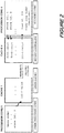
- the bug is only activated when two store operations occur within 2 clock cycles of each other to adjacent cache lines.
- the next cache coherence message (e.g., invalidation) is delayed because of a delay in the receive buffer of the cache (these details were not known before the bug was found and localized).
- a test running on the SoC created a deadlock.
- the deadlock occurs because one of the processor cores (core 4) performs a store to memory location [A] followed by a store to memory location [B] within 2 clock cycles ([A] and [B] are cached on adjacent cache lines).
- the example bug scenario is activated in cache 4.
- processor core 1 After the bug is activated, processor core 1 performs a store to memory location [C]. Since memory location [C] is cached in multiple caches (cache 1 and cache 4), the store operation to memory location [C] has to invalidate other cached copies of memory location [C] (including the cached copy in cache 4). However, due to the bug, an invalidation message received by cache 4 is delayed by 5 clock cycles.
- processor core 4 loads from memory location [C]. Since the cached copy of memory location [C] in cache 4 is still marked as valid, it loads this stale copy (which contains the wrong value at this point). Then, millions of clock cycles later, processor core 4 uses the wrong value of memory location [C] in code that performs locking, resulting in deadlock.
- the bug When deadlocks such as this are detected (e.g., by using a timeout), the bug must be localized by identifying the bug trace and the component where the bug is located. Since it is not known a priori when the bug was activated or when the system entered deadlock, it can be very difficult to obtain the bug trace.
- the bug trace can be extremely long due to the long error detection latency, containing many extraneous instructions unnecessary for activating or detecting the bug.
- such bugs can be extremely challenging to localize using traditional approaches like failure reproduction, trace buffers, simulation, or na ⁇ ve formal methods.
- QED Quick Error Detection
- the software-only QED technique automatically transforms existing post-silicon validation tests (original tests) into new QED tests using various QED transformations e.g., Error detection using Duplicated Instructions for Validation ( EDDI-V ) and Proactive Load and Check ( PLC ) .
- EDDI-V - EDDI-V targets processor core bugs by frequently checking results of original instructions against results of duplicated instructions created by EDDI-V.
- registers and memory space are divided into two halves, one for original instructions and one for duplicated instructions.
- corresponding registers and memory locations for the original and the duplicated instructions are initialized to the same values.
- EDDI-V creates a corresponding duplicate instruction that performs the same operation - but only for registers and memory reserved for duplicate instructions.
- the duplicated instructions execute in the same order as original instructions.
- the EDDI-V transformation also inserts periodic check instructions (called Normal checks ) that compare the results of the original instructions against those of the duplicated instructions.
- an additional Load check instruction is inserted immediately after (before the loaded values are used by any other instructions) to check that the value loaded by the original instruction matches the value loaded by the corresponding duplicated instruction.
- a Store check instruction is inserted immediately before the original store instruction to check that the value about to be stored matches the value about to be stored by the duplicated instruction.
- Each check instruction is of the form: CMP ⁇ Ra , Ra ′ where Ra and Ra' are an original and (corresponding) duplicate register respectively. A mismatch in any check instruction indicates an error.
- insertion of the duplicated instructions and the check instructions is controlled by parameters Inst_min and Inst_max, the minimum and maximum number of instructions from the original test that must execute before any duplicated or check instructions execute.
- PLC - PLC targets bugs inside uncore components by frequently and proactively performing loads from memory (through uncore components) and checking the values loaded.
- PLC first transforms an original test into an EDDI-V-transformed QED test.
- PLC inserts Proactive Load and Check (PLC) operations throughout the transformed test. PLC operations run on all cores and all threads.
- PLC Proactive Load and Check
- Each PLC operation iterates through all the variables selected for PLC check as follows:
- Symbolic QED - As we shall show and describe, Symbolic QED localizes bugs and automatically produces short bug traces that typically have only a few instructions (often less than 10). Within the space of QED-compatible bug traces (explained below), the traces produced by Symbolic QED are minimal, meaning no shorter bug traces exist. As will be readily understood and greatly appreciated by those skilled in the art, short bug traces - such as those produced by Symbolic QED - make bugs easier to understand and fix.
- Symbolic QED employs bounded model checking (BMC) used in formal verification.
- BMC bounded model checking
- BMC guarantees that if a property can be violated, a minimal-length counter-example is returned.
- BMC needs a property to solve for. Since bugs are not known a priori, it is difficult to craft such properties (and avoid false positives). Second, large design sizes limit the effectiveness of BMC. If a design is too large, a typical BMC tool may not even be able to load the design. And even if a large design can be loaded, running BMC on that design will - in all likelihood - be very slow - may be unworkably so. Third, the performance of BMC techniques is affected by the number of cycles required to trigger a bug. More particularly, as the number of cycles required to trigger the bug increases, BMC performance slows down, especially for large designs. Thus, unless a short counter-example exists, BMC will take too long or may be unable to find it at all.
- the QED module only needs to be designed once for a given ISA, and made available as a "library component" for use during validation.
- the design of a QED module is simple, and can be tested in only a few minutes.
- the QED module automatically transforms a sequence of original instructions into a QED-compatible sequence. Any control-flow altering instruction determines the end of the "sequence of original instructions."
- the QED module only requires that the sequence is in fact made up of valid instructions and that they read from or write to only the registers and memory allocated for the original instructions (conditions that can be specified directly to the BMC tool).
- the sequence of original instructions is first executed unmodified (up to but not including the control-flow instruction). Then it is executed a second time - but instead of using the original registers and memory, the instructions are modified to use the registers and memory allocated for the duplicated instructions.
- the QED module Since duplication is triggered only by a control-flow instruction, the QED module does not use a fixed value for Inst _ min and Inst_max.
- the values are dynamically determined by the length of the sequence of original instructions. This makes it easy for the BMC tool to implicitly (and simultaneously ) search through all sequences of instructions and all values of Inst_min and Inst_max.
- FIGURE 3 shows how the QED module integrates with a fetch unit.
- the pseudo code of the QED module is shown in FIGURE 4 .
- the inputs to the QED module are: 1) enable, which disables the QED module if 0; 2) instruction_in, which is the instruction from the fetch unit to be executed by the processor core; 3) target_address, which contains the address of the next instruction to execute when the processor executes a control-flow instruction; and 4) committed, which is a signal from the processor core to indicate if the instruction fetched has been committed (i.e., the result written to register or memory).
- outputs from the QED module are: 1) PC , which is the address of the next instruction to fetch; 2) PC_override , which determines if the processor core should use the PC from the QED module or the PC from the fetch unit; 3) instruction out, which is the modified instruction computed by the QED module; 4) instruction_override, which determines whether the processor core should use the modified instruction from the QED module or the instruction from the fetch unit; and 5) qed_ready, which is set to qed_ready_i if the committed input signal is true, and false otherwise.
- the QED module has internal variables: 1) current _ mode, which tracks whether the QED module is executing original instructions ( ORIG_MODE ) or duplicated instructions ( DUP_MODE ); 2) qed _ rewind_address, which holds the address of the first instruction in the sequence of original instructions; 3) PC_override_i and instruction _ override _ i , which are internal versions of PC_override and instruction_ override (the only difference is that when the enable signal is set to 0, then both PC_override and instruction_override are also set to 0, disabling the QED module); and 5) qed_ready_i , which signals when both the original and duplicated registers should have the same values (under bug-free conditions). Initially, qed_ready_i is set to false, and is only set to true when both the original and duplicated instructions have executed.
- the QED module starts in ORIG_MODE.
- the QED module switches to DUP_MODE , loads the address stored in qed_rewind_address into PC, and sets PC_override_i to 1 (and as long as enable is true, PC_override is also set to 1).
- the processor core then re-executes instructions starting from the address stored in qed_rewind_address.
- the duplicated instruction is output as instruction out, and instruction override_i is set to 1 so the core executes the duplicated instruction instead of the original instruction from the fetch unit.
- instruction override_i is set to 1 so the core executes the duplicated instruction instead of the original instruction from the fetch unit.
- the corresponding registers should be equal, and so once the results are written to registers (the committed signal from the processor core is true), qed_ready is set to true.
- the processor will execute the control flow instruction and the QED module will store the address of the next instruction to execute (i.e., the target of the control flow instruction) in qed_rewind_address and then return to ORIG _ MODE .
- An example of the transformation performed by the QED module is shown in FIGURE 5 . More particularly, one can observe in FIGURE 5 , a sequence of original instructions and actual instructions executed.
- the approach outlined above ensures that only QED-compatible traces are considered by BMC.
- the initial state for the BMC run must be a QED-consistent state to ensure that no false counter-examples are generated. That is, the value of each register and memory location allocated for original instructions must match the corresponding register or memory location for duplicated instructions.
- One approach would be to start the processor from its reset state. However, the reset state may not be QED-consistent (or it may be difficult to confirm whether it is). Some designs also go through a reset sequence that may extend the number of cycles, making the BMC problem more difficult. For example, for OpenSPARC T2, only one processor core is active after a reset, and the system executes a sequence of initialization instructions (approximately 600 clock cycles long) to activate the other cores in the system.
- One way to obtain a QED-consistent state - according to the present disclosure - is to run "some" QED program (independent of specific tests for bug detection) in simulation and stop immediately after QED checks have compared all of the register and memory values (this ensures that each "original" register or memory location has the same value as its corresponding "duplicate” register or memory location).
- the register and memory values are read out of the simulator and used to set the register and memory values of the design when preparing to run BMC.
- ultrafast simulators not RTL
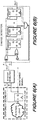
- FIGURE 6 shows a schematic diagram of a change detector according to an aspect of the present disclosure.
- change detectors to record changes in the logic values of signals during validation. These change detectors are inserted at the boundaries of all components that may potentially be removed in further analysis (e.g., at a certain level in the RTL hierarchy). For example, for our results shown and described later, change detectors were inserted on all signal lines one hierarchical level below the main SoC module of the OpenSPARC T2 design. They monitored signals between all modules at that level, which includes processor cores, L2 cache banks, memory controllers and I/O controllers.
- a change detector includes a k -bit ripple counter that is initialized to all 1's and is reset to all 0's whenever a change in signal values is detected. Due to the short error detection latencies of QED tests, k ⁇ 10 is generally sufficient ( change window of 1,023).
- k ⁇ 10 is generally sufficient ( change window of 1,023).
- Partial instantiation works through two design reduction techniques. The first technique takes all modules with multiple instantiations and repeatedly reduces their number by half until there is only 1 left. The second technique removes single-instance modules as long as removal of the module does not divide the design into two completely disconnected components.
- FIGURE 7 shows the steps for this approach. Once a full set of simplified (partially instantiated) designs is created, they are all analyzed using the BMC tool in parallel.
- the crossbar is not removed as it would disconnect the cores from the other components.
- the design reduces to 2 cores, 1 crossbar, 2 caches and 1 memory controller. This design does fit so we save it.
- the memory controller can be removed (since there is a single instance).
- the number of cores and caches can be divided by two. Both of these are saved. Further reductions result in smaller and smaller subsets of the design, each of which is saved. When no more reductions are possible, all of the saved designs are run in parallel.
- FIGURE 8 - which shows a schematic OpenSPARC T2 diagram - we now demonstrate the effectiveness of Symbolic QED using the OpenSPARC T2 SoC [OpenSPARC], which is the opensource version of the UltraSPARC T2, a 500-million-transistor SoC with 8 processor cores (64 hardware threads), a private L1 cache, 8 banks of shared L2 cache, 4 memory controllers, a crossbar-based interconnect, and various I/O controllers.
- OpenSPARC OpenSPARC
- the bug scenarios include bugs in the processor cores, bugs in the uncore components, and bugs related to power management.
- the activation criteron is set to a sequence of 5 instructions selected from the original test, executed on a designated processor core. This is to emulate a power management controller.
- the Questa Formal tool version 10.2c_3 from Mentor Graphics on an AMD Opteron 6438 with 128GB of RAM.
- the Inst_min and Inst_max QED transformation parameters were set to 100, which typically allow bugs to be detected within a few hundred clock cycles.
- the results are summarized in Table 1.
- the Original (No-QED) column shows results from running the original validation tests (FFT or MMULT) using end-result-checks to check the results of the test against pre-computed, known correct results.
- the QED column shows results from running the same tests after QED transformation. Note that unlike Symbolic QED, both the Original (No-QED) and the QED tests (without the analysis techniques discussed in Sec. III.E) are only able to report the existence of a bug; they cannot localize a bug (i.e., determine if the bug is in the processor core, in any of the uncore components, or is caused by interactions between the components), nor can they determine very precisely when a bug is activated.
- the table is categorized into processor core bugs, uncore bugs (here we include bugs that are inside uncore components as well as in the interface between processor cores and uncore components), and power management bugs. Each entry contains two sets of numbers, the top set contains the results obtained from the FFT test, and the bottom set contains results obtained from MMULT.
- “Bug trace length (instructions)” shows the [minimum, average, maximum] number of instructions in the bug trace.
- Busg trace length (cycles) represents the [minimum, average, maximum] number of clock cycles required to execute the bug trace.
- the two numbers are different because the Cycles Per Instruction (CPI) is not 1 for all instructions (for example, a load or store instruction may take multiple clock cycles to execute).
- the reported length for bug traces corresponds to the number of instructions in the trace found by the BMC tool (not including duplicated instructions created by the QED modules).
- the number of instructions for each core may be different. For example, one core could have a bug trace that is 3 instructions long, while another core has a bug trace that is 1 instruction long. We report the length of the longest bug trace for the cores (3 in this example) because all cores must complete to activate and detect the bug (and the cores execute the instructions in parallel).
- BMC runtime represents the [minimum, average, maximum] number of minutes it took for the BMC tool to find the bug traces.
- Bugs localized represents the percentage of bugs localized. Note that both Original (No-QED) and QED tests can only detect bugs, not localize bugs. We did not include any results from running the BMC without our Symbolic QED technique for two reasons: (i) the full design does not load into the BMC tool; and (ii) even if it did, we would need properties to check to run and there is no clear way to come up with such properties (other than manual insertion which would be subjective and extremely time-consuming).
- Change detectors determined that components such as the I/O controllers were not needed to activate the bugs.
- the partial instantiations involving the other components were run in parallel.
- the BMC runtime reported corresponds to the runtime of the smallest partial instantiation that produced a counter-example.
- this partial instantiation also provides us with a small candidate list of components that may contain the bug. For example, for a given bug, if both partial instances 2 and 5 produce a counter-example, then only the result from partial instance 5 is reported. This is because while both 2 and 5 contain processor cores and caches, 5 does not have a memory controller or a cache bank. This suggests that the memory controller and the cache bank are not required to activate and detect this bug.
- FIGURE 9 is a graph showing a breakdown of the bugs localized by Symbolic QED. Symbolic QED localized all 92 bug scenarios. For 26.1% of the bugs, Symbolic QED localized the bugs to exactly 1 processor core; for 56.5% of the bugs, Symbolic QED localized the bug to 1 processor core, 1 L2 cache bank and the crossbar that connects the two; and for 17.4% of the bugs, Symbolic QED localized the bug to 2 processor cores, 2 L2 cache banks, and the crossbar that connects the components.
- the BMC runtimes reported in Table 1 for Symbolic QED use the QED-consistent initial state constraint discussed previously.
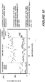
- FIGURE 10 Detailed runtimes for each bug are presented in FIGURE 10 .
- the runtime when starting from the state immediately after a reset sequence (which is QED-consistent in this case)
- the runtime when similarly seeding BMC after running MMULT demonstrate that using a QED-consistent initial state obtained by running a QED test achieves up to 5X improvement in runtime compared to starting from the state after reset. Note also that no significant differences were observed between the results from using the FFT test and those using the MMULT test.
- the overhead is significantly less than the 4% overhead of reconfigurable logic for post-silicon debugging. Furthermore, this approach avoids entirely the use of trace buffers (and the associated area overhead). And while we demonstrated the effectiveness of Symbolic QED on the OpenSPARC T2 SoC, Symbolic QED does not rely on any information about the specific implementation of the OpenSPARC T2. As a result, Symbolic QED is applicable to a wide variety of SoC designs.
- BackSpace and its derivatives provide a concrete bug trace once an error is detected or the system crashes by using formal methods to stitch together multiple short traces (or system states) into a longer trace.
- Some BackSpace derivatives require failure reproduction, which, as we discussed, is challenging due to Heisenbug effects.
- Other systems such as nuTAB-BackSpace, addresses some of the failure reproduction challenges but requires design-specific "rewrite rules" to determine if two similar states are equivalent. These rewrite rules have to be manually crafted by designers and require designer intuition, which may be difficult for large designs.
- the bug traces found may be very long, and unlike Symbolic QED, these techniques cannot reduce the length of the bug traces.
- techniques that solely rely on formal methods for bug localization are not scalable to large designs such as the OpenSPARC T2.
- FIGURE 10 shows an illustrative computer system 1000 suitable for implementing methods and systems according to an aspect of the present disclosure.
- a computer system may be integrated into an another system such as a router and may be implemented via discrete elements or one or more integrated components.
- the computer system may comprise, for example a computer running any of a number of operating systems.
- the above-described methods of the present disclosure may be implemented on the computer system 1000 as stored program control instructions.
- Computer system 1000 includes processor 1010, memory 1020, storage device 1030, and input/output structure 1040.
- One or more input/output devices may include a display 1045.
- One or more busses 1050 typically interconnect the components, 1010, 1020 , 1030, and 1040 .
- Processor 1010 may be a single or multi core. Additionally, the system may include accelerators etc further comprising the system on a chip.
- Processor 1010 executes instructions in which embodiments of the present disclosure may comprise steps described in one or more of the Drawing figures. Such instructions may be stored in memory 1020 or storage device 1030. Data and/or information may be received and output using one or more input/output devices.
- Memory 1020 may store data and may be a computer-readable medium, such as volatile or non-volatile memory.
- Storage device 1030 may provide storage for system 1000 including for example, the previously described methods.
- storage device 1030 may be a flash memory device, a disk drive, an optical disk device, or a tape device employing magnetic, optical, or other recording technologies.
- Input/output structures 1040 may provide input/output operations for system 1000 .
- Symbolic QED a structured and automated approach that overcomes post-silicon validation and debug challenges.
- Symbolic QED automatically detects and localizes logic bugs in post-silicon validation and provides a list of candidate components that may contain the bugs.
- Symbolic QED produces bug traces that are up to 6 orders of magnitude shorter than traditional post-silicon validation tests that rely on end-result-checks, and up to 5 orders of magnitude shorter than QED tests.
- Symbolic QED is completely automated, does not require human intervention, and does not need trace buffers.
Landscapes
- Engineering & Computer Science (AREA)
- Theoretical Computer Science (AREA)
- General Engineering & Computer Science (AREA)
- Physics & Mathematics (AREA)
- Quality & Reliability (AREA)
- General Physics & Mathematics (AREA)
- Computing Systems (AREA)
- Computer Hardware Design (AREA)
- Mathematical Physics (AREA)
- Computer Vision & Pattern Recognition (AREA)
- Debugging And Monitoring (AREA)
Description
- This disclosure relates generally to integrated circuits (ICs) and more particularly to methods and structures for effective post-silicon validation and debug of integrated circuits including systems-on-a-chip (SoC).
- As will be readily appreciated by those skilled in the art, the functionality and ubiquity of integrated circuits and systems constructed thereon has progressed at a breathtaking pace. Consequently, such circuits and systems have had a profound impact on contemporary society. Given their importance, methods and structures for the verification and/or validation of these circuits and systems would represent a welcome addition to the art.
- In an article entitled "Quick error detection tests with fast runtimes for effective post-silicon validation and debut", that appeardd in 2015 DESIGN, AUTOMATION & TEST IN EUROPE CONFERENCE AND EXIBITION, EDAA, 9 March 2015 (2015-03-09), pages 1168-1173, describe a technique called FAST QED (FastQED) that - according to the authors - overcomes drawbacks associated with software-only QED namely, increased post-silicon validation test runtimes. The Fast QED technique is claimed to exhibit fast runtimes, while simultaneously preserving short error detection latency and improved bug coverage benefit of software-only QED. Additionally, fast QED uses small hardware modifications to achieve fast runtimes.
- An advance in the art is made according to an aspect of the present disclosure directed to improved methods and structures for verifying, validating and debugging integrated circuits and systems-on-a-chip constructed therefrom.
- We call methods and structures according to the present disclosure Symbolic Quick Error Detection or Symbolic QED. Illustrative characteristics of Symbolic QED include: 1) It is applicable to any System-on-Chip (SoC) design as long as it contains at least one programmable processor (a generally valid assumption for existing SoCs); 2) It is broadly applicable for logic bugs inside processor cores, accelerators, and uncore components; 3) It does not require failure reproduction; 4) It does not require human intervention during bug localization; 5) It does not require trace buffers; 6) It does not require assertions; and 7) It uses hardware structures called "change detectors" which introduce only a small area overhead
- We demonstrate the effectiveness and practicality of Symbolic QED by showing that: 1) Symbolic QED correctly and automatically localizes difficult logic bugs in a few hours (less than 7 on OpenSPARC) that would take days or weeks to localize using traditional approaches; 2) For each detected bug, Symbolic QED provides a set of candidate components representing the possible locations of the bug in the design; 3) For each detected bug, Symbolic QED automatically generates a minimal bug trace using formal analysis; and 4) Symbolic QED generates bug traces that are up to 6 orders of magnitude shorter than those produced by traditional post-silicon techniques and 5 orders of magnitude shorter than QED.
- Symbolic QED relies on the following steps that work together in a coordinated fashion: 1) A systematic (and automated) approach to inserting "change detectors" during a design phase; 2) Quick Error Detection (QED) tests that detect bugs with short error detection latencies and high coverage; and 3)Formal techniques that enable bug localization and generation of minimal bug traces upon bug detection.
- In sharp contrast to prior-art methods, Symbolic QED automatically localizes logic bugs in SoCs during post-silicon validation and debug thus enabling extremely quick error detection and localization advantageously producing improved performance of both the debugging and the resulting systems along with significant productivity and time-to-market gains.
- The invention is defined by
independent claim 1. - A more complete understanding of the present disclosure may be realized by reference to the accompanying drawing in which:
-
FIGURE 1 shows a schematic flow chart depicting an overview of symbolic QED according to an aspect of the present disclosure; -
FIGURE 2 shows an example bug scenario according to an aspect of the present disclosure; -
FIGURE 3 shows a schematic block diagram showing an illustrative QED module interface according to an aspect of the present disclosure; -
FIGURE 4 shows a pseudo code listing for an illustrative QED module according to an aspect of the present disclosure; -
FIGURES 5(A) and 5(B) shows illustrative examples of QED transformation by the QED module forFIGURE 5(A) a sequence of original instructions; andFIGURE 5(B) the actual instructions executed according to an aspect of the present disclosure; -
FIGURES 6(A) and 6(B) shows a schematic block diagram of an illustrative change detector forFIGURE 6(A) at a high level andFIGURE 6(B) change detector details according to an aspect of the present disclosure; -
FIGURE 7 shows a schematic flow chart for an illustrative partial instantiation approach according to an aspect of the present disclosure; -
FIGURE 8 shows a schematic block diagram illustrating an OpenSPARC T2 diagram according to an aspect of the present disclosure; -
FIGURE 9 shows a graph showing the percentage breakdown by list of candidate modules of bugs localized by Symbolic QED where all 92 bugs were correctly localized according to an aspect of the present disclosure; -
FIGURE 10 shows a plot depicting BMC runtimes for an illustrative run of Symbolic QED according to an aspect of the present disclosure. -
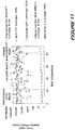
FIGURE 11 shows a plot depicting trace lengths for illustrative run of Symbolic QED according to an aspect of the present disclosure. -
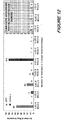
FIGURE 12 shows a plot depicting change detector reduced design results for 92 bugs activated during the FFT and MMULT benchmark tests according to an aspect of the present disclosure; -
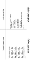
FIGURES 13(A) and 13(B) shows an original test (FIGURE 13(A) ) and a transformed test (FIGURE 13(B) ) of an illustrative EDDI-V example according to the present disclosure with inst_min = inst_max = 3; and -
FIGURES 14(A) and 14(B) shows transformed code (FIGURE 14(A) ) and PLC Operation (FIGURE 14(B) ) for a PLC transformation example with inst_min = inst_max = 4 according to an aspect of the present disclosure; and -
FIGURE 15 shows an illustrative computer system on which methods and structures according to the present disclosure may operate and execute. - The following merely illustrates the principles of the disclosure. It will thus be appreciated that those skilled in the art will be able to devise various arrangements which, although not explicitly described or shown herein, embody the principles of the disclosure and are included within its scope. More particularly, while numerous specific details are set forth, it is understood that embodiments of the disclosure may be practiced without these specific details and in other instances, well-known circuits, structures and techniques have not been shown in order not to obscure the understanding of this disclosure.
- Furthermore, all examples and conditional language recited herein are principally intended expressly to be only for pedagogical purposes to aid the reader in understanding the principles of the disclosure and the concepts contributed by the inventor(s) to furthering the art, and are to be construed as being without limitation to such specifically recited examples and conditions.
- Moreover, all statements herein reciting principles, aspects, and embodiments of the disclosure, as well as specific examples thereof, are intended to encompass both structural and functional equivalents thereof. Additionally, it is intended that such equivalents include both currently-known equivalents as well as equivalents developed in the future, i.e., any elements developed that perform the same function, regardless of structure.
- Thus, for example, it will be appreciated by those skilled in the art that the diagrams herein represent conceptual views of illustrative structures embodying the principles of the disclosure.
- In addition, it will be appreciated by those skilled in art that any flow charts, flow diagrams, state transition diagrams, pseudocode, and the like represent various processes which may be substantially represented in computer readable medium and so executed by a computer or processor, whether or not such computer or processor is explicitly shown.
- In the claims hereof any element expressed as a means for performing a specified function is intended to encompass any way of performing that function including, for example, a) a combination of circuit elements which performs that function or b) software in any form, including, therefore, firmware, microcode or the like, combined with appropriate circuitry for executing that software to perform the function. The invention as defined by such claims resides in the fact that the functionalities provided by the various recited means are combined and brought together in the manner which the claims call for. Applicant thus regards any means which can provide those functionalities as equivalent as those shown herein. Finally, and unless otherwise explicitly specified herein, the drawings are not drawn to scale.
- Thus, for example, it will be appreciated by those skilled in the art that the diagrams herein represent conceptual views of illustrative structures embodying the principles of the disclosure.
- The following Glossary includes definitions provided to assist in further understanding the disclosure.
- Quick Error Detection (QED) - a technique involving the transformation of existing post-silicon validation test(s) into new validation tests that reduce error detection latency. QED transformations allow flexible tradeoffs between error detection latency, coverage, and complexity and may be implemented in software with little or no hardware changes.
- Bug - an error, flaw, failure, or fault in a computer program or system that causes or otherwise contributes to it producing an incorrect or unexpected result or to behave in unintended ways.
- Electrical Bugs - are a type of bug that only manifests itself under specific operating conditions (voltage, frequency, temperature, etc.) and may be caused by design marginalities, synchronization problems, noise, etc.
- Logic bugs - are a type of bug that is caused by one or more design error(s). Logic bugs include incorrect hardware implementations or incorrect interactions between the hardware implementation and low-level system software (e.g., firmware).
- System on a Chip (SoC) - an integrated circuit (IC) that integrates all components of a system into/onto a single chip or integrated package of chips. It may contain digital, analog, mixed-signal, and radio frequency functions. SoC may also refer to technology(ies) that package or otherwise integrate all parts for a system on a single integrated circuit.
- Uncore - are components in a SoC that are neither processor cores nor ∼processors (e.g., graphical processing tmits). Examples of uncore components include cache controllers, memory controllers, and interconnection network.
- The following merely illustrates the principles of the disclosure. It will thus be appreciated that those skilled in the art will be able to devise various arrangements which, although not explicitly described or shown herein, embody the principles of the disclosure and are included within its scope. More particularly, while numerous specific details are set forth, it is understood that embodiments of the disclosure may be practiced without these specific details and in other instances, well-known circuits, structures and techniques have not been shown in order not to obscure the understanding of this disclosure.
- By way of some additional background, we begin by noting that post-silicon validation and debug of integrated circuits has become a critically important step with respect to their design, test, manufacture and support. Generally, post-silicon validation and debug is the last step in the development of a semiconductor IC and occurs between pre-silicon verification and high volume manufacturing.
- Notably, post-silicon verification, validation and debug is contrasted with pre-silicon verification or debug processes, wherein during pre-silicon process(es), devices are generally tested in a virtual environment with sophisticated simulation, emulation and cformal verification tools.
- Unfortunately, pre-silicon verification processes alone are inadequate for verifying correct operation of contemporary ICs and in particular SoCs. As will be appreciated by those skilled in the art, such traditional, prior art pre-silicon techniques are generally too slow and do not adequately address electrical bugs. Consequently, there is growing reliance by those skilled in the art on system-level validation (i.e., emulation) and post-silicon validation (PSV) techniques.
- In sharp contrast to pre-silicon validation processes, during post-silicon validation and debug, actual fabricated ICs are tested in actual system operating environments (i.e., speed, real boards etc. using logic analyzer(s) and other assertion based tools) to detect and fix design or other flaws (generally referred to as bugs). Correct post-silicon validation and debug therefore, is crucial because - as noted above - pre-silicon verification alone is oftentimes inadequate to detect all possible bugs.
- It is noted further that costs of post-silicon validation and debug are rising. Massive integration of a wide variety of components into extremely complex SoCs - which may include multiple processor cores, accelerators for graphics or cryptography as well as uncore components (also referred to as nest or northbridge components) - significantly exacerbates post-silicon validation and debug challenges.
- Generally, post-silicon validation and debug of an IC involves three activities namely:
- 1) Detecting a bug by applying appropriate stimuli (i.e., test programs);
- 2) Localizing the bug to a small region inside the IC; and
- 3) Fixing the bug through software patches, circuit editing, or silicon "re-spin".
- At this point it is noted that effort(s) to localize the bug from an observed failure (post-silicon bug localization) oftentimes dominates the cost(s) of post-silicon validation and debug. Such post-silicon bug localization involves identifying a sequence of inputs (e.g., instructions) that activate and detect the bug (also referred to as a bug trace), and any physical hardware (design block) where the bug is (possibly) located.
- As will be readily appreciated by those skilled in the art, post-silicon bug localization is particularly difficult because many existing post-silicon techniques rely on: 1) system, level simulation to obtain expected or "golden" system response; and/or 2) failure reproduction - which involves returning the system to an error-free state and rerunning the system with the exact input stimuli (e.g., validation test instructions; validation test inputs; voltage, temperature, and frequency operation conditions; and interrupts) - to reproduce the failure.
- Accordingly, methods and structures according to the present disclosure will be appreciated by those skilled in the art as a systematic and automated technique that localizes logic bugs in ICs as well as sophisticated SoCs. As will be further appreciated, without such effective methods and structures for verifying the correct operation of such ICs and SoCs - future systems constructed therefrom will remain vulnerable to logic and electrical bugs that could possibly compromise correct circuit and/or system operation.
- We call methods and structures according to the present disclosure Symbolic Quick Error Detection or Symbolic QED. Illustrative characteristics of Symbolic QED include: 1) It is applicable to any System-on-Chip (SoC) design as long as it contains at least one programmable processor (a generally valid assumption for existing SoCs); 2) It is broadly applicable for logic bugs inside processor cores, accelerators, and uncore components; 3) It does not require failure reproduction; 4) It does not require human intervention during bug localization; 5) It does not require trace buffers; 6) It does not require assertions; and 7) It uses hardware structures called "change detectors" which introduce only a small area overhead (1.86% on OpenSPARC).
- We demonstrate the effectiveness and practicality of Symbolic QED by showing that: 1) Symbolic QED correctly and automatically localizes difficult logic bugs in a few hours (less than 7 on OpenSPARC) that would take days or weeks to localize using traditional approaches; 2) For each detected bug, Symbolic QED provides a set of candidate components representing the possible locations of the bug in the design; 3) For each detected bug, Symbolic QED automatically generates a minimal bug trace using formal analysis; and 4) Symbolic QED generates bug traces that are up to 6 orders of magnitude shorter than those produced by traditional post-silicon techniques and 5 orders of magnitude shorter than QED.
- As we shall describe and will be appreciated by those skilled in the art, Symbolic QED employs the following methodologies which advantageously work together in a coordinated fashion namely, 1) A systematic (and automated) approach to inserting "change detectors" during design phase(s); 2) Quick Error Detection (QED) tests that detect bugs exhibiting short error detection latencies and high coverage; and 3) Formal techniques that enable bug localization and generation of minimal bug traces upon bug detection.
- An overview of Symbolic QED according to the present disclosure may be observed with reference to
FIGURE 1 . As may be observed, Symbolic QED involves two distinct phases namely, a design phase and a post-silicon validation phase. As depicted in that figure, the design phase systematically and automatically inserts change detectors inside a design. The post-silicon validation phase involves running QED tests wherein change detectors record debug information and if errors are detected then localizing bug(s) and producing bug trace reports by formal analysis. - We now present and describe a bug scenario abstracted from an actual - and difficult to detect - bug found during post-silicon validation of a commercial multicore SoC. That scenario is described as: Two stores in 2 cycles to adjacent cache lines in a cache delay the next cache coherence message received by that cache by 5 clock cycles.
- The bug is only activated when two store operations occur within 2 clock cycles of each other to adjacent cache lines. The next cache coherence message (e.g., invalidation) is delayed because of a delay in the receive buffer of the cache (these details were not known before the bug was found and localized).
- During post-silicon validation, a test running on the SoC created a deadlock. As shown in
FIGURE 2 , the deadlock occurs because one of the processor cores (core 4) performs a store to memory location [A] followed by a store to memory location [B] within 2 clock cycles ([A] and [B] are cached on adjacent cache lines). As a result, the example bug scenario is activated incache 4. - After the bug is activated,
processor core 1 performs a store to memory location [C]. Since memory location [C] is cached in multiple caches (cache 1 and cache 4), the store operation to memory location [C] has to invalidate other cached copies of memory location [C] (including the cached copy in cache 4). However, due to the bug, an invalidation message received bycache 4 is delayed by 5 clock cycles. - Before any invalidation occurs,
processor core 4 loads from memory location [C]. Since the cached copy of memory location [C] incache 4 is still marked as valid, it loads this stale copy (which contains the wrong value at this point). Then, millions of clock cycles later,processor core 4 uses the wrong value of memory location [C] in code that performs locking, resulting in deadlock. - When deadlocks such as this are detected (e.g., by using a timeout), the bug must be localized by identifying the bug trace and the component where the bug is located. Since it is not known a priori when the bug was activated or when the system entered deadlock, it can be very difficult to obtain the bug trace.
- Additionally, the bug trace can be extremely long due to the long error detection latency, containing many extraneous instructions unnecessary for activating or detecting the bug. As mentioned above, such bugs can be extremely challenging to localize using traditional approaches like failure reproduction, trace buffers, simulation, or naïve formal methods.
- Advantageously - and as we shall describe - Symbolic QED correctly localizes this bug to
cache 4 and produces a bug trace that is only 3 instructions long. Of further advantage, Symbolic QED produces this trace in only 2.5 hours - automatically - without requiring failure reproduction or trace buffers. - In sharp contrast, traditional post-silicon bug localization approaches would likely require manual effort or trace buffers (or both) and could take days or weeks. Of further advantage, Symbolic QED also provides opportunities for bug detection and localization during emulation-based verification such that even this drastically shortened bug detection and localization may be circumvented entirely by methods according to the present disclosure namely, Symbolic QED.
- Quick Error Detection (QED) - Generic QED is known to quickly detect bugs inside processor cores as well as uncore components. The software-only QED technique automatically transforms existing post-silicon validation tests (original tests) into new QED tests using various QED transformations e.g., Error detection using Duplicated Instructions for Validation (EDDI-V) and Proactive Load and Check (PLC).
- EDDI-V - EDDI-V targets processor core bugs by frequently checking results of original instructions against results of duplicated instructions created by EDDI-V. First, registers and memory space are divided into two halves, one for original instructions and one for duplicated instructions. Next, corresponding registers and memory locations for the original and the duplicated instructions are initialized to the same values. Then, for every load, store, arithmetic, logical, shift, or move instruction in the original test, EDDI-V creates a corresponding duplicate instruction that performs the same operation - but only for registers and memory reserved for duplicate instructions.
- The duplicated instructions execute in the same order as original instructions. The EDDI-V transformation also inserts periodic check instructions (called Normal checks) that compare the results of the original instructions against those of the duplicated instructions.
- Accordingly, for every duplicated load instruction, an additional Load check instruction is inserted immediately after (before the loaded values are used by any other instructions) to check that the value loaded by the original instruction matches the value loaded by the corresponding duplicated instruction. Similarly, for store instructions, a Store check instruction is inserted immediately before the original store instruction to check that the value about to be stored matches the value about to be stored by the duplicated instruction. Each check instruction is of the form:

- PLC - PLC targets bugs inside uncore components by frequently and proactively performing loads from memory (through uncore components) and checking the values loaded. PLC first transforms an original test into an EDDI-V-transformed QED test. Next, PLC inserts Proactive Load and Check (PLC) operations throughout the transformed test. PLC operations run on all cores and all threads.
- Each PLC operation loads from a selected set of variables and performs checks to check the loaded values. Since the PLC test includes EDDI-V, each PLC operation loads a variable A and its duplicated version A' and performs a PLC check as follows: LOCK(A); LOCK(A'); Ra = LD(A) Ra' = LD(A') UNLOCK(A'); UNLOCK(A); CMP Ra, Ra' // compare & detect error Any mismatch indicates an error. Each PLC operation iterates through all the variables selected for PLC check as follows:
                             LOCK(A);
                            LOCK(A');
                            Ra = LD(A)
                            Ra' = LD(A')
                            UNLOCK(A');
                             UNLOCK (A);
                             CMP Ra, Ra' //compare & detect error
 Any mismatch indicates an error. Each PLC operation iterates through all of the
 variables selected for PLC.


- 1. Inputs must be valid instructions (specifications of valid instructions can be directly obtained from Instruction Set Architecture (ISA) of processor cores;
- 2. Registers and memory space(es) are divided into two halves, one for "original" instructions and one for "duplicated" instructions. For every instruction (excluding control-flow changing instructions) that operates on the registers and memory space allocated for the original instructions, there exists a corresponding duplicated instruction that performs the same operation but operates on the registers and memory space allocated for the duplicated instructions.
- 3. The sequence of original instructions and the sequence of duplicated instructions must execute in the same order.
- 4. A comparison (for example, a property checked by the BMC tool) between an original register R and its corresponding register R' occurs only if the original and duplicate instructions are in sync, i.e. for each original instruction that has been executed, its corresponding duplicate instruction has also been executed.

where n is the number of registers defined by the ISA. Here, (for a ∈ {0.. n/2 - 1}), Ra corresponds to a register allocated for original instructions and Ra' corresponds to a register allocated for duplicated instructions. We allow the instructions chosen by BMC to include load and store instructions, enabling our approach to activate and detect bugs in uncore components as well as those in processor cores.

Claims (6)
- A computer implemented method for the post-silicon validation and debug of a digital hardware system, wherein:the digital hardware system is a System on a Chip (SOC) having at least one programmable processor; andthe post-silicon validation method executed by the computer is a Symbolic Quick Error Detection (Symbolic QED) method employing bounded model checking (BMC) that operates byinserting, automatically and systematically a number of change detectors into the digital hardware system during a design phase of that hardware system;running, by a QED module integrated with a fetch unit, a number of quick error detection (QED) tests using QED-compatible traces on that hardware system having the inserted change detectors wherein the change detectors record debug information during the running, the QED-compatible traces comprising a sequence of inputs that are valid instructions obtained from an instruction set architecture of the programmable processor, wherein register and memory spaces are divided into two halves, one for original instructions and one for duplicated instructions, the sequence of original instructions and duplicated instructions execute in the same order, and a comparison between an original register R and its corresponding register R' occurs only if the original and duplicate instructions are in sync;determining, by the computer performing the BMC, whether an error (bug) was detected by the QED tests, wherein an initial state of the BMC is a QED-consistent state wherein a value of each register and memory location allocated for original instructions matches the corresponding register or memory location for duplication instructions such that no false counter-examples are generated; andif a bug was detected by the QED tests then localizing the detected bug and generating a minimal bug trace having less than 10 instructions.
- The computer implemented method of claim 1 further comprising:inserting change detectors to record changes in logic values of signals during validation, said change detectors inserted at boundaries of all components that may be removed in a further analysis;stopping the system when QED test(s) detects an error;saving any change detector value(s); andusing the saved change detector value(s), generating a reduced design for further analysis;wherein the reduced design excludes any components from BMC analysis if, during a change window, change detector(s) associated with those components did not record any changes in the logic values of the components input or output signals.
- The computer implemented method of claim 1 wherein the QED employs a number of QED transformations selected from the group consisting of Error Detection using Duplicated Instructions for Validation (EDDI-V) and Proactive Load and Check (PLC) transformations.
- The computer implemented method according to claim 1 comprising ensuring that only QED-compatible bug traces are considered by BMC by adding a new QED module to a fetch stage of each processor core during BMC.
- The computer implemented method of claim 1 wherein the change detectors include a k-bit ripple counter that is initialized to all 1's and is reset to all 0's whenever a change in signal value is detected.
- The computer implemented method of claim 5 wherein the change detectors are inserted at boundaries of all components that may potentially be removed during a further analysis.
Applications Claiming Priority (2)
| Application Number | Priority Date | Filing Date | Title |
|---|---|---|---|
| US201562172091P | 2015-06-06 | 2015-06-06 | |
| PCT/US2016/035987 WO2016200723A1 (en) | 2015-06-06 | 2016-06-06 | Post-silicon validation and debug using symbolic quick error detection |
Publications (3)
| Publication Number | Publication Date |
|---|---|
| EP3304312A1 EP3304312A1 (en) | 2018-04-11 |
| EP3304312A4 EP3304312A4 (en) | 2018-06-13 |
| EP3304312B1 true EP3304312B1 (en) | 2020-02-12 |
Family
ID=57504703
Family Applications (1)
| Application Number | Title | Priority Date | Filing Date |
|---|---|---|---|
| EP16808080.2A Active EP3304312B1 (en) | 2015-06-06 | 2016-06-06 | Post-silicon validation and debug using symbolic quick error detection |
Country Status (4)
| Country | Link |
|---|---|
| US (1) | US10528448B2 (en) |
| EP (1) | EP3304312B1 (en) |
| CN (1) | CN107710166B (en) |
| WO (1) | WO2016200723A1 (en) |
Families Citing this family (10)
| Publication number | Priority date | Publication date | Assignee | Title |
|---|---|---|---|---|
| EP3304111B1 (en) * | 2015-06-06 | 2020-03-11 | The Board of Trustees of the Leland Stanford Junior University | System-level validation of systems-on-a-chip (soc) |
| US10295596B1 (en) * | 2017-08-09 | 2019-05-21 | Cadence Design Systems, Inc. | Method and system for generating validation tests |
| US10783304B1 (en) * | 2018-09-28 | 2020-09-22 | Cadence Design Systems, Inc. | System, method, and computer program product for displaying debugging during a formal verification |
| EP3715975B1 (en) * | 2019-03-28 | 2023-03-01 | Mitsubishi Electric R&D Centre Europe B.V. | Method and apparatus for analysing a ladder program |
| CN110032482A (en) * | 2019-04-11 | 2019-07-19 | 盛科网络(苏州)有限公司 | Sheet sand covered device and method |
| US11204859B2 (en) | 2019-07-09 | 2021-12-21 | International Business Machines Corporation | Partial-results post-silicon hardware exerciser |
| US11119890B2 (en) * | 2019-08-28 | 2021-09-14 | International Business Machines Corporation | Instruction level tracing for analyzing processor failure |
| US11030370B2 (en) | 2019-09-30 | 2021-06-08 | International Business Machines Corporation | Modular event-based performance monitoring in integrated circuit development |
| US11501046B2 (en) * | 2020-03-24 | 2022-11-15 | International Business Machines Corporation | Pre-silicon chip model of extracted workload inner loop instruction traces |
| US20230401130A1 (en) * | 2022-06-14 | 2023-12-14 | Intel Corporation | Fpga based platform for post-silicon validation of chiplets |
Family Cites Families (13)
| Publication number | Priority date | Publication date | Assignee | Title |
|---|---|---|---|---|
| DE4223955A1 (en) * | 1992-07-21 | 1994-01-27 | Bosch Gmbh Robert | Method and device for determining the amount of fuel supplied to an internal combustion engine |
| EP2256634A1 (en) * | 2009-05-27 | 2010-12-01 | Robert Bosch Gmbh | A data processing device and a method for error detection and error correction |
| US8327198B2 (en) * | 2009-08-14 | 2012-12-04 | Intel Corporation | On-die logic analyzer for semiconductor die |
| US20110087861A1 (en) * | 2009-10-12 | 2011-04-14 | The Regents Of The University Of Michigan | System for High-Efficiency Post-Silicon Verification of a Processor |
| CN101714118B (en) * | 2009-11-20 | 2011-06-22 | 北京邮电大学 | A binary code buffer overflow vulnerability detector and its detection method |
| WO2012031362A1 (en) | 2010-09-07 | 2012-03-15 | Corporation De L ' Ecole Polytechnique De Montreal | Methods, apparatus and system to support large-scale micro- systems including embedded and distributed power supply, thermal regulation, multi-distributed-sensors and electrical signal propagation |
| DE112010006087T5 (en) | 2010-12-23 | 2014-06-26 | Intel Corporation | Architecture for testing, validation and debugging |
| US8799715B2 (en) * | 2012-06-26 | 2014-08-05 | Apple Inc. | System on a chip (SOC) debug controllability |
| CN102818337B (en) * | 2012-07-13 | 2014-10-29 | 华中科技大学 | Device for monitoring ground source heat pump system based on internet of things |
| US9411007B2 (en) * | 2012-10-29 | 2016-08-09 | The Regents Of The University Of Michigan | System and method for statistical post-silicon validation |
| CN103900071A (en) * | 2014-03-10 | 2014-07-02 | 杭州齐曼节能环保技术有限公司 | Coal-fired boiler interactive online monitoring method |
| CN103905464B (en) * | 2014-04-21 | 2017-03-01 | 西安电子科技大学 | Network security policy checking system based on formalization method and method |
| US9928150B2 (en) * | 2014-06-30 | 2018-03-27 | The Board Of Trustees Of The Leland Stanford Junior University | System and method for testing a logic-based processing device |
-
2016
- 2016-06-06 CN CN201680034767.3A patent/CN107710166B/en not_active Expired - Fee Related
- 2016-06-06 WO PCT/US2016/035987 patent/WO2016200723A1/en not_active Ceased
- 2016-06-06 US US15/577,065 patent/US10528448B2/en active Active
- 2016-06-06 EP EP16808080.2A patent/EP3304312B1/en active Active
Non-Patent Citations (1)
| Title |
|---|
| None * |
Also Published As
| Publication number | Publication date |
|---|---|
| US10528448B2 (en) | 2020-01-07 |
| EP3304312A4 (en) | 2018-06-13 |
| WO2016200723A1 (en) | 2016-12-15 |
| CN107710166B (en) | 2021-06-18 |
| US20180157574A1 (en) | 2018-06-07 |
| EP3304312A1 (en) | 2018-04-11 |
| CN107710166A (en) | 2018-02-16 |
Similar Documents
| Publication | Publication Date | Title |
|---|---|---|
| US10528448B2 (en) | Post-silicon validation and debug using symbolic quick error detection | |
| Hangal et al. | TSOtool: A program for verifying memory systems using the memory consistency model | |
| Lin et al. | A structured approach to post-silicon validation and debug using symbolic quick error detection | |
| US8121825B2 (en) | Method and apparatus for executing a hardware simulation and verification solution | |
| Lin et al. | Effective post-silicon validation of system-on-chips using quick error detection | |
| US9928150B2 (en) | System and method for testing a logic-based processing device | |
| Singh et al. | Logic bug detection and localization using symbolic quick error detection | |
| Lin et al. | Quick detection of difficult bugs for effective post-silicon validation | |
| CN107850641B (en) | System-level verification of system-on-chip (SoC) | |
| US12340155B2 (en) | Detecting instability in combinational loops in electronic circuit designs | |
| Lin et al. | Quick error detection tests with fast runtimes for effective post-silicon validation and debug | |
| Singh et al. | Symbolic qed pre-silicon verification for automotive microcontroller cores: Industrial case study | |
| Dehbashi et al. | Debug automation for synchronization bugs at RTL | |
| Dadashi et al. | Hardware-software integrated diagnosis for intermittent hardware faults | |
| Arbel et al. | Automated detection and verification of parity-protected memory elements | |
| Bartsch et al. | A HW/SW cross-layer approach for determining application-redundant hardware faults in embedded systems | |
| Bartsch et al. | A HW-dependent software model for cross-layer fault analysis in embedded systems | |
| US12585561B2 (en) | Technique for generating tests for a processing device | |
| US20250035697A1 (en) | Bias cause reduction for localizing constraints | |
| Tabacaru et al. | Gate-level-accurate fault-effect analysis at virtual-prototype speed | |
| Chibani et al. | Application-aware soft error sensitivity evaluation without fault injections—application to Leon3 | |
| US11062069B1 (en) | Bounded deadlock check | |
| Iyer et al. | RTL bug localization through LTL specification mining (WIP) | |
| Fernandes | Automatic Testing of Persistent Memory Applications | |
| Arbel et al. | Gating aware error injection |
Legal Events
| Date | Code | Title | Description |
|---|---|---|---|
| STAA | Information on the status of an ep patent application or granted ep patent |
Free format text: STATUS: THE INTERNATIONAL PUBLICATION HAS BEEN MADE |
|
| PUAI | Public reference made under article 153(3) epc to a published international application that has entered the european phase |
Free format text: ORIGINAL CODE: 0009012 |
|
| STAA | Information on the status of an ep patent application or granted ep patent |
Free format text: STATUS: REQUEST FOR EXAMINATION WAS MADE |
|
| 17P | Request for examination filed |
Effective date: 20171113 |
|
| AK | Designated contracting states |
Kind code of ref document: A1 Designated state(s): AL AT BE BG CH CY CZ DE DK EE ES FI FR GB GR HR HU IE IS IT LI LT LU LV MC MK MT NL NO PL PT RO RS SE SI SK SM TR |
|
| AX | Request for extension of the european patent |
Extension state: BA ME |
|
| A4 | Supplementary search report drawn up and despatched |
Effective date: 20180516 |
|
| RIC1 | Information provided on ipc code assigned before grant |
Ipc: G06F 11/34 20060101ALI20180509BHEP Ipc: G06F 11/30 20060101ALI20180509BHEP Ipc: G06F 11/273 20060101AFI20180509BHEP Ipc: G06F 11/22 20060101ALI20180509BHEP Ipc: H01L 21/66 20060101ALI20180509BHEP |
|
| DAV | Request for validation of the european patent (deleted) | ||
| DAX | Request for extension of the european patent (deleted) | ||
| GRAP | Despatch of communication of intention to grant a patent |
Free format text: ORIGINAL CODE: EPIDOSNIGR1 |
|
| STAA | Information on the status of an ep patent application or granted ep patent |
Free format text: STATUS: GRANT OF PATENT IS INTENDED |
|
| RAP1 | Party data changed (applicant data changed or rights of an application transferred) |
Owner name: NEW YORK UNIVERSITY Owner name: THE BOARD OF TRUSTEES OF THE LELAND STANFORD JUNIO |
|
| INTG | Intention to grant announced |
Effective date: 20190904 |
|
| GRAS | Grant fee paid |
Free format text: ORIGINAL CODE: EPIDOSNIGR3 |
|
| GRAA | (expected) grant |
Free format text: ORIGINAL CODE: 0009210 |
|
| STAA | Information on the status of an ep patent application or granted ep patent |
Free format text: STATUS: THE PATENT HAS BEEN GRANTED |
|
| AK | Designated contracting states |
Kind code of ref document: B1 Designated state(s): AL AT BE BG CH CY CZ DE DK EE ES FI FR GB GR HR HU IE IS IT LI LT LU LV MC MK MT NL NO PL PT RO RS SE SI SK SM TR |
|
| REG | Reference to a national code |
Ref country code: GB Ref legal event code: FG4D |
|
| REG | Reference to a national code |
Ref country code: CH Ref legal event code: EP |
|
| REG | Reference to a national code |
Ref country code: AT Ref legal event code: REF Ref document number: 1233043 Country of ref document: AT Kind code of ref document: T Effective date: 20200215 |
|
| REG | Reference to a national code |
Ref country code: DE Ref legal event code: R096 Ref document number: 602016029717 Country of ref document: DE |
|
| REG | Reference to a national code |
Ref country code: IE Ref legal event code: FG4D |
|
| REG | Reference to a national code |
Ref country code: NL Ref legal event code: FP |
|
| PG25 | Lapsed in a contracting state [announced via postgrant information from national office to epo] |
Ref country code: RS Free format text: LAPSE BECAUSE OF FAILURE TO SUBMIT A TRANSLATION OF THE DESCRIPTION OR TO PAY THE FEE WITHIN THE PRESCRIBED TIME-LIMIT Effective date: 20200212 Ref country code: FI Free format text: LAPSE BECAUSE OF FAILURE TO SUBMIT A TRANSLATION OF THE DESCRIPTION OR TO PAY THE FEE WITHIN THE PRESCRIBED TIME-LIMIT Effective date: 20200212 Ref country code: NO Free format text: LAPSE BECAUSE OF FAILURE TO SUBMIT A TRANSLATION OF THE DESCRIPTION OR TO PAY THE FEE WITHIN THE PRESCRIBED TIME-LIMIT Effective date: 20200512 |
|
| REG | Reference to a national code |
Ref country code: LT Ref legal event code: MG4D |
|
| PG25 | Lapsed in a contracting state [announced via postgrant information from national office to epo] |
Ref country code: SE Free format text: LAPSE BECAUSE OF FAILURE TO SUBMIT A TRANSLATION OF THE DESCRIPTION OR TO PAY THE FEE WITHIN THE PRESCRIBED TIME-LIMIT Effective date: 20200212 Ref country code: LV Free format text: LAPSE BECAUSE OF FAILURE TO SUBMIT A TRANSLATION OF THE DESCRIPTION OR TO PAY THE FEE WITHIN THE PRESCRIBED TIME-LIMIT Effective date: 20200212 Ref country code: IS Free format text: LAPSE BECAUSE OF FAILURE TO SUBMIT A TRANSLATION OF THE DESCRIPTION OR TO PAY THE FEE WITHIN THE PRESCRIBED TIME-LIMIT Effective date: 20200612 Ref country code: BG Free format text: LAPSE BECAUSE OF FAILURE TO SUBMIT A TRANSLATION OF THE DESCRIPTION OR TO PAY THE FEE WITHIN THE PRESCRIBED TIME-LIMIT Effective date: 20200512 Ref country code: HR Free format text: LAPSE BECAUSE OF FAILURE TO SUBMIT A TRANSLATION OF THE DESCRIPTION OR TO PAY THE FEE WITHIN THE PRESCRIBED TIME-LIMIT Effective date: 20200212 Ref country code: GR Free format text: LAPSE BECAUSE OF FAILURE TO SUBMIT A TRANSLATION OF THE DESCRIPTION OR TO PAY THE FEE WITHIN THE PRESCRIBED TIME-LIMIT Effective date: 20200513 |
|
| PG25 | Lapsed in a contracting state [announced via postgrant information from national office to epo] |
Ref country code: EE Free format text: LAPSE BECAUSE OF FAILURE TO SUBMIT A TRANSLATION OF THE DESCRIPTION OR TO PAY THE FEE WITHIN THE PRESCRIBED TIME-LIMIT Effective date: 20200212 Ref country code: LT Free format text: LAPSE BECAUSE OF FAILURE TO SUBMIT A TRANSLATION OF THE DESCRIPTION OR TO PAY THE FEE WITHIN THE PRESCRIBED TIME-LIMIT Effective date: 20200212 Ref country code: SM Free format text: LAPSE BECAUSE OF FAILURE TO SUBMIT A TRANSLATION OF THE DESCRIPTION OR TO PAY THE FEE WITHIN THE PRESCRIBED TIME-LIMIT Effective date: 20200212 Ref country code: DK Free format text: LAPSE BECAUSE OF FAILURE TO SUBMIT A TRANSLATION OF THE DESCRIPTION OR TO PAY THE FEE WITHIN THE PRESCRIBED TIME-LIMIT Effective date: 20200212 Ref country code: PT Free format text: LAPSE BECAUSE OF FAILURE TO SUBMIT A TRANSLATION OF THE DESCRIPTION OR TO PAY THE FEE WITHIN THE PRESCRIBED TIME-LIMIT Effective date: 20200705 Ref country code: SK Free format text: LAPSE BECAUSE OF FAILURE TO SUBMIT A TRANSLATION OF THE DESCRIPTION OR TO PAY THE FEE WITHIN THE PRESCRIBED TIME-LIMIT Effective date: 20200212 Ref country code: CZ Free format text: LAPSE BECAUSE OF FAILURE TO SUBMIT A TRANSLATION OF THE DESCRIPTION OR TO PAY THE FEE WITHIN THE PRESCRIBED TIME-LIMIT Effective date: 20200212 Ref country code: ES Free format text: LAPSE BECAUSE OF FAILURE TO SUBMIT A TRANSLATION OF THE DESCRIPTION OR TO PAY THE FEE WITHIN THE PRESCRIBED TIME-LIMIT Effective date: 20200212 Ref country code: RO Free format text: LAPSE BECAUSE OF FAILURE TO SUBMIT A TRANSLATION OF THE DESCRIPTION OR TO PAY THE FEE WITHIN THE PRESCRIBED TIME-LIMIT Effective date: 20200212 |
|
| REG | Reference to a national code |
Ref country code: DE Ref legal event code: R097 Ref document number: 602016029717 Country of ref document: DE |
|
| REG | Reference to a national code |
Ref country code: AT Ref legal event code: MK05 Ref document number: 1233043 Country of ref document: AT Kind code of ref document: T Effective date: 20200212 |
|
| PLBE | No opposition filed within time limit |
Free format text: ORIGINAL CODE: 0009261 |
|
| STAA | Information on the status of an ep patent application or granted ep patent |
Free format text: STATUS: NO OPPOSITION FILED WITHIN TIME LIMIT |
|
| 26N | No opposition filed |
Effective date: 20201113 |
|
| PG25 | Lapsed in a contracting state [announced via postgrant information from national office to epo] |
Ref country code: IT Free format text: LAPSE BECAUSE OF FAILURE TO SUBMIT A TRANSLATION OF THE DESCRIPTION OR TO PAY THE FEE WITHIN THE PRESCRIBED TIME-LIMIT Effective date: 20200212 Ref country code: MC Free format text: LAPSE BECAUSE OF FAILURE TO SUBMIT A TRANSLATION OF THE DESCRIPTION OR TO PAY THE FEE WITHIN THE PRESCRIBED TIME-LIMIT Effective date: 20200212 Ref country code: AT Free format text: LAPSE BECAUSE OF FAILURE TO SUBMIT A TRANSLATION OF THE DESCRIPTION OR TO PAY THE FEE WITHIN THE PRESCRIBED TIME-LIMIT Effective date: 20200212 |
|
| REG | Reference to a national code |
Ref country code: CH Ref legal event code: PL |
|
| PG25 | Lapsed in a contracting state [announced via postgrant information from national office to epo] |
Ref country code: SI Free format text: LAPSE BECAUSE OF FAILURE TO SUBMIT A TRANSLATION OF THE DESCRIPTION OR TO PAY THE FEE WITHIN THE PRESCRIBED TIME-LIMIT Effective date: 20200212 Ref country code: PL Free format text: LAPSE BECAUSE OF FAILURE TO SUBMIT A TRANSLATION OF THE DESCRIPTION OR TO PAY THE FEE WITHIN THE PRESCRIBED TIME-LIMIT Effective date: 20200212 |
|
| PG25 | Lapsed in a contracting state [announced via postgrant information from national office to epo] |
Ref country code: LU Free format text: LAPSE BECAUSE OF NON-PAYMENT OF DUE FEES Effective date: 20200606 |
|
| REG | Reference to a national code |
Ref country code: BE Ref legal event code: MM Effective date: 20200630 |
|
| PG25 | Lapsed in a contracting state [announced via postgrant information from national office to epo] |
Ref country code: IE Free format text: LAPSE BECAUSE OF NON-PAYMENT OF DUE FEES Effective date: 20200606 Ref country code: CH Free format text: LAPSE BECAUSE OF NON-PAYMENT OF DUE FEES Effective date: 20200630 Ref country code: LI Free format text: LAPSE BECAUSE OF NON-PAYMENT OF DUE FEES Effective date: 20200630 |
|
| PG25 | Lapsed in a contracting state [announced via postgrant information from national office to epo] |
Ref country code: BE Free format text: LAPSE BECAUSE OF NON-PAYMENT OF DUE FEES Effective date: 20200630 |
|
| PG25 | Lapsed in a contracting state [announced via postgrant information from national office to epo] |
Ref country code: TR Free format text: LAPSE BECAUSE OF FAILURE TO SUBMIT A TRANSLATION OF THE DESCRIPTION OR TO PAY THE FEE WITHIN THE PRESCRIBED TIME-LIMIT Effective date: 20200212 Ref country code: MT Free format text: LAPSE BECAUSE OF FAILURE TO SUBMIT A TRANSLATION OF THE DESCRIPTION OR TO PAY THE FEE WITHIN THE PRESCRIBED TIME-LIMIT Effective date: 20200212 Ref country code: CY Free format text: LAPSE BECAUSE OF FAILURE TO SUBMIT A TRANSLATION OF THE DESCRIPTION OR TO PAY THE FEE WITHIN THE PRESCRIBED TIME-LIMIT Effective date: 20200212 |
|
| PG25 | Lapsed in a contracting state [announced via postgrant information from national office to epo] |
Ref country code: MK Free format text: LAPSE BECAUSE OF FAILURE TO SUBMIT A TRANSLATION OF THE DESCRIPTION OR TO PAY THE FEE WITHIN THE PRESCRIBED TIME-LIMIT Effective date: 20200212 Ref country code: AL Free format text: LAPSE BECAUSE OF FAILURE TO SUBMIT A TRANSLATION OF THE DESCRIPTION OR TO PAY THE FEE WITHIN THE PRESCRIBED TIME-LIMIT Effective date: 20200212 |
|
| PGFP | Annual fee paid to national office [announced via postgrant information from national office to epo] |
Ref country code: NL Payment date: 20220606 Year of fee payment: 7 Ref country code: GB Payment date: 20220620 Year of fee payment: 7 |
|
| PGFP | Annual fee paid to national office [announced via postgrant information from national office to epo] |
Ref country code: FR Payment date: 20220628 Year of fee payment: 7 |
|
| PGFP | Annual fee paid to national office [announced via postgrant information from national office to epo] |
Ref country code: DE Payment date: 20220804 Year of fee payment: 7 |
|
| REG | Reference to a national code |
Ref country code: DE Ref legal event code: R119 Ref document number: 602016029717 Country of ref document: DE |
|
| REG | Reference to a national code |
Ref country code: NL Ref legal event code: MM Effective date: 20230701 |
|
| GBPC | Gb: european patent ceased through non-payment of renewal fee |
Effective date: 20230606 |
|
| PG25 | Lapsed in a contracting state [announced via postgrant information from national office to epo] |
Ref country code: NL Free format text: LAPSE BECAUSE OF NON-PAYMENT OF DUE FEES Effective date: 20230701 |
|
| PG25 | Lapsed in a contracting state [announced via postgrant information from national office to epo] |
Ref country code: DE Free format text: LAPSE BECAUSE OF NON-PAYMENT OF DUE FEES Effective date: 20240103 Ref country code: GB Free format text: LAPSE BECAUSE OF NON-PAYMENT OF DUE FEES Effective date: 20230606 |
|
| PG25 | Lapsed in a contracting state [announced via postgrant information from national office to epo] |
Ref country code: FR Free format text: LAPSE BECAUSE OF NON-PAYMENT OF DUE FEES Effective date: 20230630 |