EP3302010A1 - Circuit board and method for producing a circuit board - Google Patents
Circuit board and method for producing a circuit board Download PDFInfo
- Publication number
- EP3302010A1 EP3302010A1 EP16191872.7A EP16191872A EP3302010A1 EP 3302010 A1 EP3302010 A1 EP 3302010A1 EP 16191872 A EP16191872 A EP 16191872A EP 3302010 A1 EP3302010 A1 EP 3302010A1
- Authority
- EP
- European Patent Office
- Prior art keywords
- copper
- carrier
- metal foil
- coating
- ceramic surface
- Prior art date
- Legal status (The legal status is an assumption and is not a legal conclusion. Google has not performed a legal analysis and makes no representation as to the accuracy of the status listed.)
- Withdrawn
Links
- 238000004519 manufacturing process Methods 0.000 title abstract description 12
- 239000010949 copper Substances 0.000 claims abstract description 257
- 229910052802 copper Inorganic materials 0.000 claims abstract description 256
- RYGMFSIKBFXOCR-UHFFFAOYSA-N Copper Chemical compound [Cu] RYGMFSIKBFXOCR-UHFFFAOYSA-N 0.000 claims abstract description 254
- 239000000919 ceramic Substances 0.000 claims abstract description 120
- 239000011888 foil Substances 0.000 claims abstract description 120
- 229910052751 metal Inorganic materials 0.000 claims abstract description 115
- 239000002184 metal Substances 0.000 claims abstract description 115
- 238000001465 metallisation Methods 0.000 claims abstract description 78
- 239000011248 coating agent Substances 0.000 claims abstract description 29
- 238000000576 coating method Methods 0.000 claims abstract description 29
- QVGXLLKOCUKJST-UHFFFAOYSA-N atomic oxygen Chemical compound [O] QVGXLLKOCUKJST-UHFFFAOYSA-N 0.000 claims abstract description 9
- 229910052760 oxygen Inorganic materials 0.000 claims abstract description 9
- 239000001301 oxygen Substances 0.000 claims abstract description 9
- 230000005496 eutectics Effects 0.000 claims abstract description 4
- 230000015572 biosynthetic process Effects 0.000 claims abstract description 3
- 238000000034 method Methods 0.000 claims description 71
- 239000000463 material Substances 0.000 claims description 47
- 238000010438 heat treatment Methods 0.000 claims description 40
- 239000007789 gas Substances 0.000 claims description 36
- 238000001816 cooling Methods 0.000 claims description 24
- QPLDLSVMHZLSFG-UHFFFAOYSA-N Copper oxide Chemical compound [Cu]=O QPLDLSVMHZLSFG-UHFFFAOYSA-N 0.000 claims description 15
- 239000005751 Copper oxide Substances 0.000 claims description 11
- 229910000431 copper oxide Inorganic materials 0.000 claims description 11
- 239000012530 fluid Substances 0.000 claims description 9
- 239000011800 void material Substances 0.000 claims description 9
- 238000000151 deposition Methods 0.000 claims description 6
- 238000002844 melting Methods 0.000 claims description 5
- 230000008018 melting Effects 0.000 claims description 5
- JJLJMEJHUUYSSY-UHFFFAOYSA-L copper(II) hydroxide Inorganic materials [OH-].[OH-].[Cu+2] JJLJMEJHUUYSSY-UHFFFAOYSA-L 0.000 claims description 4
- OPQARKPSCNTWTJ-UHFFFAOYSA-L copper(ii) acetate Chemical compound [Cu+2].CC([O-])=O.CC([O-])=O OPQARKPSCNTWTJ-UHFFFAOYSA-L 0.000 claims description 4
- 238000005229 chemical vapour deposition Methods 0.000 claims description 3
- 238000001035 drying Methods 0.000 claims description 3
- 238000005240 physical vapour deposition Methods 0.000 claims description 3
- 238000005507 spraying Methods 0.000 claims description 3
- AEJIMXVJZFYIHN-UHFFFAOYSA-N copper;dihydrate Chemical compound O.O.[Cu] AEJIMXVJZFYIHN-UHFFFAOYSA-N 0.000 claims description 2
- 230000001590 oxidative effect Effects 0.000 claims 1
- 239000000758 substrate Substances 0.000 claims 1
- 239000004065 semiconductor Substances 0.000 description 23
- 239000007788 liquid Substances 0.000 description 17
- 239000000203 mixture Substances 0.000 description 6
- 238000004140 cleaning Methods 0.000 description 5
- 230000005684 electric field Effects 0.000 description 5
- 239000011146 organic particle Substances 0.000 description 5
- 239000007787 solid Substances 0.000 description 5
- BASFCYQUMIYNBI-UHFFFAOYSA-N platinum Chemical compound [Pt] BASFCYQUMIYNBI-UHFFFAOYSA-N 0.000 description 4
- 238000011946 reduction process Methods 0.000 description 4
- 230000002829 reductive effect Effects 0.000 description 4
- PNEYBMLMFCGWSK-UHFFFAOYSA-N Alumina Chemical compound [O-2].[O-2].[O-2].[Al+3].[Al+3] PNEYBMLMFCGWSK-UHFFFAOYSA-N 0.000 description 3
- 238000005137 deposition process Methods 0.000 description 3
- 238000005530 etching Methods 0.000 description 3
- 239000010931 gold Substances 0.000 description 3
- 238000001513 hot isostatic pressing Methods 0.000 description 3
- XKRFYHLGVUSROY-UHFFFAOYSA-N Argon Chemical compound [Ar] XKRFYHLGVUSROY-UHFFFAOYSA-N 0.000 description 2
- FGUUSXIOTUKUDN-IBGZPJMESA-N C1(=CC=CC=C1)N1C2=C(NC([C@H](C1)NC=1OC(=NN=1)C1=CC=CC=C1)=O)C=CC=C2 Chemical compound C1(=CC=CC=C1)N1C2=C(NC([C@H](C1)NC=1OC(=NN=1)C1=CC=CC=C1)=O)C=CC=C2 FGUUSXIOTUKUDN-IBGZPJMESA-N 0.000 description 2
- BQCADISMDOOEFD-UHFFFAOYSA-N Silver Chemical compound [Ag] BQCADISMDOOEFD-UHFFFAOYSA-N 0.000 description 2
- XLOMVQKBTHCTTD-UHFFFAOYSA-N Zinc monoxide Chemical compound [Zn]=O XLOMVQKBTHCTTD-UHFFFAOYSA-N 0.000 description 2
- 239000000969 carrier Substances 0.000 description 2
- 238000007796 conventional method Methods 0.000 description 2
- BERDEBHAJNAUOM-UHFFFAOYSA-N copper(I) oxide Inorganic materials [Cu]O[Cu] BERDEBHAJNAUOM-UHFFFAOYSA-N 0.000 description 2
- KRFJLUBVMFXRPN-UHFFFAOYSA-N cuprous oxide Chemical compound [O-2].[Cu+].[Cu+] KRFJLUBVMFXRPN-UHFFFAOYSA-N 0.000 description 2
- 238000010494 dissociation reaction Methods 0.000 description 2
- 230000005593 dissociations Effects 0.000 description 2
- 230000005669 field effect Effects 0.000 description 2
- 238000010304 firing Methods 0.000 description 2
- 229910052737 gold Inorganic materials 0.000 description 2
- 238000005304 joining Methods 0.000 description 2
- 229910000510 noble metal Inorganic materials 0.000 description 2
- 239000002245 particle Substances 0.000 description 2
- 229910052697 platinum Inorganic materials 0.000 description 2
- 238000005498 polishing Methods 0.000 description 2
- 229910052709 silver Inorganic materials 0.000 description 2
- 238000004544 sputter deposition Methods 0.000 description 2
- AANMVENRNJYEMK-UHFFFAOYSA-N 4-propan-2-ylcyclohex-2-en-1-one Chemical compound CC(C)C1CCC(=O)C=C1 AANMVENRNJYEMK-UHFFFAOYSA-N 0.000 description 1
- 229910017083 AlN Inorganic materials 0.000 description 1
- PIGFYZPCRLYGLF-UHFFFAOYSA-N Aluminum nitride Chemical compound [Al]#N PIGFYZPCRLYGLF-UHFFFAOYSA-N 0.000 description 1
- IJGRMHOSHXDMSA-UHFFFAOYSA-N Atomic nitrogen Chemical compound N#N IJGRMHOSHXDMSA-UHFFFAOYSA-N 0.000 description 1
- PZNSFCLAULLKQX-UHFFFAOYSA-N Boron nitride Chemical compound N#B PZNSFCLAULLKQX-UHFFFAOYSA-N 0.000 description 1
- 229910052581 Si3N4 Inorganic materials 0.000 description 1
- WZECUPJJEIXUKY-UHFFFAOYSA-N [O-2].[O-2].[O-2].[U+6] Chemical compound [O-2].[O-2].[O-2].[U+6] WZECUPJJEIXUKY-UHFFFAOYSA-N 0.000 description 1
- 239000000853 adhesive Substances 0.000 description 1
- 230000001070 adhesive effect Effects 0.000 description 1
- 229910045601 alloy Inorganic materials 0.000 description 1
- 239000000956 alloy Substances 0.000 description 1
- 229910052782 aluminium Inorganic materials 0.000 description 1
- 239000004411 aluminium Substances 0.000 description 1
- XAGFODPZIPBFFR-UHFFFAOYSA-N aluminium Chemical compound [Al] XAGFODPZIPBFFR-UHFFFAOYSA-N 0.000 description 1
- 229910052786 argon Inorganic materials 0.000 description 1
- JRPBQTZRNDNNOP-UHFFFAOYSA-N barium titanate Chemical compound [Ba+2].[Ba+2].[O-][Ti]([O-])([O-])[O-] JRPBQTZRNDNNOP-UHFFFAOYSA-N 0.000 description 1
- 229910002113 barium titanate Inorganic materials 0.000 description 1
- 229910010293 ceramic material Inorganic materials 0.000 description 1
- 229910052729 chemical element Inorganic materials 0.000 description 1
- NFFYXVOHHLQALV-UHFFFAOYSA-N copper(III) oxide Inorganic materials [O-2].[O-2].[O-2].[Cu].[Cu] NFFYXVOHHLQALV-UHFFFAOYSA-N 0.000 description 1
- 239000000428 dust Substances 0.000 description 1
- 230000002349 favourable effect Effects 0.000 description 1
- 238000011010 flushing procedure Methods 0.000 description 1
- PCHJSUWPFVWCPO-UHFFFAOYSA-N gold Chemical compound [Au] PCHJSUWPFVWCPO-UHFFFAOYSA-N 0.000 description 1
- 239000001307 helium Substances 0.000 description 1
- 229910052734 helium Inorganic materials 0.000 description 1
- SWQJXJOGLNCZEY-UHFFFAOYSA-N helium atom Chemical compound [He] SWQJXJOGLNCZEY-UHFFFAOYSA-N 0.000 description 1
- 238000000462 isostatic pressing Methods 0.000 description 1
- 229910052749 magnesium Inorganic materials 0.000 description 1
- 239000011777 magnesium Substances 0.000 description 1
- -1 magnesium aluminate Chemical class 0.000 description 1
- CPLXHLVBOLITMK-UHFFFAOYSA-N magnesium oxide Inorganic materials [Mg]=O CPLXHLVBOLITMK-UHFFFAOYSA-N 0.000 description 1
- 239000000395 magnesium oxide Substances 0.000 description 1
- AXZKOIWUVFPNLO-UHFFFAOYSA-N magnesium;oxygen(2-) Chemical compound [O-2].[Mg+2] AXZKOIWUVFPNLO-UHFFFAOYSA-N 0.000 description 1
- 229910044991 metal oxide Inorganic materials 0.000 description 1
- 150000004706 metal oxides Chemical class 0.000 description 1
- 229910052754 neon Inorganic materials 0.000 description 1
- GKAOGPIIYCISHV-UHFFFAOYSA-N neon atom Chemical compound [Ne] GKAOGPIIYCISHV-UHFFFAOYSA-N 0.000 description 1
- RVTZCBVAJQQJTK-UHFFFAOYSA-N oxygen(2-);zirconium(4+) Chemical compound [O-2].[O-2].[Zr+4] RVTZCBVAJQQJTK-UHFFFAOYSA-N 0.000 description 1
- 239000000843 powder Substances 0.000 description 1
- 238000003825 pressing Methods 0.000 description 1
- HQVNEWCFYHHQES-UHFFFAOYSA-N silicon nitride Chemical compound N12[Si]34N5[Si]62N3[Si]51N64 HQVNEWCFYHHQES-UHFFFAOYSA-N 0.000 description 1
- 239000004332 silver Substances 0.000 description 1
- 239000010944 silver (metal) Substances 0.000 description 1
- 229910000679 solder Inorganic materials 0.000 description 1
- 239000002904 solvent Substances 0.000 description 1
- 238000003892 spreading Methods 0.000 description 1
- 239000000126 substance Substances 0.000 description 1
- 229910000439 uranium oxide Inorganic materials 0.000 description 1
- XLYOFNOQVPJJNP-UHFFFAOYSA-N water Substances O XLYOFNOQVPJJNP-UHFFFAOYSA-N 0.000 description 1
- 229910052724 xenon Inorganic materials 0.000 description 1
- FHNFHKCVQCLJFQ-UHFFFAOYSA-N xenon atom Chemical compound [Xe] FHNFHKCVQCLJFQ-UHFFFAOYSA-N 0.000 description 1
- 239000011787 zinc oxide Substances 0.000 description 1
- 229910001928 zirconium oxide Inorganic materials 0.000 description 1
Images



Classifications
-
- H—ELECTRICITY
- H05—ELECTRIC TECHNIQUES NOT OTHERWISE PROVIDED FOR
- H05K—PRINTED CIRCUITS; CASINGS OR CONSTRUCTIONAL DETAILS OF ELECTRIC APPARATUS; MANUFACTURE OF ASSEMBLAGES OF ELECTRICAL COMPONENTS
- H05K3/00—Apparatus or processes for manufacturing printed circuits
- H05K3/02—Apparatus or processes for manufacturing printed circuits in which the conductive material is applied to the surface of the insulating support and is thereafter removed from such areas of the surface which are not intended for current conducting or shielding
- H05K3/022—Processes for manufacturing precursors of printed circuits, i.e. copper-clad substrates
-
- C—CHEMISTRY; METALLURGY
- C04—CEMENTS; CONCRETE; ARTIFICIAL STONE; CERAMICS; REFRACTORIES
- C04B—LIME, MAGNESIA; SLAG; CEMENTS; COMPOSITIONS THEREOF, e.g. MORTARS, CONCRETE OR LIKE BUILDING MATERIALS; ARTIFICIAL STONE; CERAMICS; REFRACTORIES; TREATMENT OF NATURAL STONE
- C04B37/00—Joining burned ceramic articles with other burned ceramic articles or other articles by heating
- C04B37/02—Joining burned ceramic articles with other burned ceramic articles or other articles by heating with metallic articles
- C04B37/023—Joining burned ceramic articles with other burned ceramic articles or other articles by heating with metallic articles characterised by the interlayer used
- C04B37/025—Joining burned ceramic articles with other burned ceramic articles or other articles by heating with metallic articles characterised by the interlayer used consisting of glass or ceramic material
-
- C—CHEMISTRY; METALLURGY
- C04—CEMENTS; CONCRETE; ARTIFICIAL STONE; CERAMICS; REFRACTORIES
- C04B—LIME, MAGNESIA; SLAG; CEMENTS; COMPOSITIONS THEREOF, e.g. MORTARS, CONCRETE OR LIKE BUILDING MATERIALS; ARTIFICIAL STONE; CERAMICS; REFRACTORIES; TREATMENT OF NATURAL STONE
- C04B37/00—Joining burned ceramic articles with other burned ceramic articles or other articles by heating
- C04B37/02—Joining burned ceramic articles with other burned ceramic articles or other articles by heating with metallic articles
- C04B37/023—Joining burned ceramic articles with other burned ceramic articles or other articles by heating with metallic articles characterised by the interlayer used
- C04B37/026—Joining burned ceramic articles with other burned ceramic articles or other articles by heating with metallic articles characterised by the interlayer used consisting of metals or metal salts
-
- C—CHEMISTRY; METALLURGY
- C04—CEMENTS; CONCRETE; ARTIFICIAL STONE; CERAMICS; REFRACTORIES
- C04B—LIME, MAGNESIA; SLAG; CEMENTS; COMPOSITIONS THEREOF, e.g. MORTARS, CONCRETE OR LIKE BUILDING MATERIALS; ARTIFICIAL STONE; CERAMICS; REFRACTORIES; TREATMENT OF NATURAL STONE
- C04B2237/00—Aspects relating to ceramic laminates or to joining of ceramic articles with other articles by heating
- C04B2237/02—Aspects relating to interlayers, e.g. used to join ceramic articles with other articles by heating
- C04B2237/04—Ceramic interlayers
- C04B2237/06—Oxidic interlayers
-
- C—CHEMISTRY; METALLURGY
- C04—CEMENTS; CONCRETE; ARTIFICIAL STONE; CERAMICS; REFRACTORIES
- C04B—LIME, MAGNESIA; SLAG; CEMENTS; COMPOSITIONS THEREOF, e.g. MORTARS, CONCRETE OR LIKE BUILDING MATERIALS; ARTIFICIAL STONE; CERAMICS; REFRACTORIES; TREATMENT OF NATURAL STONE
- C04B2237/00—Aspects relating to ceramic laminates or to joining of ceramic articles with other articles by heating
- C04B2237/02—Aspects relating to interlayers, e.g. used to join ceramic articles with other articles by heating
- C04B2237/12—Metallic interlayers
- C04B2237/124—Metallic interlayers based on copper
-
- C—CHEMISTRY; METALLURGY
- C04—CEMENTS; CONCRETE; ARTIFICIAL STONE; CERAMICS; REFRACTORIES
- C04B—LIME, MAGNESIA; SLAG; CEMENTS; COMPOSITIONS THEREOF, e.g. MORTARS, CONCRETE OR LIKE BUILDING MATERIALS; ARTIFICIAL STONE; CERAMICS; REFRACTORIES; TREATMENT OF NATURAL STONE
- C04B2237/00—Aspects relating to ceramic laminates or to joining of ceramic articles with other articles by heating
- C04B2237/30—Composition of layers of ceramic laminates or of ceramic or metallic articles to be joined by heating, e.g. Si substrates
- C04B2237/32—Ceramic
- C04B2237/34—Oxidic
-
- C—CHEMISTRY; METALLURGY
- C04—CEMENTS; CONCRETE; ARTIFICIAL STONE; CERAMICS; REFRACTORIES
- C04B—LIME, MAGNESIA; SLAG; CEMENTS; COMPOSITIONS THEREOF, e.g. MORTARS, CONCRETE OR LIKE BUILDING MATERIALS; ARTIFICIAL STONE; CERAMICS; REFRACTORIES; TREATMENT OF NATURAL STONE
- C04B2237/00—Aspects relating to ceramic laminates or to joining of ceramic articles with other articles by heating
- C04B2237/30—Composition of layers of ceramic laminates or of ceramic or metallic articles to be joined by heating, e.g. Si substrates
- C04B2237/32—Ceramic
- C04B2237/34—Oxidic
- C04B2237/343—Alumina or aluminates
-
- C—CHEMISTRY; METALLURGY
- C04—CEMENTS; CONCRETE; ARTIFICIAL STONE; CERAMICS; REFRACTORIES
- C04B—LIME, MAGNESIA; SLAG; CEMENTS; COMPOSITIONS THEREOF, e.g. MORTARS, CONCRETE OR LIKE BUILDING MATERIALS; ARTIFICIAL STONE; CERAMICS; REFRACTORIES; TREATMENT OF NATURAL STONE
- C04B2237/00—Aspects relating to ceramic laminates or to joining of ceramic articles with other articles by heating
- C04B2237/30—Composition of layers of ceramic laminates or of ceramic or metallic articles to be joined by heating, e.g. Si substrates
- C04B2237/32—Ceramic
- C04B2237/34—Oxidic
- C04B2237/345—Refractory metal oxides
- C04B2237/346—Titania or titanates
-
- C—CHEMISTRY; METALLURGY
- C04—CEMENTS; CONCRETE; ARTIFICIAL STONE; CERAMICS; REFRACTORIES
- C04B—LIME, MAGNESIA; SLAG; CEMENTS; COMPOSITIONS THEREOF, e.g. MORTARS, CONCRETE OR LIKE BUILDING MATERIALS; ARTIFICIAL STONE; CERAMICS; REFRACTORIES; TREATMENT OF NATURAL STONE
- C04B2237/00—Aspects relating to ceramic laminates or to joining of ceramic articles with other articles by heating
- C04B2237/30—Composition of layers of ceramic laminates or of ceramic or metallic articles to be joined by heating, e.g. Si substrates
- C04B2237/32—Ceramic
- C04B2237/34—Oxidic
- C04B2237/345—Refractory metal oxides
- C04B2237/348—Zirconia, hafnia, zirconates or hafnates
-
- C—CHEMISTRY; METALLURGY
- C04—CEMENTS; CONCRETE; ARTIFICIAL STONE; CERAMICS; REFRACTORIES
- C04B—LIME, MAGNESIA; SLAG; CEMENTS; COMPOSITIONS THEREOF, e.g. MORTARS, CONCRETE OR LIKE BUILDING MATERIALS; ARTIFICIAL STONE; CERAMICS; REFRACTORIES; TREATMENT OF NATURAL STONE
- C04B2237/00—Aspects relating to ceramic laminates or to joining of ceramic articles with other articles by heating
- C04B2237/30—Composition of layers of ceramic laminates or of ceramic or metallic articles to be joined by heating, e.g. Si substrates
- C04B2237/32—Ceramic
- C04B2237/36—Non-oxidic
- C04B2237/366—Aluminium nitride
-
- C—CHEMISTRY; METALLURGY
- C04—CEMENTS; CONCRETE; ARTIFICIAL STONE; CERAMICS; REFRACTORIES
- C04B—LIME, MAGNESIA; SLAG; CEMENTS; COMPOSITIONS THEREOF, e.g. MORTARS, CONCRETE OR LIKE BUILDING MATERIALS; ARTIFICIAL STONE; CERAMICS; REFRACTORIES; TREATMENT OF NATURAL STONE
- C04B2237/00—Aspects relating to ceramic laminates or to joining of ceramic articles with other articles by heating
- C04B2237/30—Composition of layers of ceramic laminates or of ceramic or metallic articles to be joined by heating, e.g. Si substrates
- C04B2237/32—Ceramic
- C04B2237/36—Non-oxidic
- C04B2237/368—Silicon nitride
-
- C—CHEMISTRY; METALLURGY
- C04—CEMENTS; CONCRETE; ARTIFICIAL STONE; CERAMICS; REFRACTORIES
- C04B—LIME, MAGNESIA; SLAG; CEMENTS; COMPOSITIONS THEREOF, e.g. MORTARS, CONCRETE OR LIKE BUILDING MATERIALS; ARTIFICIAL STONE; CERAMICS; REFRACTORIES; TREATMENT OF NATURAL STONE
- C04B2237/00—Aspects relating to ceramic laminates or to joining of ceramic articles with other articles by heating
- C04B2237/30—Composition of layers of ceramic laminates or of ceramic or metallic articles to be joined by heating, e.g. Si substrates
- C04B2237/40—Metallic
- C04B2237/407—Copper
-
- C—CHEMISTRY; METALLURGY
- C04—CEMENTS; CONCRETE; ARTIFICIAL STONE; CERAMICS; REFRACTORIES
- C04B—LIME, MAGNESIA; SLAG; CEMENTS; COMPOSITIONS THEREOF, e.g. MORTARS, CONCRETE OR LIKE BUILDING MATERIALS; ARTIFICIAL STONE; CERAMICS; REFRACTORIES; TREATMENT OF NATURAL STONE
- C04B2237/00—Aspects relating to ceramic laminates or to joining of ceramic articles with other articles by heating
- C04B2237/50—Processing aspects relating to ceramic laminates or to the joining of ceramic articles with other articles by heating
- C04B2237/54—Oxidising the surface before joining
-
- H—ELECTRICITY
- H05—ELECTRIC TECHNIQUES NOT OTHERWISE PROVIDED FOR
- H05K—PRINTED CIRCUITS; CASINGS OR CONSTRUCTIONAL DETAILS OF ELECTRIC APPARATUS; MANUFACTURE OF ASSEMBLAGES OF ELECTRICAL COMPONENTS
- H05K1/00—Printed circuits
- H05K1/02—Details
- H05K1/03—Use of materials for the substrate
- H05K1/0306—Inorganic insulating substrates, e.g. ceramic, glass
-
- H—ELECTRICITY
- H05—ELECTRIC TECHNIQUES NOT OTHERWISE PROVIDED FOR
- H05K—PRINTED CIRCUITS; CASINGS OR CONSTRUCTIONAL DETAILS OF ELECTRIC APPARATUS; MANUFACTURE OF ASSEMBLAGES OF ELECTRICAL COMPONENTS
- H05K2203/00—Indexing scheme relating to apparatus or processes for manufacturing printed circuits covered by H05K3/00
- H05K2203/11—Treatments characterised by their effect, e.g. heating, cooling, roughening
- H05K2203/1105—Heating or thermal processing not related to soldering, firing, curing or laminating, e.g. for shaping the substrate or during finish plating
-
- H—ELECTRICITY
- H05—ELECTRIC TECHNIQUES NOT OTHERWISE PROVIDED FOR
- H05K—PRINTED CIRCUITS; CASINGS OR CONSTRUCTIONAL DETAILS OF ELECTRIC APPARATUS; MANUFACTURE OF ASSEMBLAGES OF ELECTRICAL COMPONENTS
- H05K2203/00—Indexing scheme relating to apparatus or processes for manufacturing printed circuits covered by H05K3/00
- H05K2203/11—Treatments characterised by their effect, e.g. heating, cooling, roughening
- H05K2203/111—Preheating, e.g. before soldering
-
- H—ELECTRICITY
- H05—ELECTRIC TECHNIQUES NOT OTHERWISE PROVIDED FOR
- H05K—PRINTED CIRCUITS; CASINGS OR CONSTRUCTIONAL DETAILS OF ELECTRIC APPARATUS; MANUFACTURE OF ASSEMBLAGES OF ELECTRICAL COMPONENTS
- H05K3/00—Apparatus or processes for manufacturing printed circuits
- H05K3/38—Improvement of the adhesion between the insulating substrate and the metal
- H05K3/381—Improvement of the adhesion between the insulating substrate and the metal by special treatment of the substrate
-
- H—ELECTRICITY
- H05—ELECTRIC TECHNIQUES NOT OTHERWISE PROVIDED FOR
- H05K—PRINTED CIRCUITS; CASINGS OR CONSTRUCTIONAL DETAILS OF ELECTRIC APPARATUS; MANUFACTURE OF ASSEMBLAGES OF ELECTRICAL COMPONENTS
- H05K3/00—Apparatus or processes for manufacturing printed circuits
- H05K3/38—Improvement of the adhesion between the insulating substrate and the metal
- H05K3/388—Improvement of the adhesion between the insulating substrate and the metal by the use of a metallic or inorganic thin film adhesion layer
Definitions
- the instant disclosure relates to a circuit board and to a method for producing a circuit board.
- metallised carriers as circuit boards for carrying one or more power semiconductor chips because they have a high thermal conductivity for dissipating heat from the power semiconductor chip(s), a coefficient of thermal expansion that does not differ too greatly from the coefficient of thermal expansion of usual power semiconductor chips, and a high dielectric strength.
- the metallisation of the metallised carrier is used to provide electrically conducting paths, it often includes copper because the high electrical and thermal conductivity of copper is favourable for achieving both a high ampacity and good heat spreading properties.
- a copper-containing metal foil is disposed on a copper and oxygen containing coating of a carrier so that the coating adjoins both the metal foil and a ceramic surface of the carrier.
- the carrier, the coating and the metal foil are heated to at least a first temperature so that the coating and the metal foil unify, under the formation of a copper and oxygen containing eutectic, to a metallization layer. Subsequently, the carrier and the metallization layer are cooled to temperatures below the first temperature.
- a further aspect relates to a circuit board comprising a copper-containing metallisation formed on a ceramic surface of a carrier, wherein there is no gas-filled void that is directly bounded by both the copper-containing metallisation and the ceramic surface and has, in a direction perpendicular to a plane, which is tangent to at least three different, non-linear points of the ceramic surface but does not intersect the carrier, a maximum dimension of more than 30 ⁇ m.
- Figure 1 schematically illustrates an exemplary carrier 10 having a first ceramic surface 10t, and, a second surface 10b opposite the first ceramic surface 10t.
- the second surface 10b may be a ceramic surface.
- the carrier 10 may be a flat platelet with the first ceramic surface 10t and the second surface 10b being plane parallel and having a layer thickness d10.
- the layer thickness d10 may be 0.2 to 1 mm.
- a thickness d10 of less than 0.2 or of more than 1 is also applicable.
- the carrier 10 may consist of or at least comprise ceramic.
- the carrier 10 may be a ceramic carrier, i.e. a carrier that consists of ceramics.
- Suitable ceramic materials forming a ceramic carrier 10 or at least the first ceramic surface 10t and, optionally, the second ceramic surface 10b are, for example, oxides like aluminium oxide, magnesium oxide, uranium oxide, zirconium oxide, or zinc oxide.
- any carrier, the ceramic of which can be oxidised e.g. magnesium aluminate or barium titanate or aluminium nitride carrier or silicon nitride, may be used as carrier 10 or to at least form the first ceramic surface 10t and, optionally, the second ceramic surface 10b.
- a dry first copper-containing layer 21' having a layer thickness d21' is formed on the first ceramic surface 10t of the carrier 10 in order to subsequently attach a pre-fabricated copper-containing first metal foil 11 (see Figure 3 ) to the first ceramic surface 10t of the carrier 10.
- the first copper-containing layer 21' forms a coating of the carrier 10.
- the pre-fabricated copper-containing first metal foil 11 may consist of copper or contain at least 60 atom% (atom percent) copper and has a layer thickness d11.
- the layer thickness d21' of the first copper-containing layer 21' may be, for instance, selected from a range from 0.1 ⁇ m to 10 ⁇ m.
- a thickness d10 of less than 0.1 ⁇ m or of more than 10 ⁇ m is also applicable.
- the layer thickness d11 of the first metal foil 11 may be, for instance, selected from a range from 0.1 mm to 1 mm. However, a thickness d11 of less than 0.1 mm or of more than 1 mm is also applicable.
- the pre-fabricated first metal foil 11 is placed on the first copper-containing layer 21' so that the first copper-containing layer 21' is disposed between the carrier 10 and the first metal foil 11 and adjoins both the first ceramic surface 10t of the carrier 10 and the surface 11b of the first metal foil 11.
- the first copper-containing layer 21' contains a chemical element or composition that includes and/or can be converted into at least one copper oxide, e.g. into at least one of CuO, Cu 2 O, CuO 2 , CuO 3 , by heating the first copper-containing layer 21' in a heating process to high temperatures, for instance to temperatures of at least 70°C, e.g. to temperatures of 100°C to 150°C.
- the copper oxide is reduced to metallic copper so that the metallic copper contained in the first copper-containing layer 21' forms a copper layer that is in close contact with the first ceramic surface 10t of the carrier 10 so that there exist no or no substantial gas-filled voids 9 (see Figure 9 ) between the copper layer and the first ceramic surface 10t.
- this reduction may be performed, for instance, in a reduction process by heating the carrier 10, the first copper-containing layer 21'applied to the first ceramic surface 10t and the first foil 11 with the first copper-containing layer 21'disposed between and adjoining both the first ceramic surface 10t and the first foil 11 in a furnace to temperatures of more than 1000°C under an inert atmosphere, where the copper oxide dissociates into metallic copper (Cu) and gaseous oxygen (O 2 ).
- the dissociation can be complete so that substantially all of the copper oxide is dissociated.
- the degree of dissociation increases with the duration and the temperature used in the reduction process.
- the carrier 10 with the first copper-containing layer 21' attached to the first ceramic surface 10t may optionally be placed on an auxiliary carrier 100, and the first metal foil 11 may be placed on the first copper-containing layer 21' applied to the first ceramic surface 10t so that the first copper-containing layer 21' is in physical contact with the first foil 11, disposed between and in physical contact with both the first ceramic surface 10t of the carrier 10 and the first metal foil 11.
- an optional pre-fabricated copper-containing second metal foil 12 (see Figure 3 ) having a layer thickness d12 may be attached to the second surface 10b of the carrier 10 using a dry second copper-containing layer 22' which forms a coating of the carrier 10.
- the second copper-containing layer 22' which may consist of copper or contain at least 60 atom% (atom percent) copper and has a layer thickness d22', is formed on the second surface 10b of the carrier 10 which. Because there is a second metal foil 12 attached to the second surface 10b, the second surface 10b is a ceramic surface.
- the layer thickness d22' of the second copper-containing layer 22' may be, for instance, selected from a range of 0.1 ⁇ m to 10 ⁇ m.
- the layer thickness d12 of the second metal foil 12 may be, for instance, selected from a range of 0.1 mm to 1 mm. However, a thickness d12 of less than 0.1 mm or of more than 1 mm is also applicable. It is to be noted that the layer thicknesses d10, d11, d12, d21 and d22 may be selected independently from one another. If there is no optional second metal foil 12 to be attached to the second ceramic surface 10b of the carrier 10, the second copper-containing layer 22' and the second metal foil 12 may be omitted.
- a pre-fabricated second copper-containing metal foil 11 to be attached to the second ceramic surface 10b of the carrier 10 the second copper-containing layer 22' is formed on the second ceramic surface 10b of the carrier 10, and, subsequently, the pre-fabricated second copper-containing metal foil 12 is placed on the second copper-containing layer 22' so that the second copper-containing layer 22' is disposed between the carrier 10 and the second copper-containing metal foil 12 and adjoins both the second ceramic surface 10b of the carrier 10 and the surface 12t of the second copper-containing metal foil 12, and that the carrier 10 is disposed between the first copper-containing layer 21' and the second copper-containing layer 22', and between the first copper-containing metal foil 11 and the second copper-containing metal foil 12.
- the carrier 10, the first metal foil 11, the first copper-containing layer 21', and, if provided, the second metal foil 12 and the second copper-containing layer 22' are heated in the heating process to temperatures of at least a minimum temperature, e.g. 1065°C, so that the first copper-containing layer 21' and the first metal foil 11 unify and form the first metallisation 61, and if provided, so that the second copper-containing layer 22' and the second metal foil 12 unify and form the second metallisation 62.
- at least one eutectic phase which may consist of or comprise a copper-oxygen-eutectic, occurs.
- the carrier 10, the first metallisation 61 and, if provided, the second metallisation layer 62 are, as schematically illustrated in Figure 6 , cooled down to temperatures of less than the minimum temperature, for instance to temperatures of less than 50°C, e.g. to room temperature (20°C), in a cooling process.
- temperatures of less than the minimum temperature for instance to temperatures of less than 50°C, e.g. to room temperature (20°C)
- copper contained in the chemical composition of the first copper-containing layer 21' and, if provided, the second copper-containing layer 22' is converted into at least one copper oxide (e.g.
- the first metal foil 11 and the first copper-containing layer 21' unify so that they form a first metallisation 61 adjoining the first ceramic surface 10t.
- the first metallisation 61 may include layers having different materials or different material compositions emanating from first metal foil 11 and the first copper-containing layer 21', but it is also possible that the first metallisation layer 61 is fully alloyed so that it has a homogeneous material or material composition. Accordingly, when there is a second metal foil 12 joined to the second ceramic surface 10b of the carrier 10, the second metal foil 12 and the second copper-containing layer 22' unify during the heating process so that they form a second metallisation 62 adjoining the second ceramic surface 10b.
- the second metallisation 62 may include layers having different materials or different material compositions emanating from second metal foil 12 and the second copper-containing layer 22', but it is also possible that the second metallisation layer 62 is fully alloyed so that it has a homogeneous material or material composition.
- a weight 200 may be placed on that side of the first metal foil 11 facing away from the carrier 10 during the heating process so that potential gas-filled voids 9 ( Figure 9 ) forming between the first copper-containing layer 21' and the first ceramic surface 10t and/or between the second copper-containing layer 22' and the second ceramic surface 10b are kept small.
- a pressure P that is exerted on the first ceramic surface 10t during the mentioned heating and cooling processes may be low and can therefore be generated without requiring expensive equipment. Therefore, the heating process and the subsequent cooling process may optionally be carried out with non-isostatic pressing. Nevertheless, hot isostatic pressing (HIP) may alternatively be used.
- HIP hot isostatic pressing
- the heating process and the subsequent cooling process may be carried out such that after one of the carrier 10, the copper-containing metal foil 11 and the copper-containing layer 21' has reached a temperature of at least 1065°C in the heating process and before each of the first copper-containing layer 21', the carrier 10 and the metallisation 61 has reached a temperature of less than 1065°C in the cooling process, a pressure P exerted on the first ceramic surface 10t does not exceed 30 MPa.
- a pressure P higher than 30 MPa may be used as well.
- the heating process and the subsequent cooling process may be carried out hot isostatic pressing (HIP).
- HIP hot isostatic pressing
- the pressure P Independently of whether the pressure P is selected to exceed 30 MPa or not, it may be generated in a random manner, for instance using a weight 200 (in this case the pressure P is caused by the total combined weight of the weight 200, the self-weight of the first metal foil 11 and the self-weight of the copper-containing layer 21' or, from a later stage of the heating process on, by the total combined weight of the weight 200 and the self-weight of the first metallisation 61), or even without the weight 200 (in this case the pressure P is caused by the total combined weight of the self-weight of the first metal foil 11 and the self-weight of the copper-containing layer 21' or, from a later stage of the heating process on, by the self-weight of the first metallisation 61), but also using a press or by hot isostatic pressing.
- a weight 200 in this case the pressure P is caused by the total combined weight of the weight 200, the self-weight of the first metal foil 11 and the self-weight of the copper-containing layer 21' or, from a later stage
- Figure 7 illustrates the carrier 10 provided with the first metallisation 61 and the second metallisation 62 after the removal of the auxiliary carrier 100 and the weight 200.
- gas-filled voids 8 (emanating from an ambient atmosphere when the first metal foil 11 was placed on the first copper-containing layer 21') are disposed distant from the first ceramic surface 10t and therefore fully enclosed by metal. Therefore, an electric field inside the gas-filled voids 8 is zero so that an electrical field applied to the gas-filled voids 8 cannot cause a partial discharge in the region of the gas-filled voids 8.
- the gas-filled voids 8 are disposed distant from the first ceramic surface 10t because the copper-containing layer 21' was applied to the first ceramic surface 10t prior to placing the first metal foil 11 on the applied copper-containing layer 21'.
- gas-filled voids emanating from an ambient atmosphere when the second metal foil 12 was placed on the second copper-containing layer 22' are disposed distant from the second ceramic surface 10b and therefore fully enclosed by metal.
- FIG 9 which illustrates an enlarged section B of the circuit board of Figure 7
- small gas-filled voids 9 may happen to occur between the first ceramic surface 10t and the first metallisation 61.
- the gas-filled voids 9 are not fully enclosed by metal. Instead, they are directly bounded by both the first metallisation 61 and the first ceramic surface 10t of the carrier 10.
- each point P9 inside of a gas-filled void 9 there is at least one first continuous path a running only through the gas inside the gas-filled void 9 from that point P9 to the first ceramic surface 10t, and at least one second continuous path b running only through the gas inside the gas-filled void 9 from that point P9 to the first metallisation 61.
- the problem of partial discharge caused by an electric field affecting a gas-filled void 9 can be reduced by keeping the maximum dimension the gas-filled void 9 has in the direction of the electric field low. Further, in many applications, an electrical field that might cause partial discharge at a gas-filled void 9 runs substantially perpendicular to the first ceramic surface 10t. With the present invention, gas-filled voids 9, if any, having low maximum dimensions in the direction perpendicular to the first ceramic surface 10t can be achieved.
- a plane E can be defined which is tangent to at least three different, non-linear points P1, P2, P3 of the surface 10t of the carrier 10 and which does not intersect the carrier 10. It is to be noted that the reference line for point P3 is illustrated in dashed fashion in order to express that P3 is not located in the sectional plane of Figure 9 .
- a circuit board 100 of the present invention first applying the copper-containing layer 21' to the first ceramic surface 10t and then placing the first metal foil 11 on the applied, copper-containing layer 21' allows for the production of a circuit board 100 in which there is no gas-filled void 9 that is directly bounded by both the first metallisation 61 and the first ceramic surface 10t of the carrier 10 and that has, in a direction perpendicular to the plane E, a maximum dimension d9 max of more than 30 ⁇ m or even of more than 10 ⁇ m.
- a further option for keeping potential gas-filled voids 9 ( Figure 9 ) from forming between the first ceramic surface 10t and the first metallisation 61 and/or, analogously, between the second ceramic surface 10b and the second metallisation 62 small is to ensure that the respective surfaces 10t, 10b of the carrier 10 are smooth so that no gas-filled voids 9 or at least no large gas-filled voids 9 are produced between the first ceramic surface 10t and the copper-containing layer 21' and/or, analogously, between the second ceramic surface 10b and the copper-containing layer 22', when a copper-containing material for producing the copper-containing layer(s) 21', 22' is applied to the respective surface 10t, 10b.
- such smooth surfaces 10t and/or 10b may be achieved by at least one of polishing and lapping.
- Another additional or alternative option that can help prevent such potential gas-filled voids 9 or at least keep such potential gas-filled voids 9 small is to ensure that the respective surfaces 10t, 10b of the carrier 10 are, prior to applying the respective copper-containing layer 21', 22' to the respective surface 10t, 10b, free of large organic particles, for instance free of organic particles having a maximum particle length of more than 1 ⁇ m.
- Organic particles can be problematic as they can partly or even completely convert into gas when being heated to temperatures of at least 1065°C and therefore cause undesired gas-filled voids 9.
- Organic particles may be removed from the first ceramic surface 10t and the second ceramic surface 10b by heating the carrier 10, prior to applying a copper-containing material forming the respective copper-containing layer 21', 22' to the respective surface 10t, 10b, to temperatures of at least 400°C. At such high temperatures, most organic particles are decomposed or vapourized.
- the carrier 10 Prior to the process of heating the carrier 10 to temperatures of at least 400°C, the carrier 10, which may be a fired green compact, may be subject to a pre-cleaning process, in which undesired remainders sticking to the carrier 10 are removed.
- Such remainders may be, for instance, abrasive dust resulting from polishing and/or lapping the carrier 10 at at least one of the surfaces 10t and/or 10b, an abherent like boron nitride (BN) that allows for separating the carrier 10 after the firing of the green compact from adjacent parts (e.g. from a pressing tool or from a further green compact fired commonly with the carrier 10) used in the firing process, or any other remainder.
- the carrier 10 may have, after the pre-cleaning process but prior to heating it to temperatures of at least 400°C, a temperature of less than 100°C or even less than 50°C.
- the pre-cleaning process may include mechanically cleaning the carrier 10, for instance by flushing the carrier 10 using a cleaning fluid (e.g. a liquid like water or a solvent, or a gas stream like an air stream).
- a cleaning fluid e.g. a liquid like water or a solvent, or a gas stream like an air stream.
- the heating temperature process in which the carrier 10, the first metal foil 11, the first copper-containing layer 21', and, if provided, the second metal foil 12 and the second copper-containing layer 22' are heated to temperatures of at least 1065°C
- the subsequent cooling process in which the first metallisation 61 and (in case of a previous second metal foil 12 and a previous second copper-containing layer 22') are cooled to temperatures of less than 1065°C may be carried out such that the temperatures of at least 1065°C do not exceed the melting point(s) of the first metal foil 11 and the first metallisation 61, and, if provided, the melting point(s) of the second metal foil 12 and the second metallisation 62. Not exceeding a temperature of 1083°C during the heating process and the subsequent cooling process ensures that both the heating process and the cooling process are carried out at temperatures below the melting point of copper.
- the first metallisation 61 may be structured to include an arbitrary number and an arbitrary pattern of electrically conducting lines 111, 112, 113 which is schematically illustrated in Figure 10 .
- any conventional technique may be used.
- One suitable technique is, for example, masked etching of the first metallisation 61.
- the circuit board 100 may, after the mentioned cooling process, be equipped with at least one power semiconductor chip 3.
- the power semiconductor chip 3 is attached to the first metal foil 11 using a connection layer 4, for instance a solder, a sintered metal powder (e.g. a sintered silver powder), or an electrically conductive or electrically insulating adhesive.
- the connection layer 4 adjoins both the first metal foil 11 and the power semiconductor chip 3.
- the power semiconductor chip 3 may include a semiconductor body 40 with a semiconductor component that has a load path formed between a first chip metallisation 31 and a second chip metallisation 32. Each of the first chip metallisation 31 and the second chip metallisation 32 is disposed on a surface of the semiconductor body 30.
- the semiconductor component may be, for instance, a diode, or a controllable semiconductor component like a unipolar or bipolar transistor or a thyristor.
- the controllable semiconductor component may be, for instance, an IGFET (Insulated Gate Bipolar Transistor) like a MOSFET (Metal Oxide Semiconductor Field-Effect Transistor) or an IGBT (Insulated Gate Bipolar Transistor), a JFET (Junction Field Effect Transistor), a HEMT (High Electron Mobility Transistor), a BJT (Bipolar Junction Transistor), or any other transistor.
- IGFET Insulated Gate Bipolar Transistor
- MOSFET Metal Oxide Semiconductor Field-Effect Transistor
- IGBT Insulated Gate Bipolar Transistor
- JFET Joint Field Effect Transistor
- HEMT High Electron Mobility Transistor
- BJT Bipolar Junction Transistor
- the first chip metallisation 31 and the second chip metallisation 32 may be, for instance, a source metallisation and a drain metallisation, or a drain metallisation and a source metallisation, or an emitter metallisation and a collector metallisation, or a collector metallisation and an emitter metallisation, or an anode metallisation and a cathode metallisation, or a cathode metallisation and an anode metallisation.
- the semiconductor component may optionally be a vertical semiconductor component with the first chip metallisation 31 and the second chip metallisation 32 disposed on opposite surfaces of the semiconductor body 40.
- the semiconductor chip 4 has a third chip metallisation 33.
- the third chip metallisation 33 is disposed on a surface of the semiconductor body 30, for instance on a surface facing away from the first metal foil 11, or on a surface of the semiconductor body 30 facing toward the first metal foil 11.
- the third chip metallisation may be, for instance, a gate metallisation or a base metallisation.
- the mentioned temperature process may optionally take place under ambient conditions.
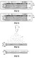
- the temperature process may also be performed in a reactor 5 which is illustrated in Figures 12 and 13 .
- the atmosphere 50 may be provided in a reactor 5.
- the atmosphere 50 may be inert.
- a suitable inert atmosphere may include, for instance, at least on of: nitrogen (N 2 ); argon (Ar); helium (He); neon (Ne); crypton (Kr); xenon (Xe).
- the respective surfaces 10t, 10b are coated directly with a copper-containing material 7. That is, the copper-containing material 7 forms the first copper-containing layer 21' on the first ceramic surface 10t so that the copper-containing material 7 adjoins the first ceramic surface 10t, and, if provided, the second copper-containing layer 22' on the second ceramic surface 10b so that the copper-containing material 7 adjoins the second ceramic surface 10b.
- the first copper-containing layer 21' is not attached in the form of a solid body (e.g.
- the second copper-containing layer 22' is not attached in the form of a solid body (e.g. in the form of a metal foil) to the second ceramic surface 10b because this would cause undesired voids formed between the first ceramic surface 10t and the solid body.
- the first copper-containing layer 21' may be formed on the first ceramic surface 10t by at least one of: depositing a copper-containing material 7 on the first ceramic surface 10t in a deposition process; applying a copper-containing material 7 to the first ceramic surface 10t, which is, when it initially contacts the first ceramic surface 10t, fluid.
- the second copper-containing layer 22' may be formed on the second ceramic surface 10b by at least one of: depositing a copper-containing material 7 on the second ceramic surface 10b in a deposition process; applying a copper-containing material 7 to the second ceramic surface 10b, which is, when it initially contacts the second ceramic surface 10b, fluid.
- depositing is to be understood in the sense of a deposition process, in which a copper-containing material 7 is deposited in the form of a plurality of atoms and/or molecules particles which are not part of a common solid body.
- a copper-containing material 7 may be successively deposited on the first ceramic surface 10t (i.e. by growing the first copper-containing layer 21' on the first ceramic surface 10t), and/or by applying a copper-containing material 7 in liquid form to the first ceramic surface 10t (i.e. by wet application). Applying the copper-containing material 7 in liquid form to the first ceramic surface 10t may take place such that the copper-containing material 7, when it firstly comes into contact with the first ceramic surface 10t, is already in a liquid state.
- the second copper-containing layer 22' may be formed on the second surface 20t by successively depositing a copper-containing material 7 on the second surface 20t (i.e. by growing the second copper-containing layer 22' on the second ceramic surface 10b), and/or by applying a copper-containing material 7 in liquid form to the second ceramic surface 10b. Applying the copper-containing material 7 in liquid form to the second ceramic surface 10b may take place such that the copper-containing material 7, when it firstly comes into contact with the second ceramic surface 10b, is in a liquid state. If the copper-containing material 7 is applied in liquid form to the respective surface 10t and/or 10b, using a copper-containing material 7 having a melting point below room temperature (20°C) may facilitate the application process.
- the copper-containing material 7 may be released from a source 6 and deposited on the respective first ceramic surface 10t and second ceramic surface 10b, respectively, which is schematically illustrated in Figure 14 .
- Depositing the copper-containing material 7 on the first ceramic surface 10t of the carrier 10, and, if desired, on the second ceramic surface 10b of the carrier 10 may take place by at least one of: physical vapour deposition (e.g. sputtering); and chemical vapour deposition.
- Suitable materials for physical vapour deposition are, for instance, copper, aluminium (Al); all noble metals (e.g. silver (Ag); gold (Au); Platinum (Pt)).
- Suitable materials for chemical vapour deposition are, for instance, copper, copper-containing alloys with at least 60% Cu, as well as all noble metals (Au, Ag, Pt,).
- the copper-containing material 7 may be a copper-containing solution which is applied to the respective first ceramic surface 10t and second ceramic surface 10b by at least one of: spraying the copper-containing solution 7 onto the respective surface 10t, 10b; dispensing the copper-containing solution 7 onto the respective surface 10t, 10b (see also Figure 14 ); and immersing the carrier 10 into the copper-containing solution 7 (see Figure 15 ).
- Suitable copper-containing solution may include, for instance, at least one of: copper(II) hydroxide; and copper(II) acetate.
- the carrier 10 may be placed in a low pressure atmosphere, for instance in an atmosphere having an absolute pressure of less than 90% of the pressure of the ambient atmosphere, in order to avoid gas-filled voids between the respective surface 10t, 10b and the copper-containing solution 7 applied thereto.
- a copper-containing layer 21', 22' may be produced on the respective surface 10t, 10b using only one or, alternatively, at least two of the methods mentioned above. In the latter case, any of the at least two methods may be combined with one another. Thereby, the at least two methods may be executed in any order.
- the respective final copper-containing layer 21', 22' includes a copper-containing first sub-layer which results from the method executed first and which directly contacts the respective surface 10t, 10b, a copper-containing second sub-layer which results from the method executed secondly and which directly contacts the first sub-layer so that the first sub-layer is disposed between the respective surface 10t, 10b and the second sub-layer, an optional copper-containing third sub-layer which results from the method executed thirdly and which directly contacts the second sub-layer so that the second sub-layer is disposed between the first sub-layer and the third sub-layer, and so on. That is, the respective copper-containing layer 21', 22' may be a stack composed of at least two copper-containing sub-layers.
- the number of sub-layers is identical to the number of the (subsequently executed) at least two methods.
- the liquid copper-containing material 7 applied in the one of the at least two methods may be dried prior to executing the other one of the at least two methods.
- first copper-containing layer 21' to be produced on the first ceramic surface 10t and a second copper-containing layer 22' to be produced on the second ceramic surface 10b
- producing the second copper-containing layer 22' on the second ceramic surface 10b may take place, irrespective of the method used, prior to, simultaneously with or after producing the first copper-containing layer 21' on the first ceramic surface 10t. It is also possible that copper-containing sub-layers are produced alternatingly on the first and second ceramic surfaces 10t, 10b.
- the pre-fabricated copper-containing first metal foil 11 may be directly attached to the completed first copper-containing layer 21' such that the first metal foil 11 adjoins a copper-containing material 7 that has been applied to the carrier 10 with one of the methods described above. If the completed first copper-containing layer 21' includes two or more sub-layers, the first metal foil 11 adjoins that one of those sub-layers that has been produced at last. Accordingly, the pre-fabricated copper-containing first metal foil 11, if provided, may be directly attached to the completed second copper-containing layer 22' such that the second metal foil 12 adjoins a copper-containing material 7 that has been applied to the carrier 10 with one of the methods described above. If the completed second copper-containing layer 22' includes two or more sub-layers, the second metal foil 12 adjoins that one of those sub-layers that has been produced at last.
- a copper-containing liquid e.g. a copper-containing solution
- the applied copper-containing liquid is to be dried prior to placing the first metal foil 11 on the dried copper-containing "liquid" (which is equal to the dry first copper-containing layer 21')
- a copper-containing liquid is used as the copper-containing material 7 applied to the second ceramic surface 10b
- the applied copper-containing liquid is to be dried prior to placing the second metal foil 12 on the dried copper-containing "liquid” (which is equal to the dry second copper-containing layer 22'). Drying may optionally take place in a furnace 5' as illustrated in Figure 16 . It is to be noted that the above-mentioned layer thicknesses d21', d22' relate to the dried copper-containing layers 21' and 22', respectively.
- the copper-containing first foil 11 was joined to the first ceramic surface 10t of the carrier 10, and, simultaneously, the copper-containing second foil 12 was joined to the second surface 10b of the carrier 10.
- each of the first and second temperature processes may include a heating process and a subsequent cooling process using the same parameters as described above.
- each of the first and/or second metal foils 11, 12 may optionally be structured to include conductive lines.
- structuring may take place prior to joining the respective metal foil 11, 12 with the carrier 10, for instance by stamping, or after joining the respective metal foil 11, 12 with the carrier 10, for instance by masked etching.
- FIG. 17 illustrates various steps of a method for producing a circuit board.
- the methods explained with reference to Figures 17 to 19 differ in the order of the steps.
- the carrier 10 is provided (step a).
- the first copper-containing layer 21' is produced on the first ceramic surface 10t (step b) and, subsequently, the first metal foil 11 is placed on the applied first copper-containing layer 21' (step c).
- the first metal foil 11, the first copper-containing layer 21' and the carrier 10 are joined in heating process and a subsequent cooling process as described above, whereby the first metal foil 11 and the first copper-containing layer 21' unify and form the first metallisation 61.
- the second copper-containing layer 22' is produced on the second ceramic surface 10b (step d) and, subsequently, the second metal foil 12 is placed on the applied second copper-containing layer 22' (step e). Subsequently, the second metal foil 12, the second copper-containing layer 22' and the carrier 10 are joined in a heating process and a subsequent cooling process as described above, whereby the second metal foil 12 and the second copper-containing layer 22' unify and form the second metallisation 62 (step f).
- the carrier 10 is provided (step a). Then, the first copper-containing layer 21' is produced on the first ceramic surface 10t and the second copper-containing layer 22' is produced on the second ceramic surface 10b (step b). Subsequently, the first metal foil 11 is placed on the applied first copper-containing layer 21' (step c). Subsequently, the first metal foil 11, the first copper-containing layer 21' and the carrier 10 are joined in a heating process and a subsequent cooling process as described above, whereby the first metal foil 11 and the first copper-containing layer 21' unify and form the first metallisation 61 (step d). Subsequently, the second metal foil 12 is placed on the applied second copper-containing layer 22' (step e).
- the second metal foil 12, the second copper-containing layer 22' and the carrier 10 are joined in a heating process and a subsequent cooling process as described above, whereby the second metal foil 12 and the second copper-containing layer 22' unify and form the second metallisation 62 (step f).
- the carrier 10 is provided (step a). Then, the first copper-containing layer 21' is produced on the first ceramic surface 10t and the second copper-containing layer 22' is produced on the second ceramic surface 10b (step b). Subsequently, the first metal foil 11 is placed on the applied first copper-containing layer 21', and the second metal foil 12 is placed on the applied second copper-containing layer 22' (step c).
- the first metal foil 11, the first copper-containing layer 21' and the carrier 10 are joined, whereby the first metal foil 11 and the first copper-containing layer 21' unify and form the first metallisation 61, and the second metal foil 12, the second copper-containing layer 22' and the carrier 10 are joined, whereby the second metal foil 12 and the second copper-containing layer 22' unify and form the second metallisation 62 (step d).
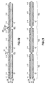
- Figure 20 shows a panel with several circuit boards.
- the panel may be formed in the same manner as one of the circuits boards described above.
- the carrier 10, the first metal foil 11 and the second metal foil 12 are common to all circuit boards.
- the first metal foil 11 and the second metal foil 12 are, for instance during the mentioned masked etching process, structured such that the carrier 10 is exposed at opposing first sections 15b and second sections 15t of the carrier 10.
- the sections 15t are sections of the first ceramic surface 10t
- the sections 15b are sections of the second ceramic surface 10b.
- a laser beam 300 produces scores 301 in the carrier 10 so that the circuit boards can easily be singulated by breaking the carrier 10 along the scores 301.
- Figure 21 shows the singulated circuit boards 100.
Landscapes
- Chemical & Material Sciences (AREA)
- Engineering & Computer Science (AREA)
- Ceramic Engineering (AREA)
- Materials Engineering (AREA)
- Structural Engineering (AREA)
- Organic Chemistry (AREA)
- Manufacturing & Machinery (AREA)
- Microelectronics & Electronic Packaging (AREA)
- Manufacturing Of Printed Wiring (AREA)
Abstract
One aspect relates to a method for producing a circuit board. A copper-containing metal foil 11, 12 is disposed on a copper and oxygen containing coating 21', 22' of a carrier 10 so that the coating adjoins both the metal foil 11, 12 and a ceramic surface 10t, 10b of the carrier. The carrier, the coating and the metal foil are heated to at least a first temperature so that the coating and the metal foil unify, under the formation of a copper and oxygen containing eutectic, to a metallization layer. Subsequently, the carrier and the metallization layer are cooled to temperatures below the first temperature.
Description
- The instant disclosure relates to a circuit board and to a method for producing a circuit board.
- Many electronic devices as, for instance, power semiconductor modules, employ metallised carriers as circuit boards for carrying one or more power semiconductor chips because they have a high thermal conductivity for dissipating heat from the power semiconductor chip(s), a coefficient of thermal expansion that does not differ too greatly from the coefficient of thermal expansion of usual power semiconductor chips, and a high dielectric strength. As the metallisation of the metallised carrier is used to provide electrically conducting paths, it often includes copper because the high electrical and thermal conductivity of copper is favourable for achieving both a high ampacity and good heat spreading properties. In order to produce such circuit boards, pre-fabricated, copper-containing metal foils are directly attached to the carrier at high temperatures. This process is also known as DCB-process (DCB = direct copper bonding). However, due to an unavoidable unevenness of pre-fabricated, copper-containing metal foils and carriers, conventional methods for producing such a circuit board suffer from gas-filled voids at the interface between the carrier and the metallisation. When high electric voltages are applied to the circuit board, a partial discharge may occur in the gas-filled voids, causing damage to the circuit board.
- Hence, there is a general need for a method for producing a circuit board that has a copper-containing metallisation attached to a carrier and that has a high partial discharge resistance.
- One aspect relates to a method for producing a circuit board. A copper-containing metal foil is disposed on a copper and oxygen containing coating of a carrier so that the coating adjoins both the metal foil and a ceramic surface of the carrier. The carrier, the coating and the metal foil are heated to at least a first temperature so that the coating and the metal foil unify, under the formation of a copper and oxygen containing eutectic, to a metallization layer. Subsequently, the carrier and the metallization layer are cooled to temperatures below the first temperature.
- A further aspect relates to a circuit board comprising a copper-containing metallisation formed on a ceramic surface of a carrier, wherein there is no gas-filled void that is directly bounded by both the copper-containing metallisation and the ceramic surface and has, in a direction perpendicular to a plane, which is tangent to at least three different, non-linear points of the ceramic surface but does not intersect the carrier, a maximum dimension of more than 30 µm.
- Examples are explained below with reference to the drawings. The drawings serve to illustrate certain principles, so that only aspects necessary for understanding these principles are illustrated. The drawings are not to scale. In the drawings the same reference characters denote like features.
-
-
Figures 1 to 7 are cross-sectional views illustrating several steps of producing a circuit board having a carrier. -
Figure 8 is a cross-sectional view illustrating an enlarged section A of the circuit board ofFigure 7 . -
Figure 9 is a cross-sectional view illustrating an enlarged section B of the circuit board ofFigure 7 -
Figure 10 is a cross-sectional view illustrating a circuit board having a structured metallisation. -
Figure 11 is a cross-sectional view illustrating the circuit board after being equipped with a semiconductor chip. -
Figure 12 is a cross-sectional view illustrating the heating of the carrier, the copper-containing foil and the copper-containing layer in a heating process to temperatures of at least 1065°C. -
Figure 13 is a cross-sectional view illustrating the cooling of the heated carrier and the cooling of a metallisation formed from the copper-containing foil and the copper-containing layer in a cooling process to temperatures of less than 1065°C. -
Figure 14 is a cross-sectional view illustrating the production of a copper-containing layer on a carrier by spraying a copper-containing solution onto the carrier. -
Figure 15 is a cross-sectional view illustrating the production of a copper-containing layer on a carrier by immersing the carrier into a copper-containing solution. -
Figure 16 is a cross-sectional view illustrating the drying of the copper-containing solution applied to the carrier. -
Figure 17 illustrates various steps of a method for producing a circuit board according to a first example. -
Figure 18 illustrates various steps of a method for producing a circuit board according to a second example. -
Figure 19 illustrates various steps of a method for producing a circuit board according to a first example. -
Figures 20 and 21 are cross-sectional views illustrating how a number of circuit boards may be produced simultaneously and subsequently singulated. - In the following detailed description, reference is made to the accompanying drawings. The drawings form a part of the description and by way of illustration show specific examples in which the invention may be practised. It is to be understood that the features of the various examples described herein may be combined with each other, unless specifically noted otherwise.
-
Figure 1 schematically illustrates anexemplary carrier 10 having a firstceramic surface 10t, and, asecond surface 10b opposite the firstceramic surface 10t. Optionally, thesecond surface 10b may be a ceramic surface. Thecarrier 10 may be a flat platelet with the firstceramic surface 10t and thesecond surface 10b being plane parallel and having a layer thickness d10. For instance, the layer thickness d10 may be 0.2 to 1 mm. However, a thickness d10 of less than 0.2 or of more than 1 is also applicable. Thecarrier 10 may consist of or at least comprise ceramic. Optionally, thecarrier 10 may be a ceramic carrier, i.e. a carrier that consists of ceramics. - Suitable ceramic materials forming a
ceramic carrier 10 or at least the firstceramic surface 10t and, optionally, the secondceramic surface 10b, are, for example, oxides like aluminium oxide, magnesium oxide, uranium oxide, zirconium oxide, or zinc oxide. Alternatively, any carrier, the ceramic of which can be oxidised, e.g. magnesium aluminate or barium titanate or aluminium nitride carrier or silicon nitride, may be used ascarrier 10 or to at least form the firstceramic surface 10t and, optionally, the secondceramic surface 10b. - As illustrated in
Figure 2 , a dry first copper-containinglayer 21' having a layer thickness d21' is formed on the firstceramic surface 10t of thecarrier 10 in order to subsequently attach a pre-fabricated copper-containing first metal foil 11 (seeFigure 3 ) to the firstceramic surface 10t of thecarrier 10. The first copper-containinglayer 21' forms a coating of thecarrier 10. The pre-fabricated copper-containing first metal foil 11 (seeFigure 3 ) may consist of copper or contain at least 60 atom% (atom percent) copper and has a layer thickness d11. The layer thickness d21' of the first copper-containinglayer 21' may be, for instance, selected from a range from 0.1 µm to 10 µm. However, a thickness d10 of less than 0.1 µm or of more than 10 µm is also applicable. The layer thickness d11 of thefirst metal foil 11 may be, for instance, selected from a range from 0.1 mm to 1 mm. However, a thickness d11 of less than 0.1 mm or of more than 1 mm is also applicable. - After forming the first copper-containing
layer 21' on the firstceramic surface 10t of thecarrier 10, the pre-fabricatedfirst metal foil 11 is placed on the first copper-containinglayer 21' so that the first copper-containinglayer 21' is disposed between thecarrier 10 and thefirst metal foil 11 and adjoins both the firstceramic surface 10t of thecarrier 10 and thesurface 11b of thefirst metal foil 11. - The first copper-containing
layer 21' contains a chemical element or composition that includes and/or can be converted into at least one copper oxide, e.g. into at least one of CuO, Cu2O, CuO2, CuO3, by heating the first copper-containinglayer 21' in a heating process to high temperatures, for instance to temperatures of at least 70°C, e.g. to temperatures of 100°C to 150°C. By further heating the first copper-containinglayer 21' with thefirst metal foil 11 attached to it so that the copper-containinglayer 21' adjoins both the firstceramic surface 10t and thefirst metal foil 11, for instance to at least 200°C in a reductive or inert atmosphere, the copper oxide is reduced to metallic copper so that the metallic copper contained in the first copper-containinglayer 21' forms a copper layer that is in close contact with the firstceramic surface 10t of thecarrier 10 so that there exist no or no substantial gas-filled voids 9 (seeFigure 9 ) between the copper layer and the firstceramic surface 10t. Industrially, this reduction may be performed, for instance, in a reduction process by heating thecarrier 10, the first copper-containing layer 21'applied to the firstceramic surface 10t and thefirst foil 11 with the first copper-containing layer 21'disposed between and adjoining both the firstceramic surface 10t and thefirst foil 11 in a furnace to temperatures of more than 1000°C under an inert atmosphere, where the copper oxide dissociates into metallic copper (Cu) and gaseous oxygen (O2). Depending on the duration of the reduction process and the temperature used in the reduction process, the dissociation can be complete so that substantially all of the copper oxide is dissociated. The degree of dissociation increases with the duration and the temperature used in the reduction process. - As illustrated in
Figure 4 , thecarrier 10 with the first copper-containinglayer 21' attached to the firstceramic surface 10t may optionally be placed on anauxiliary carrier 100, and thefirst metal foil 11 may be placed on the first copper-containinglayer 21' applied to the firstceramic surface 10t so that the first copper-containinglayer 21' is in physical contact with thefirst foil 11, disposed between and in physical contact with both the firstceramic surface 10t of thecarrier 10 and thefirst metal foil 11. - In the same manner, an optional pre-fabricated copper-containing second metal foil 12 (see
Figure 3 ) having a layer thickness d12 may be attached to thesecond surface 10b of thecarrier 10 using a dry second copper-containing layer 22' which forms a coating of thecarrier 10. For this, the second copper-containing layer 22', which may consist of copper or contain at least 60 atom% (atom percent) copper and has a layer thickness d22', is formed on thesecond surface 10b of thecarrier 10 which. Because there is asecond metal foil 12 attached to thesecond surface 10b, thesecond surface 10b is a ceramic surface. The layer thickness d22' of the second copper-containing layer 22' may be, for instance, selected from a range of 0.1 µm to 10 µm. The layer thickness d12 of thesecond metal foil 12 may be, for instance, selected from a range of 0.1 mm to 1 mm. However, a thickness d12 of less than 0.1 mm or of more than 1 mm is also applicable. It is to be noted that the layer thicknesses d10, d11, d12, d21 and d22 may be selected independently from one another. If there is no optionalsecond metal foil 12 to be attached to the secondceramic surface 10b of thecarrier 10, the second copper-containing layer 22' and thesecond metal foil 12 may be omitted. - If there is, as schematically illustrated in
Figures 2 to 4 , a pre-fabricated second copper-containingmetal foil 11 to be attached to the secondceramic surface 10b of thecarrier 10, the second copper-containing layer 22' is formed on the secondceramic surface 10b of thecarrier 10, and, subsequently, the pre-fabricated second copper-containingmetal foil 12 is placed on the second copper-containing layer 22' so that the second copper-containing layer 22' is disposed between thecarrier 10 and the second copper-containingmetal foil 12 and adjoins both the secondceramic surface 10b of thecarrier 10 and thesurface 12t of the second copper-containingmetal foil 12, and that thecarrier 10 is disposed between the first copper-containinglayer 21' and the second copper-containing layer 22', and between the first copper-containingmetal foil 11 and the second copper-containingmetal foil 12. - In this state, as schematically illustrated in
Figure 5 , thecarrier 10, thefirst metal foil 11, the first copper-containinglayer 21', and, if provided, thesecond metal foil 12 and the second copper-containing layer 22' are heated in the heating process to temperatures of at least a minimum temperature, e.g. 1065°C, so that the first copper-containinglayer 21' and thefirst metal foil 11 unify and form thefirst metallisation 61, and if provided, so that the second copper-containing layer 22' and thesecond metal foil 12 unify and form thesecond metallisation 62. In that heating process, at least one eutectic phase, which may consist of or comprise a copper-oxygen-eutectic, occurs. - After the heating process, the
carrier 10, thefirst metallisation 61 and, if provided, thesecond metallisation layer 62 are, as schematically illustrated inFigure 6 , cooled down to temperatures of less than the minimum temperature, for instance to temperatures of less than 50°C, e.g. to room temperature (20°C), in a cooling process. Prior to and/or during the mentioned heating process and the subsequent cooling process, copper contained in the chemical composition of the first copper-containinglayer 21' and, if provided, the second copper-containing layer 22' is converted into at least one copper oxide (e.g. into at least one of CuO; Cu2O; CuO2; Cu2O3) and then reduced to metallic copper so that from copper contained in the first copper-containinglayer 21', the first copper layer is joined with both the firstceramic surface 10t of thecarrier 10 and thefirst metal foil 11, and, if there is also a second copper-containing layer 22', from copper contained in the second copper-containing layer 22', a second copper layer is formed that is joined with both the secondceramic surface 10b of thecarrier 10 and thesecond metal foil 12. - During the heating process, the
first metal foil 11 and the first copper-containinglayer 21' unify so that they form afirst metallisation 61 adjoining the firstceramic surface 10t. Thefirst metallisation 61 may include layers having different materials or different material compositions emanating fromfirst metal foil 11 and the first copper-containinglayer 21', but it is also possible that thefirst metallisation layer 61 is fully alloyed so that it has a homogeneous material or material composition. Accordingly, when there is asecond metal foil 12 joined to the secondceramic surface 10b of thecarrier 10, thesecond metal foil 12 and the second copper-containing layer 22' unify during the heating process so that they form asecond metallisation 62 adjoining the secondceramic surface 10b. Thesecond metallisation 62 may include layers having different materials or different material compositions emanating fromsecond metal foil 12 and the second copper-containing layer 22', but it is also possible that thesecond metallisation layer 62 is fully alloyed so that it has a homogeneous material or material composition. - Optionally, a
weight 200 may be placed on that side of thefirst metal foil 11 facing away from thecarrier 10 during the heating process so that potential gas-filled voids 9 (Figure 9 ) forming between the first copper-containinglayer 21' and the firstceramic surface 10t and/or between the second copper-containing layer 22' and the secondceramic surface 10b are kept small. However, a pressure P that is exerted on the firstceramic surface 10t during the mentioned heating and cooling processes may be low and can therefore be generated without requiring expensive equipment. Therefore, the heating process and the subsequent cooling process may optionally be carried out with non-isostatic pressing. Nevertheless, hot isostatic pressing (HIP) may alternatively be used. For instance, the heating process and the subsequent cooling process may be carried out such that after one of thecarrier 10, the copper-containingmetal foil 11 and the copper-containinglayer 21' has reached a temperature of at least 1065°C in the heating process and before each of the first copper-containinglayer 21', thecarrier 10 and themetallisation 61 has reached a temperature of less than 1065°C in the cooling process, a pressure P exerted on the firstceramic surface 10t does not exceed 30 MPa. However, it is to be noted that from a technical point of view, a pressure P higher than 30 MPa may be used as well. For instance, the heating process and the subsequent cooling process may be carried out hot isostatic pressing (HIP). - Independently of whether the pressure P is selected to exceed 30 MPa or not, it may be generated in a random manner, for instance using a weight 200 (in this case the pressure P is caused by the total combined weight of the
weight 200, the self-weight of thefirst metal foil 11 and the self-weight of the copper-containinglayer 21' or, from a later stage of the heating process on, by the total combined weight of theweight 200 and the self-weight of the first metallisation 61), or even without the weight 200 (in this case the pressure P is caused by the total combined weight of the self-weight of thefirst metal foil 11 and the self-weight of the copper-containinglayer 21' or, from a later stage of the heating process on, by the self-weight of the first metallisation 61), but also using a press or by hot isostatic pressing. -
Figure 7 illustrates thecarrier 10 provided with thefirst metallisation 61 and thesecond metallisation 62 after the removal of theauxiliary carrier 100 and theweight 200. - As can be seen from
Figure 8 which illustrates an enlarged section A of the circuit board ofFigure 7 , gas-filled voids 8 (emanating from an ambient atmosphere when thefirst metal foil 11 was placed on the first copper-containinglayer 21') are disposed distant from the firstceramic surface 10t and therefore fully enclosed by metal. Therefore, an electric field inside the gas-filledvoids 8 is zero so that an electrical field applied to the gas-filledvoids 8 cannot cause a partial discharge in the region of the gas-filledvoids 8. The gas-filledvoids 8 are disposed distant from the firstceramic surface 10t because the copper-containinglayer 21' was applied to the firstceramic surface 10t prior to placing thefirst metal foil 11 on the applied copper-containinglayer 21'. Analogously, gas-filled voids emanating from an ambient atmosphere when thesecond metal foil 12 was placed on the second copper-containing layer 22' are disposed distant from the secondceramic surface 10b and therefore fully enclosed by metal. - As further shown in
Figure 9 which illustrates an enlarged section B of the circuit board ofFigure 7 , small gas-filledvoids 9 may happen to occur between the firstceramic surface 10t and thefirst metallisation 61. Different from the gas-filledvoids 8 explained with reference toFigure 8 , the gas-filledvoids 9 are not fully enclosed by metal. Instead, they are directly bounded by both thefirst metallisation 61 and the firstceramic surface 10t of thecarrier 10. That is, for each point P9 inside of a gas-filledvoid 9 there is at least one first continuous path a running only through the gas inside the gas-filledvoid 9 from that point P9 to the firstceramic surface 10t, and at least one second continuous path b running only through the gas inside the gas-filledvoid 9 from that point P9 to thefirst metallisation 61. - The problem of partial discharge caused by an electric field affecting a gas-filled
void 9 can be reduced by keeping the maximum dimension the gas-filledvoid 9 has in the direction of the electric field low. Further, in many applications, an electrical field that might cause partial discharge at a gas-filledvoid 9 runs substantially perpendicular to the firstceramic surface 10t. With the present invention, gas-filledvoids 9, if any, having low maximum dimensions in the direction perpendicular to the firstceramic surface 10t can be achieved. - As illustrated in
Figure 9 , a plane E can be defined which is tangent to at least three different, non-linear points P1, P2, P3 of thesurface 10t of thecarrier 10 and which does not intersect thecarrier 10. It is to be noted that the reference line for point P3 is illustrated in dashed fashion in order to express that P3 is not located in the sectional plane ofFigure 9 . In acircuit board 100 of the present invention, first applying the copper-containinglayer 21' to the firstceramic surface 10t and then placing thefirst metal foil 11 on the applied, copper-containinglayer 21' allows for the production of acircuit board 100 in which there is no gas-filledvoid 9 that is directly bounded by both thefirst metallisation 61 and the firstceramic surface 10t of thecarrier 10 and that has, in a direction perpendicular to the plane E, a maximum dimension d9max of more than 30 µm or even of more than 10 µm. - A further option for keeping potential gas-filled voids 9 (
Figure 9 ) from forming between the firstceramic surface 10t and thefirst metallisation 61 and/or, analogously, between the secondceramic surface 10b and thesecond metallisation 62 small is to ensure that therespective surfaces carrier 10 are smooth so that no gas-filledvoids 9 or at least no large gas-filledvoids 9 are produced between the firstceramic surface 10t and the copper-containinglayer 21' and/or, analogously, between the secondceramic surface 10b and the copper-containing layer 22', when a copper-containing material for producing the copper-containing layer(s) 21', 22' is applied to therespective surface smooth surfaces 10t and/or 10b may be achieved by at least one of polishing and lapping. - Another additional or alternative option that can help prevent such potential gas-filled
voids 9 or at least keep such potential gas-filledvoids 9 small is to ensure that therespective surfaces carrier 10 are, prior to applying the respective copper-containinglayer 21', 22' to therespective surface voids 9. Organic particles may be removed from the firstceramic surface 10t and the secondceramic surface 10b by heating thecarrier 10, prior to applying a copper-containing material forming the respective copper-containinglayer 21', 22' to therespective surface carrier 10 to temperatures of at least 400°C, thecarrier 10, which may be a fired green compact, may be subject to a pre-cleaning process, in which undesired remainders sticking to thecarrier 10 are removed. Such remainders may be, for instance, abrasive dust resulting from polishing and/or lapping thecarrier 10 at at least one of thesurfaces 10t and/or 10b, an abherent like boron nitride (BN) that allows for separating thecarrier 10 after the firing of the green compact from adjacent parts (e.g. from a pressing tool or from a further green compact fired commonly with the carrier 10) used in the firing process, or any other remainder. Optionally, thecarrier 10 may have, after the pre-cleaning process but prior to heating it to temperatures of at least 400°C, a temperature of less than 100°C or even less than 50°C. Further, the pre-cleaning process may include mechanically cleaning thecarrier 10, for instance by flushing thecarrier 10 using a cleaning fluid (e.g. a liquid like water or a solvent, or a gas stream like an air stream). - The heating temperature process, in which the
carrier 10, thefirst metal foil 11, the first copper-containinglayer 21', and, if provided, thesecond metal foil 12 and the second copper-containing layer 22' are heated to temperatures of at least 1065°C, and the subsequent cooling process, in which thefirst metallisation 61 and (in case of a previoussecond metal foil 12 and a previous second copper-containing layer 22') are cooled to temperatures of less than 1065°C may be carried out such that the temperatures of at least 1065°C do not exceed the melting point(s) of thefirst metal foil 11 and thefirst metallisation 61, and, if provided, the melting point(s) of thesecond metal foil 12 and thesecond metallisation 62. Not exceeding a temperature of 1083°C during the heating process and the subsequent cooling process ensures that both the heating process and the cooling process are carried out at temperatures below the melting point of copper. - During the heating process and the subsequent cooling process, tight bonds between the
carrier 10 and both the first metal foil 11 (i.e. between the firstceramic surface 10t and the first metallisation 61) and (if provided) the second metal foil 12 (i.e. between the secondceramic surface 10b and the second metallisation 62) are produced. - Then, if desired, the
first metallisation 61 may be structured to include an arbitrary number and an arbitrary pattern of electrically conductinglines Figure 10 . For structuring, any conventional technique may be used. One suitable technique is, for example, masked etching of thefirst metallisation 61. - As further illustrated in
Figure 11 , thecircuit board 100 may, after the mentioned cooling process, be equipped with at least onepower semiconductor chip 3. Thepower semiconductor chip 3 is attached to thefirst metal foil 11 using a connection layer 4, for instance a solder, a sintered metal powder (e.g. a sintered silver powder), or an electrically conductive or electrically insulating adhesive. The connection layer 4 adjoins both thefirst metal foil 11 and thepower semiconductor chip 3. - The
power semiconductor chip 3 may include a semiconductor body 40 with a semiconductor component that has a load path formed between afirst chip metallisation 31 and a second chip metallisation 32. Each of thefirst chip metallisation 31 and the second chip metallisation 32 is disposed on a surface of thesemiconductor body 30. The semiconductor component may be, for instance, a diode, or a controllable semiconductor component like a unipolar or bipolar transistor or a thyristor. In case of a transistor, the controllable semiconductor component may be, for instance, an IGFET (Insulated Gate Bipolar Transistor) like a MOSFET (Metal Oxide Semiconductor Field-Effect Transistor) or an IGBT (Insulated Gate Bipolar Transistor), a JFET (Junction Field Effect Transistor), a HEMT (High Electron Mobility Transistor), a BJT (Bipolar Junction Transistor), or any other transistor. - The
first chip metallisation 31 and the second chip metallisation 32 may be, for instance, a source metallisation and a drain metallisation, or a drain metallisation and a source metallisation, or an emitter metallisation and a collector metallisation, or a collector metallisation and an emitter metallisation, or an anode metallisation and a cathode metallisation, or a cathode metallisation and an anode metallisation. The semiconductor component may optionally be a vertical semiconductor component with thefirst chip metallisation 31 and the second chip metallisation 32 disposed on opposite surfaces of the semiconductor body 40. - In case of a controllable semiconductor component, the semiconductor chip 4 has a
third chip metallisation 33. Thethird chip metallisation 33 is disposed on a surface of thesemiconductor body 30, for instance on a surface facing away from thefirst metal foil 11, or on a surface of thesemiconductor body 30 facing toward thefirst metal foil 11. The third chip metallisation may be, for instance, a gate metallisation or a base metallisation. - The mentioned temperature process (see also
Figures 5 and 6 ) may optionally take place under ambient conditions. Alternatively, the temperature process may also be performed in areactor 5 which is illustrated inFigures 12 and 13 . Here, heating thecarrier 10, thefirst metal foil 11 and the first copper-containinglayer 21' and, if provided, thesecond metal foil 12, the second copper-containing layer 22', to temperatures of at least 1065°C (Figure 12 , which already shows thefirst metal foil 11 and the first copper-containinglayer 21' unified to thefirst metallisation 61 and thesecond metal foil 12 and the second copper-containing layer 22' unified to the first metallisation 61) and, optionally, the subsequent cooling process in which the mentioned parts are cooled down to temperatures below 1065°C, takes place in anatmosphere 50 surrounding the mentioned parts and fulfilling at least one of the following conditions: an absolute pressure of more than 0.8106 bar and less than 1.01325 bar; and an oxygen content of at most 5 atom percent. Theatmosphere 50 may be provided in areactor 5. Optionally, theatmosphere 50 may be inert. A suitable inert atmosphere may include, for instance, at least on of: nitrogen (N2); argon (Ar); helium (He); neon (Ne); crypton (Kr); xenon (Xe). - In order to form the first copper-containing
layer 21' on the firstceramic surface 10t of thecarrier 10, and, optionally, to form the second copper-containing layer 22' on the secondceramic surface 10b of the carrier 10 (which is illustrated inFigure 2 ), therespective surfaces material 7. That is, the copper-containingmaterial 7 forms the first copper-containinglayer 21' on the firstceramic surface 10t so that the copper-containingmaterial 7 adjoins the firstceramic surface 10t, and, if provided, the second copper-containing layer 22' on the secondceramic surface 10b so that the copper-containingmaterial 7 adjoins the secondceramic surface 10b. As will be explained below in more detail, the first copper-containinglayer 21' is not attached in the form of a solid body (e.g. in the form of a metal foil) to the firstceramic surface 10t because this would cause undesired voids formed between the firstceramic surface 10t and the solid body. Accordingly, the second copper-containing layer 22', if provided, is not attached in the form of a solid body (e.g. in the form of a metal foil) to the secondceramic surface 10b because this would cause undesired voids formed between the firstceramic surface 10t and the solid body. - Instead, the first copper-containing
layer 21' may be formed on the firstceramic surface 10t by at least one of: depositing a copper-containingmaterial 7 on the firstceramic surface 10t in a deposition process; applying a copper-containingmaterial 7 to the firstceramic surface 10t, which is, when it initially contacts the firstceramic surface 10t, fluid. Accordingly, the second copper-containing layer 22' may be formed on the secondceramic surface 10b by at least one of: depositing a copper-containingmaterial 7 on the secondceramic surface 10b in a deposition process; applying a copper-containingmaterial 7 to the secondceramic surface 10b, which is, when it initially contacts the secondceramic surface 10b, fluid. In this sense, "depositing" is to be understood in the sense of a deposition process, in which a copper-containingmaterial 7 is deposited in the form of a plurality of atoms and/or molecules particles which are not part of a common solid body. - According to one example for forming the first copper-containing
layer 21' on the firstceramic surface 10t, a copper-containingmaterial 7 may be successively deposited on the firstceramic surface 10t (i.e. by growing the first copper-containinglayer 21' on the firstceramic surface 10t), and/or by applying a copper-containingmaterial 7 in liquid form to the firstceramic surface 10t (i.e. by wet application). Applying the copper-containingmaterial 7 in liquid form to the firstceramic surface 10t may take place such that the copper-containingmaterial 7, when it firstly comes into contact with the firstceramic surface 10t, is already in a liquid state. Accordingly, the second copper-containing layer 22', if provided, may be formed on the second surface 20t by successively depositing a copper-containingmaterial 7 on the second surface 20t (i.e. by growing the second copper-containing layer 22' on the secondceramic surface 10b), and/or by applying a copper-containingmaterial 7 in liquid form to the secondceramic surface 10b. Applying the copper-containingmaterial 7 in liquid form to the secondceramic surface 10b may take place such that the copper-containingmaterial 7, when it firstly comes into contact with the secondceramic surface 10b, is in a liquid state. If the copper-containingmaterial 7 is applied in liquid form to therespective surface 10t and/or 10b, using a copper-containingmaterial 7 having a melting point below room temperature (20°C) may facilitate the application process. - According to an example, in which the copper-containing
layer 21' and 22' are grown on therespective surfaces material 7 may be released from asource 6 and deposited on the respective firstceramic surface 10t and secondceramic surface 10b, respectively, which is schematically illustrated inFigure 14 . Depositing the copper-containingmaterial 7 on the firstceramic surface 10t of thecarrier 10, and, if desired, on the secondceramic surface 10b of thecarrier 10 may take place by at least one of: physical vapour deposition (e.g. sputtering); and chemical vapour deposition. Suitable materials for physical vapour deposition (including sputtering) are, for instance, copper, aluminium (Al); all noble metals (e.g. silver (Ag); gold (Au); Platinum (Pt)). Suitable materials for chemical vapour deposition are, for instance, copper, copper-containing alloys with at least 60% Cu, as well as all noble metals (Au, Ag, Pt,...). - According to an example, in which the copper-containing
layer 21' and 22' are applied to therespective surfaces material 7 may be a copper-containing solution which is applied to the respective firstceramic surface 10t and secondceramic surface 10b by at least one of: spraying the copper-containingsolution 7 onto therespective surface solution 7 onto therespective surface Figure 14 ); and immersing thecarrier 10 into the copper-containing solution 7 (seeFigure 15 ). Suitable copper-containing solution may include, for instance, at least one of: copper(II) hydroxide; and copper(II) acetate. However, other copper-containing solutions that contain copper which can be converted into copper oxide may be used as well. During and/or after applying the copper-containingsolution 7 to the respective firstceramic surface 10t and/or secondceramic surface 10b, thecarrier 10 may be placed in a low pressure atmosphere, for instance in an atmosphere having an absolute pressure of less than 90% of the pressure of the ambient atmosphere, in order to avoid gas-filled voids between therespective surface solution 7 applied thereto. - It should be noted that a copper-containing
layer 21', 22' may be produced on therespective surface layer 21', 22' includes a copper-containing first sub-layer which results from the method executed first and which directly contacts therespective surface respective surface layer 21', 22' may be a stack composed of at least two copper-containing sub-layers. The number of sub-layers is identical to the number of the (subsequently executed) at least two methods. As far as one of the at least two methods, which uses a liquid copper-containingmaterial 7, is followed by another one of the at least two methods, the liquid copper-containingmaterial 7 applied in the one of the at least two methods may be dried prior to executing the other one of the at least two methods. - If there is a first copper-containing
layer 21' to be produced on the firstceramic surface 10t and a second copper-containing layer 22' to be produced on the secondceramic surface 10b, producing the second copper-containing layer 22' on the secondceramic surface 10b may take place, irrespective of the method used, prior to, simultaneously with or after producing the first copper-containinglayer 21' on the firstceramic surface 10t. It is also possible that copper-containing sub-layers are produced alternatingly on the first and secondceramic surfaces - As will be apparent from the above explanations, the pre-fabricated copper-containing
first metal foil 11 may be directly attached to the completed first copper-containinglayer 21' such that thefirst metal foil 11 adjoins a copper-containingmaterial 7 that has been applied to thecarrier 10 with one of the methods described above. If the completed first copper-containinglayer 21' includes two or more sub-layers, thefirst metal foil 11 adjoins that one of those sub-layers that has been produced at last. Accordingly, the pre-fabricated copper-containingfirst metal foil 11, if provided, may be directly attached to the completed second copper-containing layer 22' such that thesecond metal foil 12 adjoins a copper-containingmaterial 7 that has been applied to thecarrier 10 with one of the methods described above. If the completed second copper-containing layer 22' includes two or more sub-layers, thesecond metal foil 12 adjoins that one of those sub-layers that has been produced at last. - If a copper-containing liquid (e.g. a copper-containing solution) is used as the copper-containing
material 7 applied to the firstceramic surface 10t, the applied copper-containing liquid is to be dried prior to placing thefirst metal foil 11 on the dried copper-containing "liquid" (which is equal to the dry first copper-containinglayer 21'), and if a copper-containing liquid is used as the copper-containingmaterial 7 applied to the secondceramic surface 10b, the applied copper-containing liquid is to be dried prior to placing thesecond metal foil 12 on the dried copper-containing "liquid" (which is equal to the dry second copper-containing layer 22'). Drying may optionally take place in a furnace 5' as illustrated inFigure 16 . It is to be noted that the above-mentioned layer thicknesses d21', d22' relate to the dried copper-containinglayers 21' and 22', respectively. - The above-described methods for producing copper-containing
layers 21', 22' allow for a continuous coating of therespective surface material 7 so that there occur no or no substantial gas-filled voids caused by gas that is unintentionally enclosed between thecarrier 10 and the respective copper layer resulting from the copper-containing layers 21'and 22', respectively. - In some of the examples described above, the copper-containing
first foil 11 was joined to the firstceramic surface 10t of thecarrier 10, and, simultaneously, the copper-containingsecond foil 12 was joined to thesecond surface 10b of thecarrier 10. However, it is also possible to first join the copper-containingfirst foil 11 to the firstceramic surface 10t of thecarrier 10 during a first temperature process, and subsequently join the copper-containingsecond foil 12 to thesecond surface 10b of thecarrier 10 during a second temperature process. Thereby, each of the first and second temperature processes may include a heating process and a subsequent cooling process using the same parameters as described above. - In the described method, each of the first and/or second metal foils 11, 12 may optionally be structured to include conductive lines. In each case, structuring may take place prior to joining the
respective metal foil carrier 10, for instance by stamping, or after joining therespective metal foil carrier 10, for instance by masked etching. - Each of
Figures 17 to 19 illustrates various steps of a method for producing a circuit board. The methods explained with reference toFigures 17 to 19 differ in the order of the steps. According to the example ofFigure 17 , thecarrier 10 is provided (step a). Then, the first copper-containinglayer 21' is produced on the firstceramic surface 10t (step b) and, subsequently, thefirst metal foil 11 is placed on the applied first copper-containinglayer 21' (step c). Subsequently, thefirst metal foil 11, the first copper-containinglayer 21' and thecarrier 10 are joined in heating process and a subsequent cooling process as described above, whereby thefirst metal foil 11 and the first copper-containinglayer 21' unify and form thefirst metallisation 61. Subsequently, the second copper-containing layer 22' is produced on the secondceramic surface 10b (step d) and, subsequently, thesecond metal foil 12 is placed on the applied second copper-containing layer 22' (step e). Subsequently, thesecond metal foil 12, the second copper-containing layer 22' and thecarrier 10 are joined in a heating process and a subsequent cooling process as described above, whereby thesecond metal foil 12 and the second copper-containing layer 22' unify and form the second metallisation 62 (step f). - According to the example of
Figure 18 , thecarrier 10 is provided (step a). Then, the first copper-containinglayer 21' is produced on the firstceramic surface 10t and the second copper-containing layer 22' is produced on the secondceramic surface 10b (step b). Subsequently, thefirst metal foil 11 is placed on the applied first copper-containinglayer 21' (step c). Subsequently, thefirst metal foil 11, the first copper-containinglayer 21' and thecarrier 10 are joined in a heating process and a subsequent cooling process as described above, whereby thefirst metal foil 11 and the first copper-containinglayer 21' unify and form the first metallisation 61 (step d). Subsequently, thesecond metal foil 12 is placed on the applied second copper-containing layer 22' (step e). Subsequently, thesecond metal foil 12, the second copper-containing layer 22' and thecarrier 10 are joined in a heating process and a subsequent cooling process as described above, whereby thesecond metal foil 12 and the second copper-containing layer 22' unify and form the second metallisation 62 (step f). - According to the example of
Figure 19 , thecarrier 10 is provided (step a). Then, the first copper-containinglayer 21' is produced on the firstceramic surface 10t and the second copper-containing layer 22' is produced on the secondceramic surface 10b (step b). Subsequently, thefirst metal foil 11 is placed on the applied first copper-containinglayer 21', and thesecond metal foil 12 is placed on the applied second copper-containing layer 22' (step c). Subsequently, in a heating process and a subsequent cooling process as described above, thefirst metal foil 11, the first copper-containinglayer 21' and thecarrier 10 are joined, whereby thefirst metal foil 11 and the first copper-containinglayer 21' unify and form thefirst metallisation 61, and thesecond metal foil 12, the second copper-containing layer 22' and thecarrier 10 are joined, whereby thesecond metal foil 12 and the second copper-containing layer 22' unify and form the second metallisation 62 (step d). - With the methods described above, a number of circuit boards may be produced simultaneously with the same processes and subsequently singulated. An example is illustrated in
Figures 20 and 21. Figure 20 shows a panel with several circuit boards. The panel may be formed in the same manner as one of the circuits boards described above. Thereby, thecarrier 10, thefirst metal foil 11 and thesecond metal foil 12 are common to all circuit boards. Additionally, thefirst metal foil 11 and thesecond metal foil 12 are, for instance during the mentioned masked etching process, structured such that thecarrier 10 is exposed at opposingfirst sections 15b andsecond sections 15t of thecarrier 10. Thesections 15t are sections of the firstceramic surface 10t, and thesections 15b are sections of the secondceramic surface 10b. In thefirst sections 15t and/or in thesecond sections 15b of each opposing pair of first andsecond sections 15t/15b, alaser beam 300 producesscores 301 in thecarrier 10 so that the circuit boards can easily be singulated by breaking thecarrier 10 along thescores 301.Figure 21 shows thesingulated circuit boards 100. - In the previous description, reference was made to the accompanying drawings. The drawings illustrate specific embodiments in which the invention may be practised. It is to be understood that the features and method steps of the various embodiments described herein may be combined with each other, unless specifically noted otherwise.
Claims (15)
- A method comprising:disposing a copper-containing metal foil on a copper and oxygen containing coating of a carrier so that the coating adjoins both the metal foil and a ceramic surface of the carrier;heating the carrier, the coating and the metal foil to at least a first temperature so that the coating and the metal foil unify, under the formation of a copper and oxygen containing eutectic, to a metallization layer; and, subsequently,cooling the carrier and the metallization layer to temperatures below the first temperature.
- The method of claim 1, wherein the coating comprises a copper oxide.
- The method of claim 1 or 2, wherein copper comprised in the coating is oxidized to a copper oxide so that the coating contains a copper oxide.
- The method of claim 3, wherein copper comprised in the coating is oxidized to the copper oxide in the heating process.
- The method of claim 3 or 4, wherein oxidizing copper comprised in the coating to the copper oxide takes place in a pre-heating process prior to disposing the copper-containing metal foil on the coating.
- The method of any of the preceding claims, wherein the coating is formed on the surface of the carrier by applying a copper-containing material to the surface of the carrier.
- The method of claim 6, wherein
the copper-containing material is a copper-containing fluid;
applying the copper-containing material to the surface of the carrier takes place by at least one of:- immersing the carrier into the copper-containing fluid;- spraying the copper-containing fluid onto the carrier;- dispensing the copper-containing fluid onto the carrier; andthe coating is produced by drying the applied copper-containing material prior to disposing the copper-containing metal foil on the coating. - The method of claim 7, wherein the copper-containing fluid comprises at least one of: copper(II) hydroxide; and copper(II) acetate.
- The method of one of claims 7 or 8, wherein the copper-containing fluid comprises a melting point of at least 20°C.
- The method of any of claims 6 to 9, wherein applying the copper-containing material to the surface of the carrier comprises depositing a copper-containing material by at least one of: physical vapour deposition; or chemical vapour deposition.
- The method of any of the preceding claims, wherein the copper-containing metal foil comprises at least 60 atom% copper.
- The method of any of the preceding claims, wherein the coating is dry or dried and comprises, in a dry state and prior to disposing the copper-containing metal foil on the coating, a layer thickness from 0.1 µm to 10 µm.
- The method of any of the preceding claims, wherein the heating process takes place in an atmosphere surrounding the substrate, the copper-containing metal foil and the coating, wherein the atmosphere comprises at least one of:an absolute pressure of more than 0.8106 bar and less than 1.01325 bar; andat most 5 atom percent oxygen.
- The method of any of the preceding claims, wherein a pressure, with which the copper-containing metal foil and the coating are pressed against the surface of the carrier and with which, from a later stage of the heating process on, the metallisation is pressed against the surface of the carrier, and, after one of the carrier, the copper-containing metal foil and the coating has reached the first temperature in the heating process and before each of the carrier and the metallisation has reached a temperature of less than the first temperature in the cooling process, does not exceed 30 MPa.
- A circuit board comprising a copper-containing metallisation formed on a ceramic surface of a carrier, wherein there is no gas-filled void that is directly bounded by both the copper-containing metallisation and the ceramic surface and has, in a direction perpendicular to a plane, which is tangent to at least three different, non-linear points of the ceramic surface but does not intersect the carrier, a maximum dimension of more than 30 µm.
Priority Applications (1)
| Application Number | Priority Date | Filing Date | Title |
|---|---|---|---|
| EP16191872.7A EP3302010A1 (en) | 2016-09-30 | 2016-09-30 | Circuit board and method for producing a circuit board |
Applications Claiming Priority (1)
| Application Number | Priority Date | Filing Date | Title |
|---|---|---|---|
| EP16191872.7A EP3302010A1 (en) | 2016-09-30 | 2016-09-30 | Circuit board and method for producing a circuit board |
Publications (1)
| Publication Number | Publication Date |
|---|---|
| EP3302010A1 true EP3302010A1 (en) | 2018-04-04 |
Family
ID=57153277
Family Applications (1)
| Application Number | Title | Priority Date | Filing Date |
|---|---|---|---|
| EP16191872.7A Withdrawn EP3302010A1 (en) | 2016-09-30 | 2016-09-30 | Circuit board and method for producing a circuit board |
Country Status (1)
| Country | Link |
|---|---|
| EP (1) | EP3302010A1 (en) |
Cited By (2)
| Publication number | Priority date | Publication date | Assignee | Title |
|---|---|---|---|---|
| JP2018131371A (en) * | 2017-02-17 | 2018-08-23 | 三菱マテリアル株式会社 | Power module substrate manufacturing method |
| TWI781885B (en) * | 2022-02-14 | 2022-10-21 | 大陸商芯愛科技(南京)有限公司 | Manufacturing method of semiconductor package and carrier thereof and manufacturing method of carrier |
Citations (5)
| Publication number | Priority date | Publication date | Assignee | Title |
|---|---|---|---|---|
| GB2231524A (en) * | 1989-02-15 | 1990-11-21 | English Electric Co Ltd | Metal and ceramic-substrate bonding |
| US20020140134A1 (en) * | 2001-03-16 | 2002-10-03 | Electrovac, Fabrikation Elektrotechnischer Spezialartikel Gesellschaft M.B.H. | AIN substrate and method for preparing such substrate for bonding to a copper foil |
| US20070231590A1 (en) * | 2006-03-31 | 2007-10-04 | Stellar Industries Corp. | Method of Bonding Metals to Ceramics |
| DE102010025311A1 (en) * | 2010-06-28 | 2011-12-29 | Fraunhofer-Gesellschaft zur Förderung der angewandten Forschung e.V. | Formation of metallic layer on ceramic substrate or ceramic layer, involves melting interfacial layer formed from eutectic mixture formed using oxide of metallic material and alumina, on ceramic substrate or ceramic layer |
| US20160081189A1 (en) * | 2014-09-12 | 2016-03-17 | Jsr Corporation | Composition for forming a conductive film, a conductive film, a method for producing a plating film, a plating film, and an electronic device |
-
2016
- 2016-09-30 EP EP16191872.7A patent/EP3302010A1/en not_active Withdrawn
Patent Citations (5)
| Publication number | Priority date | Publication date | Assignee | Title |
|---|---|---|---|---|
| GB2231524A (en) * | 1989-02-15 | 1990-11-21 | English Electric Co Ltd | Metal and ceramic-substrate bonding |
| US20020140134A1 (en) * | 2001-03-16 | 2002-10-03 | Electrovac, Fabrikation Elektrotechnischer Spezialartikel Gesellschaft M.B.H. | AIN substrate and method for preparing such substrate for bonding to a copper foil |
| US20070231590A1 (en) * | 2006-03-31 | 2007-10-04 | Stellar Industries Corp. | Method of Bonding Metals to Ceramics |
| DE102010025311A1 (en) * | 2010-06-28 | 2011-12-29 | Fraunhofer-Gesellschaft zur Förderung der angewandten Forschung e.V. | Formation of metallic layer on ceramic substrate or ceramic layer, involves melting interfacial layer formed from eutectic mixture formed using oxide of metallic material and alumina, on ceramic substrate or ceramic layer |
| US20160081189A1 (en) * | 2014-09-12 | 2016-03-17 | Jsr Corporation | Composition for forming a conductive film, a conductive film, a method for producing a plating film, a plating film, and an electronic device |
Cited By (2)
| Publication number | Priority date | Publication date | Assignee | Title |
|---|---|---|---|---|
| JP2018131371A (en) * | 2017-02-17 | 2018-08-23 | 三菱マテリアル株式会社 | Power module substrate manufacturing method |
| TWI781885B (en) * | 2022-02-14 | 2022-10-21 | 大陸商芯愛科技(南京)有限公司 | Manufacturing method of semiconductor package and carrier thereof and manufacturing method of carrier |
Similar Documents
| Publication | Publication Date | Title |
|---|---|---|
| US10818585B2 (en) | Copper/ceramic joined body, insulated circuit board, method for producing copper/ceramic joined body, and method for producing insulated circuit board | |
| US20160014878A1 (en) | Thermal management circuit materials, method of manufacture thereof, and articles formed therefrom | |
| US4875284A (en) | Process for producing a package for packing semiconductor devices | |
| JP5852795B2 (en) | Method of manufacturing a structure of two joining elements including low-temperature pressure sintering joining | |
| US9640511B2 (en) | Method for producing a circuit carrier arrangement having a carrier which has a surface formed by an aluminum/silicon carbide metal matrix composite material | |
| JP5193452B2 (en) | Method of manufacturing apparatus having power semiconductor element and housing | |
| WO2018199060A1 (en) | Ceramic circuit board, method for manufacturing ceramic circuit board, and module using ceramic circuit board | |
| CN101593709B (en) | Modules with sintered joints | |
| US8069561B2 (en) | Method for manufacturing a metal-ceramic substrate | |
| WO2020044590A1 (en) | Copper/ceramic bonded body, insulation circuit board, method for producing copper/ceramic bonded body, and method for manufacturing insulation circuit board | |
| JP7052374B2 (en) | Manufacturing method of ceramics / aluminum joint, manufacturing method of insulated circuit board | |
| US9343425B1 (en) | Methods for bonding substrates with transient liquid phase bonds by spark plasma sintering | |
| EP3845511B1 (en) | Copper/ceramic bonded body, insulating circuit board, method for producing copper/ceramic bonded body, and method for manufacturing insulating circuit board | |
| EP3734654A1 (en) | Method for manufacturing insulated circuit board, insulated circuit board, and thermoelectric conversion module | |
| JP7512863B2 (en) | Copper/ceramic bonded body, insulated circuit board, and method for manufacturing copper/ceramic bonded body and insulated circuit board | |
| JP2022023954A (en) | Ceramics / aluminum joints, insulated circuit boards, LED modules, ceramics members | |
| JP3794454B2 (en) | Nitride ceramic substrate | |
| KR20250123313A (en) | Heat dissipation substrate and manufacturing method using nano-hybrid technology | |
| US9978711B2 (en) | Method for connecting a semiconductor chip metal surface of a substrate by means of two contact metallization layers and method for producing an electronic module | |
| US20190295981A1 (en) | Silicon Carbide Devices and Methods for Manufacturing the Same | |
| WO2021112046A1 (en) | Copper/ceramic assembly, insulated circuit board, method for producing copper/ceramic assembly, and method for producing insulated circuit board | |
| JP7619723B2 (en) | Semiconductor device and its manufacturing method | |
| JPH02208033A (en) | Ceramics plate for printed circuit board | |
| JP7379813B2 (en) | Joined body and method for manufacturing the joined body | |
| WO2014181372A1 (en) | Joining method |
Legal Events
| Date | Code | Title | Description |
|---|---|---|---|
| PUAI | Public reference made under article 153(3) epc to a published international application that has entered the european phase |
Free format text: ORIGINAL CODE: 0009012 |
|
| AK | Designated contracting states |
Kind code of ref document: A1 Designated state(s): AL AT BE BG CH CY CZ DE DK EE ES FI FR GB GR HR HU IE IS IT LI LT LU LV MC MK MT NL NO PL PT RO RS SE SI SK SM TR |
|
| AX | Request for extension of the european patent |
Extension state: BA ME |
|
| STAA | Information on the status of an ep patent application or granted ep patent |
Free format text: STATUS: THE APPLICATION IS DEEMED TO BE WITHDRAWN |
|
| 18D | Application deemed to be withdrawn |
Effective date: 20181005 |