EP3301723A1 - Semiconductor device and manufacturing method therefor - Google Patents
Semiconductor device and manufacturing method therefor Download PDFInfo
- Publication number
- EP3301723A1 EP3301723A1 EP17188981.9A EP17188981A EP3301723A1 EP 3301723 A1 EP3301723 A1 EP 3301723A1 EP 17188981 A EP17188981 A EP 17188981A EP 3301723 A1 EP3301723 A1 EP 3301723A1
- Authority
- EP
- European Patent Office
- Prior art keywords
- layer
- dielectric layer
- insulating buffer
- gate lines
- graphene
- Prior art date
- Legal status (The legal status is an assumption and is not a legal conclusion. Google has not performed a legal analysis and makes no representation as to the accuracy of the status listed.)
- Granted
Links
Images





Classifications
-
- H—ELECTRICITY
- H10—SEMICONDUCTOR DEVICES; ELECTRIC SOLID-STATE DEVICES NOT OTHERWISE PROVIDED FOR
- H10D—INORGANIC ELECTRIC SEMICONDUCTOR DEVICES
- H10D30/00—Field-effect transistors [FET]
- H10D30/01—Manufacture or treatment
-
- H—ELECTRICITY
- H10—SEMICONDUCTOR DEVICES; ELECTRIC SOLID-STATE DEVICES NOT OTHERWISE PROVIDED FOR
- H10D—INORGANIC ELECTRIC SEMICONDUCTOR DEVICES
- H10D84/00—Integrated devices formed in or on semiconductor substrates that comprise only semiconducting layers, e.g. on Si wafers or on GaAs-on-Si wafers
- H10D84/01—Manufacture or treatment
- H10D84/0123—Integrating together multiple components covered by H10D12/00 or H10D30/00, e.g. integrating multiple IGBTs
- H10D84/0126—Integrating together multiple components covered by H10D12/00 or H10D30/00, e.g. integrating multiple IGBTs the components including insulated gates, e.g. IGFETs
- H10D84/0165—Integrating together multiple components covered by H10D12/00 or H10D30/00, e.g. integrating multiple IGBTs the components including insulated gates, e.g. IGFETs the components including complementary IGFETs, e.g. CMOS devices
- H10D84/0167—Manufacturing their channels
-
- H—ELECTRICITY
- H10—SEMICONDUCTOR DEVICES; ELECTRIC SOLID-STATE DEVICES NOT OTHERWISE PROVIDED FOR
- H10D—INORGANIC ELECTRIC SEMICONDUCTOR DEVICES
- H10D30/00—Field-effect transistors [FET]
- H10D30/01—Manufacture or treatment
- H10D30/021—Manufacture or treatment of FETs having insulated gates [IGFET]
- H10D30/031—Manufacture or treatment of FETs having insulated gates [IGFET] of thin-film transistors [TFT]
-
- H—ELECTRICITY
- H10—SEMICONDUCTOR DEVICES; ELECTRIC SOLID-STATE DEVICES NOT OTHERWISE PROVIDED FOR
- H10D—INORGANIC ELECTRIC SEMICONDUCTOR DEVICES
- H10D30/00—Field-effect transistors [FET]
- H10D30/60—Insulated-gate field-effect transistors [IGFET]
- H10D30/67—Thin-film transistors [TFT]
- H10D30/6729—Thin-film transistors [TFT] characterised by the electrodes
- H10D30/673—Thin-film transistors [TFT] characterised by the electrodes characterised by the shapes, relative sizes or dispositions of the gate electrodes
- H10D30/6733—Multi-gate TFTs
- H10D30/6734—Multi-gate TFTs having gate electrodes arranged on both top and bottom sides of the channel, e.g. dual-gate TFTs
-
- H—ELECTRICITY
- H10—SEMICONDUCTOR DEVICES; ELECTRIC SOLID-STATE DEVICES NOT OTHERWISE PROVIDED FOR
- H10D—INORGANIC ELECTRIC SEMICONDUCTOR DEVICES
- H10D30/00—Field-effect transistors [FET]
- H10D30/60—Insulated-gate field-effect transistors [IGFET]
- H10D30/67—Thin-film transistors [TFT]
- H10D30/6729—Thin-film transistors [TFT] characterised by the electrodes
- H10D30/6737—Thin-film transistors [TFT] characterised by the electrodes characterised by the electrode materials
- H10D30/6739—Conductor-insulator-semiconductor electrodes
-
- H—ELECTRICITY
- H10—SEMICONDUCTOR DEVICES; ELECTRIC SOLID-STATE DEVICES NOT OTHERWISE PROVIDED FOR
- H10D—INORGANIC ELECTRIC SEMICONDUCTOR DEVICES
- H10D30/00—Field-effect transistors [FET]
- H10D30/60—Insulated-gate field-effect transistors [IGFET]
- H10D30/67—Thin-film transistors [TFT]
- H10D30/674—Thin-film transistors [TFT] characterised by the active materials
- H10D30/6741—Group IV materials, e.g. germanium or silicon carbide
-
- H—ELECTRICITY
- H10—SEMICONDUCTOR DEVICES; ELECTRIC SOLID-STATE DEVICES NOT OTHERWISE PROVIDED FOR
- H10D—INORGANIC ELECTRIC SEMICONDUCTOR DEVICES
- H10D30/00—Field-effect transistors [FET]
- H10D30/60—Insulated-gate field-effect transistors [IGFET]
- H10D30/67—Thin-film transistors [TFT]
- H10D30/6758—Thin-film transistors [TFT] characterised by the insulating substrates
-
- H—ELECTRICITY
- H10—SEMICONDUCTOR DEVICES; ELECTRIC SOLID-STATE DEVICES NOT OTHERWISE PROVIDED FOR
- H10D—INORGANIC ELECTRIC SEMICONDUCTOR DEVICES
- H10D62/00—Semiconductor bodies, or regions thereof, of devices having potential barriers
- H10D62/80—Semiconductor bodies, or regions thereof, of devices having potential barriers characterised by the materials
- H10D62/83—Semiconductor bodies, or regions thereof, of devices having potential barriers characterised by the materials being Group IV materials, e.g. B-doped Si or undoped Ge
- H10D62/8303—Diamond
-
- H—ELECTRICITY
- H10—SEMICONDUCTOR DEVICES; ELECTRIC SOLID-STATE DEVICES NOT OTHERWISE PROVIDED FOR
- H10D—INORGANIC ELECTRIC SEMICONDUCTOR DEVICES
- H10D62/00—Semiconductor bodies, or regions thereof, of devices having potential barriers
- H10D62/80—Semiconductor bodies, or regions thereof, of devices having potential barriers characterised by the materials
- H10D62/881—Semiconductor bodies, or regions thereof, of devices having potential barriers characterised by the materials being a two-dimensional material
- H10D62/882—Graphene
-
- H—ELECTRICITY
- H10—SEMICONDUCTOR DEVICES; ELECTRIC SOLID-STATE DEVICES NOT OTHERWISE PROVIDED FOR
- H10D—INORGANIC ELECTRIC SEMICONDUCTOR DEVICES
- H10D84/00—Integrated devices formed in or on semiconductor substrates that comprise only semiconducting layers, e.g. on Si wafers or on GaAs-on-Si wafers
- H10D84/01—Manufacture or treatment
- H10D84/02—Manufacture or treatment characterised by using material-based technologies
- H10D84/03—Manufacture or treatment characterised by using material-based technologies using Group IV technology, e.g. silicon technology or silicon-carbide [SiC] technology
- H10D84/038—Manufacture or treatment characterised by using material-based technologies using Group IV technology, e.g. silicon technology or silicon-carbide [SiC] technology using silicon technology, e.g. SiGe
-
- H—ELECTRICITY
- H10—SEMICONDUCTOR DEVICES; ELECTRIC SOLID-STATE DEVICES NOT OTHERWISE PROVIDED FOR
- H10D—INORGANIC ELECTRIC SEMICONDUCTOR DEVICES
- H10D84/00—Integrated devices formed in or on semiconductor substrates that comprise only semiconducting layers, e.g. on Si wafers or on GaAs-on-Si wafers
- H10D84/80—Integrated devices formed in or on semiconductor substrates that comprise only semiconducting layers, e.g. on Si wafers or on GaAs-on-Si wafers characterised by the integration of at least one component covered by groups H10D12/00 or H10D30/00, e.g. integration of IGFETs
- H10D84/82—Integrated devices formed in or on semiconductor substrates that comprise only semiconducting layers, e.g. on Si wafers or on GaAs-on-Si wafers characterised by the integration of at least one component covered by groups H10D12/00 or H10D30/00, e.g. integration of IGFETs of only field-effect components
- H10D84/83—Integrated devices formed in or on semiconductor substrates that comprise only semiconducting layers, e.g. on Si wafers or on GaAs-on-Si wafers characterised by the integration of at least one component covered by groups H10D12/00 or H10D30/00, e.g. integration of IGFETs of only field-effect components of only insulated-gate FETs [IGFET]
- H10D84/85—Complementary IGFETs, e.g. CMOS
-
- H—ELECTRICITY
- H10—SEMICONDUCTOR DEVICES; ELECTRIC SOLID-STATE DEVICES NOT OTHERWISE PROVIDED FOR
- H10P—GENERIC PROCESSES OR APPARATUS FOR THE MANUFACTURE OR TREATMENT OF DEVICES COVERED BY CLASS H10
- H10P14/00—Formation of materials, e.g. in the shape of layers or pillars
- H10P14/20—Formation of materials, e.g. in the shape of layers or pillars of semiconductor materials
- H10P14/24—Formation of materials, e.g. in the shape of layers or pillars of semiconductor materials using chemical vapour deposition [CVD]
-
- H—ELECTRICITY
- H10—SEMICONDUCTOR DEVICES; ELECTRIC SOLID-STATE DEVICES NOT OTHERWISE PROVIDED FOR
- H10P—GENERIC PROCESSES OR APPARATUS FOR THE MANUFACTURE OR TREATMENT OF DEVICES COVERED BY CLASS H10
- H10P14/00—Formation of materials, e.g. in the shape of layers or pillars
- H10P14/20—Formation of materials, e.g. in the shape of layers or pillars of semiconductor materials
- H10P14/32—Formation of materials, e.g. in the shape of layers or pillars of semiconductor materials characterised by intermediate layers between substrates and deposited layers
- H10P14/3202—Materials thereof
- H10P14/3238—Materials thereof being insulating materials
-
- H—ELECTRICITY
- H10—SEMICONDUCTOR DEVICES; ELECTRIC SOLID-STATE DEVICES NOT OTHERWISE PROVIDED FOR
- H10P—GENERIC PROCESSES OR APPARATUS FOR THE MANUFACTURE OR TREATMENT OF DEVICES COVERED BY CLASS H10
- H10P14/00—Formation of materials, e.g. in the shape of layers or pillars
- H10P14/20—Formation of materials, e.g. in the shape of layers or pillars of semiconductor materials
- H10P14/34—Deposited materials, e.g. layers
- H10P14/3402—Deposited materials, e.g. layers characterised by the chemical composition
- H10P14/3404—Deposited materials, e.g. layers characterised by the chemical composition being Group IVA materials
- H10P14/3406—Carbon, e.g. diamond-like carbon
Definitions
- the present invention relates to the technical field of semiconductor processing, particularly to a semiconductor device and a manufacturing method therefor, and more particularly to a dual-gate graphene semiconductor device and a manufacturing method therefor.
- graphene materials feature good thermal conductivity and high carrier mobility, graphene-based semiconductor devices are considered by the industry as one of the candidate solutions that offers improvement over silicon-based semiconductor devices in the future.
- Existing methods for patterning graphene mainly include a photolithography method and a direct laser raster writing method.
- the direct laser raster writing method introduces no other reagents in the process of patterning graphene, a patterned features in the graphene layer obtained by using this method may not be fine enough (i.e., may be of insufficient resolution) and may require a long production cycle.
- the photolithography method introduces other chemical reagents during etching, and the use of a developing solution and a stripping solution for, e.g., photo resists, will increase the sheet resistance of the patterned graphene.
- a first aspect of the present invention provides a first alternative of a method for manufacturing a semiconductor device.
- the method includes: providing a substrate containing a first dielectric layer; forming a lower gate material layer on the first dielectric layer; patterning the lower gate material layer to form gate lines; depositing a second dielectric layer on the first dielectric layer and the gate lines to cover the gate lines; planarizing the second dielectric layer to expose upper surfaces of the gate lines; forming an insulating buffer material layer on the second dielectric layer and the gate lines.
- the first alternative of the method further comprises: patterning the insulating buffer material layer to form a patterned insulating buffer layer comprising multiple separate portions, each portion extending to intersect one or more gate lines; selectively growing a graphene layer on the patterned insulating buffer layer; forming a third dielectric layer to cover the graphene layer and the second dielectric layer; and forming an upper gate electrode layer on the third dielectric layer.
- a second aspect of the present invention provides a second alternative of a method for manufacturing a semiconductor device.
- the method includes: providing a substrate containing a first dielectric layer; forming a lower gate material layer on the first dielectric layer; patterning the lower gate material layer to form gate lines; depositing a second dielectric layer on the first dielectric layer and the gate lines to cover the gate lines; planarizing the second dielectric layer to expose upper surfaces of the gate lines; forming an insulating buffer material layer on the second dielectric layer and the gate lines.
- the second alternative of the method further comprises: patterning the insulating buffer material layer, so as to form a patterned insulating buffer layer extending to intersect the gate lines; forming a patterned fourth dielectric layer, wherein the patterned fourth dielectric layer covers a portion of the patterned insulating buffer layer and exposes separate portions of the patterned insulating buffer layer, where each exposed portion of the patterned insulating buffer layer intersects one or more gate lines; selectively growing a graphene layer on the exposed portions of the patterned insulating buffer layer; forming a third dielectric layer to cover the graphene layer and the fourth dielectric layer; and forming an upper gate electrode layer on the third dielectric layer.
- the lower gate material layer includes a polysilicon layer and a doped silicon germanium layer grown on the polysilicon layer.
- the lower gate material layer includes: a polysilicon layer, and a doped layer of silicides of cobalt or a layer of conductive nitrides of boron which is formed on the polysilicon layer.
- the graphene layer is selectively grown on the insulating buffer layer at a temperature of 900-1000°C by a chemical vapor deposition process using methane and hydrogen.
- the patterned insulating buffer layer includes an oxide of aluminum.
- the third dielectric layer includes: an oxide of silicon, an oxide of hafnium, a nonconductive nitride of boron, or a nitride of aluminum.
- the methods above further include patterning the upper gate electrode layer to form an upper gate electrode.
- a third aspect of the present invention provides a first alternative of a semiconductor device.
- the semiconductor device includes: a substrate containing a first dielectric layer; a second dielectric layer and gate lines on the first dielectric layer, wherein an upper surface of the second dielectric layer and an upper surface of the gate lines facing away from the substrate flush with one another; a patterned insulating buffer layer on the second dielectric layer and the gate lines, wherein the patterned insulating buffer layer comprises multiple separate portions each extending to intersect one or more gate lines; a graphene layer selectively grown on the patterned insulating buffer layer; a third dielectric layer covering the graphene layer and the second dielectric layer; and an upper gate electrode on the third dielectric layer.
- a fifth aspect of the present invention provides a second alternative of a semiconductor device.
- the semiconductor device includes: a substrate containing a first dielectric layer; a second dielectric layer and gate lines on the first dielectric layer, wherein an upper surface of the second dielectric layer and an upper surface of the gate lines facing away from the substrate flush with one another; a patterned insulating buffer layer on the second dielectric layer and the gate lines, wherein the insulating buffer layer extends to intersect the gate lines; a fourth dielectric layer covering part of the patterned insulating buffer layer, and separating the patterned insulating buffer layer into separate portions uncovered by the fourth dielectric layer, wherein each separate uncovered portion of the patterned insulating buffer layer intersects one or more gate lines; a graphene layer selectively grown on the separated portions of the patterned insulating buffer layer; a third dielectric layer covering the graphene layer and the fourth dielectric layer; and an upper gate electrode on the third dielectric layer.
- the gate line includes a polysilicon layer and a doped silicon germanium layer on the polysilicon layer.
- the gate line includes a polysilicon layer and a doped layer of silicides of cobalt or a layer of conductive nitrides of boron on the polysilicon layer.
- the patterned insulating buffer layer includes an oxide of aluminum.
- the third dielectric layer includes: an oxide of silicon, an oxide of hafnium, a nonconductive nitride of boron, or a nitride of aluminum.
- a semiconductor device according to the third and fifth, respectively, aspect of the present invention may be obtained by a method according to the first and second, respectively, aspect of the present invention.
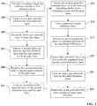
- FIG. 1 is a schematic flowchart of a method for manufacturing a semiconductor device.
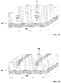
- FIG. 3A to FIG. 3J illustrate schematically perspective views of several phases of the process of manufacturing a semiconductor device according to FIG. 1 . Description is made in the following with reference to FIG. 1 and FIG. 3A to FIG. 3J .
- step 101 a substrate is provided.
- the substrate may include a base layer 300 and a first dielectric layer 302 on the base layer 300.
- the base layer 300 may be made of, for example, a bulk semiconductor such as bulk silicon.
- the material of the first dielectric layer 302 may include an oxide of silicon or a nitride of silicon. It should be understood that the substrate of the present invention may be formed by using methods, process steps, and materials known in this field. Therefore, details of a process of forming the substrate are not described herein.
- step 103 a lower gate material layer on the first dielectric layer is formed.
- the lower gate material layer may include a polysilicon layer 3041 (which may be doped) as shown in FIG. 3A , and optionally, may further include an additional conductive layer 3042 formed on the polysilicon layer 3041.
- the material for the additional conductive layer 3042 may include, for example, doped silicon germanium, a doped silicide of cobalt, or a conductive nitride of boron.
- the polysilicon layer 3041 may be used to enhance adhesion of the conductive layer 3042 to the first dielectric layer 302, or may facilitate formation of the conductive layer 3042.
- step 105 the lower gate material layer is patterned.
- the lower gate material layer may be patterned by using methods and process steps known in this field, such as dry etching or wet etching, so as to form gate lines 304 shown in FIG. 3B .
- the gate line 304 may include a polysilicon layer 3041 and a conductive layer 3042.
- step 107 a second dielectric layer on the first dielectric layer and the gate lines is deposited to cover the gate lines.
- a second dielectric layer 306 is deposited on the first dielectric layer 302 and the gate lines 304 to cover the gate lines 304, as shown in FIG. 3C .
- the material of the second dielectric layer 306 may include an oxide of silicon or a nitride of silicon.
- step 109 the second dielectric layer is planarized to expose upper surfaces of the gate lines.
- the second dielectric layer 306 may be planarized by using a chemical-mechanical planarization (CMP) process, so as to expose upper surfaces of the gate lines 304, as shown in FIG. 3D .
- CMP chemical-mechanical planarization
- step 111 an insulating buffer material layer on the second dielectric layer and the gate lines is formed.
- an insulating buffer material layer 308 may be formed on the second dielectric layer 306 and the gate lines 304 as shown in FIG. 3E , by using process steps such as chemical vapor deposition.
- the material of the insulating buffer material layer 308 may be suitable for selectively growing a graphene layer, and may include, for example, an oxide of aluminum.
- step 113 the insulating buffer material layer is patterned.
- the insulating buffer material layer 308 is patterned, so as to form a patterned insulating buffer layer 308 extending to intersect the gate lines 304, as shown in FIG. 3F .
- the patterned insulating buffer layer 308 may include a plurality of separate portions. Each separate portion corresponds to one or more gate lines 304; and extends to intersect the corresponding gate lines 304.
- the insulating buffer material layer may be patterned by using a nitride of silicon as a hard mask and using a Self-Aligned Double Patterning (Self-Aligned Double Patterning, SADP for short) process, so as to form the patterned insulating buffer layer 308 which extends to intersect the gate lines 304.
- the patterned buffer layer 308 may contain multiple separate portions where each separate portion intersects with one of the gate lines 304. Then, the remaining portions of the hard mask is removed. In this way, a device structure shown in FIG. 3F is obtained.
- step 115 a graphene layer on the insulating buffer layer is selectively grown.
- a graphene layer 310 may be selectively grown (in-situ) on the insulating buffer layer 308, as shown in FIG. 3G , in a temperature environment of 900-1000°C by a chemical vapor deposition process using methane and hydrogen.
- the graphene layer 310 may alternatively be selectively grown (in-situ) on the insulating buffer layer 308 by using other growth techniques, forming the structure as shown in FIG. 3G .
- a third dielectric layer is formed so as to cover the graphene layer and the second dielectric layer.
- a third dielectric layer 312 may be formed by using, for example, a physical vapor deposition process, and then a chemical-mechanical planarization process.
- the third dielectric layer 312 covers the graphene layer 310 and the second dielectric layer 306.
- the material of the third dielectric layer 312 may include, for example: an oxide of silicon, an oxide of hafnium, a nonconductive nitride of boron, or a nitride of aluminum.
- step 119 an upper electrode layer on the third dielectric layer is formed.
- an upper gate electrode layer 314 is formed on the third dielectric layer 312, where the material of the upper gate electrode layer 314 may include materials such as polysilicon, a metal, and/or a silicide of the metal that are suitable for serving as a gate material.
- the method may further include step 121 for patterning the upper gate electrode layer 314 to form one or more upper gate electrodes, such as the dual gates 316 shown in FIG. 3J .
- the method for manufacturing a semiconductor device in this form above provides using a selective growth of graphene to avoid undesired effects associated with patterning graphene by using other processes such as direct laser raster writing and etching or photoetching.
- the semiconductor device according to the present invention may contain a dual-gate structure shown in FIG. 3J and may offer better current control.
- FIG. 2 is a schematic flowchart of another method for manufacturing a semiconductor device.
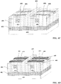
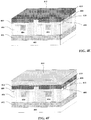
- FIG. 4A to FIG. 4G illustrate schematically perspective views of several phases of a process of manufacturing a semiconductor device according to FIG. 2 . Description is made in the following with reference to FIG. 2 and FIG. 4A to FIG. 4G .
- step 201 to step 211 are same or similar to step 101 to step 111 shown in FIG. 1 . Therefore, step 201 to step 211 are not described herein in detail.
- step 213 an insulating buffer material layer is patterned.
- a first dielectric layer 402 is formed on a base layer 400.
- the base layer 400 may be made of, for example, a bulk semiconductor such as bulk silicon.
- the material of the first dielectric layer 402 may include an oxide of silicon or a nitride of silicon.
- a second dielectric layer 406 covers the first dielectric layer 402, and the top of the second dielectric layer 406is approximately level with the upper surface of the gate lines 404, so that upper surfaces of the gate lines 404 is not covered by the second dielectric layer 406.
- a patterned insulating buffer layer 408 is formed on the gate line 404, and the patterned insulating buffer layer 408 extends to intersect the gate lines 404.
- the patterned insulating buffer layer 408 may include a plurality of separate portions (such as the lines 408 shown in FIG. 4A ). Each separate portion may intersect multiple gate lines 404.
- the material of the patterned insulating buffer layer 408 may be suitable for selectively growing a graphene layer, and includes, for example, an oxide of aluminum.
- step 215 a patterned fourth dielectric layer is formed.
- a fourth dielectric layer 409 may be deposited by using process steps such as chemical vapor deposition, so as to cover the insulating buffer layer 408.
- the material of the fourth dielectric layer 409 may include an oxide of silicon or a nitride of silicon. Following the deposition of the fourth dielectric layer 409 and by using a patterned mask, dry etching is performed to the fourth dielectric layer 409, and residuals are removed by a wet etching process. As a result, a patterned fourth dielectric layer 409 is formed.
- the patterned fourth dielectric layer 409 covers part of the separate portions of the patterned insulating buffer layer 408, and the rest of the patterned insulating buffer layer 408 is exposed and is not covered by the patterned fourth dielectric layer 409.
- the uncovered or exposed part of the patterned insulating buffer layer 408 intersects one or more gate lines 404, as shown in FIG. 4C .
- a graphene layer is selectively grown on the part of the patterned insulating buffer layer uncovered by the patterned fourth insulating layer 409.
- a graphene layer 410 may be selectively grown (in-situ) on the exposed parts of the patterned insulating buffer layer 408 in at a temperature of 900-1000°C by a chemical vapor deposition process using methane and hydrogen.
- the graphene layer 410 may alternatively be selectively grown (in-situ) on the insulating buffer layer 408 using other technical modes.
- step 219 a third dielectric layer is formed.
- a third dielectric layer 412 may be formed by using a physical vapor deposition process, followed by a chemical-mechanical planarization.
- the third dielectric layer 412 covers the graphene layer 410 and the fourth dielectric layer 409.
- the material for the third dielectric layer 412 may include, for example, an oxide of silicon, an oxide of hafnium, a nonconductive nitride of boron, or a nitride of aluminum.
- step 221 an upper gate electrode layer is formed on the third dielectric layer.
- an upper gate electrode layer 414 is formed on the third dielectric layer 412, where the material of the upper gate electrode layer 414 may include materials such as polysilicon, a metal, or a silicide of the metal that are suitable for serving as a gate material.
- the method may further include step 223, in which the upper gate electrode layer 414 is patterned to form an upper gate electrode 416, as shown in FIG. 4G .
- the upper gate electrode layer 414 may be patterned by using methods, process steps, and materials known in this field, so as to form the upper gate electrode 416. Therefore, these methods and processes, and materials are not described herein in detail.
- the method for manufacturing a semiconductor device in the form above may reduce complexity of the process steps of patterning the insulating buffer material layer for selective growth of graphene. Specifically, the separation of portions of the graphene layers may be achieved by covering portions of the insulating buffer layer using the fourth dielectric layer rather than by etching the insulating buffer layer. Furthermore, the selectively grown graphene further help avoid undesired effects associated with patterning graphene using other processes such as direct laser writing or photoetching.
- the semiconductor device according to the present invention includes a dual-gate structure as shown in FIG. 4G that offers better current control.
- this disclosure further teaches a semiconductor device, including: a substrate containing a first dielectric layer; a second dielectric layer and gate lines on the first dielectric layer, where an upper surface of the second dielectric layer flushes with the gate lines.
- the semiconductor device further contains a patterned insulating buffer layer on the second dielectric layer and the gate lines.
- the insulating buffer layer contains multiple separate portions each extending to intersect one or more gate lines.
- the semiconductor device further contains a graphene layer selectively grown on the patterned insulating buffer layer, a third dielectric layer covering the graphene layer and the second dielectric layer, and an upper gate electrode on the third dielectric layer.
- the gate line includes a polysilicon layer and a doped silicon germanium layer on the polysilicon layer.
- the gate line includes a polysilicon layer and a doped layer of silicides of cobalt or a layer of conductive nitrides of boron on the polysilicon layer.
- the material of the insulating buffer layer includes an oxide of aluminum.
- the material of the third dielectric layer includes: an oxide of silicon, an oxide of hafnium, a nonconductive nitride of boron, or a nitride of aluminum.
- This disclosure further teaches another semiconductor device, including: a substrate including a first dielectric layer; a second dielectric layer and gate lines on the first dielectric layer, where an upper surface of the second dielectric layer flushes with the gate lines.
- the semiconductor device further contains a patterned buffer layer on the second dielectric layer and the gate lines where the patterned insulating buffer layer extends to intersect the gate lines.
- the semiconductor device further contains a fourth dielectric layer, part of which covers a portion of the patterned insulating buffer layer and part of which flushes with the rest of the patterned insulating buffer layer, leading to formation of separate portions in the patterned insulating buffer layer (for selective growth of graphene layer of separate portions) where each separated portion intersects one or more gate lines.
- the semiconductor device further contains a graphene layer selectively grown on portions of the patterned insulating buffer layer that are not covered by the fourth dielectric layer, a third dielectric layer covering the graphene layer and the fourth dielectric layer, and an upper gate electrode on the third dielectric layer.
- the gate line above includes a polysilicon layer and a doped silicon germanium layer on the polysilicon layer.
- the gate line above includes a polysilicon layer and a doped layer of silicides of cobalt or a layer of conductive nitrides of boron on the polysilicon layer.
- the material of the insulating buffer layer above includes an oxide of aluminum.
- the material of the third dielectric layer above includes: an oxide of silicon, an oxide of hafnium, a nonconductive nitride of boron, or a nitride of aluminum.
Landscapes
- Thin Film Transistor (AREA)
- Electrodes Of Semiconductors (AREA)
Abstract
Description
- This application is based on and claims priority to Chinese Patent Application
CN201610868166.4 - The present invention relates to the technical field of semiconductor processing, particularly to a semiconductor device and a manufacturing method therefor, and more particularly to a dual-gate graphene semiconductor device and a manufacturing method therefor.
- With the constant development of semiconductor technologies, the size of semiconductor devices have become smaller. Semiconductor devices based on silicon materials are the basis of current semiconductor technologies. Devices based on silicon materials will still be the mainstream of the development of semiconductor technologies at least for an indefinitely long period of time in the future. However, to ensure that semiconductor technologies can continue to evolve according to, for example, the Moore's Law, only reducing the device size proportionally cannot meet the requirements. Therefore, new materials need to be developed in the process of reducing the size of semiconductor devices.
- An ideal new material may be introduced into the existing CMOS manufacturing process, so as to lower chip manufacturing costs while improving device performance. Because graphene materials feature good thermal conductivity and high carrier mobility, graphene-based semiconductor devices are considered by the industry as one of the candidate solutions that offers improvement over silicon-based semiconductor devices in the future.
- Existing methods for patterning graphene mainly include a photolithography method and a direct laser raster writing method. Although the direct laser raster writing method introduces no other reagents in the process of patterning graphene, a patterned features in the graphene layer obtained by using this method may not be fine enough (i.e., may be of insufficient resolution) and may require a long production cycle. The photolithography method, on the other hand, introduces other chemical reagents during etching, and the use of a developing solution and a stripping solution for, e.g., photo resists, will increase the sheet resistance of the patterned graphene.
- Therefore, speedy manufacturing of high-quality semiconductor devices having a patterned graphene layer represents one of the major challenges in the development of new semiconductor processes.
- It is an object of the present invention to provide a method for manufacturing a semiconductor device and a semiconductor device which address at least one of the foregoing problems.
- The object is achieved by the features of the respective independent claims. Further embodiments are defined in the respective dependent claims.
- A first aspect of the present invention provides a first alternative of a method for manufacturing a semiconductor device. The method includes: providing a substrate containing a first dielectric layer; forming a lower gate material layer on the first dielectric layer; patterning the lower gate material layer to form gate lines; depositing a second dielectric layer on the first dielectric layer and the gate lines to cover the gate lines; planarizing the second dielectric layer to expose upper surfaces of the gate lines; forming an insulating buffer material layer on the second dielectric layer and the gate lines. The first alternative of the method further comprises: patterning the insulating buffer material layer to form a patterned insulating buffer layer comprising multiple separate portions, each portion extending to intersect one or more gate lines; selectively growing a graphene layer on the patterned insulating buffer layer; forming a third dielectric layer to cover the graphene layer and the second dielectric layer; and forming an upper gate electrode layer on the third dielectric layer.
- A second aspect of the present invention provides a second alternative of a method for manufacturing a semiconductor device. The method includes: providing a substrate containing a first dielectric layer; forming a lower gate material layer on the first dielectric layer; patterning the lower gate material layer to form gate lines; depositing a second dielectric layer on the first dielectric layer and the gate lines to cover the gate lines; planarizing the second dielectric layer to expose upper surfaces of the gate lines; forming an insulating buffer material layer on the second dielectric layer and the gate lines. The second alternative of the method further comprises: patterning the insulating buffer material layer, so as to form a patterned insulating buffer layer extending to intersect the gate lines; forming a patterned fourth dielectric layer, wherein the patterned fourth dielectric layer covers a portion of the patterned insulating buffer layer and exposes separate portions of the patterned insulating buffer layer, where each exposed portion of the patterned insulating buffer layer intersects one or more gate lines; selectively growing a graphene layer on the exposed portions of the patterned insulating buffer layer; forming a third dielectric layer to cover the graphene layer and the fourth dielectric layer; and forming an upper gate electrode layer on the third dielectric layer.
- The following are detailed embodiments and further developments of the fore-going methods according to the first and second aspect of the present invention.
- Preferably, the lower gate material layer includes a polysilicon layer and a doped silicon germanium layer grown on the polysilicon layer.
- Preferably, the lower gate material layer includes: a polysilicon layer, and a doped layer of silicides of cobalt or a layer of conductive nitrides of boron which is formed on the polysilicon layer.
- Preferably, the graphene layer is selectively grown on the insulating buffer layer at a temperature of 900-1000°C by a chemical vapor deposition process using methane and hydrogen.
- Preferably, the patterned insulating buffer layer includes an oxide of aluminum.
- Preferably, the third dielectric layer includes: an oxide of silicon, an oxide of hafnium, a nonconductive nitride of boron, or a nitride of aluminum.
- Preferably, the methods above further include patterning the upper gate electrode layer to form an upper gate electrode.
- A third aspect of the present invention provides a first alternative of a semiconductor device. The semiconductor device includes: a substrate containing a first dielectric layer; a second dielectric layer and gate lines on the first dielectric layer, wherein an upper surface of the second dielectric layer and an upper surface of the gate lines facing away from the substrate flush with one another; a patterned insulating buffer layer on the second dielectric layer and the gate lines, wherein the patterned insulating buffer layer comprises multiple separate portions each extending to intersect one or more gate lines; a graphene layer selectively grown on the patterned insulating buffer layer; a third dielectric layer covering the graphene layer and the second dielectric layer; and an upper gate electrode on the third dielectric layer.
- A fifth aspect of the present invention provides a second alternative of a semiconductor device. The semiconductor device includes: a substrate containing a first dielectric layer; a second dielectric layer and gate lines on the first dielectric layer, wherein an upper surface of the second dielectric layer and an upper surface of the gate lines facing away from the substrate flush with one another; a patterned insulating buffer layer on the second dielectric layer and the gate lines, wherein the insulating buffer layer extends to intersect the gate lines; a fourth dielectric layer covering part of the patterned insulating buffer layer, and separating the patterned insulating buffer layer into separate portions uncovered by the fourth dielectric layer, wherein each separate uncovered portion of the patterned insulating buffer layer intersects one or more gate lines; a graphene layer selectively grown on the separated portions of the patterned insulating buffer layer; a third dielectric layer covering the graphene layer and the fourth dielectric layer; and an upper gate electrode on the third dielectric layer.
- Preferably, the gate line includes a polysilicon layer and a doped silicon germanium layer on the polysilicon layer.
- Preferably, the gate line includes a polysilicon layer and a doped layer of silicides of cobalt or a layer of conductive nitrides of boron on the polysilicon layer.
- Preferably, the patterned insulating buffer layer includes an oxide of aluminum.
- Preferably, the third dielectric layer includes: an oxide of silicon, an oxide of hafnium, a nonconductive nitride of boron, or a nitride of aluminum.
- A semiconductor device according to the third and fifth, respectively, aspect of the present invention may be obtained by a method according to the first and second, respectively, aspect of the present invention.
- According to the following detailed descriptions of the forms for illustration purposes of the present invention with reference to the accompanying drawings, other characters and advantages of the present invention will become clear.
- The accompanying drawings that form a part of the specification describe forms of the present invention, and are used to explain the principles of the present invention together with the specification.
- With reference to the accompanying drawings, the present invention can be understood more clearly according to the following detailed description, where:
-
FIG. 1 is a schematic flowchart of a method for manufacturing a semiconductor device; -
FIG. 2 is schematic flowchart of another method for manufacturing a semiconductor device; -
FIG. 3A to FIG. 3J illustrate schematically perspective views of several phases of a process of manufacturing a semiconductor device; and -
FIG. 4A to FIG. 4G illustrate schematically perspective views of several phases of another process of manufacturing a semiconductor device. - Various exemplary forms or implementations for illustration purposes of the present invention are described in detail with reference to the accompanying drawings. It should be noted that unless being described in detail, relative layouts, mathematical expressions, and numeric values of components and steps described in these forms do not limit the present invention.
- In addition, it should be noted that for ease of description, sizes of the parts shown in the accompanying drawings are not drawn according to any actual proportional relationship.
- The following description about at least one exemplary form is illustrative only, and would not be used as any limitation on the present invention and applications or uses of the present invention.
- Technologies, methods, and devices that are known by a person of ordinary skill in the related may not be discussed in detail. However, if appropriate, these technologies, methods, and devices should be considered as a part of the description.
- In all examples shown and discussed herein, any specific value should be interpreted to be illustrative only rather than a limitation. Therefore, other examples of the forms for illustration purposes may have different values.
- It should be noted that similar reference numerals, labels, and letters represent similar items in the following accompanying drawings. Therefore, once an item is defined in a figure, the item may be but needs not to be further discussed in subsequent figures.
-
FIG. 1 is a schematic flowchart of a method for manufacturing a semiconductor device.FIG. 3A to FIG. 3J illustrate schematically perspective views of several phases of the process of manufacturing a semiconductor device according toFIG. 1 . Description is made in the following with reference toFIG. 1 andFIG. 3A toFIG. 3J . - As shown in
FIG. 1 , instep 101, a substrate is provided. - As shown in
FIG. 3A , the substrate may include abase layer 300 and a firstdielectric layer 302 on thebase layer 300. Thebase layer 300 may be made of, for example, a bulk semiconductor such as bulk silicon. The material of thefirst dielectric layer 302 may include an oxide of silicon or a nitride of silicon. It should be understood that the substrate of the present invention may be formed by using methods, process steps, and materials known in this field. Therefore, details of a process of forming the substrate are not described herein. - Referring to
FIG. 1 , instep 103, a lower gate material layer on the first dielectric layer is formed. - In an implementation, the lower gate material layer may include a polysilicon layer 3041 (which may be doped) as shown in
FIG. 3A , and optionally, may further include an additionalconductive layer 3042 formed on thepolysilicon layer 3041. The material for the additionalconductive layer 3042 may include, for example, doped silicon germanium, a doped silicide of cobalt, or a conductive nitride of boron. In some of these implementations, thepolysilicon layer 3041 may be used to enhance adhesion of theconductive layer 3042 to thefirst dielectric layer 302, or may facilitate formation of theconductive layer 3042. - Subsequently, as shown in
FIG. 1 , instep 105, the lower gate material layer is patterned. - In an implementation, the lower gate material layer may be patterned by using methods and process steps known in this field, such as dry etching or wet etching, so as to form
gate lines 304 shown inFIG. 3B . In a form as shown inFIG. 3B , thegate line 304 may include apolysilicon layer 3041 and aconductive layer 3042. - Subsequently, as shown in
FIG. 1 , instep 107, a second dielectric layer on the first dielectric layer and the gate lines is deposited to cover the gate lines. - In an implementation, a
second dielectric layer 306 is deposited on thefirst dielectric layer 302 and thegate lines 304 to cover thegate lines 304, as shown inFIG. 3C . The material of thesecond dielectric layer 306 may include an oxide of silicon or a nitride of silicon. - Referring to
FIG. 1 , instep 109 the second dielectric layer is planarized to expose upper surfaces of the gate lines. - In an implementation, for example, the
second dielectric layer 306 may be planarized by using a chemical-mechanical planarization (CMP) process, so as to expose upper surfaces of thegate lines 304, as shown inFIG. 3D . - Subsequently, as shown in
FIG. 1 , instep 111, an insulating buffer material layer on the second dielectric layer and the gate lines is formed. - In an implementation, an insulating
buffer material layer 308 may be formed on thesecond dielectric layer 306 and thegate lines 304 as shown inFIG. 3E , by using process steps such as chemical vapor deposition. The material of the insulatingbuffer material layer 308 may be suitable for selectively growing a graphene layer, and may include, for example, an oxide of aluminum. - Subsequently, as shown in
FIG. 1 , instep 113, the insulating buffer material layer is patterned. - In an implementation, the insulating
buffer material layer 308 is patterned, so as to form a patterned insulatingbuffer layer 308 extending to intersect thegate lines 304, as shown inFIG. 3F . The patterned insulatingbuffer layer 308 may include a plurality of separate portions. Each separate portion corresponds to one ormore gate lines 304; and extends to intersect the corresponding gate lines 304. For example, the insulating buffer material layer may be patterned by using a nitride of silicon as a hard mask and using a Self-Aligned Double Patterning (Self-Aligned Double Patterning, SADP for short) process, so as to form the patterned insulatingbuffer layer 308 which extends to intersect the gate lines 304. In one implementation, the patternedbuffer layer 308 may contain multiple separate portions where each separate portion intersects with one of the gate lines 304. Then, the remaining portions of the hard mask is removed. In this way, a device structure shown inFIG. 3F is obtained. - Referring to
FIG. 1 , instep 115, a graphene layer on the insulating buffer layer is selectively grown. - In an implementation, a
graphene layer 310 may be selectively grown (in-situ) on the insulatingbuffer layer 308, as shown inFIG. 3G , in a temperature environment of 900-1000°C by a chemical vapor deposition process using methane and hydrogen. Thegraphene layer 310 may alternatively be selectively grown (in-situ) on the insulatingbuffer layer 308 by using other growth techniques, forming the structure as shown inFIG. 3G . - Subsequently, as shown in
FIG. 1 , instep 117, a third dielectric layer is formed so as to cover the graphene layer and the second dielectric layer. - In an implementation, as shown in
FIG. 3H , a thirddielectric layer 312 may be formed by using, for example, a physical vapor deposition process, and then a chemical-mechanical planarization process. The thirddielectric layer 312 covers thegraphene layer 310 and thesecond dielectric layer 306. The material of the thirddielectric layer 312 may include, for example: an oxide of silicon, an oxide of hafnium, a nonconductive nitride of boron, or a nitride of aluminum. - Subsequently, as shown in
FIG. 1 , instep 119, an upper electrode layer on the third dielectric layer is formed. - In an implementation, as shown in
FIG. 3I , an uppergate electrode layer 314 is formed on the thirddielectric layer 312, where the material of the uppergate electrode layer 314 may include materials such as polysilicon, a metal, and/or a silicide of the metal that are suitable for serving as a gate material. - Optionally, as shown in
FIG. 1 , afterstep 119, the method may further includestep 121 for patterning the uppergate electrode layer 314 to form one or more upper gate electrodes, such as thedual gates 316 shown inFIG. 3J . - The method for manufacturing a semiconductor device in this form above provides using a selective growth of graphene to avoid undesired effects associated with patterning graphene by using other processes such as direct laser raster writing and etching or photoetching. In addition, the semiconductor device according to the present invention may contain a dual-gate structure shown in
FIG. 3J and may offer better current control. -
FIG. 2 is a schematic flowchart of another method for manufacturing a semiconductor device.FIG. 4A to FIG. 4G illustrate schematically perspective views of several phases of a process of manufacturing a semiconductor device according toFIG. 2 . Description is made in the following with reference toFIG. 2 andFIG. 4A toFIG. 4G . - As shown in
FIG. 2 , step 201 to step 211 are same or similar to step 101 to step 111 shown inFIG. 1 . Therefore, step 201 to step 211 are not described herein in detail. - In
step 213, an insulating buffer material layer is patterned. - One implementation is shown in
FIG. 4A by a perspective view of a device obtained after steps 201-213. Afirst dielectric layer 402 is formed on abase layer 400. Thebase layer 400 may be made of, for example, a bulk semiconductor such as bulk silicon. The material of thefirst dielectric layer 402 may include an oxide of silicon or a nitride of silicon. Asecond dielectric layer 406 covers thefirst dielectric layer 402, and the top of the second dielectric layer 406is approximately level with the upper surface of thegate lines 404, so that upper surfaces of the gate lines 404 is not covered by thesecond dielectric layer 406. A patterned insulatingbuffer layer 408 is formed on thegate line 404, and the patterned insulatingbuffer layer 408 extends to intersect the gate lines 404. The patterned insulatingbuffer layer 408 may include a plurality of separate portions (such as thelines 408 shown inFIG. 4A ). Each separate portion may intersect multiple gate lines 404. The material of the patterned insulatingbuffer layer 408 may be suitable for selectively growing a graphene layer, and includes, for example, an oxide of aluminum. - Referring to
FIG. 2 , instep 215, a patterned fourth dielectric layer is formed. - In an implementation, as shown in
Fig. 4B , a fourthdielectric layer 409 may be deposited by using process steps such as chemical vapor deposition, so as to cover the insulatingbuffer layer 408. The material of thefourth dielectric layer 409 may include an oxide of silicon or a nitride of silicon. Following the deposition of thefourth dielectric layer 409 and by using a patterned mask, dry etching is performed to thefourth dielectric layer 409, and residuals are removed by a wet etching process. As a result, a patterned fourthdielectric layer 409 is formed. The patterned fourthdielectric layer 409 covers part of the separate portions of the patterned insulatingbuffer layer 408, and the rest of the patterned insulatingbuffer layer 408 is exposed and is not covered by the patterned fourthdielectric layer 409. The uncovered or exposed part of the patterned insulatingbuffer layer 408 intersects one ormore gate lines 404, as shown inFIG. 4C . - Subsequently, as shown in
FIG. 2 , instep 217, a graphene layer is selectively grown on the part of the patterned insulating buffer layer uncovered by the patterned fourth insulatinglayer 409. - In an implementation, as shown in
FIG. 4D , agraphene layer 410 may be selectively grown (in-situ) on the exposed parts of the patterned insulatingbuffer layer 408 in at a temperature of 900-1000°C by a chemical vapor deposition process using methane and hydrogen. Thegraphene layer 410 may alternatively be selectively grown (in-situ) on the insulatingbuffer layer 408 using other technical modes. - Subsequently, referring to
FIG. 2 , instep 219, a third dielectric layer is formed. - In an implementation, as shown in
FIG. 4E , a thirddielectric layer 412 may be formed by using a physical vapor deposition process, followed by a chemical-mechanical planarization. The thirddielectric layer 412 covers thegraphene layer 410 and thefourth dielectric layer 409. The material for the thirddielectric layer 412 may include, for example, an oxide of silicon, an oxide of hafnium, a nonconductive nitride of boron, or a nitride of aluminum. - Subsequently, as shown in
FIG. 2 , instep 221, an upper gate electrode layer is formed on the third dielectric layer. - In an implementation, as shown in
FIG. 4F , an uppergate electrode layer 414 is formed on the thirddielectric layer 412, where the material of the uppergate electrode layer 414 may include materials such as polysilicon, a metal, or a silicide of the metal that are suitable for serving as a gate material. - Optionally, as shown in
FIG. 2 , afterstep 221, the method may further includestep 223, in which the uppergate electrode layer 414 is patterned to form anupper gate electrode 416, as shown inFIG. 4G . It should be understood that the uppergate electrode layer 414 may be patterned by using methods, process steps, and materials known in this field, so as to form theupper gate electrode 416. Therefore, these methods and processes, and materials are not described herein in detail. - The method for manufacturing a semiconductor device in the form above (
FIGs. 2 and4 ) may reduce complexity of the process steps of patterning the insulating buffer material layer for selective growth of graphene. Specifically, the separation of portions of the graphene layers may be achieved by covering portions of the insulating buffer layer using the fourth dielectric layer rather than by etching the insulating buffer layer. Furthermore, the selectively grown graphene further help avoid undesired effects associated with patterning graphene using other processes such as direct laser writing or photoetching. In addition, the semiconductor device according to the present invention includes a dual-gate structure as shown inFIG. 4G that offers better current control. - It should be understood that this disclosure further teaches a semiconductor device, including: a substrate containing a first dielectric layer; a second dielectric layer and gate lines on the first dielectric layer, where an upper surface of the second dielectric layer flushes with the gate lines. The semiconductor device further contains a patterned insulating buffer layer on the second dielectric layer and the gate lines. The insulating buffer layer contains multiple separate portions each extending to intersect one or more gate lines. The semiconductor device further contains a graphene layer selectively grown on the patterned insulating buffer layer, a third dielectric layer covering the graphene layer and the second dielectric layer, and an upper gate electrode on the third dielectric layer.
- In an implementation, the gate line includes a polysilicon layer and a doped silicon germanium layer on the polysilicon layer.
- In an implementation, the gate line includes a polysilicon layer and a doped layer of silicides of cobalt or a layer of conductive nitrides of boron on the polysilicon layer.
- In an implementation, the material of the insulating buffer layer includes an oxide of aluminum.
- In an implementation, the material of the third dielectric layer includes: an oxide of silicon, an oxide of hafnium, a nonconductive nitride of boron, or a nitride of aluminum.
- This disclosure further teaches another semiconductor device, including: a substrate including a first dielectric layer; a second dielectric layer and gate lines on the first dielectric layer, where an upper surface of the second dielectric layer flushes with the gate lines. The semiconductor device further contains a patterned buffer layer on the second dielectric layer and the gate lines where the patterned insulating buffer layer extends to intersect the gate lines. The semiconductor device further contains a fourth dielectric layer, part of which covers a portion of the patterned insulating buffer layer and part of which flushes with the rest of the patterned insulating buffer layer, leading to formation of separate portions in the patterned insulating buffer layer (for selective growth of graphene layer of separate portions) where each separated portion intersects one or more gate lines. The semiconductor device further contains a graphene layer selectively grown on portions of the patterned insulating buffer layer that are not covered by the fourth dielectric layer, a third dielectric layer covering the graphene layer and the fourth dielectric layer, and an upper gate electrode on the third dielectric layer.
- In an implementation, the gate line above includes a polysilicon layer and a doped silicon germanium layer on the polysilicon layer.
- In an alternative implementation, the gate line above includes a polysilicon layer and a doped layer of silicides of cobalt or a layer of conductive nitrides of boron on the polysilicon layer.
- In an implementation, the material of the insulating buffer layer above includes an oxide of aluminum.
- In an implementation, the material of the third dielectric layer above includes: an oxide of silicon, an oxide of hafnium, a nonconductive nitride of boron, or a nitride of aluminum.
Claims (14)
- A method for manufacturing a semiconductor device, comprising:providing a substrate comprising a first dielectric layer;forming a lower gate material layer on the first dielectric layer;patterning the lower gate material layer to form gate lines;depositing a second dielectric layer on the first dielectric layer and the gate lines to cover the gate lines;planarizing the second dielectric layer to expose upper surfaces of the gate lines;forming an insulating buffer material layer on the second dielectric layer and the gate lines;patterning the insulating buffer material layer to form a patterned insulating buffer layer comprising multiple separate portions, each portion extending to intersect one or more gate lines;selectively growing a graphene layer on the patterned insulating buffer layer;forming a third dielectric layer to cover the graphene layer and the second dielectric layer; andforming an upper gate electrode layer on the third dielectric layer.
- The method according to claim 1, wherein the insulating buffer material layer comprises an oxide of aluminum.
- The method according to claim 1 or 2, wherein the third dielectric layer comprises an oxide of silicon, an oxide of hafnium, a nonconductive nitride of boron, or a nitride of aluminum.
- A method for manufacturing a semiconductor device, comprising:providing a substrate comprising a first dielectric layer;forming a lower gate material layer on the first dielectric layer;patterning the lower gate material layer to form gate lines;depositing a second dielectric layer on the first dielectric layer and the gate lines to cover the gate lines;planarizing the second dielectric layer to expose upper surfaces of the gate lines;forming an insulating buffer material layer on the second dielectric layer and the gate lines;patterning the insulating buffer material layer to form a patterned insulating buffer layer extending to intersect the gate lines;forming a patterned fourth dielectric layer, wherein the patterned fourth dielectric layer covers a portion of the patterned insulating buffer layer and exposes separate portions of the patterned insulating buffer layer, where each exposed portion of the patterned insulating buffer layer intersects one or more gate lines;selectively growing a graphene layer on the exposed portions of the patterned insulating buffer layer;forming a third dielectric layer to cover the graphene layer and the fourth dielectric layer; andforming an upper gate electrode layer on the third dielectric layer.
- The method according to claim 4, wherein the insulating buffer material layer comprises an oxide of aluminum and the third dielectric layer comprises an oxide of silicon, an oxide of hafnium, a nonconductive nitride of boron, or a nitride of aluminum.
- The method according to anyone of the claims 1-5, wherein the lower gate material layer comprises a polysilicon layer and a doped silicon germanium layer grown on the polysilicon layer, or a polysilicon layer, and a doped layer of silicides of cobalt or a layer of conductive nitrides of boron formed on the polysilicon layer.
- The method according to anyone of the claims 1-6, wherein the graphene layer is selectively grown on the patterned insulating buffer layer at a temperature of 900-1000°C by a chemical vapor deposition process using methane and hydrogen.
- The method according to anyone of the claims 1-7, further comprising patterning the upper gate electrode layer to form an upper gate electrode.
- A semiconductor device, comprising:a substrate comprising a first dielectric layer;a second dielectric layer and gate lines on the first dielectric layer, wherein an upper surface of the second dielectric layer and an upper surface of the gate lines facing away from the substrate are flush with one another;a patterned insulating buffer layer on the second dielectric layer and the gate lines, wherein the patterned insulating buffer layer comprises multiple separate portions each extending to intersect one or more gate lines;a graphene layer selectively grown on the patterned insulating buffer layer;a third dielectric layer covering the graphene layer and the second dielectric layer; andan upper gate electrode on the third dielectric layer.
- A semiconductor device, comprising:a substrate comprising a first dielectric layer;a second dielectric layer and gate lines on the first dielectric layer, wherein an upper surface of the second dielectric layer and an upper surface of the gate lines facing away from the substrate flush with one another;a patterned insulating buffer layer on the second dielectric layer and the gate lines, wherein the insulating buffer layer extends to intersect the gate lines;a fourth dielectric layer covering part of the patterned insulating buffer layer, and separating the patterned insulating buffer layer into separate portions uncovered by the fourth dielectric layer, wherein each separate uncovered portion of the patterned insulating buffer layer intersects one or more gate lines;a graphene layer selectively grown on the separated portions of the patterned insulating buffer layer;a third dielectric layer covering the graphene layer and the fourth dielectric layer; andan upper gate electrode on the third dielectric layer.
- The device according to claim 9 or 10, wherein the gate line comprises a polysilicon layer and a doped silicon germanium layer on the polysilicon layer.
- The device according to anyone of the claims 9-11, wherein the gate line comprises a polysilicon layer and a doped layer of silicides of cobalt or a layer of conductive nitrides of boron on the polysilicon layer.
- The device according to anyone of the claims 9-12, wherein the patterned insulating buffer layer comprises an oxide of aluminum.
- The device according to anyone of the claims 9-13, wherein the third dielectric layer comprises an oxide of silicon, an oxide of hafnium, a nonconductive nitride of boron, or a nitride of aluminum.
Applications Claiming Priority (1)
| Application Number | Priority Date | Filing Date | Title |
|---|---|---|---|
| CN201610868166.4A CN107887333B (en) | 2016-09-30 | 2016-09-30 | Semiconductor device and method of manufacturing the same |
Publications (2)
| Publication Number | Publication Date |
|---|---|
| EP3301723A1 true EP3301723A1 (en) | 2018-04-04 |
| EP3301723B1 EP3301723B1 (en) | 2020-11-04 |
Family
ID=59799231
Family Applications (1)
| Application Number | Title | Priority Date | Filing Date |
|---|---|---|---|
| EP17188981.9A Not-in-force EP3301723B1 (en) | 2016-09-30 | 2017-09-01 | Semiconductor device and manufacturing method therefor |
Country Status (3)
| Country | Link |
|---|---|
| US (1) | US10121872B2 (en) |
| EP (1) | EP3301723B1 (en) |
| CN (1) | CN107887333B (en) |
Citations (2)
| Publication number | Priority date | Publication date | Assignee | Title |
|---|---|---|---|---|
| US20100200839A1 (en) * | 2008-11-26 | 2010-08-12 | Makoto Okai | Graphene grown substrate and electronic/photonic integrated circuits using same |
| US20120175594A1 (en) * | 2011-01-07 | 2012-07-12 | International Business Machines Corporation | Graphene Devices with Local Dual Gates |
Family Cites Families (6)
| Publication number | Priority date | Publication date | Assignee | Title |
|---|---|---|---|---|
| KR100553682B1 (en) * | 2003-03-07 | 2006-02-24 | 삼성전자주식회사 | A semiconductor device having a gate electrode and a method of forming the same |
| CN101442105B (en) * | 2007-11-21 | 2010-06-09 | 中国科学院化学研究所 | An organic field effect transistor, its special source and drain electrodes and its preparation method |
| WO2011058651A1 (en) * | 2009-11-13 | 2011-05-19 | 富士通株式会社 | Semiconductor device and process for manufacturing same |
| WO2012170099A2 (en) * | 2011-03-22 | 2012-12-13 | Massachusetts Institute Of Technology | Direct synthesis of patterned graphene by deposition |
| CN105374757B (en) * | 2015-10-19 | 2019-05-21 | 中国科学院微电子研究所 | Semiconductor device and method of manufacturing the same |
| US10236347B2 (en) * | 2016-08-08 | 2019-03-19 | King Abdullah University Of Science And Technology | Method of producing an electronic device with a graphene device and semiconductor device formed on a common semiconductor substrate |
-
2016
- 2016-09-30 CN CN201610868166.4A patent/CN107887333B/en active Active
-
2017
- 2017-08-22 US US15/683,106 patent/US10121872B2/en active Active
- 2017-09-01 EP EP17188981.9A patent/EP3301723B1/en not_active Not-in-force
Patent Citations (2)
| Publication number | Priority date | Publication date | Assignee | Title |
|---|---|---|---|---|
| US20100200839A1 (en) * | 2008-11-26 | 2010-08-12 | Makoto Okai | Graphene grown substrate and electronic/photonic integrated circuits using same |
| US20120175594A1 (en) * | 2011-01-07 | 2012-07-12 | International Business Machines Corporation | Graphene Devices with Local Dual Gates |
Also Published As
| Publication number | Publication date |
|---|---|
| CN107887333B (en) | 2020-07-31 |
| US10121872B2 (en) | 2018-11-06 |
| CN107887333A (en) | 2018-04-06 |
| EP3301723B1 (en) | 2020-11-04 |
| US20180097082A1 (en) | 2018-04-05 |
Similar Documents
| Publication | Publication Date | Title |
|---|---|---|
| US10170623B2 (en) | Method of fabricating semiconductor device | |
| US9478622B2 (en) | Wrap-around contact for finFET | |
| US9431514B2 (en) | FinFET device having a high germanium content fin structure and method of making same | |
| US9466521B2 (en) | Semiconductor device having a patterned metal layer embedded in an interlayer dielectric layer | |
| US9224617B2 (en) | Forming cross-coupled line segments | |
| US8962408B2 (en) | Replacement gate self-aligned carbon nanostructure transistor | |
| EP3301722B1 (en) | Semiconductor device and manufacturing method therefor | |
| CN109119340A (en) | The stack strip nanometer shape and its structure being made of different semiconductor materials | |
| CN102214576A (en) | Semiconductor device and manufacturing method thereof | |
| CN108695382B (en) | Semiconductor device and method of manufacturing the same | |
| TW201801194A (en) | Method for fabricating source-drain contacts for fin field effect transistors | |
| US9048216B2 (en) | Self aligned embedded gate carbon transistors | |
| US9224654B2 (en) | Fin capacitor employing sidewall image transfer | |
| CN102237311B (en) | Semiconductor device and manufacturing method thereof | |
| US20140145267A1 (en) | Semiconductor device and method of fabricating same | |
| EP3301723B1 (en) | Semiconductor device and manufacturing method therefor | |
| CN108695233B (en) | Semiconductor device and method of manufacturing the same | |
| US10134849B2 (en) | Semiconductor device and manufacturing method thereof | |
| US11955483B2 (en) | Semiconductor device and fabrication method thereof | |
| CN109494249B (en) | Semiconductor device and method for manufacturing the same | |
| CN103972087A (en) | Semiconductor device manufacturing method |
Legal Events
| Date | Code | Title | Description |
|---|---|---|---|
| PUAI | Public reference made under article 153(3) epc to a published international application that has entered the european phase |
Free format text: ORIGINAL CODE: 0009012 |
|
| STAA | Information on the status of an ep patent application or granted ep patent |
Free format text: STATUS: THE APPLICATION HAS BEEN PUBLISHED |
|
| AK | Designated contracting states |
Kind code of ref document: A1 Designated state(s): AL AT BE BG CH CY CZ DE DK EE ES FI FR GB GR HR HU IE IS IT LI LT LU LV MC MK MT NL NO PL PT RO RS SE SI SK SM TR |
|
| AX | Request for extension of the european patent |
Extension state: BA ME |
|
| STAA | Information on the status of an ep patent application or granted ep patent |
Free format text: STATUS: REQUEST FOR EXAMINATION WAS MADE |
|
| 17P | Request for examination filed |
Effective date: 20180809 |
|
| RBV | Designated contracting states (corrected) |
Designated state(s): AL AT BE BG CH CY CZ DE DK EE ES FI FR GB GR HR HU IE IS IT LI LT LU LV MC MK MT NL NO PL PT RO RS SE SI SK SM TR |
|
| RAP1 | Party data changed (applicant data changed or rights of an application transferred) |
Owner name: SEMICONDUCTOR MANUFACTURING INTERNATIONAL (BEIJING Owner name: SEMICONDUCTOR MANUFACTURING INTERNATIONAL (SHANGHA |
|
| GRAP | Despatch of communication of intention to grant a patent |
Free format text: ORIGINAL CODE: EPIDOSNIGR1 |
|
| STAA | Information on the status of an ep patent application or granted ep patent |
Free format text: STATUS: GRANT OF PATENT IS INTENDED |
|
| INTG | Intention to grant announced |
Effective date: 20200423 |
|
| GRAS | Grant fee paid |
Free format text: ORIGINAL CODE: EPIDOSNIGR3 |
|
| GRAA | (expected) grant |
Free format text: ORIGINAL CODE: 0009210 |
|
| STAA | Information on the status of an ep patent application or granted ep patent |
Free format text: STATUS: THE PATENT HAS BEEN GRANTED |
|
| AK | Designated contracting states |
Kind code of ref document: B1 Designated state(s): AL AT BE BG CH CY CZ DE DK EE ES FI FR GB GR HR HU IE IS IT LI LT LU LV MC MK MT NL NO PL PT RO RS SE SI SK SM TR |
|
| REG | Reference to a national code |
Ref country code: GB Ref legal event code: FG4D |
|
| REG | Reference to a national code |
Ref country code: CH Ref legal event code: EP |
|
| REG | Reference to a national code |
Ref country code: AT Ref legal event code: REF Ref document number: 1331939 Country of ref document: AT Kind code of ref document: T Effective date: 20201115 |
|
| REG | Reference to a national code |
Ref country code: IE Ref legal event code: FG4D |
|
| REG | Reference to a national code |
Ref country code: DE Ref legal event code: R096 Ref document number: 602017026679 Country of ref document: DE |
|
| REG | Reference to a national code |
Ref country code: NL Ref legal event code: MP Effective date: 20201104 |
|
| REG | Reference to a national code |
Ref country code: AT Ref legal event code: MK05 Ref document number: 1331939 Country of ref document: AT Kind code of ref document: T Effective date: 20201104 |
|
| PG25 | Lapsed in a contracting state [announced via postgrant information from national office to epo] |
Ref country code: NO Free format text: LAPSE BECAUSE OF FAILURE TO SUBMIT A TRANSLATION OF THE DESCRIPTION OR TO PAY THE FEE WITHIN THE PRESCRIBED TIME-LIMIT Effective date: 20210204 Ref country code: PT Free format text: LAPSE BECAUSE OF FAILURE TO SUBMIT A TRANSLATION OF THE DESCRIPTION OR TO PAY THE FEE WITHIN THE PRESCRIBED TIME-LIMIT Effective date: 20210304 Ref country code: RS Free format text: LAPSE BECAUSE OF FAILURE TO SUBMIT A TRANSLATION OF THE DESCRIPTION OR TO PAY THE FEE WITHIN THE PRESCRIBED TIME-LIMIT Effective date: 20201104 Ref country code: GR Free format text: LAPSE BECAUSE OF FAILURE TO SUBMIT A TRANSLATION OF THE DESCRIPTION OR TO PAY THE FEE WITHIN THE PRESCRIBED TIME-LIMIT Effective date: 20210205 Ref country code: FI Free format text: LAPSE BECAUSE OF FAILURE TO SUBMIT A TRANSLATION OF THE DESCRIPTION OR TO PAY THE FEE WITHIN THE PRESCRIBED TIME-LIMIT Effective date: 20201104 |
|
| PG25 | Lapsed in a contracting state [announced via postgrant information from national office to epo] |
Ref country code: SE Free format text: LAPSE BECAUSE OF FAILURE TO SUBMIT A TRANSLATION OF THE DESCRIPTION OR TO PAY THE FEE WITHIN THE PRESCRIBED TIME-LIMIT Effective date: 20201104 Ref country code: BG Free format text: LAPSE BECAUSE OF FAILURE TO SUBMIT A TRANSLATION OF THE DESCRIPTION OR TO PAY THE FEE WITHIN THE PRESCRIBED TIME-LIMIT Effective date: 20210204 Ref country code: LV Free format text: LAPSE BECAUSE OF FAILURE TO SUBMIT A TRANSLATION OF THE DESCRIPTION OR TO PAY THE FEE WITHIN THE PRESCRIBED TIME-LIMIT Effective date: 20201104 Ref country code: IS Free format text: LAPSE BECAUSE OF FAILURE TO SUBMIT A TRANSLATION OF THE DESCRIPTION OR TO PAY THE FEE WITHIN THE PRESCRIBED TIME-LIMIT Effective date: 20210304 Ref country code: PL Free format text: LAPSE BECAUSE OF FAILURE TO SUBMIT A TRANSLATION OF THE DESCRIPTION OR TO PAY THE FEE WITHIN THE PRESCRIBED TIME-LIMIT Effective date: 20201104 Ref country code: AT Free format text: LAPSE BECAUSE OF FAILURE TO SUBMIT A TRANSLATION OF THE DESCRIPTION OR TO PAY THE FEE WITHIN THE PRESCRIBED TIME-LIMIT Effective date: 20201104 Ref country code: ES Free format text: LAPSE BECAUSE OF FAILURE TO SUBMIT A TRANSLATION OF THE DESCRIPTION OR TO PAY THE FEE WITHIN THE PRESCRIBED TIME-LIMIT Effective date: 20201104 |
|
| REG | Reference to a national code |
Ref country code: LT Ref legal event code: MG9D |
|
| PG25 | Lapsed in a contracting state [announced via postgrant information from national office to epo] |
Ref country code: HR Free format text: LAPSE BECAUSE OF FAILURE TO SUBMIT A TRANSLATION OF THE DESCRIPTION OR TO PAY THE FEE WITHIN THE PRESCRIBED TIME-LIMIT Effective date: 20201104 |
|
| PG25 | Lapsed in a contracting state [announced via postgrant information from national office to epo] |
Ref country code: RO Free format text: LAPSE BECAUSE OF FAILURE TO SUBMIT A TRANSLATION OF THE DESCRIPTION OR TO PAY THE FEE WITHIN THE PRESCRIBED TIME-LIMIT Effective date: 20201104 Ref country code: SK Free format text: LAPSE BECAUSE OF FAILURE TO SUBMIT A TRANSLATION OF THE DESCRIPTION OR TO PAY THE FEE WITHIN THE PRESCRIBED TIME-LIMIT Effective date: 20201104 Ref country code: EE Free format text: LAPSE BECAUSE OF FAILURE TO SUBMIT A TRANSLATION OF THE DESCRIPTION OR TO PAY THE FEE WITHIN THE PRESCRIBED TIME-LIMIT Effective date: 20201104 Ref country code: CZ Free format text: LAPSE BECAUSE OF FAILURE TO SUBMIT A TRANSLATION OF THE DESCRIPTION OR TO PAY THE FEE WITHIN THE PRESCRIBED TIME-LIMIT Effective date: 20201104 Ref country code: SM Free format text: LAPSE BECAUSE OF FAILURE TO SUBMIT A TRANSLATION OF THE DESCRIPTION OR TO PAY THE FEE WITHIN THE PRESCRIBED TIME-LIMIT Effective date: 20201104 Ref country code: LT Free format text: LAPSE BECAUSE OF FAILURE TO SUBMIT A TRANSLATION OF THE DESCRIPTION OR TO PAY THE FEE WITHIN THE PRESCRIBED TIME-LIMIT Effective date: 20201104 |
|
| REG | Reference to a national code |
Ref country code: DE Ref legal event code: R097 Ref document number: 602017026679 Country of ref document: DE |
|
| PG25 | Lapsed in a contracting state [announced via postgrant information from national office to epo] |
Ref country code: DK Free format text: LAPSE BECAUSE OF FAILURE TO SUBMIT A TRANSLATION OF THE DESCRIPTION OR TO PAY THE FEE WITHIN THE PRESCRIBED TIME-LIMIT Effective date: 20201104 |
|
| PLBE | No opposition filed within time limit |
Free format text: ORIGINAL CODE: 0009261 |
|
| STAA | Information on the status of an ep patent application or granted ep patent |
Free format text: STATUS: NO OPPOSITION FILED WITHIN TIME LIMIT |
|
| 26N | No opposition filed |
Effective date: 20210805 |
|
| PG25 | Lapsed in a contracting state [announced via postgrant information from national office to epo] |
Ref country code: IT Free format text: LAPSE BECAUSE OF FAILURE TO SUBMIT A TRANSLATION OF THE DESCRIPTION OR TO PAY THE FEE WITHIN THE PRESCRIBED TIME-LIMIT Effective date: 20201104 Ref country code: NL Free format text: LAPSE BECAUSE OF FAILURE TO SUBMIT A TRANSLATION OF THE DESCRIPTION OR TO PAY THE FEE WITHIN THE PRESCRIBED TIME-LIMIT Effective date: 20201104 Ref country code: AL Free format text: LAPSE BECAUSE OF FAILURE TO SUBMIT A TRANSLATION OF THE DESCRIPTION OR TO PAY THE FEE WITHIN THE PRESCRIBED TIME-LIMIT Effective date: 20201104 |
|
| PG25 | Lapsed in a contracting state [announced via postgrant information from national office to epo] |
Ref country code: SI Free format text: LAPSE BECAUSE OF FAILURE TO SUBMIT A TRANSLATION OF THE DESCRIPTION OR TO PAY THE FEE WITHIN THE PRESCRIBED TIME-LIMIT Effective date: 20201104 |
|
| REG | Reference to a national code |
Ref country code: DE Ref legal event code: R119 Ref document number: 602017026679 Country of ref document: DE |
|
| REG | Reference to a national code |
Ref country code: CH Ref legal event code: PL |
|
| REG | Reference to a national code |
Ref country code: BE Ref legal event code: MM Effective date: 20210930 |
|
| GBPC | Gb: european patent ceased through non-payment of renewal fee |
Effective date: 20210901 |
|
| PG25 | Lapsed in a contracting state [announced via postgrant information from national office to epo] |
Ref country code: IS Free format text: LAPSE BECAUSE OF FAILURE TO SUBMIT A TRANSLATION OF THE DESCRIPTION OR TO PAY THE FEE WITHIN THE PRESCRIBED TIME-LIMIT Effective date: 20210304 Ref country code: MC Free format text: LAPSE BECAUSE OF FAILURE TO SUBMIT A TRANSLATION OF THE DESCRIPTION OR TO PAY THE FEE WITHIN THE PRESCRIBED TIME-LIMIT Effective date: 20201104 |
|
| PG25 | Lapsed in a contracting state [announced via postgrant information from national office to epo] |
Ref country code: LU Free format text: LAPSE BECAUSE OF NON-PAYMENT OF DUE FEES Effective date: 20210901 Ref country code: IE Free format text: LAPSE BECAUSE OF NON-PAYMENT OF DUE FEES Effective date: 20210901 Ref country code: GB Free format text: LAPSE BECAUSE OF NON-PAYMENT OF DUE FEES Effective date: 20210901 Ref country code: FR Free format text: LAPSE BECAUSE OF NON-PAYMENT OF DUE FEES Effective date: 20210930 Ref country code: DE Free format text: LAPSE BECAUSE OF NON-PAYMENT OF DUE FEES Effective date: 20220401 Ref country code: BE Free format text: LAPSE BECAUSE OF NON-PAYMENT OF DUE FEES Effective date: 20210930 |
|
| PG25 | Lapsed in a contracting state [announced via postgrant information from national office to epo] |
Ref country code: LI Free format text: LAPSE BECAUSE OF NON-PAYMENT OF DUE FEES Effective date: 20210930 Ref country code: CH Free format text: LAPSE BECAUSE OF NON-PAYMENT OF DUE FEES Effective date: 20210930 |
|
| PG25 | Lapsed in a contracting state [announced via postgrant information from national office to epo] |
Ref country code: HU Free format text: LAPSE BECAUSE OF FAILURE TO SUBMIT A TRANSLATION OF THE DESCRIPTION OR TO PAY THE FEE WITHIN THE PRESCRIBED TIME-LIMIT; INVALID AB INITIO Effective date: 20170901 |
|
| PG25 | Lapsed in a contracting state [announced via postgrant information from national office to epo] |
Ref country code: CY Free format text: LAPSE BECAUSE OF FAILURE TO SUBMIT A TRANSLATION OF THE DESCRIPTION OR TO PAY THE FEE WITHIN THE PRESCRIBED TIME-LIMIT Effective date: 20201104 |
|
| PG25 | Lapsed in a contracting state [announced via postgrant information from national office to epo] |
Ref country code: MK Free format text: LAPSE BECAUSE OF FAILURE TO SUBMIT A TRANSLATION OF THE DESCRIPTION OR TO PAY THE FEE WITHIN THE PRESCRIBED TIME-LIMIT Effective date: 20201104 |
|
| PG25 | Lapsed in a contracting state [announced via postgrant information from national office to epo] |
Ref country code: MT Free format text: LAPSE BECAUSE OF FAILURE TO SUBMIT A TRANSLATION OF THE DESCRIPTION OR TO PAY THE FEE WITHIN THE PRESCRIBED TIME-LIMIT Effective date: 20201104 |
|
| PG25 | Lapsed in a contracting state [announced via postgrant information from national office to epo] |
Ref country code: TR Free format text: LAPSE BECAUSE OF FAILURE TO SUBMIT A TRANSLATION OF THE DESCRIPTION OR TO PAY THE FEE WITHIN THE PRESCRIBED TIME-LIMIT Effective date: 20201104 |