EP3301722A1 - Semiconductor device and manufacturing method therefor - Google Patents
Semiconductor device and manufacturing method therefor Download PDFInfo
- Publication number
- EP3301722A1 EP3301722A1 EP17188978.5A EP17188978A EP3301722A1 EP 3301722 A1 EP3301722 A1 EP 3301722A1 EP 17188978 A EP17188978 A EP 17188978A EP 3301722 A1 EP3301722 A1 EP 3301722A1
- Authority
- EP
- European Patent Office
- Prior art keywords
- layer
- dielectric layer
- nanowire
- graphene
- material layer
- Prior art date
- Legal status (The legal status is an assumption and is not a legal conclusion. Google has not performed a legal analysis and makes no representation as to the accuracy of the status listed.)
- Granted
Links
Images








Classifications
-
- H—ELECTRICITY
- H10—SEMICONDUCTOR DEVICES; ELECTRIC SOLID-STATE DEVICES NOT OTHERWISE PROVIDED FOR
- H10D—INORGANIC ELECTRIC SEMICONDUCTOR DEVICES
- H10D62/00—Semiconductor bodies, or regions thereof, of devices having potential barriers
- H10D62/80—Semiconductor bodies, or regions thereof, of devices having potential barriers characterised by the materials
- H10D62/83—Semiconductor bodies, or regions thereof, of devices having potential barriers characterised by the materials being Group IV materials, e.g. B-doped Si or undoped Ge
- H10D62/8303—Diamond
-
- H—ELECTRICITY
- H10—SEMICONDUCTOR DEVICES; ELECTRIC SOLID-STATE DEVICES NOT OTHERWISE PROVIDED FOR
- H10D—INORGANIC ELECTRIC SEMICONDUCTOR DEVICES
- H10D30/00—Field-effect transistors [FET]
- H10D30/01—Manufacture or treatment
- H10D30/021—Manufacture or treatment of FETs having insulated gates [IGFET]
- H10D30/031—Manufacture or treatment of FETs having insulated gates [IGFET] of thin-film transistors [TFT]
- H10D30/0321—Manufacture or treatment of FETs having insulated gates [IGFET] of thin-film transistors [TFT] comprising silicon, e.g. amorphous silicon or polysilicon
- H10D30/0323—Manufacture or treatment of FETs having insulated gates [IGFET] of thin-film transistors [TFT] comprising silicon, e.g. amorphous silicon or polysilicon comprising monocrystalline silicon
-
- H—ELECTRICITY
- H10—SEMICONDUCTOR DEVICES; ELECTRIC SOLID-STATE DEVICES NOT OTHERWISE PROVIDED FOR
- H10D—INORGANIC ELECTRIC SEMICONDUCTOR DEVICES
- H10D30/00—Field-effect transistors [FET]
- H10D30/60—Insulated-gate field-effect transistors [IGFET]
-
- H—ELECTRICITY
- H10—SEMICONDUCTOR DEVICES; ELECTRIC SOLID-STATE DEVICES NOT OTHERWISE PROVIDED FOR
- H10D—INORGANIC ELECTRIC SEMICONDUCTOR DEVICES
- H10D30/00—Field-effect transistors [FET]
- H10D30/60—Insulated-gate field-effect transistors [IGFET]
- H10D30/67—Thin-film transistors [TFT]
- H10D30/6729—Thin-film transistors [TFT] characterised by the electrodes
- H10D30/673—Thin-film transistors [TFT] characterised by the electrodes characterised by the shapes, relative sizes or dispositions of the gate electrodes
- H10D30/6735—Thin-film transistors [TFT] characterised by the electrodes characterised by the shapes, relative sizes or dispositions of the gate electrodes having gates fully surrounding the channels, e.g. gate-all-around
-
- H—ELECTRICITY
- H10—SEMICONDUCTOR DEVICES; ELECTRIC SOLID-STATE DEVICES NOT OTHERWISE PROVIDED FOR
- H10D—INORGANIC ELECTRIC SEMICONDUCTOR DEVICES
- H10D30/00—Field-effect transistors [FET]
- H10D30/60—Insulated-gate field-effect transistors [IGFET]
- H10D30/67—Thin-film transistors [TFT]
- H10D30/674—Thin-film transistors [TFT] characterised by the active materials
- H10D30/6741—Group IV materials, e.g. germanium or silicon carbide
-
- H—ELECTRICITY
- H10—SEMICONDUCTOR DEVICES; ELECTRIC SOLID-STATE DEVICES NOT OTHERWISE PROVIDED FOR
- H10D—INORGANIC ELECTRIC SEMICONDUCTOR DEVICES
- H10D30/00—Field-effect transistors [FET]
- H10D30/60—Insulated-gate field-effect transistors [IGFET]
- H10D30/67—Thin-film transistors [TFT]
- H10D30/6757—Thin-film transistors [TFT] characterised by the structure of the channel, e.g. transverse or longitudinal shape or doping profile
-
- H—ELECTRICITY
- H10—SEMICONDUCTOR DEVICES; ELECTRIC SOLID-STATE DEVICES NOT OTHERWISE PROVIDED FOR
- H10D—INORGANIC ELECTRIC SEMICONDUCTOR DEVICES
- H10D62/00—Semiconductor bodies, or regions thereof, of devices having potential barriers
- H10D62/10—Shapes, relative sizes or dispositions of the regions of the semiconductor bodies; Shapes of the semiconductor bodies
- H10D62/117—Shapes of semiconductor bodies
- H10D62/118—Nanostructure semiconductor bodies
- H10D62/119—Nanowire, nanosheet or nanotube semiconductor bodies
- H10D62/121—Nanowire, nanosheet or nanotube semiconductor bodies oriented parallel to substrates
-
- H—ELECTRICITY
- H10—SEMICONDUCTOR DEVICES; ELECTRIC SOLID-STATE DEVICES NOT OTHERWISE PROVIDED FOR
- H10D—INORGANIC ELECTRIC SEMICONDUCTOR DEVICES
- H10D62/00—Semiconductor bodies, or regions thereof, of devices having potential barriers
- H10D62/80—Semiconductor bodies, or regions thereof, of devices having potential barriers characterised by the materials
- H10D62/881—Semiconductor bodies, or regions thereof, of devices having potential barriers characterised by the materials being a two-dimensional material
- H10D62/882—Graphene
-
- H—ELECTRICITY
- H10—SEMICONDUCTOR DEVICES; ELECTRIC SOLID-STATE DEVICES NOT OTHERWISE PROVIDED FOR
- H10D—INORGANIC ELECTRIC SEMICONDUCTOR DEVICES
- H10D64/00—Electrodes of devices having potential barriers
- H10D64/20—Electrodes characterised by their shapes, relative sizes or dispositions
- H10D64/27—Electrodes not carrying the current to be rectified, amplified, oscillated or switched, e.g. gates
-
- H—ELECTRICITY
- H10—SEMICONDUCTOR DEVICES; ELECTRIC SOLID-STATE DEVICES NOT OTHERWISE PROVIDED FOR
- H10P—GENERIC PROCESSES OR APPARATUS FOR THE MANUFACTURE OR TREATMENT OF DEVICES COVERED BY CLASS H10
- H10P14/00—Formation of materials, e.g. in the shape of layers or pillars
- H10P14/20—Formation of materials, e.g. in the shape of layers or pillars of semiconductor materials
- H10P14/34—Deposited materials, e.g. layers
- H10P14/3402—Deposited materials, e.g. layers characterised by the chemical composition
- H10P14/3404—Deposited materials, e.g. layers characterised by the chemical composition being Group IVA materials
- H10P14/3406—Carbon, e.g. diamond-like carbon
-
- H—ELECTRICITY
- H10—SEMICONDUCTOR DEVICES; ELECTRIC SOLID-STATE DEVICES NOT OTHERWISE PROVIDED FOR
- H10W—GENERIC PACKAGES, INTERCONNECTIONS, CONNECTORS OR OTHER CONSTRUCTIONAL DETAILS OF DEVICES COVERED BY CLASS H10
- H10W20/00—Interconnections in chips, wafers or substrates
- H10W20/01—Manufacture or treatment
- H10W20/031—Manufacture or treatment of conductive parts of the interconnections
- H10W20/056—Manufacture or treatment of conductive parts of the interconnections by filling conductive material into holes, grooves or trenches
-
- H—ELECTRICITY
- H10—SEMICONDUCTOR DEVICES; ELECTRIC SOLID-STATE DEVICES NOT OTHERWISE PROVIDED FOR
- H10W—GENERIC PACKAGES, INTERCONNECTIONS, CONNECTORS OR OTHER CONSTRUCTIONAL DETAILS OF DEVICES COVERED BY CLASS H10
- H10W20/00—Interconnections in chips, wafers or substrates
- H10W20/40—Interconnections external to wafers or substrates, e.g. back-end-of-line [BEOL] metallisations or vias connecting to gate electrodes
- H10W20/41—Interconnections external to wafers or substrates, e.g. back-end-of-line [BEOL] metallisations or vias connecting to gate electrodes characterised by their conductive parts
- H10W20/43—Layouts of interconnections
Definitions
- the present invention relates to the field of semiconductors, particularly to a semiconductor device and a manufacturing method therefor, and more particularly to a graphene semiconductor device and a manufacturing method therefor.
- CMOS Complementary Metal Oxide Semiconductor
- Semiconductor devices based on silicon materials will still be the mainstream of the development of semiconductor technologies at least for an indefinitely long period of time in the future.
- CMOS Complementary Metal Oxide Semiconductor
- new materials need to be introduced into the existing CMOS manufacturing process, so as to further lower the production and manufacturing costs, improve the device performance, and reduce power consumption due to leakage current.
- Graphene-based electronic devices are considered to be one of the candidate solutions for semiconductor devices.
- a first aspect of the present invention provides a method for manufacturing a semiconductor device.
- the method includes: providing a substrate structure, including a substrate and a first material layer on the substrate, wherein a recess is formed in the substrate and the first material layer includes a nanowire spanning and suspended above the recess; forming a base layer on the substrate structure, where the base layer includes at least a first portion covering an exposed surface of the nanowire and a second portion covering an exposed surface of the recess; selectively growing a graphene layer on the base layer; forming a second dielectric layer on the graphene layer; forming an electrode material layer on the substrate structure to cover the second dielectric layer; partially removing the electrode material layer, the second dielectric layer, and the graphene layer so as to define an area of an active region wherein at least a portion of a stack layer of the electrode material layer, the second dielectric layer, and the graphene layer on the nanowire remains and is within the active region; and forming a gate by etching at least a
- the method further includes: removing portions of the graphene layer and the second dielectric layer on a surface of the recess.
- defining the active region includes: forming a patterned mask on the electrode material layer, the patterned mask shielding at least a portion of the nanowire; and removing, by using the patterned mask, portions of the electrode material layer, the second dielectric layer, and the graphene layer not shielded by the patterned mask.
- the patterned mask shields the nanowire and at least a portion of the recess.
- the substrate includes a substrate layer and a first dielectric layer on the substrate layer, wherein the first material layer is on the first dielectric layer; the recess is formed in the first dielectric layer; and providing a substrate structure includes: providing an initial substrate structure including the substrate and the first material layer on the first dielectric layer; patterning the first material layer to define a region covering the nanowire and two sides of the nanowire along the length direction of the nanowire; and removing at least upper portions of the first dielectric layer of the defined region to form the recess.
- the recess further extends through the first dielectric layer into the substrate layer.
- the graphene layer includes a first portion on a surface of the first portion of the base layer, and a second portion on a surface of the second portion of the base layer;
- the second dielectric layer includes a first portion on a surface of the first portion of the graphene layer, and a second portion on a surface of the second portion of the graphene layer; and wherein the electrode material layer is further formed to fill a space below the nanowire and between the first portion of the second dielectric layer and the second portion of the second dielectric layer when forming the electrode material layer.
- the first material layer further includes a portion above the first dielectric layer at two ends of the recess bonded to the portion of the first material layer forming the nanowire; and the patterned mask shields the nanowire, and further shields at least a portion of the first material layer that is bonded to the nanowire.
- the first material layer comprises polysilicon, doped polysilicon, or silicon germanium;
- the base layer comprises an oxide of aluminum;
- the first dielectric layer comprises an oxide of silicon;
- the second dielectric layer comprises boron nitride, an oxide of silicon, an oxide of hafnium, an oxide of aluminum, or a nitride of aluminum.
- the material of the base layer includes an oxide of aluminum
- selectively growing the graphene layer on the base layer includes selectively growing the graphene layer at a temperature of 900-1000°C by a chemical vapor deposition process using methane and hydrogen.
- the nanowire comprises doped polysilicon; and the portion of the electrode material layer in the gate structure is used as a first gate, and the nanowire is used as a second gate.
- forming the gate includes: forming a third dielectric layer to cover at least the substrate structure and the area of the active region; and etching, by using a patterned mask defining a gate area, a portion of the third dielectric layer outside the gate area and at least a portion of the stack layer within the active region but outside the gate area to at least the second dielectric layer so as to form a gate structure surrounding an intermediate portion of the nanowire, where the gate structure includes a portion of the electrode material layer and the second dielectric layer.
- the method further includes: forming a fourth dielectric layer to at least cover the substrate structure and the area of the active region; forming a hole through the fourth dielectric layer and the second dielectric layer to the graphene layer, the hole being separated from the gate structure; and filling the hole with a conductive material, so as to form a contact component to the graphene layer.
- the method further includes: forming a fourth dielectric layer to at least cover the substrate structure and the area of the active region; forming a hole through the fourth dielectric layer, the second dielectric layer, and the graphene layer to the first material layer; forming an insulating material layer on a side wall of the hole; and after the insulating material layer is formed, filling the hole with a conductive material so as to form a contact component to the first material layer.
- the method further includes: forming a fourth dielectric layer to at least cover the substrate structure and the area of the active region; forming a hole through the fourth dielectric layer, the second dielectric layer, and the graphene layer to the at least a portion of the first material layer; forming an insulating material layer on a side wall of the hole; and after the insulating material layer is formed, filling the hole with a conductive material so as to form a contact component to the at least a portion of the first material layer, where the insulating material layer electrically isolates the graphene layer from the contact component.
- a second aspect of the present invention provides a semiconductor device.
- the semiconductor device includes: a substrate structure including a substrate and a first material layer on the substrate, and a recess formed in the substrate, wherein the first material layer comprises a nanowire spanning and suspended above the recess; a base layer on an exposed surface of the nanowire; a graphene layer on the base layer; a second dielectric layer on the graphene layer; and a gate structure surrounding an intermediate portion of the nanowire, where the gate structure includes a portion of the electrode material layer and the second dielectric layer surrounding the portion of the second dielectric layer.
- the substrate includes a substrate layer and a first dielectric layer on the substrate layer, wherein the first material layer is on the first dielectric layer, and the recess is formed in the first dielectric layer.
- the recess further extends through the first dielectric layer into the substrate layer.
- the gate structure further includes a portion in the recess below the nanowire.
- the first material layer further includes a portion above the first dielectric layer at two ends of the recess bonded to the portion of the first material layer forming the nanowire.
- the first material layer comprises polysilicon, doped polysilicon, or silicon germanium;
- the base layer comprises an oxide of aluminum;
- the first dielectric layer comprises an oxide of silicon;
- the second dielectric layer comprises boron nitride, an oxide of silicon, an oxide of hafnium, an oxide of aluminum, or a nitride of aluminum.
- the graphene layer is selectively grown on the base layer.
- the nanowire comprises doped polysilicon; and the portion of the electrode material layer in the gate structure is used as a first gate, and the nanowire is used as a second gate.
- the device further includes: a second base layer on an exposed surface of the recess; a second graphene layer on the second base layer; and a second dielectric layer on the second graphene layer, where the base layer is integrally formed with the second base layer, the graphene layer is integrally formed with the second graphene layer, and the second dielectric layer is integrally formed with the second dielectric layer.
- the device further includes: a fourth dielectric layer, covering at least the substrate structure and the nanowire on which a stack layer of the base layer, the graphene layer, and the second dielectric layer is formed; a hole through the fourth dielectric layer and the second dielectric layer to the graphene layer; and a contact component filling the hole and to the graphene layer.
- the device further includes: a fourth dielectric layer, covering at least the substrate structure and the nanowire on which a stack layer of the base layer, the graphene layer, and the second dielectric layer is formed; a hole through the fourth dielectric layer, the second dielectric layer, and the graphene layer to the first material layer; an insulating material layer on a side wall of the hole; and a contact component filling the hole and to the first material layer, where the insulating material layer electrically isolates the graphene layer from the contact component.
- the device further includes: a fourth dielectric layer, covering at least the substrate structure and the nanowire on which a stack layer of the base layer, the graphene layer, and the second dielectric layer is formed; a hole through the fourth dielectric layer, the second dielectric layer, and the graphene layer to the portion of the first material layer; and a contact component which is formed to the at least a portion of the first material layer by filling the hole with a conductive material.
- semiconductor device used in a general sense and when there is no other specific limitations, includes any device operating partly or entirely based on semiconductor principles, including but not limited to: various semiconductor elements such as a diode, a bipolar transistor, and a field effect transistor; an integrated or discrete circuit, die, or chip composed of various semiconductor elements; and any device of the foregoing element, circuit, die, or chip.
- this term may be specifically limited: in different exemplary forms, the term “semiconductor device” may be limited, by other definitions which are relevant to this term, by explicitly description in the context, or by requirement of operating principles, to particular semiconductor elements, circuits, dies, chips, or devices only.
- FIG. 1 is a schematic flowchart of a method for manufacturing a semiconductor device.
- FIG. 2A to FIG. 16B are schematic diagrams that illustrate a plurality of phases of a manufacturing process of a semiconductor device. Description is made in the following with reference to FIG. 1 and FIG. 2A to FIG. 16B .
- step 101 a substrate structure is provided.
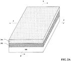
- FIG. 2A is a perspective view of a structure in step 101 of a manufacturing process of a semiconductor device.
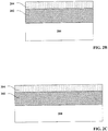
- FIG. 2B is a cross-sectional diagram that schematically illustrates a structure shown in FIG. 2A that is intercepted along a line A-A'.
- FIG. 2C is a cross-sectional diagram that schematically illustrates a structure shown in FIG. 2A that is intercepted along a line B-B'.
- an arrow related to the section line A-A' or B-B' represents a view direction.
- an initial substrate is provided, where the initial substrate structure may include a substrate and a first material layer 204 on the substrate.
- the substrate may include a substrate layer 200 and a first dielectric layer 202 on the substrate layer 200.
- the first material layer 204 may be above the first dielectric layer 202.
- the material of the substrate layer 200 may include a semiconductor material such as silicon.
- a material forming the first dielectric layer 202 may include an oxide of silicon.
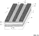
- FIG. 3A and FIG. 4A are perspective view that schematically illustrate a process of forming an nanowire according to a form of this application;
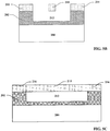
- FIG. 3B schematically illustrates a cross-sectional diagram intercepted along a line A-A' in FIG. 3A ;
- FIG. 3C schematically illustrates a cross-sectional diagram intercepted along a line B-B' in FIG. 3A ;
- FIG. 4B schematically illustrates a cross-sectional diagram intercepted along a line A-A' in FIG. 4A ;
- FIG. 4C schematically illustrates a cross-sectional diagram intercepted along a line B-B' in FIG. 4A .
- FIG. 4C schematically illustrates a cross-sectional diagram intercepted along a line B-B' in FIG. 4A .
- FIG. 4C schematically illustrates a cross-sectional diagram intercepted along a line B-B' in FIG. 4A .
- FIG. 4C schematically illustrates
- a first protection layer 206 and a patterned mask 208 may be successively formed on the first material layer 204.
- the material of the first protection layer 206 may include, for example, an oxide of silicon or a nitride of silicon.
- the first material layer 204 may be formed by materials such as polysilicon, or doped polysilicon or silicon germanium.
- the patterned mask may be formed by using a double patterning (double patterning) process, a self-assembly process, or a sidewall mask process.
- the first protection layer 206 and the first material layer 204 are etched by using a patterned first mask 208, so as to pattern the first material layer 204 to form a nanowire 210 (see FIG. 4A to FIG. 4C ). Then the patterned mask 208 and the first protection layer 206 may be removed. The obtained device structure is shown in FIG. 4A-4C .
- FIG. 4A and FIG. 4B a portion 211 obtained by patterning the first material layer 204 and is at two sides of the nanowire 210 is further shown. As shown in FIG. 4A and FIG. 4B , the portion 211 does not serve as a nanowire, but in other forms, the portion 211 may be formed as a nanowire.
- a first removing processing is performed to remove at least upper portions of the first dielectric layer 202 which are below the nanowire 210 and within regions at two sides along a length direction of the nanowire 210, so as to form a recess 212, as shown in FIG. 5A .
- portions of the first dielectric layer 202 which are located at two sides of the nanowire 210 may be first etched by using dry etching to be below the nanowire 210. Then wet etching is performed, and a portion of the first dielectric layer 202 that is below the nanowire 210 is removed, so as to form the recess 212.
- FIG. 5A is a perspective view that schematically illustrates a structure in which the recess 212 is formed in this way.
- FIG. 5B schematically illustrates a cross-sectional diagram intercepted along a line A-A' in FIG. 5A .
- FIG. 5C schematically illustrates a cross-sectional diagram intercepted along a line B-B' in FIG. 5A .
- the nanowire 210 may include a portion above the recess 212, and a support portion 216 above edges of two ends of the recess 212 (the first dielectric layer 202). It can be seen from FIG. 5C that the first material layer 204 includes the nanowire 210, and the nanowire 210 spans the recess 212 and is suspended above the recess 212. Therefore, in some forms, the term "nanowire" indicates, in combination with other appropriate definitions when necessary, a portion of the nanowire which spans the recess and is suspended above the recess. In the accompanying drawings, e.g., FIG. 5C , the portion of the nanowire which spans the recess and is suspended above the recess is marked by a reference numeral 210.
- the support portion 216 at two ends of the nanowire 210 may also extend along a width direction of the nanowire 210, i.e., the support portion 216 forms an "I" shape or an "H” shape (not shown in the figures) with the nanowire 210, where the nanowire 210 is a transverse connecting portion in the "H" shape.
- the first material layer 204 may further include a portion 216 at two ends of the recess 212 and above the first dielectric layer 202. Two ends of the nanowire 210 may be bonded or connected to the portion 216 of the first material 204 that is at the two ends of the recess 212 and above the first dielectric layer 202.
- a patterned mask shields the nanowire 210, and further shields at least a portion of the first material layer 204 that is bonded or connected to the nanowire 210.
- the recess 212 is shown as being formed in the first dielectric layer 202. However, in another specific form, the recess 212 may further extend through the first dielectric layer 202 into the substrate layer 200.
- step 103 a base layer is formed on the substrate structure.
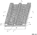
- FIG. 6A schematically illustrates a perspective view of a structure of a semiconductor device in step 103.
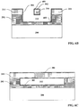
- FIG. 6B schematically illustrates a cross-sectional diagram of a structure shown in FIG. 6A that is intercepted along a line A-A'.
- FIG. 6C schematically illustrates a cross-sectional diagram of a structure shown in FIG. 6A that is intercepted along a line B-B'.
- a base layer 302 is formed on the substrate structure.
- the base layer 302 includes at least a first portion 601 covering an exposed surface of the nanowire 210 and a second portion 603 covering an exposed surface of the recess 212.
- the material of the base layer 302 may include an oxide of aluminum, and may alternatively include another material, known by a person skilled in the art, on which graphene can be selectively grown.
- the base layer 302 may be formed by using an atomic layer deposition process.
- step 105 a graphene layer is selectively grown on the base layer.
- FIG. 7A schematically illustrates a perspective view of a structure of a semiconductor device in step 105.
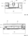
- FIG. 7B schematically illustrates a cross-sectional diagram of a structure shown in FIG. 7A that is intercepted along a line A-A'.
- FIG. 7C schematically illustrates a cross-sectional diagram of a structure shown in FIG. 7A that is intercepted along a line B-B'.
- a graphene layer 304 is selectively grown on the base layer 302.
- the graphene layer 304 may cover an exposed surface of the base layer 302, and include a first portion on a surface of the first portion of the base layer 302, and a second portion on a surface of the second portion of the base layer 302.
- the step of selectively growing the graphene layer 304 on the base layer 302 includes selectively growing the graphene layer 304 at a temperature of 900-1000°C by a chemical vapor deposition process using methane and hydrogen. It should be understood that the present invention is not limited thereto, but may also use other technologies for growing a graphene layer.
- step 107 a second dielectric layer is formed on the graphene layer.
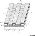
- FIG. 8A schematically illustrates a perspective view of a structure of a semiconductor device in step 107.
- FIG. 8B schematically illustrates a cross-sectional diagram of a structure shown in FIG. 8A that is intercepted along a line A-A'.
- FIG. 8C schematically illustrates a cross-sectional diagram of a structure shown in FIG. 8A that is intercepted along a line B-B'.
- a second dielectric layer 306 is formed on the graphene layer 304.
- the second dielectric layer 306 may cover an exposed surface of the graphene layer 304.
- the second dielectric layer 306 may include a first portion on a surface of the first portion of the graphene layer 304, and a second portion on a surface of the second portion of the graphene layer 304.
- the material of the second dielectric layer 306 may include boron nitride, an oxide of silicon, an oxide of hafnium, an oxide of aluminum, or a nitride of aluminum.
- the second dielectric layer 306 may be formed by using an atomic layer deposition process.
- step 109 after the second dielectric layer is formed, an electrode material layer is formed on the substrate structure to cover the second dielectric layer.
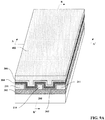
- FIG. 9A schematically illustrates a perspective view of a structure of a semiconductor device in step 109.
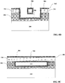
- FIG. 9B schematically illustrates a cross-sectional diagram of a structure shown in FIG. 9A that is intercepted along a line A-A'.
- FIG. 9C schematically illustrates a cross-sectional diagram of a structure shown in FIG. 9A that is intercepted along a line B-B'.
- an electrode material layer 402 is formed on the substrate structure to cover the second dielectric layer 306.
- the electrode material layer 402 is further formed to fill a space below the nanowire 210 and between the first portion of the second dielectric layer 306 and the second portion of the second dielectric layer 306 (i.e., the electrode material layer 402 fills the recess 212).
- the material of the electrode material layer 402 may include polysilicon.
- step 111 an active region defining processing is performed.
- the electrode material layer, the second dielectric layer, and the graphene layer are partially removed so as to define an area of an active region.
- at least a portion of a stack layer of the electrode material layer, the second dielectric layer, and the graphene layer on the nanowire is retained.
- FIG. 10A to FIG. 10C , FIG. 11A to FIG. 11C , and FIG. 12A to FIG. 12C show the active region defining processing according to an implementation of this disclosure.
- the step of performing the active region defining processing includes: forming a patterned mask 404 on the electrode material layer 402, as shown in FIG. 10A , FIG. 10B, and FIG. 10C .
- the patterned mask 404 may shield at least a portion of the nanowire 210.
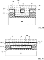
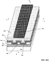
- FIG. 10A is a perspective view of a structure in which the patterned mask 404 is formed on the electrode material layer 402 according to a form of the present invention.
- FIG. 10B schematically illustrates a cross-sectional diagram intercepted along a line A-A' in FIG.
- FIG. 10C schematically illustrates a cross-sectional diagram intercepted along a line B-B' in FIG. 10A .
- the patterned mask 404 shields the nanowire 210 and the recess 212, as shown in FIG. 10A , FIG. 10B, and FIG. 10C .
- the patterned mask 404 may also merely shield the nanowire 210 and a portion of the recess 212 (not shown in the figures).
- the mask 404 may be formed to have a narrower lateral width than the mask 404 shown in FIG. 10B .
- portions of the electrode material layer 402, the second dielectric layer 306, and the graphene layer 304 that are not shielded by the patterned mask 404 are removed by using the patterned mask 404. That is, portions of the electrode material layer 402, the second dielectric layer 306, and the graphene layer 304 (for example, the portions of the electrode material layer 402, the second dielectric layer 306, and the graphene layer 304 that are not shielded by the patterned mask 404) are removed. So that, the area of the active region is defined. Then the patterned mask 404 may be removed. Perspective view of the obtained structure is shown in FIG. 11A .
- FIG. 11B and FIG. 11C are sectional diagrams of FIG.
- the stack layer of the electrode material layer 402, the second dielectric layer 306, and the graphene layer 304 that is in the recess 212 (or, on a surface of the recess 212) may be removed.
- the stack layer of the electrode material layer 402, the second dielectric layer 306, and the graphene layer 304 that is in the recess 212 (or, on a surface of the recess 212) may be retained.
- the first material layer 204 may further include a support portion 216 at two ends of the recess 212 and above the first dielectric layer 202, as described in one of the implementations regarding step 101.
- the patterned mask shields the nanowire 210, and further shields at least a portion of the first material layer 204 that is bonded or connected to the nanowire 210, for example, at least a portion of the support portion 216.
- the active region defining processing may further include a shaping step, so as to process a profile of the electrode material layer 402, as shown in FIG. 12A to FIG. 12C .
- a shaping step so as to process a profile of the electrode material layer 402, as shown in FIG. 12A to FIG. 12C .
- the profile of the electrode material layer 402 may be smoothened, and the recess 212 may be better filled.
- FIG. 12A shows a perspective view of a structure obtained after annealing processing is performed on the structure in FIG. 11A .
- FIG. 12B and FIG. 12C are cross-sectional diagrams of FIG. 12A intercepted along a line A-A' and a line B-B', respectively.
- the profile of the electrode material layer 402 is smooth.
- a gate defining processing is performed.
- the gate defining processing may include etching at least a portion of the stack layer to at least the second dielectric layer so as to form a gate structure surrounding an intermediate portion of the nanowire.
- the gate structure includes a portion of the electrode material layer and the second dielectric layer.
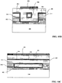
- the step of performing the gate defining processing may include: forming a third dielectric layer 502 to cover at least the substrate structure and the area of the active region, as shown in FIG. 13A and FIG. 13B.
- FIG. 13A and FIG. 13B show sectional diagrams that are intercepted along a transverse direction of the nanowire 210 (the nanowire 210 is above the recess) (for example, a direction of the line A-A' shown in the foregoing figures) and intercepted along a longitudinal direction of the nanowire 210 (for example, a direction of the line B-B' shown in the foregoing figures), respectively.
- the material of the third dielectric layer may include an oxide of silicon.
- the at least a portion of the stack layer of the electrode material layer, the second dielectric layer, and the graphene layer is etched to at least the second dielectric layer 306 by using a patterned mask 504.
- a gate structure surrounding an intermediate portion of the nanowire 210 is formed.
- the stack layer at a bottom portion of the recess 212 may be first etched by using dry etching, and then the electrode material layer 402 under a portion of the nanowire 210 that is in the recess 212 and is not shielded is etched, so that the gate structure is formed.
- the gate structure includes a portion of the electrode material layer and the second dielectric layer.
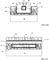
- the stack layer on a side wall of the recess 212 is etched and removed, as shown in FIG. 15A and FIG. 15B .
- the stack layer at the bottom portion and the side wall of the recess 212 may also be removed in subsequent steps.
- the electrode material layer 402 is used as a first gate, and the nanowire 210 covered by the electrode material layer 402 is used as a second gate.
- the method may further include a step of removing the stack layer at the bottom portion and the side wall of the recess 212.
- stack layer other than the bottom portion and the side wall of the recess 212 may be shielded by a patterned mask and the stack layer at the bottom portion and the side wall of the recess 212 may be removed using a dry etching process.
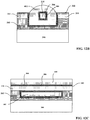
- Cross-sectional diagrams of the obtained structure are shown in FIG. 16A and FIG. 16B , respectively.
- the method may further include a step of removing the third dielectric layer 502. Moreover, a bottom portion of the electrode material layer is shaped, and a cross sectional profile of the shaped electrode material layer 402 is circular, as shown in the perspective view of the obtained structure of FIG. 17 .
- the method may further include step 115, which is a step of forming a contact component.
- a fourth dielectric layer 1701 may further be formed, so as to at least cover the substrate structure and the area of the active region.
- a material forming the fourth dielectric layer may include an oxide of silicon.
- a hole 1703 through the fourth dielectric layer and the second dielectric layer 306 to the graphene layer 304 is formed.
- the hole 1703 (not shown in the figures, filled with 1075) is separated from the gate structure.
- the hole is filled with a conductive material, so as to form a contact component 1705 to the graphene layer (i.e., may be an electrode contact component to a source/drain region).
- FIG. 18A shows that the contact component 1705 is located at the support portion 216 which is at the two ends of the nanowire 210 and is bonded thereto.
- a person skilled in the art may adjust the position of the contact component 1705 according to various requirements.
- the contact component 1705 may be conceived to be located at the nanowire (the nanowire crosses above the recess).
- a doped nanowire 210 may be used as the second gate (or, a back gate), as stated above.
- a fourth dielectric layer may be formed to at least cover the substrate structure and the area of the active region.
- a material forming the fourth dielectric layer may include an oxide of silicon.
- a hole running through the fourth dielectric layer, the second dielectric layer 306, and the graphene layer 304 to the first material layer 204 (the nanowire 210) is formed.
- an insulating material layer 1707 is formed on a side wall of the hole.
- the hole is filled with a conductive material so as to form a contact component 1709 to at least a portion of the first material layer 204.
- the hole is filled with a conductive material so as to form a contact component to the first material layer (i.e., a second gate contact component), as shown in FIG. 18B .
- the step of forming the contact component may include: forming a fourth dielectric layer, where the fourth dielectric layer at least covers the substrate structure and the area of the active region.
- a material forming the fourth dielectric layer may include an oxide of silicon.
- a hole passing through the fourth dielectric layer, the second dielectric layer 306, and the graphene layer 304 to at least a portion of the first material layer 204 is formed.
- an insulating material layer is formed on a side wall of the hole.
- the hole is filled with a conductive material so as to form a contact component to the at least a portion of the first material layer, where the insulating material layer electrically isolates the graphene layer from the contact component.
- a new method for manufacturing a semiconductor device that introduces graphene is provided.
- the operating current is better controlled and performances of a device are improved.
- this disclosure further teaches a semiconductor device, including: a substrate structure, the substrate structure including a substrate and a first material layer on the substrate, a recess being formed in the substrate, the first material layer including a nanowire, and the nanowire spanning the recess and being suspended above the recess; a base layer on an exposed surface of the nanowire; a graphene layer on the base layer; a second dielectric layer on the graphene layer; and a gate structure surrounding an intermediate portion of the nanowire, where the gate structure includes a portion of the electrode material layer and the second dielectric layer.
- the substrate includes a substrate layer and a first dielectric layer on the substrate layer, the first material layer being on the first dielectric layer, and the recess being formed in the first dielectric layer.
- the recess further extends through the first dielectric layer into the substrate layer.
- the gate structure further includes a portion in the recess below the nanowire.
- the first material layer further includes a portion above the first dielectric layer at two ends of the recess, the two ends of the recess being bonded to the portion of the first material layer.
- the first material layer is formed by polysilicon, or doped polysilicon or silicon germanium; the material of the base layer includes an oxide of aluminum; the material of the first dielectric layer includes an oxide of silicon; and the material of the second dielectric layer includes boron nitride, an oxide of silicon, an oxide of hafnium, an oxide of aluminum, or a nitride of aluminum.
- the graphene layer is selectively grown on the base layer.
- the nanowire is formed by doped polysilicon; and the portion of the electrode material layer that is included in the gate structure is used as a first gate, and the nanowire is used as a second gate.
- the device further includes: a second base layer on an exposed surface of the recess; a second graphene layer on the base layer; and a second dielectric layer on the second graphene layer, where the base layer is integrally formed with the second base layer, the graphene layer is integrally formed with the second graphene layer, and the second dielectric layer is integrally formed with the second dielectric layer.
- the device further includes: a fourth dielectric layer, at least covering the substrate structure and the nanowire on which a stack layer of the base layer, the graphene layer, and the second dielectric layer is formed; a hole running through the fourth dielectric layer and the second dielectric layer to the graphene layer; and a contact component filling the hole and to the graphene layer.
- the device further includes: a fourth dielectric layer, at least covering the substrate structure and the nanowire on which a stack layer of the base layer, the graphene layer, and the second dielectric layer is formed; a hole running through the fourth dielectric layer, the second dielectric layer, and the graphene layer to the first material layer; an insulating material layer on a side wall of the hole; and a contact component filling the hole and to the first material layer, where the insulating material layer electrically isolates the graphene layer from the contact component.
- the device further includes: a fourth dielectric layer, at least covering the substrate structure and the nanowire on which a stack layer of the base layer, the graphene layer, and the second dielectric layer is formed; a hole running through the fourth dielectric layer, the second dielectric layer, and the graphene layer to the portion of the first material layer; and a contact component which is formed to the at least a portion of the first material layer by filling the hole with a conductive material.
Landscapes
- Thin Film Transistor (AREA)
- Physics & Mathematics (AREA)
- Geometry (AREA)
- Semiconductor Memories (AREA)
Abstract
Description
- This application is based on and claims priority to Chinese patent Application
CN201610871339.8 - The present invention relates to the field of semiconductors, particularly to a semiconductor device and a manufacturing method therefor, and more particularly to a graphene semiconductor device and a manufacturing method therefor.
- With the constant development of semiconductor technologies, the size of semiconductor devices becomes smaller. The size of semiconductor devices based on silicon materials has evolved according to the Moore's Law for about 40 years. The Complementary Metal Oxide Semiconductor (CMOS for short) technology can almost be considered as the cornerstone of the development of the global information technologies. Semiconductor devices based on silicon materials will still be the mainstream of the development of semiconductor technologies at least for an indefinitely long period of time in the future. However, to ensure that the semiconductor technologies can continue to evolve according to the Moore's Law, only reducing the device size proportionally cannot sufficiently meet the requirements. Therefore, new materials need to be introduced into the existing CMOS manufacturing process, so as to further lower the production and manufacturing costs, improve the device performance, and reduce power consumption due to leakage current. Graphene-based electronic devices are considered to be one of the candidate solutions for semiconductor devices.
- It is an object of the present invention to provide a method for manufacturing a semiconductor device and a semiconductor device which address at least one of the foregoing problems.
- The object is achieved by the features of the respective independent claims. Further embodiments are defined in the respective dependent claims.
- A first aspect of the present invention provides a method for manufacturing a semiconductor device. The method includes: providing a substrate structure, including a substrate and a first material layer on the substrate, wherein a recess is formed in the substrate and the first material layer includes a nanowire spanning and suspended above the recess; forming a base layer on the substrate structure, where the base layer includes at least a first portion covering an exposed surface of the nanowire and a second portion covering an exposed surface of the recess; selectively growing a graphene layer on the base layer; forming a second dielectric layer on the graphene layer; forming an electrode material layer on the substrate structure to cover the second dielectric layer; partially removing the electrode material layer, the second dielectric layer, and the graphene layer so as to define an area of an active region wherein at least a portion of a stack layer of the electrode material layer, the second dielectric layer, and the graphene layer on the nanowire remains and is within the active region; and forming a gate by etching at least a portion of the remaining stack layer within the active region to at least the second dielectric layer so as to form a gate structure surrounding an intermediate portion of the nanowire, where the gate structure includes a portion of the electrode material layer and the second dielectric layer.
- Preferably, after defining the gate, the method further includes: removing portions of the graphene layer and the second dielectric layer on a surface of the recess.
- Preferably, defining the active region includes: forming a patterned mask on the electrode material layer, the patterned mask shielding at least a portion of the nanowire; and removing, by using the patterned mask, portions of the electrode material layer, the second dielectric layer, and the graphene layer not shielded by the patterned mask.
- Preferably, the patterned mask shields the nanowire and at least a portion of the recess.
- Preferably, the substrate includes a substrate layer and a first dielectric layer on the substrate layer, wherein the first material layer is on the first dielectric layer; the recess is formed in the first dielectric layer; and providing a substrate structure includes: providing an initial substrate structure including the substrate and the first material layer on the first dielectric layer; patterning the first material layer to define a region covering the nanowire and two sides of the nanowire along the length direction of the nanowire; and removing at least upper portions of the first dielectric layer of the defined region to form the recess.
- Preferably, the recess further extends through the first dielectric layer into the substrate layer.
- Preferably, the graphene layer includes a first portion on a surface of the first portion of the base layer, and a second portion on a surface of the second portion of the base layer; the second dielectric layer includes a first portion on a surface of the first portion of the graphene layer, and a second portion on a surface of the second portion of the graphene layer; and wherein the electrode material layer is further formed to fill a space below the nanowire and between the first portion of the second dielectric layer and the second portion of the second dielectric layer when forming the electrode material layer.
- Preferably, the first material layer further includes a portion above the first dielectric layer at two ends of the recess bonded to the portion of the first material layer forming the nanowire; and the patterned mask shields the nanowire, and further shields at least a portion of the first material layer that is bonded to the nanowire.
- Preferably, the first material layer comprises polysilicon, doped polysilicon, or silicon germanium; the base layer comprises an oxide of aluminum; the first dielectric layer comprises an oxide of silicon; and the second dielectric layer comprises boron nitride, an oxide of silicon, an oxide of hafnium, an oxide of aluminum, or a nitride of aluminum.
- Preferably, the material of the base layer includes an oxide of aluminum, and selectively growing the graphene layer on the base layer includes selectively growing the graphene layer at a temperature of 900-1000°C by a chemical vapor deposition process using methane and hydrogen.
- Preferably, the nanowire comprises doped polysilicon; and the portion of the electrode material layer in the gate structure is used as a first gate, and the nanowire is used as a second gate.
- Preferably, forming the gate includes: forming a third dielectric layer to cover at least the substrate structure and the area of the active region; and etching, by using a patterned mask defining a gate area, a portion of the third dielectric layer outside the gate area and at least a portion of the stack layer within the active region but outside the gate area to at least the second dielectric layer so as to form a gate structure surrounding an intermediate portion of the nanowire, where the gate structure includes a portion of the electrode material layer and the second dielectric layer.
- In a first variant, the method further includes: forming a fourth dielectric layer to at least cover the substrate structure and the area of the active region; forming a hole through the fourth dielectric layer and the second dielectric layer to the graphene layer, the hole being separated from the gate structure; and filling the hole with a conductive material, so as to form a contact component to the graphene layer.
- In a second variant, after the gate defining processing, the method further includes: forming a fourth dielectric layer to at least cover the substrate structure and the area of the active region; forming a hole through the fourth dielectric layer, the second dielectric layer, and the graphene layer to the first material layer; forming an insulating material layer on a side wall of the hole; and after the insulating material layer is formed, filling the hole with a conductive material so as to form a contact component to the first material layer.
- In a third variant, the method further includes: forming a fourth dielectric layer to at least cover the substrate structure and the area of the active region; forming a hole through the fourth dielectric layer, the second dielectric layer, and the graphene layer to the at least a portion of the first material layer; forming an insulating material layer on a side wall of the hole; and after the insulating material layer is formed, filling the hole with a conductive material so as to form a contact component to the at least a portion of the first material layer, where the insulating material layer electrically isolates the graphene layer from the contact component.
- A second aspect of the present invention provides a semiconductor device. The semiconductor device includes: a substrate structure including a substrate and a first material layer on the substrate, and a recess formed in the substrate, wherein the first material layer comprises a nanowire spanning and suspended above the recess; a base layer on an exposed surface of the nanowire; a graphene layer on the base layer; a second dielectric layer on the graphene layer; and a gate structure surrounding an intermediate portion of the nanowire, where the gate structure includes a portion of the electrode material layer and the second dielectric layer surrounding the portion of the second dielectric layer.
- Preferably, the substrate includes a substrate layer and a first dielectric layer on the substrate layer, wherein the first material layer is on the first dielectric layer, and the recess is formed in the first dielectric layer.
- Preferably, the recess further extends through the first dielectric layer into the substrate layer.
- Preferably, the gate structure further includes a portion in the recess below the nanowire.
- Preferably, the first material layer further includes a portion above the first dielectric layer at two ends of the recess bonded to the portion of the first material layer forming the nanowire.
- Preferably, the first material layer comprises polysilicon, doped polysilicon, or silicon germanium; the base layer comprises an oxide of aluminum; the first dielectric layer comprises an oxide of silicon; and the second dielectric layer comprises boron nitride, an oxide of silicon, an oxide of hafnium, an oxide of aluminum, or a nitride of aluminum.
- Preferably, the graphene layer is selectively grown on the base layer.
- Preferably, the nanowire comprises doped polysilicon; and the portion of the electrode material layer in the gate structure is used as a first gate, and the nanowire is used as a second gate.
- Preferably, the device further includes: a second base layer on an exposed surface of the recess; a second graphene layer on the second base layer; and a second dielectric layer on the second graphene layer, where the base layer is integrally formed with the second base layer, the graphene layer is integrally formed with the second graphene layer, and the second dielectric layer is integrally formed with the second dielectric layer.
- In a first variant, the device further includes: a fourth dielectric layer, covering at least the substrate structure and the nanowire on which a stack layer of the base layer, the graphene layer, and the second dielectric layer is formed; a hole through the fourth dielectric layer and the second dielectric layer to the graphene layer; and a contact component filling the hole and to the graphene layer.
- In a second variant, the device further includes: a fourth dielectric layer, covering at least the substrate structure and the nanowire on which a stack layer of the base layer, the graphene layer, and the second dielectric layer is formed; a hole through the fourth dielectric layer, the second dielectric layer, and the graphene layer to the first material layer; an insulating material layer on a side wall of the hole; and a contact component filling the hole and to the first material layer, where the insulating material layer electrically isolates the graphene layer from the contact component.
- In a third variant, the device further includes: a fourth dielectric layer, covering at least the substrate structure and the nanowire on which a stack layer of the base layer, the graphene layer, and the second dielectric layer is formed; a hole through the fourth dielectric layer, the second dielectric layer, and the graphene layer to the portion of the first material layer; and a contact component which is formed to the at least a portion of the first material layer by filling the hole with a conductive material.
- According to the following detailed descriptions of the forms of implementations for illustration purposes of the present invention with reference to the accompanying drawings, other characters and advantages of the present invention will become clear.
- The accompanying drawings that form a part of the specification describe forms of the present invention, and are used to explain the principles of the present invention together with the specification.
- With reference to the accompanying drawings, the present invention can be understood more clearly according to the following detailed description, where:
-
FIG. 1 is a schematic flowchart of a method for manufacturing a semiconductor device; -
FIG. 2A is a perspective view of a structure at a phase of a manufacturing process of a semiconductor device; -
FIG. 2B schematically illustrates a cross-sectional diagram intercepted along a line A-A' inFIG. 2A ; -
FIG. 2C schematically illustrates a cross-sectional diagram intercepted along a line B-B' inFIG. 2A ; -
FIG. 3A is a perspective view of a structure at a phase of a manufacturing process of a semiconductor device; -
FIG. 3B schematically illustrates a cross-sectional diagram intercepted along a line A-A' inFIG. 3A ; -
FIG. 3C schematically illustrates a cross-sectional diagram intercepted along a line B-B' inFIG. 3A ; -
FIG. 4A is a perspective view of a structure at a phase of a manufacturing process of a semiconductor device; -
FIG. 4B schematically illustrates a cross-sectional diagram intercepted along a line A-A' inFIG. 4A ; -
FIG. 4C schematically illustrates a cross-sectional diagram intercepted along a line B-B' inFIG. 4A ; -
FIG. 5A is a perspective view of a structure at a phase of a manufacturing process of a semiconductor device; -
FIG. 5B schematically illustrates a cross-sectional diagram intercepted along a line A-A' inFIG. 5A ; -
FIG. 5C schematically illustrates a cross-sectional diagram intercepted along a line B-B' inFIG. 5A ; -
FIG. 6A is a perspective view of a structure at a phase of a manufacturing process of a semiconductor device; -
FIG. 6B schematically illustrates a cross-sectional diagram intercepted along a line A-A' inFIG. 6A ; -
FIG. 6C schematically illustrates a cross-sectional diagram intercepted along a line B-B' inFIG. 6A ; -
FIG. 7A is a perspective view of a structure at a phase of a manufacturing process of a semiconductor device; -
FIG. 7B schematically illustrates a cross-sectional diagram intercepted along a line A-A' inFIG. 7A ; -
FIG. 7C schematically illustrates a cross-sectional diagram intercepted along a line B-B' inFIG. 7A ; -
FIG. 8A is a perspective view of a structure at a phase of a manufacturing process of a semiconductor device; -
FIG. 8B schematically illustrates a cross-sectional diagram intercepted along a line A-A' inFIG. 8A ; -
FIG. 8C schematically illustrates a cross-sectional diagram intercepted along a line B-B' inFIG. 8A ; -
FIG. 9A is a perspective view of a structure at a phase of a manufacturing process of a semiconductor device; -
FIG. 9B schematically illustrates a cross-sectional diagram intercepted along a line A-A' inFIG. 9A ; -
FIG. 9C schematically illustrates a cross-sectional diagram intercepted along a line B-B' inFIG. 9A ; -
FIG. 10A is a perspective view of a structure at a phase of a manufacturing process of a semiconductor device; -
FIG. 10B schematically illustrates a cross-sectional diagram intercepted along a line A-A' inFIG. 10A ; -
FIG. 10C schematically illustrates a cross-sectional diagram intercepted along a line B-B' inFIG. 10A ; -
FIG. 11A is a perspective view of a structure at a phase of a manufacturing process of a semiconductor device; -
FIG. 11B schematically illustrates a cross-sectional diagram intercepted along a line A-A' inFIG. 11A ; -
FIG. 11C schematically illustrates a cross-sectional diagram intercepted along a line B-B' inFIG. 11A ; -
FIG. 12A is a perspective view of a structure at a phase of a manufacturing process of a semiconductor device; -
FIG. 12B schematically illustrates a cross-sectional diagram intercepted along a line A-A' inFIG. 12A ; -
FIG. 12C schematically illustrates a cross-sectional diagram intercepted along a line B-B' inFIG. 12A ; -
FIG. 13A and FIG. 13B are schematic diagrams that illustrate cross sections of a structure at a phase of a manufacturing process of a semiconductor device; -
FIG. 14A and FIG. 14B are schematic diagrams that illustrate cross sections of a structure at a phase of a manufacturing process of a semiconductor device; -
FIG. 15A and FIG. 15B are schematic diagrams that illustrate cross sections of a structure at a phase of a manufacturing process of a semiconductor device; -
FIG. 16A and FIG. 16B are schematic diagrams that illustrate cross sections of a structure at a phase of a manufacturing process of a semiconductor device; -
FIG. 17 is a perspective view of a structure at a phase of a manufacturing process of a semiconductor device; and -
FIG. 18A and FIG. 18B are schematic diagrams that illustrate cross sections of a structure at a phase of a manufacturing process of a semiconductor device. - Various exemplary forms or implementations for illustration purposes of the present invention are described in details with reference to the accompanying drawings. It should be noted that unless being described in detail, relative layouts, mathematical expressions, and numeric values of components and steps described in these forms do not limit the present invention.
- Meanwhile, it should be noted that for convenience of description, sizes of the parts shown in the accompanying drawings may not be drawn according to an actual proportional relationship.
- The following description about at least one exemplary form is illustrative only, and would not be used as any limitation on the present invention and applications or uses of the present invention.
- Technologies, methods, and devices that are known by a person of ordinary skill in the related art may not be discussed in detail. However, if appropriate, these technologies, methods, and devices should be considered as a part of the description.
- In all examples shown and discussed herein, any specific value should be interpreted to be illustrative only rather than a limitation. Therefore, other examples of the forms may have different values.
- It should be noted that the term "semiconductor device", used in a general sense and when there is no other specific limitations, includes any device operating partly or entirely based on semiconductor principles, including but not limited to: various semiconductor elements such as a diode, a bipolar transistor, and a field effect transistor; an integrated or discrete circuit, die, or chip composed of various semiconductor elements; and any device of the foregoing element, circuit, die, or chip. However, it should be further noted that this term may be specifically limited: in different exemplary forms, the term "semiconductor device" may be limited, by other definitions which are relevant to this term, by explicitly description in the context, or by requirement of operating principles, to particular semiconductor elements, circuits, dies, chips, or devices only.
- It should be noted that similar reference numerals, labels, and letters represent similar items in the following accompanying drawings. Therefore, once an item is defined in a figure, the item needs not to be further discussed in subsequent figures.
-
FIG. 1 is a schematic flowchart of a method for manufacturing a semiconductor device.FIG. 2A to FIG. 16B are schematic diagrams that illustrate a plurality of phases of a manufacturing process of a semiconductor device. Description is made in the following with reference toFIG. 1 andFIG. 2A toFIG. 16B . - As shown in
FIG. 1 , instep 101, a substrate structure is provided. -
FIG. 2A is a perspective view of a structure instep 101 of a manufacturing process of a semiconductor device.FIG. 2B is a cross-sectional diagram that schematically illustrates a structure shown inFIG. 2A that is intercepted along a line A-A'.FIG. 2C is a cross-sectional diagram that schematically illustrates a structure shown inFIG. 2A that is intercepted along a line B-B'. Herein, it should be noted that in the accompanying drawings, an arrow related to the section line A-A' or B-B' represents a view direction. - As shown in
FIG. 2A ,FIG. 2B, and FIG. 2C , an initial substrate is provided, where the initial substrate structure may include a substrate and afirst material layer 204 on the substrate. - In an implementation, the substrate may include a
substrate layer 200 and a firstdielectric layer 202 on thesubstrate layer 200. In such a situation, thefirst material layer 204 may be above thefirst dielectric layer 202. The material of thesubstrate layer 200 may include a semiconductor material such as silicon. A material forming thefirst dielectric layer 202 may include an oxide of silicon. - Subsequently, the first material layer is patterned to form a nanowire.
FIG. 3A andFIG. 4A are perspective view that schematically illustrate a process of forming an nanowire according to a form of this application;FIG. 3B schematically illustrates a cross-sectional diagram intercepted along a line A-A' inFIG. 3A ;FIG. 3C schematically illustrates a cross-sectional diagram intercepted along a line B-B' inFIG. 3A ;FIG. 4B schematically illustrates a cross-sectional diagram intercepted along a line A-A' inFIG. 4A ; andFIG. 4C schematically illustrates a cross-sectional diagram intercepted along a line B-B' inFIG. 4A . As shown inFIG. 3A ,FIG. 3B, and FIG. 3C , afirst protection layer 206 and apatterned mask 208 may be successively formed on thefirst material layer 204. The material of thefirst protection layer 206 may include, for example, an oxide of silicon or a nitride of silicon. Thefirst material layer 204 may be formed by materials such as polysilicon, or doped polysilicon or silicon germanium. The patterned mask may be formed by using a double patterning (double patterning) process, a self-assembly process, or a sidewall mask process. Subsequently, thefirst protection layer 206 and thefirst material layer 204 are etched by using a patternedfirst mask 208, so as to pattern thefirst material layer 204 to form a nanowire 210 (seeFIG. 4A to FIG. 4C ). Then the patternedmask 208 and thefirst protection layer 206 may be removed. The obtained device structure is shown inFIG. 4A-4C . - It should be noted that in
FIG. 4A andFIG. 4B , aportion 211 obtained by patterning thefirst material layer 204 and is at two sides of thenanowire 210 is further shown. As shown inFIG. 4A andFIG. 4B , theportion 211 does not serve as a nanowire, but in other forms, theportion 211 may be formed as a nanowire. - Subsequently, a first removing processing is performed to remove at least upper portions of the
first dielectric layer 202 which are below thenanowire 210 and within regions at two sides along a length direction of thenanowire 210, so as to form arecess 212, as shown inFIG. 5A . In a specific form, portions of thefirst dielectric layer 202 which are located at two sides of thenanowire 210 may be first etched by using dry etching to be below thenanowire 210. Then wet etching is performed, and a portion of thefirst dielectric layer 202 that is below thenanowire 210 is removed, so as to form therecess 212.FIG. 5A is a perspective view that schematically illustrates a structure in which therecess 212 is formed in this way.FIG. 5B schematically illustrates a cross-sectional diagram intercepted along a line A-A' inFIG. 5A .FIG. 5C schematically illustrates a cross-sectional diagram intercepted along a line B-B' inFIG. 5A . - In addition, as shown in
FIG. 5A ,FIG. 5B, and FIG. 5C , along a length direction of thenanowire 210, thenanowire 210 may include a portion above therecess 212, and asupport portion 216 above edges of two ends of the recess 212 (the first dielectric layer 202). It can be seen fromFIG. 5C that thefirst material layer 204 includes thenanowire 210, and thenanowire 210 spans therecess 212 and is suspended above therecess 212. Therefore, in some forms, the term "nanowire" indicates, in combination with other appropriate definitions when necessary, a portion of the nanowire which spans the recess and is suspended above the recess. In the accompanying drawings, e.g.,FIG. 5C , the portion of the nanowire which spans the recess and is suspended above the recess is marked by areference numeral 210. - In a specific form, the
support portion 216 at two ends of thenanowire 210 may also extend along a width direction of thenanowire 210, i.e., thesupport portion 216 forms an "I" shape or an "H" shape (not shown in the figures) with thenanowire 210, where thenanowire 210 is a transverse connecting portion in the "H" shape. That is, thefirst material layer 204 may further include aportion 216 at two ends of therecess 212 and above thefirst dielectric layer 202. Two ends of thenanowire 210 may be bonded or connected to theportion 216 of thefirst material 204 that is at the two ends of therecess 212 and above thefirst dielectric layer 202. In this implementation, instep 111 described in the following, a patterned mask shields thenanowire 210, and further shields at least a portion of thefirst material layer 204 that is bonded or connected to thenanowire 210. - In addition, in
FIG. 5A to FIG. 5C , therecess 212 is shown as being formed in thefirst dielectric layer 202. However, in another specific form, therecess 212 may further extend through thefirst dielectric layer 202 into thesubstrate layer 200. - Subsequently, as shown in
FIG. 1 , instep 103, a base layer is formed on the substrate structure. -
FIG. 6A schematically illustrates a perspective view of a structure of a semiconductor device instep 103.FIG. 6B schematically illustrates a cross-sectional diagram of a structure shown inFIG. 6A that is intercepted along a line A-A'.FIG. 6C schematically illustrates a cross-sectional diagram of a structure shown inFIG. 6A that is intercepted along a line B-B'. As shown inFIG. 6A ,FIG. 6B, and FIG. 6C , abase layer 302 is formed on the substrate structure. Thebase layer 302 includes at least afirst portion 601 covering an exposed surface of thenanowire 210 and asecond portion 603 covering an exposed surface of therecess 212. The material of thebase layer 302 may include an oxide of aluminum, and may alternatively include another material, known by a person skilled in the art, on which graphene can be selectively grown. Thebase layer 302 may be formed by using an atomic layer deposition process. - Subsequently, as shown in
Fig. 1 , instep 105, a graphene layer is selectively grown on the base layer. -
FIG. 7A schematically illustrates a perspective view of a structure of a semiconductor device instep 105.FIG. 7B schematically illustrates a cross-sectional diagram of a structure shown inFIG. 7A that is intercepted along a line A-A'.FIG. 7C schematically illustrates a cross-sectional diagram of a structure shown inFIG. 7A that is intercepted along a line B-B'. As shown inFIG. 7A ,FIG. 7B, and FIG. 7C , agraphene layer 304 is selectively grown on thebase layer 302. Correspondingly, thegraphene layer 304 may cover an exposed surface of thebase layer 302, and include a first portion on a surface of the first portion of thebase layer 302, and a second portion on a surface of the second portion of thebase layer 302. - In a specific form, the step of selectively growing the
graphene layer 304 on thebase layer 302 includes selectively growing thegraphene layer 304 at a temperature of 900-1000°C by a chemical vapor deposition process using methane and hydrogen. It should be understood that the present invention is not limited thereto, but may also use other technologies for growing a graphene layer. - Subsequently, as shown in
Fig. 1 , instep 107, a second dielectric layer is formed on the graphene layer. -
FIG. 8A schematically illustrates a perspective view of a structure of a semiconductor device instep 107.FIG. 8B schematically illustrates a cross-sectional diagram of a structure shown inFIG. 8A that is intercepted along a line A-A'.FIG. 8C schematically illustrates a cross-sectional diagram of a structure shown inFIG. 8A that is intercepted along a line B-B'. As shown inFIG. 8A ,FIG. 8B, and FIG. 8C , asecond dielectric layer 306 is formed on thegraphene layer 304. Thesecond dielectric layer 306 may cover an exposed surface of thegraphene layer 304. Correspondingly, thesecond dielectric layer 306 may include a first portion on a surface of the first portion of thegraphene layer 304, and a second portion on a surface of the second portion of thegraphene layer 304. The material of thesecond dielectric layer 306 may include boron nitride, an oxide of silicon, an oxide of hafnium, an oxide of aluminum, or a nitride of aluminum. Thesecond dielectric layer 306 may be formed by using an atomic layer deposition process. - Subsequently, as shown in
Fig. 1 , instep 109, after the second dielectric layer is formed, an electrode material layer is formed on the substrate structure to cover the second dielectric layer. -
FIG. 9A schematically illustrates a perspective view of a structure of a semiconductor device instep 109.FIG. 9B schematically illustrates a cross-sectional diagram of a structure shown inFIG. 9A that is intercepted along a line A-A'.FIG. 9C schematically illustrates a cross-sectional diagram of a structure shown inFIG. 9A that is intercepted along a line B-B'. In an implementation, as shown inFIG. 9A ,FIG. 9B, and FIG. 9C , after thesecond dielectric layer 306 is formed, anelectrode material layer 402 is formed on the substrate structure to cover thesecond dielectric layer 306. Theelectrode material layer 402 is further formed to fill a space below thenanowire 210 and between the first portion of thesecond dielectric layer 306 and the second portion of the second dielectric layer 306 (i.e., theelectrode material layer 402 fills the recess 212). The material of theelectrode material layer 402 may include polysilicon. - Subsequently, as shown in
FIG. 1 , instep 111, an active region defining processing is performed. The electrode material layer, the second dielectric layer, and the graphene layer are partially removed so as to define an area of an active region. Moreover, within the area of the active region, at least a portion of a stack layer of the electrode material layer, the second dielectric layer, and the graphene layer on the nanowire is retained. -
FIG. 10A to FIG. 10C ,FIG. 11A to FIG. 11C , andFIG. 12A to FIG. 12C show the active region defining processing according to an implementation of this disclosure. In this implementation, the step of performing the active region defining processing includes: forming apatterned mask 404 on theelectrode material layer 402, as shown inFIG. 10A ,FIG. 10B, and FIG. 10C . The patternedmask 404 may shield at least a portion of thenanowire 210.FIG. 10A is a perspective view of a structure in which the patternedmask 404 is formed on theelectrode material layer 402 according to a form of the present invention.FIG. 10B schematically illustrates a cross-sectional diagram intercepted along a line A-A' inFIG. 10A .FIG. 10C schematically illustrates a cross-sectional diagram intercepted along a line B-B' inFIG. 10A . In this form, the patternedmask 404 shields thenanowire 210 and therecess 212, as shown inFIG. 10A ,FIG. 10B, and FIG. 10C . - In another specific form, the patterned
mask 404 may also merely shield thenanowire 210 and a portion of the recess 212 (not shown in the figures). For example, themask 404 may be formed to have a narrower lateral width than themask 404 shown inFIG. 10B . - Then, portions of the
electrode material layer 402, thesecond dielectric layer 306, and thegraphene layer 304 that are not shielded by the patternedmask 404 are removed by using the patternedmask 404. That is, portions of theelectrode material layer 402, thesecond dielectric layer 306, and the graphene layer 304 (for example, the portions of theelectrode material layer 402, thesecond dielectric layer 306, and thegraphene layer 304 that are not shielded by the patterned mask 404) are removed. So that, the area of the active region is defined. Then the patternedmask 404 may be removed. Perspective view of the obtained structure is shown inFIG. 11A .FIG. 11B and FIG. 11C are sectional diagrams ofFIG. 11A intercepted along a line A-A' and a line B-B', respectively. Within the area of the active region, at least a portion of a stack layer, on thenanowire 210, of theelectrode material layer 402, thesecond dielectric layer 306, and thegraphene layer 304 is retained. - In some forms, the stack layer of the
electrode material layer 402, thesecond dielectric layer 306, and thegraphene layer 304 that is in the recess 212 (or, on a surface of the recess 212) may be removed. However, in some other forms, the stack layer of theelectrode material layer 402, thesecond dielectric layer 306, and thegraphene layer 304 that is in the recess 212 (or, on a surface of the recess 212) may be retained. - In another implementation, the
first material layer 204 may further include asupport portion 216 at two ends of therecess 212 and above thefirst dielectric layer 202, as described in one of theimplementations regarding step 101. In some forms, the patterned mask shields thenanowire 210, and further shields at least a portion of thefirst material layer 204 that is bonded or connected to thenanowire 210, for example, at least a portion of thesupport portion 216. - Preferably, the active region defining processing may further include a shaping step, so as to process a profile of the
electrode material layer 402, as shown inFIG. 12A to FIG. 12C . For example, through annealing, the profile of theelectrode material layer 402 may be smoothened, and therecess 212 may be better filled.FIG. 12A shows a perspective view of a structure obtained after annealing processing is performed on the structure inFIG. 11A .FIG. 12B and FIG. 12C are cross-sectional diagrams ofFIG. 12A intercepted along a line A-A' and a line B-B', respectively. As shown in figures, the profile of theelectrode material layer 402 is smooth. - Subsequently, as shown in
FIG. 1 , instep 113, a gate defining processing is performed. The gate defining processing may include etching at least a portion of the stack layer to at least the second dielectric layer so as to form a gate structure surrounding an intermediate portion of the nanowire. The gate structure includes a portion of the electrode material layer and the second dielectric layer. - In an implementation, the step of performing the gate defining processing may include: forming a third
dielectric layer 502 to cover at least the substrate structure and the area of the active region, as shown inFIG. 13A and FIG. 13B. FIG. 13A and FIG. 13B show sectional diagrams that are intercepted along a transverse direction of the nanowire 210 (thenanowire 210 is above the recess) (for example, a direction of the line A-A' shown in the foregoing figures) and intercepted along a longitudinal direction of the nanowire 210 (for example, a direction of the line B-B' shown in the foregoing figures), respectively. The material of the third dielectric layer may include an oxide of silicon. - Subsequently, for example, as shown in
FIG. 14A and FIG. 14B , the at least a portion of the stack layer of the electrode material layer, the second dielectric layer, and the graphene layer is etched to at least thesecond dielectric layer 306 by using a patternedmask 504. As such, a gate structure surrounding an intermediate portion of thenanowire 210 is formed. For example, the stack layer at a bottom portion of therecess 212 may be first etched by using dry etching, and then theelectrode material layer 402 under a portion of thenanowire 210 that is in therecess 212 and is not shielded is etched, so that the gate structure is formed. The gate structure includes a portion of the electrode material layer and the second dielectric layer. In a form, during this etching, the stack layer on a side wall of therecess 212 is etched and removed, as shown inFIG. 15A and FIG. 15B . In another form, the stack layer at the bottom portion and the side wall of therecess 212 may also be removed in subsequent steps. In an implementation, theelectrode material layer 402 is used as a first gate, and thenanowire 210 covered by theelectrode material layer 402 is used as a second gate. - Optionally, the method may further include a step of removing the stack layer at the bottom portion and the side wall of the
recess 212. For example, stack layer other than the bottom portion and the side wall of therecess 212 may be shielded by a patterned mask and the stack layer at the bottom portion and the side wall of therecess 212 may be removed using a dry etching process. Cross-sectional diagrams of the obtained structure are shown inFIG. 16A and FIG. 16B , respectively. - Optionally, the method may further include a step of removing the third
dielectric layer 502. Moreover, a bottom portion of the electrode material layer is shaped, and a cross sectional profile of the shapedelectrode material layer 402 is circular, as shown in the perspective view of the obtained structure ofFIG. 17 . - Finally and optionally, as shown in
FIG. 1 , the method may further includestep 115, which is a step of forming a contact component. - In an implementation, as shown in
FIG. 18A , after the gate defining processing, afourth dielectric layer 1701 may further be formed, so as to at least cover the substrate structure and the area of the active region. A material forming the fourth dielectric layer may include an oxide of silicon. Subsequently, a hole 1703 through the fourth dielectric layer and thesecond dielectric layer 306 to thegraphene layer 304 is formed. The hole 1703 (not shown in the figures, filled with 1075) is separated from the gate structure. Then the hole is filled with a conductive material, so as to form acontact component 1705 to the graphene layer (i.e., may be an electrode contact component to a source/drain region). -
FIG. 18A shows that thecontact component 1705 is located at thesupport portion 216 which is at the two ends of thenanowire 210 and is bonded thereto. However, it should be understood that, according to the teachings of the present invention, a person skilled in the art may adjust the position of thecontact component 1705 according to various requirements. For example, thecontact component 1705 may be conceived to be located at the nanowire (the nanowire crosses above the recess). - In an implementation, a
doped nanowire 210 may be used as the second gate (or, a back gate), as stated above. For example, as shown inFIG. 18B , a fourth dielectric layer may be formed to at least cover the substrate structure and the area of the active region. A material forming the fourth dielectric layer may include an oxide of silicon. Subsequently, a hole running through the fourth dielectric layer, thesecond dielectric layer 306, and thegraphene layer 304 to the first material layer 204 (the nanowire 210) is formed. Next, an insulatingmaterial layer 1707 is formed on a side wall of the hole. Then, after the insulatingmaterial layer 1707 is formed, the hole is filled with a conductive material so as to form acontact component 1709 to at least a portion of thefirst material layer 204. Subsequently, the hole is filled with a conductive material so as to form a contact component to the first material layer (i.e., a second gate contact component), as shown inFIG. 18B . - In another implementation stated above, when the two ends of the
nanowire 210 are separately bonded or connected to a portion of thefirst material 204 that are at the two ends of therecess 212 and above thefirst dielectric layer 202, the step of forming the contact component (i.e., the second gate contact component) may include: forming a fourth dielectric layer, where the fourth dielectric layer at least covers the substrate structure and the area of the active region. A material forming the fourth dielectric layer may include an oxide of silicon. Next, a hole passing through the fourth dielectric layer, thesecond dielectric layer 306, and thegraphene layer 304 to at least a portion of thefirst material layer 204 is formed. Then, an insulating material layer is formed on a side wall of the hole. Subsequently, after the insulating material layer is formed, the hole is filled with a conductive material so as to form a contact component to the at least a portion of the first material layer, where the insulating material layer electrically isolates the graphene layer from the contact component. - According to forms of the present invention, a new method for manufacturing a semiconductor device that introduces graphene is provided. By using features and a dual-gate structure of graphene, the operating current is better controlled and performances of a device are improved.
- It should be understood that this disclosure further teaches a semiconductor device, including: a substrate structure, the substrate structure including a substrate and a first material layer on the substrate, a recess being formed in the substrate, the first material layer including a nanowire, and the nanowire spanning the recess and being suspended above the recess; a base layer on an exposed surface of the nanowire; a graphene layer on the base layer; a second dielectric layer on the graphene layer; and a gate structure surrounding an intermediate portion of the nanowire, where the gate structure includes a portion of the electrode material layer and the second dielectric layer.
- In an implementation, the substrate includes a substrate layer and a first dielectric layer on the substrate layer, the first material layer being on the first dielectric layer, and the recess being formed in the first dielectric layer.
- In an implementation, the recess further extends through the first dielectric layer into the substrate layer.
- In an implementation, the gate structure further includes a portion in the recess below the nanowire.
- In an implementation, the first material layer further includes a portion above the first dielectric layer at two ends of the recess, the two ends of the recess being bonded to the portion of the first material layer.
- In an implementation, the first material layer is formed by polysilicon, or doped polysilicon or silicon germanium; the material of the base layer includes an oxide of aluminum; the material of the first dielectric layer includes an oxide of silicon; and the material of the second dielectric layer includes boron nitride, an oxide of silicon, an oxide of hafnium, an oxide of aluminum, or a nitride of aluminum.
- In an implementation, the graphene layer is selectively grown on the base layer.
- In an implementation, the nanowire is formed by doped polysilicon; and the portion of the electrode material layer that is included in the gate structure is used as a first gate, and the nanowire is used as a second gate.
- In an implementation, the device further includes: a second base layer on an exposed surface of the recess; a second graphene layer on the base layer; and a second dielectric layer on the second graphene layer, where the base layer is integrally formed with the second base layer, the graphene layer is integrally formed with the second graphene layer, and the second dielectric layer is integrally formed with the second dielectric layer.
- In an implementation, the device further includes: a fourth dielectric layer, at least covering the substrate structure and the nanowire on which a stack layer of the base layer, the graphene layer, and the second dielectric layer is formed; a hole running through the fourth dielectric layer and the second dielectric layer to the graphene layer; and a contact component filling the hole and to the graphene layer.
- In an implementation, the device further includes: a fourth dielectric layer, at least covering the substrate structure and the nanowire on which a stack layer of the base layer, the graphene layer, and the second dielectric layer is formed; a hole running through the fourth dielectric layer, the second dielectric layer, and the graphene layer to the first material layer; an insulating material layer on a side wall of the hole; and a contact component filling the hole and to the first material layer, where the insulating material layer electrically isolates the graphene layer from the contact component.
- In an implementation, the device further includes: a fourth dielectric layer, at least covering the substrate structure and the nanowire on which a stack layer of the base layer, the graphene layer, and the second dielectric layer is formed; a hole running through the fourth dielectric layer, the second dielectric layer, and the graphene layer to the portion of the first material layer; and a contact component which is formed to the at least a portion of the first material layer by filling the hole with a conductive material.
- A semiconductor device and a manufacturing method therefor according to the forms of this disclosure are described in detail above. To avoid obscuring the teaching of this disclosure, some details generally known in this field are not described.
Claims (15)
- A method for manufacturing a semiconductor device, comprising:providing a substrate structure comprising a substrate and a first material layer on the substrate, wherein a recess is formed in the substrate and the first material layer comprises a nanowire spanning and suspended above the recess;forming a base layer on the substrate structure, wherein the base layer comprises at least a first portion covering an exposed surface of the nanowire and a second portion covering an exposed surface of the recess;selectively growing a graphene layer on the base layer;forming a second dielectric layer on the graphene layer;forming an electrode material layer on the substrate structure to cover the second dielectric layer;partially removing the electrode material layer, the second dielectric layer, and the graphene layer so as to define an area of an active region wherein at least a portion of a stack layer of the electrode material layer, the second dielectric layer, and the graphene layer on the nanowire remains and is within the active region; andforming a gate by etching at least a portion of the stack layer remaining within the active region to at least the second dielectric layer so as to form a gate structure surrounding an intermediate portion of the nanowire, wherein the gate structure comprises a portion of the electrode material layer and the second dielectric layer; andpreferably, after defining the gate, removing portions of the graphene layer and the second dielectric layer which are on a surface of the recess.
- The method according to claim 1, wherein defining the active region comprises:forming a patterned mask on the electrode material layer, the patterned mask shielding at least a portion of the nanowire; andremoving, by using the patterned mask, portions of the electrode material layer, the second dielectric layer, and the graphene layer not shielded by the patterned mask; andwherein preferably, the patterned mask further shields at least a portion of the recess.
- The method according to claim 2, whereinthe first material layer further comprises a portion above the first dielectric layer at two ends of the recess bonded to the portion of the first material layer forming the nanowire; andthe patterned mask shields the nanowire, and further shields at least a portion of the first material layer that is bonded to the nanowire; andwherein the method further comprises:forming a fourth dielectric layer to cover at least the substrate structure and the area of the active region;forming a hole through the fourth dielectric layer, the second dielectric layer, and the graphene layer to the at least a portion of the first material layer;forming an insulating material layer on a side wall of the hole; andfilling the hole with a conductive material after forming the insulating material layer on the side wall of the hole so as to form a contact component to the at least a portion of the first material layer,wherein the insulating material layer electrically isolates the graphene layer from the contact component.
- The method according to anyone of the claims 1-3, wherein:the substrate comprises a substrate layer and a first dielectric layer on the substrate layer;the first material layer is on the first dielectric layer;the recess is formed in the first dielectric layer; andwherein providing a substrate structure comprises:providing an initial substrate structure comprising the substrate and the first material layer on the first dielectric layer of the substrate;patterning the first material layer to define a region covering the nanowire and two sides of the nanowire along the length direction of the nanowire; andremoving at least upper portions of the first dielectric layer of the defined region to form the recess; andwherein preferably, the recess further extends through the first dielectric layer into the substrate layer.
- The method according to anyone of the claims 1-4, whereinthe graphene layer comprises a first portion on a surface of the first portion of the base layer, and a second portion on a surface of the second portion of the base layer;the second dielectric layer comprises a first portion on a surface of the first portion of the graphene layer, and a second portion on a surface of the second portion of the graphene layer; andthe electrode material layer is further formed to fill a space below the nanowire and between the first portion of the second dielectric layer and the second portion of the second dielectric layer when forming the electrode material layer.
- The method according to anyone of the claims 1-5, wherein at least one of:- the first material layer comprises polysilicon, doped polysilicon, or silicon germanium; the base layer comprises an oxide of aluminum; the first dielectric layer comprises an oxide of silicon; and the second dielectric layer comprises boron nitride, an oxide of silicon, an oxide of hafnium, an oxide of aluminum, or a nitride of aluminum;- the nanowire comprises doped polysilicon; and the portion of the electrode material layer in the gate structure is used as a first gate, and the nanowire is used as a second gate; and- the base layer comprises an oxide of aluminum; and selectively growing the graphene layer on the base layer comprises selectively growing the graphene layer at a temperature of 900-1000°C by a chemical vapor deposition process using methane and hydrogen.
- The method according to anyone of the claim 1-6, wherein defining the gate comprises:forming a third dielectric layer to cover at least the substrate structure and the area of the active region; andetching, by using a patterned mask defining a gate area, a portion of the third dielectric layer outside the gate area and at least a portion of the stack layer within the active region but outside the gate area to at least the second dielectric layer so as to form a gate structure surrounding an intermediate portion of the nanowire, wherein the gate structure comprises a portion of the electrode material layer and the second dielectric layer.
- The method according to anyone of the claim 1-7, after the forming the gate, further comprising:forming a fourth dielectric layer to cover at least the substrate structure and the area of the active region;forming a hole through the fourth dielectric layer and the second dielectric layer to the graphene layer, the hole being separated from the gate structure; andfilling the hole with a conductive material, so as to form a contact component to the graphene layer.
- The method according to anyone of the claims 1-7, further comprising:forming a fourth dielectric layer to cover at least the substrate structure and the area of the active region;forming a hole through the fourth dielectric layer, the second dielectric layer, and the graphene layer to the first material layer;forming an insulating material layer on a side wall of the hole; andfilling the hole with a conductive material after forming the insulating material layer on the side wall of the hole so as to form a contact component to the first material layer.
- A semiconductor device, comprising:a substrate structure comprising a substrate and a first material layer on the substrate, and a recess formed in the substrate, wherein the first material layer comprises a nanowire spanning and suspended above the recess;a base layer on an exposed surface of the nanowire;a graphene layer on the base layer;a second dielectric layer on the graphene layer; anda gate structure surrounding an intermediate portion of the nanowire, wherein the gate structure comprises a portion of the second dielectric layer and an electrode material layer surrounding the portion of the second dielectric layer; andwherein preferably, the gate structure further comprises a portion in the recess below the nanowire.
- The device according to claim 10, wherein:the substrate comprises a substrate layer and a first dielectric layer on the substrate layer;the first material layer is on the first dielectric layer; andthe recess is formed in the first dielectric layer; andwherein preferably, the recess further extends through the first dielectric layer into the substrate layer.
- The device according to claim 10 or 11, whereinthe first material layer further comprises a portion above the first dielectric layer at two ends of the recess bonded to the portion of the first material layer forming the nanowire; andwherein preferably, the device further comprises: a fourth dielectric layer, covering at least the substrate structure and the nanowire on which a stack layer of the base layer, the graphene layer, and the second dielectric layer is formed; a hole through the fourth dielectric layer, the second dielectric layer, and the graphene layer to the portion of the first material layer; and a contact component to the at least a portion of the first material layer by filling the hole with a conductive material.
- The device according to anyone of the claims 10-12, wherein at least one of:- the first material layer comprises polysilicon, doped polysilicon, or silicon germanium; the base layer comprises an oxide of aluminum; the first dielectric layer comprises an oxide of silicon; and the second dielectric layer comprises boron nitride, an oxide of silicon, an oxide of hafnium, an oxide of aluminum, or a nitride of aluminum; and- the graphene layer is selectively grown on the base layer;- the nanowire comprises doped polysilicon; and the portion of the electrode material layer in the gate structure is used as a first gate, and the nanowire is used as a second gate.
- The device according to anyone of the claims 10-13, further comprising:a second base layer on an exposed surface of the recess;a second graphene layer on the second base layer; anda second dielectric layer on the second graphene layer,wherein the base layer is integrally formed with the second base layer, the graphene layer is integrally formed with the second graphene layer, and the second dielectric layer is integrally formed with the second dielectric layer.
- The device according to anyone of the claims 10-14, further comprising:- a fourth dielectric layer, covering at least the substrate structure and the nanowire on which a stack layer of the base layer, the graphene layer, and the second dielectric layer is formed; a hole through the fourth dielectric layer and the second dielectric layer to the graphene layer; and a contact component filling the hole and to the graphene layer; or- a fourth dielectric layer, covering at least the substrate structure and the nanowire on which a stack layer of the base layer, the graphene layer, and the second dielectric layer is formed; a hole through the fourth dielectric layer, the second dielectric layer, and the graphene layer to the first material layer; an insulating material layer on a side wall of the hole; and a contact component filling the hole and to the first material layer, wherein the insulating material layer electrically isolates the graphene layer from the contact component.
Applications Claiming Priority (1)
| Application Number | Priority Date | Filing Date | Title |
|---|---|---|---|
| CN201610871339.8A CN107887262B (en) | 2016-09-30 | 2016-09-30 | Semiconductor device and method for manufacturing the same |
Publications (2)
| Publication Number | Publication Date |
|---|---|
| EP3301722A1 true EP3301722A1 (en) | 2018-04-04 |
| EP3301722B1 EP3301722B1 (en) | 2020-11-04 |
Family
ID=59799230
Family Applications (1)
| Application Number | Title | Priority Date | Filing Date |
|---|---|---|---|
| EP17188978.5A Active EP3301722B1 (en) | 2016-09-30 | 2017-09-01 | Semiconductor device and manufacturing method therefor |
Country Status (3)
| Country | Link |
|---|---|
| US (2) | US10312329B2 (en) |
| EP (1) | EP3301722B1 (en) |
| CN (1) | CN107887262B (en) |
Families Citing this family (9)
| Publication number | Priority date | Publication date | Assignee | Title |
|---|---|---|---|---|
| CN111435678B (en) * | 2019-01-11 | 2021-08-20 | 中国科学院上海微系统与信息技术研究所 | Manufacturing method of gate-all-around transistor |
| CN112599593B (en) * | 2020-12-11 | 2023-01-13 | 上海交通大学 | Graphene-based field effect transistor preparation system and preparation method |
| KR20230012907A (en) | 2021-07-16 | 2023-01-26 | 삼성전자주식회사 | Method for forming nanocrystalline graphene |
| KR20230037988A (en) | 2021-09-10 | 2023-03-17 | 삼성전자주식회사 | Vertical channel transistor |
| KR20230040135A (en) | 2021-09-15 | 2023-03-22 | 삼성전자주식회사 | Wiring including graphene layer and method of manufacturing thereof |
| KR20230043610A (en) | 2021-09-24 | 2023-03-31 | 삼성전자주식회사 | Stacked structure including 2-dimensional material and method for fabricating the stacked structure |
| KR20230055281A (en) | 2021-10-18 | 2023-04-25 | 삼성전자주식회사 | Thin film structure and electronic device including two dimensional material |
| KR20230071632A (en) | 2021-11-16 | 2023-05-23 | 삼성전자주식회사 | Vertical nonvolatile memory device including memory cell string |
| CN121398180B (en) * | 2025-12-26 | 2026-04-21 | 合肥晶合集成电路股份有限公司 | Image sensor and manufacturing method thereof |
Citations (2)
| Publication number | Priority date | Publication date | Assignee | Title |
|---|---|---|---|---|
| US20130175506A1 (en) * | 2012-01-10 | 2013-07-11 | Samsung Electronics Co., Ltd. | Three-dimensional graphene switching device |
| US20140217507A1 (en) * | 2013-02-07 | 2014-08-07 | International Business Machines Corporation | Diode Structure and Method for Gate All Around Silicon Nanowire Technologies |
Family Cites Families (12)
| Publication number | Priority date | Publication date | Assignee | Title |
|---|---|---|---|---|
| US8395942B2 (en) * | 2010-05-17 | 2013-03-12 | Sandisk Technologies Inc. | Junctionless TFT NAND flash memory |
| US9224813B2 (en) * | 2011-03-02 | 2015-12-29 | King Abdullah University Of Science And Technology | Cylindrical-shaped nanotube field effect transistor |
| US8767431B2 (en) * | 2012-01-26 | 2014-07-01 | HGST Netherlands B.V. | High current capable access device for three-dimensional solid-state memory |
| US8564027B2 (en) * | 2012-01-27 | 2013-10-22 | International Business Machines Corporation | Nano-devices formed with suspended graphene membrane |
| CN103377927B (en) * | 2012-04-17 | 2015-11-25 | 中芯国际集成电路制造(上海)有限公司 | Suspended nano field of line effect transistor and forming method thereof |
| US8519450B1 (en) * | 2012-08-17 | 2013-08-27 | International Business Machines Corporation | Graphene-based non-volatile memory |
| US9505624B2 (en) * | 2014-02-18 | 2016-11-29 | Corning Incorporated | Metal-free CVD coating of graphene on glass and other dielectric substrates |
| US9953979B2 (en) * | 2014-11-24 | 2018-04-24 | Qualcomm Incorporated | Contact wrap around structure |
| TWI598994B (en) * | 2015-01-13 | 2017-09-11 | 東京威力科創股份有限公司 | Method for forming nanowire structure |
| KR102356682B1 (en) * | 2015-05-11 | 2022-01-27 | 삼성전자주식회사 | Nonvolatile memory device using 2-dimensional material and method of manufacturing the same |
| CN105097478B (en) * | 2015-07-24 | 2019-12-24 | 深圳市华星光电技术有限公司 | Method for growing graphene on gate surface and method for growing graphene on surface of source and drain |
| CN106960870B (en) * | 2016-01-11 | 2021-09-10 | 三星电子株式会社 | Semiconductor device and method for manufacturing the same |
-
2016
- 2016-09-30 CN CN201610871339.8A patent/CN107887262B/en active Active
-
2017
- 2017-08-22 US US15/683,029 patent/US10312329B2/en active Active
- 2017-09-01 EP EP17188978.5A patent/EP3301722B1/en active Active
-
2019
- 2019-04-23 US US16/391,908 patent/US10790360B2/en active Active
Patent Citations (2)
| Publication number | Priority date | Publication date | Assignee | Title |
|---|---|---|---|---|
| US20130175506A1 (en) * | 2012-01-10 | 2013-07-11 | Samsung Electronics Co., Ltd. | Three-dimensional graphene switching device |
| US20140217507A1 (en) * | 2013-02-07 | 2014-08-07 | International Business Machines Corporation | Diode Structure and Method for Gate All Around Silicon Nanowire Technologies |
Also Published As
| Publication number | Publication date |
|---|---|
| EP3301722B1 (en) | 2020-11-04 |
| US10790360B2 (en) | 2020-09-29 |
| CN107887262B (en) | 2020-01-14 |
| US20180097067A1 (en) | 2018-04-05 |
| US10312329B2 (en) | 2019-06-04 |
| CN107887262A (en) | 2018-04-06 |
| US20190252502A1 (en) | 2019-08-15 |
Similar Documents
| Publication | Publication Date | Title |
|---|---|---|
| US10790360B2 (en) | Semiconductor device and manufacturing method therefor | |
| TWI749275B (en) | Semiconductor device and manufacturing method thereof | |
| US10170623B2 (en) | Method of fabricating semiconductor device | |
| US9000522B2 (en) | FinFET with dielectric isolation by silicon-on-nothing and method of fabrication | |
| US8759904B2 (en) | Electronic device having plural FIN-FETs with different FIN heights and planar FETs on the same substrate | |
| US8674433B2 (en) | Semiconductor process | |
| US10062714B2 (en) | FinFET device having a high germanium content fin structure and method of making same | |
| CN104124174B (en) | Semiconductor structure and forming method thereof | |
| US10199260B1 (en) | Contact hole structure and method of fabricating the same | |
| US20070092990A1 (en) | Field effect transistors (fets) with inverted source/drain metallic contacts, and method of fabricating same | |
| US10978422B2 (en) | Vertical transistor device and method for fabricating the same | |
| US20140235043A1 (en) | Method for forming fin-shaped structure | |
| US9087909B2 (en) | Hybrid extremely thin silicon-on-insulator (ETSOI) structure to minimize noise coupling from TSV | |
| CN110211882B (en) | Method and structure for fabricating enhanced UTBB FDSOI device | |
| US8552478B2 (en) | Corner transistor and method of fabricating the same | |
| US10553579B2 (en) | Semiconductor resistor and manufacturing method therefor | |
| US10475895B2 (en) | Semiconductor device and method for manufacturing the same | |
| CN102820320B (en) | Silicon-on-semiinsulator semiconductor device and method for manufacturing same | |
| US10460997B2 (en) | Manufacturing method of semiconductor device | |
| CN109786247A (en) | Fin formula field effect transistor and forming method thereof | |
| US10204986B1 (en) | Semiconductor device and manufacturing method thereof | |
| US9640629B1 (en) | Semiconductor device and method of manufacturing the same | |
| CN106098623B (en) | Semiconductor device having high quality epitaxial layer and method of manufacturing the same | |
| JP2006245412A (en) | Semiconductor device and manufacturing method thereof |
Legal Events
| Date | Code | Title | Description |
|---|---|---|---|
| PUAI | Public reference made under article 153(3) epc to a published international application that has entered the european phase |
Free format text: ORIGINAL CODE: 0009012 |
|
| STAA | Information on the status of an ep patent application or granted ep patent |
Free format text: STATUS: THE APPLICATION HAS BEEN PUBLISHED |
|
| AK | Designated contracting states |
Kind code of ref document: A1 Designated state(s): AL AT BE BG CH CY CZ DE DK EE ES FI FR GB GR HR HU IE IS IT LI LT LU LV MC MK MT NL NO PL PT RO RS SE SI SK SM TR |
|
| AX | Request for extension of the european patent |
Extension state: BA ME |
|
| STAA | Information on the status of an ep patent application or granted ep patent |
Free format text: STATUS: REQUEST FOR EXAMINATION WAS MADE |
|
| 17P | Request for examination filed |
Effective date: 20180619 |
|
| RBV | Designated contracting states (corrected) |
Designated state(s): AL AT BE BG CH CY CZ DE DK EE ES FI FR GB GR HR HU IE IS IT LI LT LU LV MC MK MT NL NO PL PT RO RS SE SI SK SM TR |
|
| RAP1 | Party data changed (applicant data changed or rights of an application transferred) |
Owner name: SEMICONDUCTOR MANUFACTURING INTERNATIONAL (SHANGHA Owner name: SEMICONDUCTOR MANUFACTURING INTERNATIONAL (BEIJING |
|
| GRAP | Despatch of communication of intention to grant a patent |
Free format text: ORIGINAL CODE: EPIDOSNIGR1 |
|
| STAA | Information on the status of an ep patent application or granted ep patent |
Free format text: STATUS: GRANT OF PATENT IS INTENDED |
|
| INTG | Intention to grant announced |
Effective date: 20200514 |
|
| GRAS | Grant fee paid |
Free format text: ORIGINAL CODE: EPIDOSNIGR3 |
|
| GRAA | (expected) grant |
Free format text: ORIGINAL CODE: 0009210 |
|
| STAA | Information on the status of an ep patent application or granted ep patent |
Free format text: STATUS: THE PATENT HAS BEEN GRANTED |
|
| AK | Designated contracting states |
Kind code of ref document: B1 Designated state(s): AL AT BE BG CH CY CZ DE DK EE ES FI FR GB GR HR HU IE IS IT LI LT LU LV MC MK MT NL NO PL PT RO RS SE SI SK SM TR |
|
| REG | Reference to a national code |
Ref country code: GB Ref legal event code: FG4D |
|
| REG | Reference to a national code |
Ref country code: CH Ref legal event code: EP |
|
| REG | Reference to a national code |
Ref country code: AT Ref legal event code: REF Ref document number: 1331938 Country of ref document: AT Kind code of ref document: T Effective date: 20201115 |
|
| REG | Reference to a national code |
Ref country code: IE Ref legal event code: FG4D |
|
| REG | Reference to a national code |
Ref country code: DE Ref legal event code: R096 Ref document number: 602017026678 Country of ref document: DE |
|
| REG | Reference to a national code |
Ref country code: NL Ref legal event code: MP Effective date: 20201104 |
|
| REG | Reference to a national code |
Ref country code: AT Ref legal event code: MK05 Ref document number: 1331938 Country of ref document: AT Kind code of ref document: T Effective date: 20201104 |
|
| PG25 | Lapsed in a contracting state [announced via postgrant information from national office to epo] |
Ref country code: FI Free format text: LAPSE BECAUSE OF FAILURE TO SUBMIT A TRANSLATION OF THE DESCRIPTION OR TO PAY THE FEE WITHIN THE PRESCRIBED TIME-LIMIT Effective date: 20201104 Ref country code: GR Free format text: LAPSE BECAUSE OF FAILURE TO SUBMIT A TRANSLATION OF THE DESCRIPTION OR TO PAY THE FEE WITHIN THE PRESCRIBED TIME-LIMIT Effective date: 20210205 Ref country code: PT Free format text: LAPSE BECAUSE OF FAILURE TO SUBMIT A TRANSLATION OF THE DESCRIPTION OR TO PAY THE FEE WITHIN THE PRESCRIBED TIME-LIMIT Effective date: 20210304 Ref country code: RS Free format text: LAPSE BECAUSE OF FAILURE TO SUBMIT A TRANSLATION OF THE DESCRIPTION OR TO PAY THE FEE WITHIN THE PRESCRIBED TIME-LIMIT Effective date: 20201104 Ref country code: NO Free format text: LAPSE BECAUSE OF FAILURE TO SUBMIT A TRANSLATION OF THE DESCRIPTION OR TO PAY THE FEE WITHIN THE PRESCRIBED TIME-LIMIT Effective date: 20210204 |
|
| PG25 | Lapsed in a contracting state [announced via postgrant information from national office to epo] |
Ref country code: ES Free format text: LAPSE BECAUSE OF FAILURE TO SUBMIT A TRANSLATION OF THE DESCRIPTION OR TO PAY THE FEE WITHIN THE PRESCRIBED TIME-LIMIT Effective date: 20201104 Ref country code: AT Free format text: LAPSE BECAUSE OF FAILURE TO SUBMIT A TRANSLATION OF THE DESCRIPTION OR TO PAY THE FEE WITHIN THE PRESCRIBED TIME-LIMIT Effective date: 20201104 Ref country code: IS Free format text: LAPSE BECAUSE OF FAILURE TO SUBMIT A TRANSLATION OF THE DESCRIPTION OR TO PAY THE FEE WITHIN THE PRESCRIBED TIME-LIMIT Effective date: 20210304 Ref country code: PL Free format text: LAPSE BECAUSE OF FAILURE TO SUBMIT A TRANSLATION OF THE DESCRIPTION OR TO PAY THE FEE WITHIN THE PRESCRIBED TIME-LIMIT Effective date: 20201104 Ref country code: LV Free format text: LAPSE BECAUSE OF FAILURE TO SUBMIT A TRANSLATION OF THE DESCRIPTION OR TO PAY THE FEE WITHIN THE PRESCRIBED TIME-LIMIT Effective date: 20201104 Ref country code: BG Free format text: LAPSE BECAUSE OF FAILURE TO SUBMIT A TRANSLATION OF THE DESCRIPTION OR TO PAY THE FEE WITHIN THE PRESCRIBED TIME-LIMIT Effective date: 20210204 Ref country code: SE Free format text: LAPSE BECAUSE OF FAILURE TO SUBMIT A TRANSLATION OF THE DESCRIPTION OR TO PAY THE FEE WITHIN THE PRESCRIBED TIME-LIMIT Effective date: 20201104 |
|
| REG | Reference to a national code |
Ref country code: LT Ref legal event code: MG9D |
|
| PG25 | Lapsed in a contracting state [announced via postgrant information from national office to epo] |
Ref country code: HR Free format text: LAPSE BECAUSE OF FAILURE TO SUBMIT A TRANSLATION OF THE DESCRIPTION OR TO PAY THE FEE WITHIN THE PRESCRIBED TIME-LIMIT Effective date: 20201104 |
|
| PG25 | Lapsed in a contracting state [announced via postgrant information from national office to epo] |
Ref country code: LT Free format text: LAPSE BECAUSE OF FAILURE TO SUBMIT A TRANSLATION OF THE DESCRIPTION OR TO PAY THE FEE WITHIN THE PRESCRIBED TIME-LIMIT Effective date: 20201104 Ref country code: SM Free format text: LAPSE BECAUSE OF FAILURE TO SUBMIT A TRANSLATION OF THE DESCRIPTION OR TO PAY THE FEE WITHIN THE PRESCRIBED TIME-LIMIT Effective date: 20201104 Ref country code: CZ Free format text: LAPSE BECAUSE OF FAILURE TO SUBMIT A TRANSLATION OF THE DESCRIPTION OR TO PAY THE FEE WITHIN THE PRESCRIBED TIME-LIMIT Effective date: 20201104 Ref country code: EE Free format text: LAPSE BECAUSE OF FAILURE TO SUBMIT A TRANSLATION OF THE DESCRIPTION OR TO PAY THE FEE WITHIN THE PRESCRIBED TIME-LIMIT Effective date: 20201104 Ref country code: RO Free format text: LAPSE BECAUSE OF FAILURE TO SUBMIT A TRANSLATION OF THE DESCRIPTION OR TO PAY THE FEE WITHIN THE PRESCRIBED TIME-LIMIT Effective date: 20201104 Ref country code: SK Free format text: LAPSE BECAUSE OF FAILURE TO SUBMIT A TRANSLATION OF THE DESCRIPTION OR TO PAY THE FEE WITHIN THE PRESCRIBED TIME-LIMIT Effective date: 20201104 |
|
| REG | Reference to a national code |
Ref country code: DE Ref legal event code: R097 Ref document number: 602017026678 Country of ref document: DE |
|
| PG25 | Lapsed in a contracting state [announced via postgrant information from national office to epo] |
Ref country code: DK Free format text: LAPSE BECAUSE OF FAILURE TO SUBMIT A TRANSLATION OF THE DESCRIPTION OR TO PAY THE FEE WITHIN THE PRESCRIBED TIME-LIMIT Effective date: 20201104 |
|
| PLBE | No opposition filed within time limit |
Free format text: ORIGINAL CODE: 0009261 |
|
| STAA | Information on the status of an ep patent application or granted ep patent |
Free format text: STATUS: NO OPPOSITION FILED WITHIN TIME LIMIT |
|
| 26N | No opposition filed |
Effective date: 20210805 |
|
| PG25 | Lapsed in a contracting state [announced via postgrant information from national office to epo] |
Ref country code: AL Free format text: LAPSE BECAUSE OF FAILURE TO SUBMIT A TRANSLATION OF THE DESCRIPTION OR TO PAY THE FEE WITHIN THE PRESCRIBED TIME-LIMIT Effective date: 20201104 Ref country code: NL Free format text: LAPSE BECAUSE OF FAILURE TO SUBMIT A TRANSLATION OF THE DESCRIPTION OR TO PAY THE FEE WITHIN THE PRESCRIBED TIME-LIMIT Effective date: 20201104 Ref country code: IT Free format text: LAPSE BECAUSE OF FAILURE TO SUBMIT A TRANSLATION OF THE DESCRIPTION OR TO PAY THE FEE WITHIN THE PRESCRIBED TIME-LIMIT Effective date: 20201104 |
|
| PG25 | Lapsed in a contracting state [announced via postgrant information from national office to epo] |
Ref country code: SI Free format text: LAPSE BECAUSE OF FAILURE TO SUBMIT A TRANSLATION OF THE DESCRIPTION OR TO PAY THE FEE WITHIN THE PRESCRIBED TIME-LIMIT Effective date: 20201104 |
|
| REG | Reference to a national code |
Ref country code: CH Ref legal event code: PL |
|
| REG | Reference to a national code |
Ref country code: BE Ref legal event code: MM Effective date: 20210930 |
|
| GBPC | Gb: european patent ceased through non-payment of renewal fee |
Effective date: 20210901 |
|
| PG25 | Lapsed in a contracting state [announced via postgrant information from national office to epo] |
Ref country code: IS Free format text: LAPSE BECAUSE OF FAILURE TO SUBMIT A TRANSLATION OF THE DESCRIPTION OR TO PAY THE FEE WITHIN THE PRESCRIBED TIME-LIMIT Effective date: 20210304 Ref country code: MC Free format text: LAPSE BECAUSE OF FAILURE TO SUBMIT A TRANSLATION OF THE DESCRIPTION OR TO PAY THE FEE WITHIN THE PRESCRIBED TIME-LIMIT Effective date: 20201104 |
|
| PG25 | Lapsed in a contracting state [announced via postgrant information from national office to epo] |
Ref country code: LU Free format text: LAPSE BECAUSE OF NON-PAYMENT OF DUE FEES Effective date: 20210901 Ref country code: IE Free format text: LAPSE BECAUSE OF NON-PAYMENT OF DUE FEES Effective date: 20210901 Ref country code: GB Free format text: LAPSE BECAUSE OF NON-PAYMENT OF DUE FEES Effective date: 20210901 Ref country code: FR Free format text: LAPSE BECAUSE OF NON-PAYMENT OF DUE FEES Effective date: 20210930 Ref country code: BE Free format text: LAPSE BECAUSE OF NON-PAYMENT OF DUE FEES Effective date: 20210930 |
|
| PG25 | Lapsed in a contracting state [announced via postgrant information from national office to epo] |
Ref country code: LI Free format text: LAPSE BECAUSE OF NON-PAYMENT OF DUE FEES Effective date: 20210930 Ref country code: CH Free format text: LAPSE BECAUSE OF NON-PAYMENT OF DUE FEES Effective date: 20210930 |
|
| PG25 | Lapsed in a contracting state [announced via postgrant information from national office to epo] |
Ref country code: HU Free format text: LAPSE BECAUSE OF FAILURE TO SUBMIT A TRANSLATION OF THE DESCRIPTION OR TO PAY THE FEE WITHIN THE PRESCRIBED TIME-LIMIT; INVALID AB INITIO Effective date: 20170901 |
|
| PG25 | Lapsed in a contracting state [announced via postgrant information from national office to epo] |
Ref country code: CY Free format text: LAPSE BECAUSE OF FAILURE TO SUBMIT A TRANSLATION OF THE DESCRIPTION OR TO PAY THE FEE WITHIN THE PRESCRIBED TIME-LIMIT Effective date: 20201104 |
|
| PG25 | Lapsed in a contracting state [announced via postgrant information from national office to epo] |
Ref country code: MK Free format text: LAPSE BECAUSE OF FAILURE TO SUBMIT A TRANSLATION OF THE DESCRIPTION OR TO PAY THE FEE WITHIN THE PRESCRIBED TIME-LIMIT Effective date: 20201104 |
|
| PG25 | Lapsed in a contracting state [announced via postgrant information from national office to epo] |
Ref country code: TR Free format text: LAPSE BECAUSE OF FAILURE TO SUBMIT A TRANSLATION OF THE DESCRIPTION OR TO PAY THE FEE WITHIN THE PRESCRIBED TIME-LIMIT Effective date: 20201104 |
|
| PG25 | Lapsed in a contracting state [announced via postgrant information from national office to epo] |
Ref country code: MT Free format text: LAPSE BECAUSE OF FAILURE TO SUBMIT A TRANSLATION OF THE DESCRIPTION OR TO PAY THE FEE WITHIN THE PRESCRIBED TIME-LIMIT Effective date: 20201104 |
|
| REG | Reference to a national code |
Ref country code: DE Ref legal event code: R079 Ref document number: 602017026678 Country of ref document: DE Free format text: PREVIOUS MAIN CLASS: H01L0029423000 Ipc: H10D0064270000 |
|
| PGFP | Annual fee paid to national office [announced via postgrant information from national office to epo] |
Ref country code: DE Payment date: 20250919 Year of fee payment: 9 |