EP3301554A1 - Touch display device - Google Patents
Touch display device Download PDFInfo
- Publication number
- EP3301554A1 EP3301554A1 EP17192045.7A EP17192045A EP3301554A1 EP 3301554 A1 EP3301554 A1 EP 3301554A1 EP 17192045 A EP17192045 A EP 17192045A EP 3301554 A1 EP3301554 A1 EP 3301554A1
- Authority
- EP
- European Patent Office
- Prior art keywords
- touch
- electrode
- force
- display device
- cover bottom
- Prior art date
- Legal status (The legal status is an assumption and is not a legal conclusion. Google has not performed a legal analysis and makes no representation as to the accuracy of the status listed.)
- Granted
Links
Images





Classifications
-
- G—PHYSICS
- G06—COMPUTING OR CALCULATING; COUNTING
- G06F—ELECTRIC DIGITAL DATA PROCESSING
- G06F3/00—Input arrangements for transferring data to be processed into a form capable of being handled by the computer; Output arrangements for transferring data from processing unit to output unit, e.g. interface arrangements
- G06F3/01—Input arrangements or combined input and output arrangements for interaction between user and computer
- G06F3/03—Arrangements for converting the position or the displacement of a member into a coded form
- G06F3/041—Digitisers, e.g. for touch screens or touch pads, characterised by the transducing means
- G06F3/0416—Control or interface arrangements specially adapted for digitisers
- G06F3/04166—Details of scanning methods, e.g. sampling time, grouping of sub areas or time sharing with display driving
- G06F3/041662—Details of scanning methods, e.g. sampling time, grouping of sub areas or time sharing with display driving using alternate mutual and self-capacitive scanning
-
- G—PHYSICS
- G06—COMPUTING OR CALCULATING; COUNTING
- G06F—ELECTRIC DIGITAL DATA PROCESSING
- G06F3/00—Input arrangements for transferring data to be processed into a form capable of being handled by the computer; Output arrangements for transferring data from processing unit to output unit, e.g. interface arrangements
- G06F3/01—Input arrangements or combined input and output arrangements for interaction between user and computer
- G06F3/03—Arrangements for converting the position or the displacement of a member into a coded form
- G06F3/041—Digitisers, e.g. for touch screens or touch pads, characterised by the transducing means
- G06F3/0414—Digitisers, e.g. for touch screens or touch pads, characterised by the transducing means using force sensing means to determine a position
- G06F3/04144—Digitisers, e.g. for touch screens or touch pads, characterised by the transducing means using force sensing means to determine a position using an array of force sensing means
-
- G—PHYSICS
- G02—OPTICS
- G02F—OPTICAL DEVICES OR ARRANGEMENTS FOR THE CONTROL OF LIGHT BY MODIFICATION OF THE OPTICAL PROPERTIES OF THE MEDIA OF THE ELEMENTS INVOLVED THEREIN; NON-LINEAR OPTICS; FREQUENCY-CHANGING OF LIGHT; OPTICAL LOGIC ELEMENTS; OPTICAL ANALOGUE/DIGITAL CONVERTERS
- G02F1/00—Devices or arrangements for the control of the intensity, colour, phase, polarisation or direction of light arriving from an independent light source, e.g. switching, gating or modulating; Non-linear optics
- G02F1/01—Devices or arrangements for the control of the intensity, colour, phase, polarisation or direction of light arriving from an independent light source, e.g. switching, gating or modulating; Non-linear optics for the control of the intensity, phase, polarisation or colour
- G02F1/13—Devices or arrangements for the control of the intensity, colour, phase, polarisation or direction of light arriving from an independent light source, e.g. switching, gating or modulating; Non-linear optics for the control of the intensity, phase, polarisation or colour based on liquid crystals, e.g. single liquid crystal display cells
- G02F1/133—Constructional arrangements; Operation of liquid crystal cells; Circuit arrangements
- G02F1/1333—Constructional arrangements; Manufacturing methods
- G02F1/13338—Input devices, e.g. touch panels
-
- G—PHYSICS
- G02—OPTICS
- G02F—OPTICAL DEVICES OR ARRANGEMENTS FOR THE CONTROL OF LIGHT BY MODIFICATION OF THE OPTICAL PROPERTIES OF THE MEDIA OF THE ELEMENTS INVOLVED THEREIN; NON-LINEAR OPTICS; FREQUENCY-CHANGING OF LIGHT; OPTICAL LOGIC ELEMENTS; OPTICAL ANALOGUE/DIGITAL CONVERTERS
- G02F1/00—Devices or arrangements for the control of the intensity, colour, phase, polarisation or direction of light arriving from an independent light source, e.g. switching, gating or modulating; Non-linear optics
- G02F1/01—Devices or arrangements for the control of the intensity, colour, phase, polarisation or direction of light arriving from an independent light source, e.g. switching, gating or modulating; Non-linear optics for the control of the intensity, phase, polarisation or colour
- G02F1/13—Devices or arrangements for the control of the intensity, colour, phase, polarisation or direction of light arriving from an independent light source, e.g. switching, gating or modulating; Non-linear optics for the control of the intensity, phase, polarisation or colour based on liquid crystals, e.g. single liquid crystal display cells
- G02F1/133—Constructional arrangements; Operation of liquid crystal cells; Circuit arrangements
- G02F1/1333—Constructional arrangements; Manufacturing methods
- G02F1/1343—Electrodes
-
- G—PHYSICS
- G06—COMPUTING OR CALCULATING; COUNTING
- G06F—ELECTRIC DIGITAL DATA PROCESSING
- G06F3/00—Input arrangements for transferring data to be processed into a form capable of being handled by the computer; Output arrangements for transferring data from processing unit to output unit, e.g. interface arrangements
- G06F3/01—Input arrangements or combined input and output arrangements for interaction between user and computer
- G06F3/03—Arrangements for converting the position or the displacement of a member into a coded form
- G06F3/041—Digitisers, e.g. for touch screens or touch pads, characterised by the transducing means
- G06F3/0412—Digitisers structurally integrated in a display
-
- G—PHYSICS
- G06—COMPUTING OR CALCULATING; COUNTING
- G06F—ELECTRIC DIGITAL DATA PROCESSING
- G06F3/00—Input arrangements for transferring data to be processed into a form capable of being handled by the computer; Output arrangements for transferring data from processing unit to output unit, e.g. interface arrangements
- G06F3/01—Input arrangements or combined input and output arrangements for interaction between user and computer
- G06F3/03—Arrangements for converting the position or the displacement of a member into a coded form
- G06F3/041—Digitisers, e.g. for touch screens or touch pads, characterised by the transducing means
- G06F3/0414—Digitisers, e.g. for touch screens or touch pads, characterised by the transducing means using force sensing means to determine a position
-
- G—PHYSICS
- G06—COMPUTING OR CALCULATING; COUNTING
- G06F—ELECTRIC DIGITAL DATA PROCESSING
- G06F3/00—Input arrangements for transferring data to be processed into a form capable of being handled by the computer; Output arrangements for transferring data from processing unit to output unit, e.g. interface arrangements
- G06F3/01—Input arrangements or combined input and output arrangements for interaction between user and computer
- G06F3/03—Arrangements for converting the position or the displacement of a member into a coded form
- G06F3/041—Digitisers, e.g. for touch screens or touch pads, characterised by the transducing means
- G06F3/0416—Control or interface arrangements specially adapted for digitisers
-
- G—PHYSICS
- G06—COMPUTING OR CALCULATING; COUNTING
- G06F—ELECTRIC DIGITAL DATA PROCESSING
- G06F3/00—Input arrangements for transferring data to be processed into a form capable of being handled by the computer; Output arrangements for transferring data from processing unit to output unit, e.g. interface arrangements
- G06F3/01—Input arrangements or combined input and output arrangements for interaction between user and computer
- G06F3/03—Arrangements for converting the position or the displacement of a member into a coded form
- G06F3/041—Digitisers, e.g. for touch screens or touch pads, characterised by the transducing means
- G06F3/044—Digitisers, e.g. for touch screens or touch pads, characterised by the transducing means by capacitive means
-
- G—PHYSICS
- G06—COMPUTING OR CALCULATING; COUNTING
- G06F—ELECTRIC DIGITAL DATA PROCESSING
- G06F3/00—Input arrangements for transferring data to be processed into a form capable of being handled by the computer; Output arrangements for transferring data from processing unit to output unit, e.g. interface arrangements
- G06F3/01—Input arrangements or combined input and output arrangements for interaction between user and computer
- G06F3/03—Arrangements for converting the position or the displacement of a member into a coded form
- G06F3/041—Digitisers, e.g. for touch screens or touch pads, characterised by the transducing means
- G06F3/044—Digitisers, e.g. for touch screens or touch pads, characterised by the transducing means by capacitive means
- G06F3/0445—Digitisers, e.g. for touch screens or touch pads, characterised by the transducing means by capacitive means using two or more layers of sensing electrodes, e.g. using two layers of electrodes separated by a dielectric layer
-
- G—PHYSICS
- G06—COMPUTING OR CALCULATING; COUNTING
- G06F—ELECTRIC DIGITAL DATA PROCESSING
- G06F3/00—Input arrangements for transferring data to be processed into a form capable of being handled by the computer; Output arrangements for transferring data from processing unit to output unit, e.g. interface arrangements
- G06F3/01—Input arrangements or combined input and output arrangements for interaction between user and computer
- G06F3/03—Arrangements for converting the position or the displacement of a member into a coded form
- G06F3/041—Digitisers, e.g. for touch screens or touch pads, characterised by the transducing means
- G06F3/044—Digitisers, e.g. for touch screens or touch pads, characterised by the transducing means by capacitive means
- G06F3/0447—Position sensing using the local deformation of sensor cells
-
- G—PHYSICS
- G06—COMPUTING OR CALCULATING; COUNTING
- G06F—ELECTRIC DIGITAL DATA PROCESSING
- G06F2203/00—Indexing scheme relating to G06F3/00 - G06F3/048
- G06F2203/041—Indexing scheme relating to G06F3/041 - G06F3/045
- G06F2203/04105—Pressure sensors for measuring the pressure or force exerted on the touch surface without providing the touch position
-
- G—PHYSICS
- G06—COMPUTING OR CALCULATING; COUNTING
- G06F—ELECTRIC DIGITAL DATA PROCESSING
- G06F2203/00—Indexing scheme relating to G06F3/00 - G06F3/048
- G06F2203/041—Indexing scheme relating to G06F3/041 - G06F3/045
- G06F2203/04106—Multi-sensing digitiser, i.e. digitiser using at least two different sensing technologies simultaneously or alternatively, e.g. for detecting pen and finger, for saving power or for improving position detection
Definitions
- the present invention relates to a touch display device.
- a mobile device such as a smartphone or a tablet PC and a medium and large device such as a smart television provide a touch input process according to user's convenience and device characteristics.
- Such display devices capable of performing a touch input process are being developed so as to provide more functions, and users' demands are also getting various.
- the currently-applied touch input process includes sensing only a user's touch position (touch coordinates) and performing an input process relevant to the sensed touch position, and, thus, has limits under the current circumstances in which it is necessary to provide various kinds of functions in various forms and satisfy the users' demands.
- An aspect of the present invention provides a touch display device capable of sensing a touch position by sensing a touch force corresponding to a pressing force on a screen when a user touches the screen.
- Another aspect of the present invention provides a touch display device in which a touch force corresponding to a pressing force on a screen when a user touches the screen can be uniformly sensed at each position of a display panel.
- Yet another aspect of the present invention provides a back light unit having a structure which enables a reduction in thickness of touch display device capable of sensing a touch force and also provides a touch display device including the same.
- Still another aspect of the present invention provides a touch display device of which the entire area can secure uniform touch performance in a force touch method in which a partial area of a cover bottom configured to support a back surface of a display panel is cut.
- Still another aspect of the present invention provides a cover bottom-cut force touch display device of which the entire area can secure uniform touch performance by selectively applying a ground (GND) signal to a mid-frame configured to support a back surface of a set device and a cut cover bottom depending on a force touch sensing position.
- GND ground
- a force touch display device comprising: display panel; a plurality of first electrodes disposed within the display panel, a second electrode for sensing a touch force of the user, wherein a gap is formed between the first electrode and the second electrode, which is variable when a touch force of the user is applied.
- the display panel comprises a first substrate, the plurality of first electrodes and a second substrate.
- a force touch display device including a cut cover bottom (first support part) configured to support only an edge of a display panel including a first electrode for touch sensing and a mid-frame (second support part) configured to cover the entire back surface of the display panel.
- a touch driver is configured to select one of the cut cover bottom and the mid-frame as a second electrode depending on a force touch sensing position and apply a second electrode driving signal (GND).
- the gap is formed by a gap structure unit disposed between the plurality of first electrodes and the second electrode.
- a lower structure is disposed between the display panel and the second electrodes.
- the cover bottom being cut is called hereinafter cut cover bottom, or the mid-frame are used as a second electrode.
- the touch driver senses a touch pressure on a central area A1 of the first electrode which is not overlapped with the cut cover bottom, the touch driver selects the mid-frame as the second electrode, and if the touch driver senses a touch pressure on an edge area A2 of the first electrode which is partially overlapped with the cut cover bottom, the touch driver selects the cut cover bottom as the second electrode and then applies the ground signal thereto.
- the touch driver may be included in a data driving circuit D-IC, and the data driving circuit may include a first ground output terminal, a second ground output terminal, and a switching unit configured to switch the output of a ground signal to the first and second ground output terminals.
- the force touch display device may further include a flexible printed circuit (FPC) connected to the data driving circuit and including a first ground signal line extended from the first ground output terminal and a second ground signal line extended from the second ground output terminal.
- the first ground signal line and the second ground signal line of the FPC may be electrically connected to the cut cover bottom and the mid-frame, respectively.
- the touch driver may set the number of first levels for touch pressure sensing on the central area A1 to be greater than the number of second levels for touch pressure sensing on the edge area A2, and drive touch input sensing on the central area and touch input sensing on the edge area in a time-division manner.
- the touch driver may sense a first touch input by measuring a self-capacitance generated in the first electrode in response to the first electrode driving signal applied to the first electrode in a first touch operation (in-cell touch mode) period and sense a user's force touch input applied to the display panel by applying the first electrode driving signal to the first electrode and applying the second electrode driving signal to the second electrode selected from the cut cover bottom and the mid-frame in a second touch operation (force touch mode) period.
- the entire area of a display device can secure uniform touch performance in a force touch method in which a partial area of a cover bottom configured to support a back surface of a display panel is cut.
- the entire area of a cover bottom-cut force touch display device can secure uniform touch performance by selectively applying a ground (GND) signal to a mid-frame configured to support a back surface of a set device and a cut cover bottom depending on a position of applying a touch driving signal.
- GND ground
- a touch display device comprising: a display panel including a first area and a second area; a touch driver configured to sense a touch input on the display panel; wherein a first number of levels for sensing the touch input on the first area of the display panel is different from the second number of levels for sensing the touch input on the second area of the display panel.
- the number of second levels for force touch sensing on the edge area of the display panel is set to be smaller than the number of first levels for force touch sensing on a central area of the display panel.
- first, second, A, B, (a), and (b) can be used. These terms are used only to differentiate the components from other components. Therefore, the nature, order, sequence, or number of the corresponding components is not limited by these terms. It is to be understood that when one element is referred to as being “connected to” or “coupled to” another element, it may be directly connected to or directly coupled to another element, connected to or coupled to another element, having still another element “intervening” therebetween, or “connected to” or “coupled to” another element via still another element.
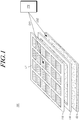
- FIG. 1 and FIG. 2 are diagrams schematically illustrating a configuration of a force touch display device.
- a force touch display device 100 may include a plurality of first electrodes E1 for sensing a touch or non-touch of a user and a touch position (touch coordinates), a second electrode E2 for sensing a touch force of the user, a display panel 110 in which the plurality of first electrodes E1 is embedded, a driving circuit 120 configured to drive the plurality of first electrodes E1 and the second electrode E2, and a gap structure unit 130 configured to maintain a gap between the plurality of first electrodes E1 and the second electrode E2.
- the force touch display device 100 may operate in a display mode for displaying an image or in a touch mode for sensing a touch (a touch or non-touch, a touch position, a touch force) of the user.
- touch display device 100 operates in the display mode, data lines and gate lines disposed in the display panel 110 are driven to display an image.
- the plurality of first electrodes E1 embedded in the display panel 110 is applied with a display driving voltage for image display. That is, the plurality of first electrodes E1 operates as an electrode for display driving in a display mode period.
- the first electrodes E1 are simultaneously used as common electrodes for applying a common voltage Vcom to a pixel and touch electrodes for touch recognition.
- a touch position (touch coordinates) of the user can be sensed or a touch force of the user can be sensed.
- touch sensing may include two kinds of touch sensing modes.
- a first touch sensing mode is a mode for sensing a touch position by applying a touch driving signal DS to a first electrode and measuring a self-capacitance of the first electrode, which is referred to, for convenience, as an in-cell touch mode or in-cell touch operation.
- the driving circuit 120 senses a touch position (touch coordinates) of the user by sequentially applying the first electrode driving signal DS1 to the plurality of first electrodes E1 and measuring a self-capacitance of the first electrodes during a predetermined in-cell touch driving period.
- the driving circuit 120 senses a touch force of the user by applying the first electrode driving signal DS1 to the plurality of first electrodes E1 and applying the second electrode driving signal to the second electrode E2.
- the force touch display device 100 senses a touch force of the user using a change in a gap between the plurality of first electrodes E1 and the second electrode E2 when the user's vertical load on the display panel 110 is generated.
- a capacitance between the both electrodes is measured, and if the user makes a touch, a gap between the both electrodes is changed at a touch position, which causes a change of the capacitance.
- the touch position can be determined by sensing the change of the capacitance.
- the gap structure unit 130 may be disposed between the plurality of first electrodes E1 and the second electrode E2.
- the gap structure unit 130 enables the gap between the plurality of first electrodes E1 and the second electrode E2 to be changed in size when the user makes a touch, and makes it possible to sense a touch position (touch coordinates) and a touch force of the user using the change in size of the gap.
- the touch display panel 110 of the touch display device 100 may include a first substrate 111 on which a thin film transistor (TFT) and the like are disposed and a second substrate 112 on which a color filter (CF) and the like are disposed.
- TFT thin film transistor
- CF color filter
- a driving chip 140 may be mounted on an edge area (non-active area (N/A)) of the first substrate 111 or may be bonded or connected to the non-active area N/A.
- the driving chip 140 may be a chip that implements the driving circuit 120 in whole or in part or may be a data driving chip. Otherwise, the driving chip 140 may be a display driving chip including the driving circuit 120 and a data driving circuit in whole or in part.
- the data driving chip may be denoted as D-IC, and within the data driving chip, a data driver configured to control display by applying a data signal to the data lines of the display panel and a touch driver configured to recognize a touch operation by applying a touch driving signal to the touch electrodes may be included.
- the touch driver is not necessarily included within the data driving chip and may also be provided separately from the data driver.
- a lower structure 131 may be positioned under the display panel 110, and the second electrode E2 may be positioned under or inside the lower structure 131.
- the lower structure 131 may be, for example, a back light unit of a liquid crystal display device.
- the second electrode E2 may be positioned under the back light unit. Therefore, the second electrode E2 may be disposed without interference in a light irradiation function of the back light unit.
- the gap structure unit 130 may be positioned under, inside, or beside the lower structure 131. Also, the second electrode E2 may be positioned under or inside the gap structure unit 130.
- a touch force sensing structure suitable for a design structure of the display panel 110 and the touch display device 100 can be implemented by variously designing a position of the second electrode E2 or a position of the gap structure unit 130. Details thereof will be described below with reference to FIG. 5 and FIG. 6 .
- the touch display device 100 will be described as a liquid crystal display device.
- FIG. 3 is a diagram illustrating a cross-section of the force touch display device 100
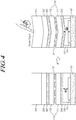
- FIG. 4 illustrates the situation where a gap between the first electrode E1 and the second electrode E2 is changed by the user's touch on the force touch display device 100.
- the display panel 110 of the touch display device 100 includes a first polarizing plate 310, the first substrate 111, the plurality of first electrodes E1, the second substrate 112, and a second polarizing plate 320.
- a bonding layer 330 and an upper cover 340 are positioned on the display panel 110.
- the touch display device 100 applies the first electrode driving signal DS1 to the plurality of first electrodes E1 in an in-cell touch operation period in which only the first electrodes are used during a touch mode.
- a change in size of a self-capacitance SC between a conductive pointer such as the user's finger and the plurality of first electrodes E1 is sensed to sense a touch position (touch coordinates) of the user.
- the touch display device 100 applies the first electrode driving signal DS1 to the plurality of first electrodes E1 and the second electrode driving signal DS2 to the second electrodes E2 in a force touch operation period for sensing a touch force of the user during the touch mode.
- the second electrode driving signal DS2 applied to the second electrode E2 may be a signal of a ground voltage.
- a change of a mutual capacitance MC caused by a change of a gap G between the plurality of first electrodes E1 and the second electrodes E2 is sensed to sense a touch force of the user.
- a touch position (touch coordinates) is sensed by sensing a change of the self-capacitance SC generated in the first electrodes when the user makes a touch
- a touch force is sensed by sensing a change of the mutual capacitance MC between the first electrodes and the second electrode.
- the gap G needs to be formed between the plurality of first electrodes E1 and the second electrodes E2 so as to make a change of the mutual capacitance MC between the first electrodes and the second electrode.
- the upper cover 340, the display panel 110, and the like are slightly bent downwards.
- a size of the gap G such as an air gap or dielectric gap, present between the plurality of first electrodes E1 and the second electrode E2 may be changed.
- G1 the gap G before the generation of the vertical load caused by the user's touch
- G2 the gap G after the generation of the vertical load caused by the user's touch
- the gap G between the plurality of first electrodes E1 and the second electrode E2 is decreased from G1 to G2 due to the generation of the vertical load caused by the user's touch, which results in a change of the mutual capacitance MC, and, thus, a touch force of the user can be sensed.
- the second electrode E2 for sensing a touch force of the user may be a component added to the touch display device 100 for touch force sensing, or a component already included in the touch display device 100 may be used as the second electrode E2.
- a back cover of the back light unit included in the liquid crystal display device may be used as the second electrode E2 to sense a touch force of the user.
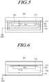
- FIG. 5 and FIG. 6 illustrate various configuration methods of a first electrode and a second electrode for force touch sensing in the force touch display device.
- the term "display device” is used to refer to a display device such as a display module including a liquid crystal module(LCM), an organic light emitting display module(OLED module) or another type of display module, which includes a display panel and a driver for driving the display panel as well as a concept including even a set electronic device or a set device such as a notebook computer, a television, a computer monitor, and a mobile electronic device such as a smartphone or an electronic pad, which are complete products including the display module.
- LCD liquid crystal module
- OLED module organic light emitting display module
- a display device including a display panel, a driver controlling a touch and image display on the display panel, and a support structure supporting the driver is referred to as “display module”, and a set electronic device as a complete product including the display module is referred to as “set device” or “display device”.
- a liquid crystal display panel 510, a back light unit 520 for providing back light thereto, and a cover bottom 530 as a support structure configured to a back surface of the back light unit may be referred to as "liquid crystal display module”, and a complete product further including a cover glass 540 configured to protect a front surface of the liquid crystal display panel and a mid-frame 550 configured to support the back of the liquid crystal display module and thus serving as a support structure for the entire set device may be referred to as "set device” or "display device”.
- the cover bottom 530 of display module is used as a second electrode for force touch.
- a first electrode 512 used as a common electrode and touch electrode is disposed within the liquid crystal display panel 510.
- the first electrode is used as a touch electrode during an in-cell touch operation and also used as a touch electrode corresponding to a second electrode during a force touch operation.
- the cover bottom 530 of the liquid crystal display module is used as a second electrode for force touch, and a ground signal which is the second electrode driving signal DS2 may be input into the cover bottom.
- a force touch is sensed in a state where the first electrode 512 disposed within the liquid crystal display panel is applied with the first electrode driving signal DS1 and the cover bottom 530 used as the second electrode is applied with the ground signal GND as the second electrode driving signal.
- a gap as a space for force touch sensing needs to be formed between the first electrode 512 and the cover bottom 530 serving as the second electrode.
- a space between the liquid crystal display panel 510 including the first electrode and the cover bottom 530 may be used as the gap.
- the gap needs to be variable due to a pressing force of the user. Therefore, the back light unit disposed as a fixed body between the first electrode and the second electrode cannot be used as a gap structure. Accordingly, a first air gap AG1 which is a variable gap needs to be formed between a back surface of the liquid crystal display panel 510 and the back light unit 520.
- the first electrode and the second electrode, i.e., the cover bottom, within the display panel are used and a change of a first capacitance C1 between the both electrodes caused by a change of the first air gap AG1 which is a variable gap between the back surface of the liquid crystal display panel 510 and the back light unit 520 is measured to sense a force touch.
- the force touch display device as illustrated in FIG. 5 may further include the cover glass 540 configured to protect the front surface of the liquid crystal display panel and the mid-frame 550 configured to support the back of the liquid crystal display module and thus serving as a support structure for the entire set device besides the above-described liquid crystal display module.
- the mid-frame 550 is irrelevant to force touch sensing.
- FIG. 6 is a cross-sectional view of another type of a force touch display device and illustrates an example where a separate cover bottom is not used.
- a cover bottom as a support structure for a back surface of a liquid crystal display module is not used, and a mid-frame as a back structure for a set device is disposed directly on a back surface of a back light unit.
- the mid-frame 550 functions as a second electrode and a second air gap AG2 is formed between the back light unit 520 and the mid-frame 550 and a size of the second air gap AG2 is changed during a touch operation of the user.
- a force touch can be recognized.
- a second capacitance C2 between the first electrode and the second electrode is changed depending on a change in size of the second air gap AG2.
- An input of a force touch can be recognized by measuring the change of the second capacitance C2.
- the cover bottom of the display module is used as a second electrode as illustrated in FIG. 5
- the cover bottom may be bent or warped in use. Such solution is more stable, since two structures are used
- the first air gap AG1 is requisitely formed between the liquid crystal display panel 510 and the back light unit 520, which might increase the overall thickness of the display device.
- the capacity can not be changed easily due to the cover bottom 530 and the mid frame 550.
- the structure in which the mid-frame 550 of the set device is used as a second electrode as illustrated in FIG. 6 cannot be applied to a display device with a cover bottom.
- a display module is manufactured separately and then delivered to a complete product manufacturer, and, thus, a display module manufacturer needs to manufacture and supply a display module without a cover bottom in order to apply the force touch display device as illustrated in FIG. 6 .
- the manufactured display module without a cover bottom is likely to be damaged during delivery and thus has not been widely used. Therefore, the force touch display device as illustrated in FIG. 6 cannot be widely applied.
- a cover bottom-cut force touch display device in which a part of a cover bottom is removed as illustrated in FIG. 7 may be suggested.
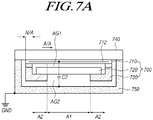
- FIG. 7 illustrates a cross-sectional structure of a cover bottom-cut force touch display device to which the present exemplary embodiment can be applied.
- FIG. 8 is a plan view illustrating the layout of a first electrode of the force touch display device according to the present exemplary embodiment.
- the cover bottom-cut force touch display device has the advantages of the structures illustrated in FIG. 5 and FIG. 6 .
- a display module includes a cover bottom of which a central area is removed and which is present only on an edge area of the display module, and a mid-frame of a set device is used as a second electrode.
- the force touch display apparatus includes a display module 700 including a display panel 710 including a first electrode 712 therein, a back light unit 720 configured to supply light to the display panel, and a cut cover bottom 730 of which a central area is removed and which supports only an edge area of the back light unit, a cover glass 740 disposed on a front side of the display panel, and a mid-frame 750 connected to the cover glass and configured as a back structure for the entire display device (set device).
- a display module 700 including a display panel 710 including a first electrode 712 therein, a back light unit 720 configured to supply light to the display panel, and a cut cover bottom 730 of which a central area is removed and which supports only an edge area of the back light unit, a cover glass 740 disposed on a front side of the display panel, and a mid-frame 750 connected to the cover glass and configured as a back structure for the entire display device (set device).
- the cut cover bottom 730 is a bottom portion which has central portion which has been removed. Thus, a central portion of the cut cover bottom 730 is open.
- the mid-frame 750 serves as a second electrode and a ground signal is applied thereto.
- a second air gap AG2 as a space between a back surface of the back light unit and the mid-frame is defined.
- the first electrode 712 is applied with a first electrode driving signal and the mid-frame 750 as the second electrode is applied with a ground signal as a second electrode driving signal.
- a size of the second air gap AG2 is changed at that position. Therefore, a second capacitance C2 between the first electrode and the second electrode is changed. By measuring the amount of change of the second capacitance C2, a force touch position can be sensed.
- the force touch display device as illustrated in FIG. 7 can overcome the disadvantages of the structures as illustrated in FIG. 5 and FIG. 6 .
- the cover bottom is overlapped with a part of an active area A/A of the display panel and the overlapped area has different force touch performance from a central area A1 where the cover bottom is removed.
- the first electrode of the force touch display device includes the central area A1 where the first electrode is not overlapped with the cover bottom and an edge area A2 where the first electrode is overlapped with the cover bottom as illustrated in FIG. 8 .
- the cut cover bottom may be only partially overlapped with touch electrodes (i.e., outermost touch electrode block) on a line disposed on the outermost edge or may be entirely overlapped with the touch electrodes (i.e., outermost touch electrode block) on the line disposed on the outermost edge.
- a force touch can be sensed on the central area A1 where the cover bottom is removed.
- a part of the edge area A1 where the cut cover bottom remains is overlapped with a part of the active area A/A of the display device, and in this overlapped area, the cover bottom formed of metal is present between the mid-frame 750 as the second electrode and the first electrode, and, thus, a desired force touch performance cannot be secured.
- the force touch display device has the structure as illustrated in FIG. 7 .
- a data driver or a touch driver uses one selected from the mid-frame 750 and the cut cover bottom 730 as the second electrode in order to sense a force touch on the central area A1 and the edge area A2 of the first electrode.
- FIG. 9 illustrates the force touch display device according to the present exemplary embodiment in which a touch control unit switches a second electrode when the touch control unit senses a force touch on the central area and the edge area.
- the force touch display device includes the display panel 710 including the first electrode 712 for touch sensing, the cut cover bottom disposed to cover a back surface of the edge area of the display panel and serving as a first support part, the mid-frame 750 disposed on a back side of the cut cover bottom and serving as a second support part covering the entire back surface of the display panel, and a touch driver configured to sense a touch input into the display panel.
- a touch driver 780 may be implemented as being included in a data driving circuit D-IC configured to control image output of the display panel. Therefore, in the present specification, for convenience, the touch driver is illustrated as a data driving circuit but is not limited thereto.
- the touch driver 780 performs a force touch operation for recognizing the user's touch pressure applied to the display panel as a force touch.
- This force touch operation functions to sense the user's touch pressure applied to the display panel by applying a first electrode driving signal to the first electrode, selecting one of the cut cover bottom 730 and the mid-frame 750 as the second electrode, and then applying a second electrode driving signal to the selected second electrode.
- the cut cover bottom 730 as illustrated in FIG. 7 is configured as the first support part for the display module and the mid-frame 750 on its back side is configured as the second support part for the entire display device (set device), and in case of a force touch, one of the cut cover bottom and the mid-frame is selected as the second electrode. That is, according to the present exemplary embodiment, the cut cover bottom 730 can be used as the second electrode for force touch besides the mid-frame 750.
- the second electrode driving signal may be a ground signal
- the touch driver may determine an input of a force touch by applying the ground signal as the second electrode driving signal to the selected second electrode and then measuring a change of a capacitance between the first electrode and the second electrode.
- the touch driver selects the mid-frame 750 as the second electrode. If a touch pressure is sensed on the edge area A2 of the first electrode which is partially overlapped with the cut cover bottom, the touch driver selects the cut cover bottom 730 as the second electrode.
- the touch driver may drive touch input sensing on the central area A1 and touch input sensing on the edge area A2 in a time-division manner.
- the touch driver 780 in order to sense a force touch on the edge area A2 of the first electrode which is partially overlapped with the cut cover bottom, applies the ground signal (second electrode driving signal) to the cut cover bottom 730 and then measures a change of a first capacitance C1 formed between the first electrode 712 applied with the first electrode driving signal and the second electrode and thus senses a force touch.
- the ground signal second electrode driving signal
- the touch driver 780 applies the ground signal (second electrode driving signal) to the mid-frame 750 as a back support structure for the set device and then measures a change of a second capacitance C2 formed between the first electrode 712 applied with the first electrode driving signal and the second electrode and thus senses a force touch.
- a force touch can be sensed on the edge area A2 where the cut cover bottom is overlapped with the active area. Therefore, force touch performance on the outermost touch electrode block can be improved in both of a case where the cut cover bottom is only partially overlapped with touch electrodes (i.e., outermost touch electrode block) on a line disposed on the outermost edge and a case where the cut cover bottom is entirely overlapped with the touch electrodes (i.e., outermost touch electrode block) on the line disposed on the outermost edge.
- the other one which is not selected as the second electrode from among the cut cover bottom and the mid-frame needs to be continuously floated and maintained in a high-impedance state Hi-Z.
- the cover bottom or the mid-frame which is not selected as the second electrode is maintained at a constant potential, a constant and unnecessary capacitance may be generated between the non-selected one and the first electrode, and the unnecessary capacitance may be added to the second capacitance C2 measured from the first electrode during a normal force touch operation and thus may cause a decrease in measurement precision.
- a size of the first air gap AG1 for measurement of the first capacitance C1 is smaller than that of the second air gap AG2 in the central area.
- a magnitude of the first capacitance C1 for force touch sensing is relatively low. Therefore, in this case, if the mid-frame which is not selected as the second electrode is not floated and an unnecessary capacitance is generated between the first electrode and the mid-frame and then added to the first capacitance, force touch performance may be further degraded on the edge area A2 than on the central area A1.
- the other one which is not selected as the second electrode from among the cut cover bottom and the mid-frame needs to be continuously floated and maintained in the high-impedance state Hi-Z.
- the force touch display device may further include the back light unit 720 disposed between the display panel 710 and the cut cover bottom 730 and configured to supply light to the display panel.
- the first air gap AG1 needs to be formed between the back light unit 720 and the display panel 710.
- an adhesive member 714 having a uniform thickness may be disposed between an edge of the display panel 710 and the cutting cover bottom 730 so as to bond the both members and form the first air gap AG1 between the back light unit and the display.
- a touch input position can be determined.
- the second air gap AG2 is formed between the back light unit 720 and the mid-frame 750 besides the above-described first air gap.
- a variable space between the both electrodes in the central area A1 may be the sum of the first air gap and the second air gap, and a variable space between the both electrodes in the edge area A2 is the first air gap.
- the amount of change of the second capacitance C2 in the central area A1 is greater than the amount of change of the first capacitance C1 in the edge area A2.
- the number of first levels for touch pressure sensing on the central area A1 is set to be greater than the number of second levels for touch pressure sensing on the edge area A2.
- a first force touch sensing signal (data) indicating a change of the second capacitance for force touch sensing on the central area A1 has 8 bits and may have a total of 256 first levels
- a second force touch sensing data on the edge area A2 has 2 bits and may have a total of 4 second levels.
- a force touch sensitivity or resolution on the central area A1 is set to be higher than a force touch sensitivity or resolution on the edge area A2, and, thus, a force touch can be sensed precisely on the central area and can also be sensed on the edge area which is overlapped with the cover bottom and on which a force touch cannot be sensed according to the prior art. Therefore, a force touch sensing area is extended.
- the touch driver 780 may drive force touch input sensing on the central area A1 and touch input sensing on the edge area A2 in a time-division manner.
- a force touch operation can be readily performed on the entire display panel.
- the cut cover bottom 730 is not limited to the term itself and may be used as other expressions such as a plate bottom, a base frame, a metal frame, a metal chassis, a chassis base, and an m-chassis. Further, the cut cover bottom 730 should be interpreted to include all types of frames or plate-shaped structures supporting a back side of an edge of at least one of the display panel and the back light unit.
- the cut cover bottom 730 used in the present exemplary embodiment is not disposed in the central area of the display device but supports only the edge of the display device.
- the mid-frame 750 is not limited to the term itself and should be interpreted to include all types of support structures supporting a hindmost side of the set device as a complete product including the display panel. Further, the mid-frame 750 can be substituted by other terms such as a back cover, and a set cover.
- the display panel 710 used in the present exemplary embodiment is a liquid crystal display panel
- the display panel 710 may include a plurality gate lines and data lines, pixels defined on intersections therebetween, an array substrate including a thin film transistor which is a switching element for adjusting light transmittance in each pixel, an upper substrate including a color filter and/or a black matrix, and a liquid crystal material layer formed therebetween.
- the present exemplary embodiment is not necessary limited to a liquid crystal display device, but can be applied to all types of display systems including a first electrode for touch sensing therein and capable of sensing a force touch caused by a change of a gap between the first electrode and a second electrode separate from the first electrode.
- the first electrode 712 functions as a common electrode configured to supply a common voltage to pixels included in the display panel.
- the single first electrode may be disposed so as to cover a plurality of pixels.
- FIG. 10 illustrates an internal configuration of the touch control unit (or data driver) for switching the second electrode and a structure for supplying a ground signal to the cover bottom and the mid-frame in the force touch display device according to the present exemplary embodiment.
- the touch driver 780 may be included in a data driving circuit D-IC, and the data driving circuit D-IC may include a first ground output terminal P1, a second ground output terminal P2, and a switching unit SW configured to switch the output of a ground signal to the first and second ground output terminals.
- the data driving circuit D-IC may further include a flexible printed circuit (FPC) 790 connected to the data driving circuit D-IC so as to connect an external set PCB and the data driving circuit.
- FPC flexible printed circuit
- the FPC 790 may include a first ground signal line GL1 extended from the first ground output terminal of the data driving circuit D-IC and a second ground signal line GL2 extended from the second ground output terminal.
- the first ground signal line GL1 may be electrically connected to the cut cover bottom 730 and the second ground signal line GL2 may be electrically connected to the mid-frame 750.
- a custom pin within the data driving circuit D-IC includes the first ground output terminal P1 and the second ground output terminal P2, and the two ground signal lines GL1 and GL2 are further disposed in the FPC in addition to other ground signal lines and then connected to the cut cover bottom 730 and the mid frame 750, respectively.
- the touch driver uses the switching unit SW to control the output of a ground signal to the first ground output terminal P1 and the second ground output terminal P2 in a time-division manner during a force touch sensing operation on the central area A1 and the edge area A2.
- a part of the first ground signal line GL1 formed in the FPC 790 may be opened and then attached to the cut cover bottom 730 using a conductive tape or the like so as to be electrically connected thereto.
- a connector or the like at an end of the second ground signal line GL2 formed in the FPC 790 may be attached to the mid-frame 750.
- the second ground signal line may be electrically connected to the mid-frame.
- the first electrodes as a touch electrodes included in a display panel include a plurality of touch electrode block groups disposed in the display panel, and each of the touch electrode block groups may include a plurality of touch electrode blocks.
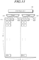
- the first electrode has a structure in which a first touch electrode block group including k number of first touch electrode blocks disposed on the left (first side) of the display panel and a second touch electrode block group including k number of second touch electrode blocks on the right (second side) of the display panel are symmetrically disposed, and each of the first touch electrode block and the second touch electrode block may include a column of m number of touch electrodes.
- each touch block includes a total of 32 touch electrodes disposed in a longitudinal direction.
- Each touch electrode and touch electrode block is not necessarily identical to each other in size and number.
- a touch electrode block disposed on an edge of the display panel may include a smaller number of blocks or touch electrodes than the other touch electrode blocks, and, thus, it is possible to maintain a uniform touch sensitivity.
- the force touch display device further includes touch multiplexers (T-MUX) 1190 and 1190' configured to switch the application of a touch driving signal to a plurality of touch electrodes included in each of the first touch electrode blocks and the second touch electrode blocks.
- the T-MUX includes a first T-MUX 1190 in charge of the first touch electrode blocks on the left and a second T-MUX 1190' in charge of the second touch electrode blocks on the right.
- the first T-MUX 1190 sequentially supplies a first electrode driving signal to a total of 9 first touch electrode blocks to perform touch sensing
- the second T-MUX 1190' sequentially supplies the first electrode driving signal to a total of 9 second touch electrode blocks to perform touch sensing.
- first T-MUX 1190 and the second T-MUX 1190' may perform their operations in a symmetrical manner.
- the second T-MUX also applies the first electrode driving signal to an ith second touch electrode block.
- the touch display device may perform both a first touch operation of sensing a touch input using only the first electrodes and a second touch operation of sensing a touch input using the first electrodes and the second electrode.
- the first touch operation using only the first electrodes within the display panel is expressed as "in-cell touch” and the second touch operation using all the first electrodes and the second electrode is expressed as "force touch”, but are not limited to these expressions.
- a touch driver applies the first electrode driving signal only to the first electrodes and measures a self-capacitance generated in the first electrodes to sense a touch input during an in-cell touch operation period.
- the touch driver applies the first electrode driving signal to the first electrodes and applies a second electrode driving signal to the second electrode which is one of a cut cover bottom or a mid-frame, and then measures a mutual capacitance between the first electrodes and the second electrode to sense a touch pressure.
- the in-cell touch mode (first touch operation) and the force touch mode (second touch operation) may be driven in a time-division manner.
- the in in-cell touch mode (first touch operation) and the force touch mode (second touch operation) need not necessarily operate in a time division manner, and the in in-cell touch mode (first touch operation) and the force touch mode (second touch operation) may respectively operate alone.
- the first and second touch operation or modes may be a first force touch operation for the central area A1 where the cover bottom is removed and a second force touch operation for the edge area A2 where a part of the first electrode and the cut cover bottom are partially overlapped,
- FIG. 12 illustrates an example of a time-division driving method of an in-cell touch mode, a display mode, and a force touch mode in the force touch display device according to the present exemplary embodiment.
- a display operation mode for displaying an image on pixels and a touch operation mode are repeatedly performed in a time-division manner.
- an in-cell touch mode is performed to first to third touch electrode blocks from among the touch electrode blocks illustrated in FIG. 11 and then a first display operation mode D1 is performed thereto.
- in-cell touch sensing is performed to fourth to sixth touch electrode blocks and then a second display operation mode D2 is performed thereto.
- in-cell touch sensing is performed to seventh to ninth touch electrode blocks.
- an operation including sequentially applying the first electrode driving signal only to first to third first touch electrode blocks and first to third second touch electrode blocks under the control of the T-MUX during the first touch operation period T1 and sequentially applying the first electrode driving signal only to fourth to sixth first touch electrode blocks and fourth to sixth second touch electrode blocks under the control of the T-MUX during the second touch operation period T2 is repeated to perform in-cell touch sensing.
- a fourth touch operation period T4 force touch sensing is performed. That is, during the fourth touch operation period T4, the first electrode driving signal is sequentially applied to all of the first electrodes. At the same time, the ground signal is applied to the second electrode. Then, a capacitance between the both electrodes is measured to sense a force touch.
- a touch position is identified via in-cell touch sensing, and then the touch position is confirmed via force touch sensing.
- touch sensing is performed twice to a single display panel, and, thus, touch recognition can be further improved.
- a touch sensing frequency may be 120 Hz, but is not limited thereto.
- FIG. 13 illustrates a force touch operation via a shift of the second electrode according to the present exemplary embodiment, and illustrates an example of data formats or numbers of levels of a touch sensing signal on the central area A1 and a touch sensing signal on the edge area A2.
- FIG. 13 illustrates a detailed flow of force touch sensing during the fourth touch operation period T4 in the time-division touch sensing illustrated in FIG. 12 .
- a scan start signal for the central area A1 which is not overlapped with the cover bottom is applied (S1310), and then the second capacitance C2 between the first electrode disposed in the central area A1 and the mid-frame (second electrode) is received as a touch signal and a touch position is sensed (S1320).
- the first electrode driving signal is applied to the first electrodes in the entire area including the central area A1 and the edge area A2 and the second electrode driving signal GND is applied to the mid-frame selected as the second electrode, and then a capacitance between the both electrodes is measured.
- the touch driver ignores a capacitance value measured from the edge area A2 but obtains only a capacitance value measured from the central area A1.
- the first electrode driving signal is applied to the first electrodes in the entire area including the central area A1 and the edge area A2 and the second electrode driving signal GND is applied to the cut cover bottom selected as the second electrode, and then a capacitance between the both electrodes is measured.
- the second electrode driving signal GND is applied to the cut cover bottom selected as the second electrode, and then a capacitance between the both electrodes is measured.
- there is no second electrode corresponding to the first electrode in the central area A1 as illustrated in FIG. 9 and, thus, a capacitance cannot be measured from the central area. Therefore, only a capacitance value measured from the edge area A2 is obtained.
- the amount of change of the second capacitance C2 measured from the central area A1 is greater than the amount of change of the first capacitance C1 measured from the edge area A2.
- the edge area A2 has a relatively small first air gap AG1 and the central area A1 has a large second air gap AG2, and, thus, if the same touch pressure is applied, a change of the gap and a resultant change of the capacitance are greater in the central area.
- a force touch sensitivity is lower in the edge area A2 than in the central area A1. That is, the number of levels to identify the degree of force touch in the central area A1 is greater than that of the edge area A2.
- the number of first levels for touch sensing on the central area A1 is set to be greater than the number of second levels for touch sensing on the edge area.
- a force touch signal measured from the central area A1 is data with 8 bits and may have a total of 256 first levels
- a force touch signal measured from the edge area A2 is data with 2 bits and may have a total of 4 second levels.
- the first number of levels for sensing a touch input on the first area of the display panel may be different from the second number of levels for sensing a touch input on the second area of the display panel.
- the first number of levels for sensing a touch input on the first electrodes disposed on the central area of the display panel may be greater than the second number of levels for sensing a touch input on the first electrodes disposed on the edge area of the display panel.
- the entire area of the display device can secure uniform touch performance in a force touch method in which a partial area of a cover bottom configured to support a back surface of a display panel is cut.
- the entire area of the display device can secure uniform touch performance by selectively applying a ground (GND) signal to a mid-frame configured to support a back surface of a set device and a cut cover bottom depending on a force touch sensing area.
- GND ground
- a ground signal is applied to the cover bottom.
- the number of second levels for force touch sensing on the edge area of the display panel is set to be smaller than the number of first levels for force touch sensing on a central area of the display panel.
Landscapes
- Engineering & Computer Science (AREA)
- General Engineering & Computer Science (AREA)
- Physics & Mathematics (AREA)
- Theoretical Computer Science (AREA)
- General Physics & Mathematics (AREA)
- Human Computer Interaction (AREA)
- Nonlinear Science (AREA)
- Chemical & Material Sciences (AREA)
- Crystallography & Structural Chemistry (AREA)
- Mathematical Physics (AREA)
- Optics & Photonics (AREA)
- Liquid Crystal (AREA)
- Devices For Indicating Variable Information By Combining Individual Elements (AREA)
Abstract
Description
- This application claims priority from Korean Patent Application No.
10-2016-0125600, filed on September 29, 2016 - The present invention relates to a touch display device.
- With progress of the information-oriented society, various types of demands for display devices for displaying an image are increasing. Various types of display devices such as a liquid crystal display device, a plasma display device, and an organic light emitting diode display device have been used.
- From among these display devices, a mobile device such as a smartphone or a tablet PC and a medium and large device such as a smart television provide a touch input process according to user's convenience and device characteristics.
- Such display devices capable of performing a touch input process are being developed so as to provide more functions, and users' demands are also getting various.
- However, the currently-applied touch input process includes sensing only a user's touch position (touch coordinates) and performing an input process relevant to the sensed touch position, and, thus, has limits under the current circumstances in which it is necessary to provide various kinds of functions in various forms and satisfy the users' demands.
- An aspect of the present invention provides a touch display device capable of sensing a touch position by sensing a touch force corresponding to a pressing force on a screen when a user touches the screen.
- Another aspect of the present invention provides a touch display device in which a touch force corresponding to a pressing force on a screen when a user touches the screen can be uniformly sensed at each position of a display panel.
- Yet another aspect of the present invention provides a back light unit having a structure which enables a reduction in thickness of touch display device capable of sensing a touch force and also provides a touch display device including the same.
- Still another aspect of the present invention provides a touch display device of which the entire area can secure uniform touch performance in a force touch method in which a partial area of a cover bottom configured to support a back surface of a display panel is cut.
- Still another aspect of the present invention provides a cover bottom-cut force touch display device of which the entire area can secure uniform touch performance by selectively applying a ground (GND) signal to a mid-frame configured to support a back surface of a set device and a cut cover bottom depending on a force touch sensing position.
- The object is solved by a force touch display device comprising: display panel; a plurality of first electrodes disposed within the display panel, a second electrode for sensing a touch force of the user, wherein a gap is formed between the first electrode and the second electrode, which is variable when a touch force of the user is applied.
- Preferably, the display panel comprises a first substrate, the plurality of first electrodes and a second substrate.
- According to an aspect of the present invention, there is provided a force touch display device including a cut cover bottom (first support part) configured to support only an edge of a display panel including a first electrode for touch sensing and a mid-frame (second support part) configured to cover the entire back surface of the display panel. In the force touch display device, a touch driver is configured to select one of the cut cover bottom and the mid-frame as a second electrode depending on a force touch sensing position and apply a second electrode driving signal (GND).
- Preferably, the gap is formed by a gap structure unit disposed between the plurality of first electrodes and the second electrode.
- Preferably, a lower structure is disposed between the display panel and the second electrodes.
- Preferably, wherein a part of the cover bottom is removed or cut.
- Preferably, the cover bottom being cut, is called hereinafter cut cover bottom, or the mid-frame are used as a second electrode.
- More specifically, if the touch driver senses a touch pressure on a central area A1 of the first electrode which is not overlapped with the cut cover bottom, the touch driver selects the mid-frame as the second electrode, and if the touch driver senses a touch pressure on an edge area A2 of the first electrode which is partially overlapped with the cut cover bottom, the touch driver selects the cut cover bottom as the second electrode and then applies the ground signal thereto.
- To this end, the touch driver may be included in a data driving circuit D-IC, and the data driving circuit may include a first ground output terminal, a second ground output terminal, and a switching unit configured to switch the output of a ground signal to the first and second ground output terminals.
- Also, the force touch display device may further include a flexible printed circuit (FPC) connected to the data driving circuit and including a first ground signal line extended from the first ground output terminal and a second ground signal line extended from the second ground output terminal. The first ground signal line and the second ground signal line of the FPC may be electrically connected to the cut cover bottom and the mid-frame, respectively.
- Meanwhile, the touch driver may set the number of first levels for touch pressure sensing on the central area A1 to be greater than the number of second levels for touch pressure sensing on the edge area A2, and drive touch input sensing on the central area and touch input sensing on the edge area in a time-division manner.
- Further, the touch driver may sense a first touch input by measuring a self-capacitance generated in the first electrode in response to the first electrode driving signal applied to the first electrode in a first touch operation (in-cell touch mode) period and sense a user's force touch input applied to the display panel by applying the first electrode driving signal to the first electrode and applying the second electrode driving signal to the second electrode selected from the cut cover bottom and the mid-frame in a second touch operation (force touch mode) period.
- According to the present exemplary embodiments, the entire area of a display device can secure uniform touch performance in a force touch method in which a partial area of a cover bottom configured to support a back surface of a display panel is cut.
- More specifically, the entire area of a cover bottom-cut force touch display device can secure uniform touch performance by selectively applying a ground (GND) signal to a mid-frame configured to support a back surface of a set device and a cut cover bottom depending on a position of applying a touch driving signal.
- The object is also solved by a touch display device comprising: a display panel including a first area and a second area; a touch driver configured to sense a touch input on the display panel; wherein a first number of levels for sensing the touch input on the first area of the display panel is different from the second number of levels for sensing the touch input on the second area of the display panel.
- Particularly, in case of sensing a force touch on an edge area where a cut cover bottom is present, a ground signal is applied to the cover bottom. Herein, the number of second levels for force touch sensing on the edge area of the display panel is set to be smaller than the number of first levels for force touch sensing on a central area of the display panel. Thus, force touch performance of the entire display device can be improved.
- The above and other aspects, features and other advantages of the present invention will be more clearly understood from the following detailed description taken in conjunction with the accompanying drawings, in which:
-
FIG. 1 andFIG. 2 are diagrams schematically illustrating a configuration of a force touch display device; -
FIG. 3 is a diagram illustrating a cross-section of the force touch display device; -
FIG. 4 is a diagram illustrating the situation where a gap is changed in the force touch display device and the principle of sensing a force touch accordingly. -
FIG. 5 and FIG. 6 illustrate various configuration methods of a first electrode and a second electrode for force touch sensing in the force touch display device; -
FIG. 7 illustrates a cross-sectional structure of a cover bottom-cut force touch display device to which the present exemplary embodiment can be applied; -
FIG. 8 is a plan view illustrating the layout of a first electrode of the force touch display device according to the present exemplary embodiment in which the first electrode includes a central area which is not overlapped with a cover bottom and an edge area which is overlapped with the cover bottom; -
FIG. 9 illustrates the force touch display device according to the present exemplary embodiment in which a touch control unit switches a second electrode when the touch control unit senses a force touch on the central area and the edge area; -
FIG. 10 illustrates an internal configuration of the touch control unit (or data driver) for switching the second electrode and a structure for supplying a ground signal to the cover bottom and the mid-frame in the force touch display device according to the present exemplary embodiment; -
FIG. 11 illustrates an example of the layout of the first electrodes of the force touch display device according to the present exemplary embodiment and illustrates a structure in which two touch electrode groups are symmetrically disposed and each of the touch electrode groups includes k (k=9) number of touch electrode blocks; -
FIG. 12 illustrates an example of a time-division driving method of an in-cell touch mode, a display mode, and a force touch mode in the force touch display device according to the present exemplary embodiment; and -
FIG. 13 illustrates a force touch operation via a shift of the second electrode according to the present exemplary embodiment, and illustrates an example of data formats or numbers of levels of a touch sensing signal on a central area A1 and a touch sensing signal on an edge area A2. - Hereinafter, some embodiments of the present invention will be described in detail with reference to the accompanying drawings. When reference numerals refer to components of each drawing, although the same components are illustrated in different drawings, the same components are referred to by the same reference numerals as possible. Further, if it is considered that description of related known configuration or function may cloud the gist of the present invention, the description thereof will be omitted.
- Further, in describing components of the present invention, terms such as first, second, A, B, (a), and (b) can be used. These terms are used only to differentiate the components from other components. Therefore, the nature, order, sequence, or number of the corresponding components is not limited by these terms. It is to be understood that when one element is referred to as being "connected to" or "coupled to" another element, it may be directly connected to or directly coupled to another element, connected to or coupled to another element, having still another element "intervening" therebetween, or "connected to" or "coupled to" another element via still another element.
-
FIG. 1 andFIG. 2 are diagrams schematically illustrating a configuration of a force touch display device. - Referring to
FIG. 1 , a forcetouch display device 100 may include a plurality of first electrodes E1 for sensing a touch or non-touch of a user and a touch position (touch coordinates), a second electrode E2 for sensing a touch force of the user, adisplay panel 110 in which the plurality of first electrodes E1 is embedded, adriving circuit 120 configured to drive the plurality of first electrodes E1 and the second electrode E2, and agap structure unit 130 configured to maintain a gap between the plurality of first electrodes E1 and the second electrode E2. - The force
touch display device 100 may operate in a display mode for displaying an image or in a touch mode for sensing a touch (a touch or non-touch, a touch position, a touch force) of the user. - If the
touch display device 100 operates in the display mode, data lines and gate lines disposed in thedisplay panel 110 are driven to display an image. - In this case, the plurality of first electrodes E1 embedded in the
display panel 110 is applied with a display driving voltage for image display. That is, the plurality of first electrodes E1 operates as an electrode for display driving in a display mode period. - Specifically, the first electrodes E1 are simultaneously used as common electrodes for applying a common voltage Vcom to a pixel and touch electrodes for touch recognition.
- If the
touch display device 100 operates in the touch mode, a touch position (touch coordinates) of the user can be sensed or a touch force of the user can be sensed. - That is, touch sensing may include two kinds of touch sensing modes. A first touch sensing mode is a mode for sensing a touch position by applying a touch driving signal DS to a first electrode and measuring a self-capacitance of the first electrode, which is referred to, for convenience, as an in-cell touch mode or in-cell touch operation.
- A second touch sensing mode is a mode for recognizing a touch position by applying a first electrode driving signal DS1 and a second electrode driving signal DS2 to a first electrode and a second electrode, respectively, and measuring a change of a capacitance between the both electrodes when a gap between the first electrode and the second electrode is changed due to a touch operation, which is referred to, for convenience, as a force touch mode or force touch operation.
- That is, in the in-cell touch mode, the driving
circuit 120 senses a touch position (touch coordinates) of the user by sequentially applying the first electrode driving signal DS1 to the plurality of first electrodes E1 and measuring a self-capacitance of the first electrodes during a predetermined in-cell touch driving period. - Further, during a predetermined force touch driving period, the driving
circuit 120 senses a touch force of the user by applying the first electrode driving signal DS1 to the plurality of first electrodes E1 and applying the second electrode driving signal to the second electrode E2. - The force
touch display device 100 senses a touch force of the user using a change in a gap between the plurality of first electrodes E1 and the second electrode E2 when the user's vertical load on thedisplay panel 110 is generated. - That is, in a state where different driving signals DS1 and DS2 are respectively applied to the first electrode and the second electrode, a capacitance between the both electrodes is measured, and if the user makes a touch, a gap between the both electrodes is changed at a touch position, which causes a change of the capacitance. The touch position can be determined by sensing the change of the capacitance.
- Therefore, a gap needs to be present between the plurality of first electrodes E1 embedded in the
display panel 110 and the second electrode E2 positioned outside thedisplay panel 110. In order to maintain the gap, thegap structure unit 130 may be disposed between the plurality of first electrodes E1 and the second electrode E2. - That is, the
gap structure unit 130 enables the gap between the plurality of first electrodes E1 and the second electrode E2 to be changed in size when the user makes a touch, and makes it possible to sense a touch position (touch coordinates) and a touch force of the user using the change in size of the gap. - Hereinafter, the structure of the force
touch display device 100 to which the present exemplary embodiment can be applied will be described in more detail with reference toFIG. 2 . - Referring to
FIG. 2 , thetouch display panel 110 of thetouch display device 100 according to the present exemplary embodiments may include afirst substrate 111 on which a thin film transistor (TFT) and the like are disposed and asecond substrate 112 on which a color filter (CF) and the like are disposed. - Further, a
driving chip 140 may be mounted on an edge area (non-active area (N/A)) of thefirst substrate 111 or may be bonded or connected to the non-active area N/A. - Herein, the
driving chip 140 may be a chip that implements the drivingcircuit 120 in whole or in part or may be a data driving chip. Otherwise, thedriving chip 140 may be a display driving chip including the drivingcircuit 120 and a data driving circuit in whole or in part. - The data driving chip may be denoted as D-IC, and within the data driving chip, a data driver configured to control display by applying a data signal to the data lines of the display panel and a touch driver configured to recognize a touch operation by applying a touch driving signal to the touch electrodes may be included.
- However, the touch driver is not necessarily included within the data driving chip and may also be provided separately from the data driver.
- A
lower structure 131 may be positioned under thedisplay panel 110, and the second electrode E2 may be positioned under or inside thelower structure 131. - The
lower structure 131 may be, for example, a back light unit of a liquid crystal display device. - In this case, the second electrode E2 may be positioned under the back light unit. Therefore, the second electrode E2 may be disposed without interference in a light irradiation function of the back light unit.
- The
gap structure unit 130 may be positioned under, inside, or beside thelower structure 131. Also, the second electrode E2 may be positioned under or inside thegap structure unit 130. - As described above, a touch force sensing structure suitable for a design structure of the
display panel 110 and thetouch display device 100 can be implemented by variously designing a position of the second electrode E2 or a position of thegap structure unit 130. Details thereof will be described below with reference toFIG. 5 and FIG. 6 . - Hereinafter, a method of sensing a touch position (touch coordinates) and a touch force of the user by the force
touch display device 100 will be described with reference toFIG. 3 andFIG. 4 . For convenience in explanation, thetouch display device 100 according to the present exemplary embodiments will be described as a liquid crystal display device. -
FIG. 3 is a diagram illustrating a cross-section of the forcetouch display device 100, andFIG. 4 illustrates the situation where a gap between the first electrode E1 and the second electrode E2 is changed by the user's touch on the forcetouch display device 100. - Referring to
FIG. 3 , thedisplay panel 110 of thetouch display device 100 includes a firstpolarizing plate 310, thefirst substrate 111, the plurality of first electrodes E1, thesecond substrate 112, and a secondpolarizing plate 320. - Further, a
bonding layer 330 and anupper cover 340 are positioned on thedisplay panel 110. - The
touch display device 100 applies the first electrode driving signal DS1 to the plurality of first electrodes E1 in an in-cell touch operation period in which only the first electrodes are used during a touch mode. - Further, when the user makes a touch, a change in size of a self-capacitance SC between a conductive pointer such as the user's finger and the plurality of first electrodes E1 is sensed to sense a touch position (touch coordinates) of the user.
- The
touch display device 100 applies the first electrode driving signal DS1 to the plurality of first electrodes E1 and the second electrode driving signal DS2 to the second electrodes E2 in a force touch operation period for sensing a touch force of the user during the touch mode. - In this case, the second electrode driving signal DS2 applied to the second electrode E2 may be a signal of a ground voltage.
- Further, when a vertical load is generated due to the touch of the user, a change of a mutual capacitance MC caused by a change of a gap G between the plurality of first electrodes E1 and the second electrodes E2 is sensed to sense a touch force of the user.
- That is, during an in-cell touch operation, a touch position (touch coordinates) is sensed by sensing a change of the self-capacitance SC generated in the first electrodes when the user makes a touch, and during a separate force touch operation, a touch force is sensed by sensing a change of the mutual capacitance MC between the first electrodes and the second electrode.
- In order to perform the force touch operation, the gap G needs to be formed between the plurality of first electrodes E1 and the second electrodes E2 so as to make a change of the mutual capacitance MC between the first electrodes and the second electrode.
- Referring to
FIG. 4 , if a vertical load is generated due to the user's touch, theupper cover 340, thedisplay panel 110, and the like, are slightly bent downwards. - Therefore, a size of the gap G, such as an air gap or dielectric gap, present between the plurality of first electrodes E1 and the second electrode E2 may be changed.
- According to an example as illustrated in
FIG. 4 , if the gap G before the generation of the vertical load caused by the user's touch is denoted by G1 and the gap G after the generation of the vertical load caused by the user's touch is denoted by G2, G2 is smaller than G1 due to the vertical load. - As such, the gap G between the plurality of first electrodes E1 and the second electrode E2 is decreased from G1 to G2 due to the generation of the vertical load caused by the user's touch, which results in a change of the mutual capacitance MC, and, thus, a touch force of the user can be sensed.
- Meanwhile, the second electrode E2 for sensing a touch force of the user may be a component added to the
touch display device 100 for touch force sensing, or a component already included in thetouch display device 100 may be used as the second electrode E2. - For example, a back cover of the back light unit included in the liquid crystal display device may be used as the second electrode E2 to sense a touch force of the user.
-
FIG. 5 and FIG. 6 illustrate various configuration methods of a first electrode and a second electrode for force touch sensing in the force touch display device. - In the present specification, the term "display device" is used to refer to a display device such as a display module including a liquid crystal module(LCM), an organic light emitting display module(OLED module) or another type of display module, which includes a display panel and a driver for driving the display panel as well as a concept including even a set electronic device or a set device such as a notebook computer, a television, a computer monitor, and a mobile electronic device such as a smartphone or an electronic pad, which are complete products including the display module.
- Particularly, in the present specification, for convenience, a display device including a display panel, a driver controlling a touch and image display on the display panel, and a support structure supporting the driver is referred to as "display module", and a set electronic device as a complete product including the display module is referred to as "set device" or "display device".
- That is, in
FIG. 5 and FIG. 6 , a liquidcrystal display panel 510, a backlight unit 520 for providing back light thereto, and acover bottom 530 as a support structure configured to a back surface of the back light unit may be referred to as "liquid crystal display module", and a complete product further including acover glass 540 configured to protect a front surface of the liquid crystal display panel and a mid-frame 550 configured to support the back of the liquid crystal display module and thus serving as a support structure for the entire set device may be referred to as "set device" or "display device". - In the force touch display device illustrated in
FIG. 5 , thecover bottom 530 of display module is used as a second electrode for force touch. - That is, within the liquid
crystal display panel 510, afirst electrode 512 used as a common electrode and touch electrode is disposed. The first electrode is used as a touch electrode during an in-cell touch operation and also used as a touch electrode corresponding to a second electrode during a force touch operation. - Also, in
FIG. 5 , thecover bottom 530 of the liquid crystal display module is used as a second electrode for force touch, and a ground signal which is the second electrode driving signal DS2 may be input into the cover bottom. - That is, in the force touch structure as illustrated in
FIG. 5 , a force touch is sensed in a state where thefirst electrode 512 disposed within the liquid crystal display panel is applied with the first electrode driving signal DS1 and thecover bottom 530 used as the second electrode is applied with the ground signal GND as the second electrode driving signal. - To this end, a gap as a space for force touch sensing needs to be formed between the
first electrode 512 and thecover bottom 530 serving as the second electrode. A space between the liquidcrystal display panel 510 including the first electrode and thecover bottom 530 may be used as the gap. - Particularly, for force touch sensing, the gap needs to be variable due to a pressing force of the user. Therefore, the back light unit disposed as a fixed body between the first electrode and the second electrode cannot be used as a gap structure. Accordingly, a first air gap AG1 which is a variable gap needs to be formed between a back surface of the liquid
crystal display panel 510 and the backlight unit 520. - Therefore, in the force touch display device as illustrated in
FIG. 5 , the first electrode and the second electrode, i.e., the cover bottom, within the display panel are used and a change of a first capacitance C1 between the both electrodes caused by a change of the first air gap AG1 which is a variable gap between the back surface of the liquidcrystal display panel 510 and the backlight unit 520 is measured to sense a force touch. - Meanwhile, the force touch display device as illustrated in
FIG. 5 may further include thecover glass 540 configured to protect the front surface of the liquid crystal display panel and the mid-frame 550 configured to support the back of the liquid crystal display module and thus serving as a support structure for the entire set device besides the above-described liquid crystal display module. However, the mid-frame 550 is irrelevant to force touch sensing. -
FIG. 6 is a cross-sectional view of another type of a force touch display device and illustrates an example where a separate cover bottom is not used. - In a structure as illustrated in
FIG. 6 , a cover bottom as a support structure for a back surface of a liquid crystal display module is not used, and a mid-frame as a back structure for a set device is disposed directly on a back surface of a back light unit. - In the force touch display device illustrated in
FIG. 6 , the mid-frame 550 functions as a second electrode and a second air gap AG2 is formed between the backlight unit 520 and the mid-frame 550 and a size of the second air gap AG2 is changed during a touch operation of the user. Thus, a force touch can be recognized. - That is, if there is a touch pressure of the user in a state where a first electrode driving signal is applied to the
first electrode 512 disposed within the liquidcrystal display panel 510 and a ground signal as a second electrode driving signal is applied to the mid-frame 550 serving as the second electrode, a second capacitance C2 between the first electrode and the second electrode is changed depending on a change in size of the second air gap AG2. An input of a force touch can be recognized by measuring the change of the second capacitance C2. - Meanwhile, the force touch display devices configured as illustrated in
FIG. 5 and FIG. 6 have the following disadvantages. - In the structure in which the cover bottom of the display module is used as a second electrode as illustrated in
FIG. 5 , the cover bottom may be bent or warped in use. Such solution is more stable, since two structures are used - Also, the first air gap AG1 is requisitely formed between the liquid
crystal display panel 510 and the backlight unit 520, which might increase the overall thickness of the display device. However, the capacity can not be changed easily due to thecover bottom 530 and themid frame 550. - Meanwhile, the structure in which the
mid-frame 550 of the set device is used as a second electrode as illustrated inFIG. 6 cannot be applied to a display device with a cover bottom. - That is, typically, a display module is manufactured separately and then delivered to a complete product manufacturer, and, thus, a display module manufacturer needs to manufacture and supply a display module without a cover bottom in order to apply the force touch display device as illustrated in
FIG. 6 . - However, the manufactured display module without a cover bottom is likely to be damaged during delivery and thus has not been widely used. Therefore, the force touch display device as illustrated in
FIG. 6 cannot be widely applied. - To overcome this problem, a cover bottom-cut force touch display device in which a part of a cover bottom is removed as illustrated in
FIG. 7 may be suggested. -
FIG. 7 illustrates a cross-sectional structure of a cover bottom-cut force touch display device to which the present exemplary embodiment can be applied. - Also,
FIG. 8 is a plan view illustrating the layout of a first electrode of the force touch display device according to the present exemplary embodiment. - As illustrated in
FIG. 7 , the cover bottom-cut force touch display device has the advantages of the structures illustrated inFIG. 5 and FIG. 6 . In the cover bottom-cut force touch display device, a display module includes a cover bottom of which a central area is removed and which is present only on an edge area of the display module, and a mid-frame of a set device is used as a second electrode. - That is, as illustrated in
FIG. 7 , the force touch display apparatus includes adisplay module 700 including adisplay panel 710 including afirst electrode 712 therein, a backlight unit 720 configured to supply light to the display panel, and acut cover bottom 730 of which a central area is removed and which supports only an edge area of the back light unit, acover glass 740 disposed on a front side of the display panel, and a mid-frame 750 connected to the cover glass and configured as a back structure for the entire display device (set device). - The cut cover bottom 730 is a bottom portion which has central portion which has been removed. Thus, a central portion of the
cut cover bottom 730 is open. - In this case, the mid-frame 750 serves as a second electrode and a ground signal is applied thereto.
- Also, in the removed central area of the cover bottom, a second air gap AG2 as a space between a back surface of the back light unit and the mid-frame is defined.
- During a force touch operation period, the
first electrode 712 is applied with a first electrode driving signal and the mid-frame 750 as the second electrode is applied with a ground signal as a second electrode driving signal. - If there is a touch pressure of the user in that state, a size of the second air gap AG2 is changed at that position. Therefore, a second capacitance C2 between the first electrode and the second electrode is changed. By measuring the amount of change of the second capacitance C2, a force touch position can be sensed.
- The force touch display device as illustrated in
FIG. 7 can overcome the disadvantages of the structures as illustrated inFIG. 5 and FIG. 6 . However, in the force touch display device as illustrated inFIG. 7 , the cover bottom is overlapped with a part of an active area A/A of the display panel and the overlapped area has different force touch performance from a central area A1 where the cover bottom is removed. - Meanwhile, the first electrode of the force touch display device according to the present exemplary embodiment includes the central area A1 where the first electrode is not overlapped with the cover bottom and an edge area A2 where the first electrode is overlapped with the cover bottom as illustrated in
FIG. 8 . - That is, as the first electrode, a total of M*N number of touch electrodes are disposed, and touch electrodes on at least one line disposed on an edge of the touch area are disposed to be partially overlapped with a part of the cut cover bottom disposed thereunder. In this case, the cut cover bottom may be only partially overlapped with touch electrodes (i.e., outermost touch electrode block) on a line disposed on the outermost edge or may be entirely overlapped with the touch electrodes (i.e., outermost touch electrode block) on the line disposed on the outermost edge.
- In this structure, as illustrated in an enlarged view of
FIG. 7B , a force touch can be sensed on the central area A1 where the cover bottom is removed. However, a part of the edge area A1 where the cut cover bottom remains is overlapped with a part of the active area A/A of the display device, and in this overlapped area, the cover bottom formed of metal is present between the mid-frame 750 as the second electrode and the first electrode, and, thus, a desired force touch performance cannot be secured. - That is, in the edge area A2, a distance of the air gap between the first electrode and the second electrode (mid-frame) is changed and the cut cover bottom formed of metal is disposed between the both electrodes and functions as a shielding layer. Thus, a change of the capacitance between the both electrodes cannot be measured.
- Accordingly, in the structure as illustrated in
FIG. 7 , a force touch cannot be sensed on the area where the cut cover bottom is overlapped with the active area A/A. - Therefore, the force touch display device according to the present exemplary embodiment has the structure as illustrated in
FIG. 7 . In this case, a data driver or a touch driver uses one selected from the mid-frame 750 and the cut cover bottom 730 as the second electrode in order to sense a force touch on the central area A1 and the edge area A2 of the first electrode. -
FIG. 9 illustrates the force touch display device according to the present exemplary embodiment in which a touch control unit switches a second electrode when the touch control unit senses a force touch on the central area and the edge area. - As illustrated in
FIG. 9 , the force touch display device according to the present exemplary embodiment includes thedisplay panel 710 including thefirst electrode 712 for touch sensing, the cut cover bottom disposed to cover a back surface of the edge area of the display panel and serving as a first support part, the mid-frame 750 disposed on a back side of the cut cover bottom and serving as a second support part covering the entire back surface of the display panel, and a touch driver configured to sense a touch input into the display panel. - A
touch driver 780 may be implemented as being included in a data driving circuit D-IC configured to control image output of the display panel. Therefore, in the present specification, for convenience, the touch driver is illustrated as a data driving circuit but is not limited thereto. - Meanwhile, the
touch driver 780 according to the present exemplary embodiment performs a force touch operation for recognizing the user's touch pressure applied to the display panel as a force touch. This force touch operation functions to sense the user's touch pressure applied to the display panel by applying a first electrode driving signal to the first electrode, selecting one of thecut cover bottom 730 and the mid-frame 750 as the second electrode, and then applying a second electrode driving signal to the selected second electrode. - That is, according to the present exemplary embodiment, the cut cover bottom 730 as illustrated in
FIG. 7 is configured as the first support part for the display module and the mid-frame 750 on its back side is configured as the second support part for the entire display device (set device), and in case of a force touch, one of the cut cover bottom and the mid-frame is selected as the second electrode. That is, according to the present exemplary embodiment, the cut cover bottom 730 can be used as the second electrode for force touch besides themid-frame 750. - In this case, the second electrode driving signal may be a ground signal, and the touch driver may determine an input of a force touch by applying the ground signal as the second electrode driving signal to the selected second electrode and then measuring a change of a capacitance between the first electrode and the second electrode.
- More specifically, if a touch pressure is sensed on the central area A1 of the first electrode which is not overlapped with the cut cover bottom, the touch driver selects the mid-frame 750 as the second electrode. If a touch pressure is sensed on the edge area A2 of the first electrode which is partially overlapped with the cut cover bottom, the touch driver selects the cut cover bottom 730 as the second electrode.
- In this case, the touch driver may drive touch input sensing on the central area A1 and touch input sensing on the edge area A2 in a time-division manner.
- As illustrated in
FIG. 9 , in order to sense a force touch on the edge area A2 of the first electrode which is partially overlapped with the cut cover bottom, thetouch driver 780 according to the present exemplary embodiment applies the ground signal (second electrode driving signal) to thecut cover bottom 730 and then measures a change of a first capacitance C1 formed between thefirst electrode 712 applied with the first electrode driving signal and the second electrode and thus senses a force touch. - Also, in order to sense a force touch on the central area A1 of the first electrode which is not overlapped with the cut cover bottom, the
touch driver 780 applies the ground signal (second electrode driving signal) to the mid-frame 750 as a back support structure for the set device and then measures a change of a second capacitance C2 formed between thefirst electrode 712 applied with the first electrode driving signal and the second electrode and thus senses a force touch. - Thus, unlike the illustration in
FIG. 7 , a force touch can be sensed on the edge area A2 where the cut cover bottom is overlapped with the active area. Therefore, force touch performance on the outermost touch electrode block can be improved in both of a case where the cut cover bottom is only partially overlapped with touch electrodes (i.e., outermost touch electrode block) on a line disposed on the outermost edge and a case where the cut cover bottom is entirely overlapped with the touch electrodes (i.e., outermost touch electrode block) on the line disposed on the outermost edge. - Meanwhile, the other one which is not selected as the second electrode from among the cut cover bottom and the mid-frame needs to be continuously floated and maintained in a high-impedance state Hi-Z. This is because if the cover bottom or the mid-frame which is not selected as the second electrode is maintained at a constant potential, a constant and unnecessary capacitance may be generated between the non-selected one and the first electrode, and the unnecessary capacitance may be added to the second capacitance C2 measured from the first electrode during a normal force touch operation and thus may cause a decrease in measurement precision.
- More specifically, if the cover bottom which is not selected as the second electrode is not floated during a force touch sensing operation on the central area A1, force touch performance on the central area A1 occupying most of the display panel may be degraded.
- Also, during a force touch sensing operation on the edge area A2, a size of the first air gap AG1 for measurement of the first capacitance C1 is smaller than that of the second air gap AG2 in the central area. Thus, a magnitude of the first capacitance C1 for force touch sensing is relatively low. Therefore, in this case, if the mid-frame which is not selected as the second electrode is not floated and an unnecessary capacitance is generated between the first electrode and the mid-frame and then added to the first capacitance, force touch performance may be further degraded on the edge area A2 than on the central area A1.
- Therefore, the other one which is not selected as the second electrode from among the cut cover bottom and the mid-frame needs to be continuously floated and maintained in the high-impedance state Hi-Z.
- According to the present exemplary embodiment, the force touch display device may further include the back
light unit 720 disposed between thedisplay panel 710 and thecut cover bottom 730 and configured to supply light to the display panel. - Particularly, in order to sense a force touch on the edge area A2, the first air gap AG1 needs to be formed between the back
light unit 720 and thedisplay panel 710. - To this end, as illustrated in
FIG. 9 , anadhesive member 714 having a uniform thickness may be disposed between an edge of thedisplay panel 710 and the cuttingcover bottom 730 so as to bond the both members and form the first air gap AG1 between the back light unit and the display. - Therefore, if a touch operation is performed on the edge area A2, a distance of the first air gap is changed, and, thus, by sensing a change of the first capacitance C1, a touch input position can be determined.
- Meanwhile, in the central area A1 where the cover bottom is removed, the second air gap AG2 is formed between the back
light unit 720 and the mid-frame 750 besides the above-described first air gap. - Therefore, while a force touch is sensed on the central area A1, distances of the first air gap AG1 and the second air gap AG2 are changed depending on the user's touch pressure, and, thus, by measuring the amount of change of the second capacitance C2, a force touch position can be determined.
- In this case, a variable space between the both electrodes in the central area A1 may be the sum of the first air gap and the second air gap, and a variable space between the both electrodes in the edge area A2 is the first air gap.
- Therefore, even if the same touch pressure is applied, the amount of change of the second capacitance C2 in the central area A1 is greater than the amount of change of the first capacitance C1 in the edge area A2.
- Accordingly, in the present exemplary embodiment, the number of first levels for touch pressure sensing on the central area A1 is set to be greater than the number of second levels for touch pressure sensing on the edge area A2.
- For example, a first force touch sensing signal (data) indicating a change of the second capacitance for force touch sensing on the central area A1 has 8 bits and may have a total of 256 first levels, and a second force touch sensing data on the edge area A2 has 2 bits and may have a total of 4 second levels.
- The data formats or numbers of levels of the force touch sensing signals will be described below in more detail with reference to
FIG. 13 . - As a result, a force touch sensitivity or resolution on the central area A1 is set to be higher than a force touch sensitivity or resolution on the edge area A2, and, thus, a force touch can be sensed precisely on the central area and can also be sensed on the edge area which is overlapped with the cover bottom and on which a force touch cannot be sensed according to the prior art. Therefore, a force touch sensing area is extended.
- Meanwhile, the
touch driver 780 may drive force touch input sensing on the central area A1 and touch input sensing on the edge area A2 in a time-division manner. Thus, a force touch operation can be readily performed on the entire display panel. - In the present specification, the
cut cover bottom 730 is not limited to the term itself and may be used as other expressions such as a plate bottom, a base frame, a metal frame, a metal chassis, a chassis base, and an m-chassis. Further, the cut cover bottom 730 should be interpreted to include all types of frames or plate-shaped structures supporting a back side of an edge of at least one of the display panel and the back light unit. - However, unlike a typical cover bottom, the cut cover bottom 730 used in the present exemplary embodiment is not disposed in the central area of the display device but supports only the edge of the display device.
- Also, in the present specification, the mid-frame 750 is not limited to the term itself and should be interpreted to include all types of support structures supporting a hindmost side of the set device as a complete product including the display panel. Further, the mid-frame 750 can be substituted by other terms such as a back cover, and a set cover.
- Furthermore, if the
display panel 710 used in the present exemplary embodiment is a liquid crystal display panel, thedisplay panel 710 may include a plurality gate lines and data lines, pixels defined on intersections therebetween, an array substrate including a thin film transistor which is a switching element for adjusting light transmittance in each pixel, an upper substrate including a color filter and/or a black matrix, and a liquid crystal material layer formed therebetween. - The present exemplary embodiment is not necessary limited to a liquid crystal display device, but can be applied to all types of display systems including a first electrode for touch sensing therein and capable of sensing a force touch caused by a change of a gap between the first electrode and a second electrode separate from the first electrode.
- The
first electrode 712 according to the present exemplary embodiment functions as a common electrode configured to supply a common voltage to pixels included in the display panel. The single first electrode may be disposed so as to cover a plurality of pixels. -
FIG. 10 illustrates an internal configuration of the touch control unit (or data driver) for switching the second electrode and a structure for supplying a ground signal to the cover bottom and the mid-frame in the force touch display device according to the present exemplary embodiment. - As illustrated in
FIG. 10A , thetouch driver 780 according to the present exemplary embodiment may be included in a data driving circuit D-IC, and the data driving circuit D-IC may include a first ground output terminal P1, a second ground output terminal P2, and a switching unit SW configured to switch the output of a ground signal to the first and second ground output terminals. - Also, as illustrated in
FIG. 10A and FIG. 10B , the data driving circuit D-IC may further include a flexible printed circuit (FPC) 790 connected to the data driving circuit D-IC so as to connect an external set PCB and the data driving circuit. - Meanwhile, the
FPC 790 may include a first ground signal line GL1 extended from the first ground output terminal of the data driving circuit D-IC and a second ground signal line GL2 extended from the second ground output terminal. The first ground signal line GL1 may be electrically connected to thecut cover bottom 730 and the second ground signal line GL2 may be electrically connected to themid-frame 750. - That is, a custom pin within the data driving circuit D-IC includes the first ground output terminal P1 and the second ground output terminal P2, and the two ground signal lines GL1 and GL2 are further disposed in the FPC in addition to other ground signal lines and then connected to the
cut cover bottom 730 and themid frame 750, respectively. - Then, the touch driver uses the switching unit SW to control the output of a ground signal to the first ground output terminal P1 and the second ground output terminal P2 in a time-division manner during a force touch sensing operation on the central area A1 and the edge area A2.
- In this case, a part of the first ground signal line GL1 formed in the
FPC 790 may be opened and then attached to the cut cover bottom 730 using a conductive tape or the like so as to be electrically connected thereto. - Also, a connector or the like at an end of the second ground signal line GL2 formed in the
FPC 790 may be attached to themid-frame 750. Thus, the second ground signal line may be electrically connected to the mid-frame. - With the configuration described above, it is possible to easily switch the ground signal (second electrode driving signal) for force touch sensing on the central area and the edge area with a minimum change in structure of the conventional data driving circuit and flexible printed circuit.
-
FIG. 11 illustrates an example of the layout of the first electrodes of the force touch display device according to the present exemplary embodiment and illustrates a structure in which two touch electrode groups are symmetrically disposed and each of the touch electrode groups includes k (k=9) number of touch electrode blocks. - In the force touch display device as illustrated in
FIG. 11 , the first electrodes as a touch electrodes included in a display panel include a plurality of touch electrode block groups disposed in the display panel, and each of the touch electrode block groups may include a plurality of touch electrode blocks. - For example, as illustrated in
FIG. 11 , the first electrode has a structure in which a first touch electrode block group including k number of first touch electrode blocks disposed on the left (first side) of the display panel and a second touch electrode block group including k number of second touch electrode blocks on the right (second side) of the display panel are symmetrically disposed, and each of the first touch electrode block and the second touch electrode block may include a column of m number of touch electrodes. - That is, as illustrated in
FIG. 11 , on the left of the display panel, a total of 9 first touch electrode blocks are disposed and on the right, a total of 9 second touch electrode blocks are disposed, and each touch block includes a total of 32 touch electrodes disposed in a longitudinal direction. - As a result, a total of 18*32 first electrodes (touch electrodes) are disposed on the display panel. Each touch electrode and touch electrode block is not necessarily identical to each other in size and number. For example, a touch electrode block disposed on an edge of the display panel may include a smaller number of blocks or touch electrodes than the other touch electrode blocks, and, thus, it is possible to maintain a uniform touch sensitivity.
- Further, the force touch display device further includes touch multiplexers (T-MUX) 1190 and 1190' configured to switch the application of a touch driving signal to a plurality of touch electrodes included in each of the first touch electrode blocks and the second touch electrode blocks. The T-MUX includes a first T-
MUX 1190 in charge of the first touch electrode blocks on the left and a second T-MUX 1190' in charge of the second touch electrode blocks on the right. - As will be described below, the first T-
MUX 1190 sequentially supplies a first electrode driving signal to a total of 9 first touch electrode blocks to perform touch sensing, and the second T-MUX 1190' sequentially supplies the first electrode driving signal to a total of 9 second touch electrode blocks to perform touch sensing. - Meanwhile, the first T-
MUX 1190 and the second T-MUX 1190' may perform their operations in a symmetrical manner. - That is, while the first T-MUX applies the first electrode driving signal to an ith first touch electrode block, the second T-MUX also applies the first electrode driving signal to an ith second touch electrode block.
- Meanwhile, the touch display device according to the present exemplary embodiment may perform both a first touch operation of sensing a touch input using only the first electrodes and a second touch operation of sensing a touch input using the first electrodes and the second electrode.
- For convenience, in the present specification, the first touch operation using only the first electrodes within the display panel is expressed as "in-cell touch" and the second touch operation using all the first electrodes and the second electrode is expressed as "force touch", but are not limited to these expressions.
- That is, a touch driver applies the first electrode driving signal only to the first electrodes and measures a self-capacitance generated in the first electrodes to sense a touch input during an in-cell touch operation period.
- Also, during a force touch operation period, the touch driver applies the first electrode driving signal to the first electrodes and applies a second electrode driving signal to the second electrode which is one of a cut cover bottom or a mid-frame, and then measures a mutual capacitance between the first electrodes and the second electrode to sense a touch pressure.
- The in-cell touch mode (first touch operation) and the force touch mode (second touch operation) may be driven in a time-division manner. However, the in in-cell touch mode (first touch operation) and the force touch mode (second touch operation) need not necessarily operate in a time division manner, and the in in-cell touch mode (first touch operation) and the force touch mode (second touch operation) may respectively operate alone. In addition, the first and second touch operation or modes may be a first force touch operation for the central area A1 where the cover bottom is removed and a second force touch operation for the edge area A2 where a part of the first electrode and the cut cover bottom are partially overlapped,
-
FIG. 12 illustrates an example of a time-division driving method of an in-cell touch mode, a display mode, and a force touch mode in the force touch display device according to the present exemplary embodiment. - As illustrated in
FIG. 12 , in the display device according to the present exemplary embodiment, a display operation mode for displaying an image on pixels and a touch operation mode are repeatedly performed in a time-division manner. - For example, as illustrated in
FIG. 12 , in a first touch operation period T1, an in-cell touch mode is performed to first to third touch electrode blocks from among the touch electrode blocks illustrated inFIG. 11 and then a first display operation mode D1 is performed thereto. - Then, in a second touch operation period T2, in-cell touch sensing is performed to fourth to sixth touch electrode blocks and then a second display operation mode D2 is performed thereto. Then, in a third touch operation period T3, in-cell touch sensing is performed to seventh to ninth touch electrode blocks.
- For example, in the layout of touch electrodes as illustrated in
FIG. 11 , an operation including sequentially applying the first electrode driving signal only to first to third first touch electrode blocks and first to third second touch electrode blocks under the control of the T-MUX during the first touch operation period T1 and sequentially applying the first electrode driving signal only to fourth to sixth first touch electrode blocks and fourth to sixth second touch electrode blocks under the control of the T-MUX during the second touch operation period T2 is repeated to perform in-cell touch sensing. - Then, in a fourth touch operation period T4, force touch sensing is performed. That is, during the fourth touch operation period T4, the first electrode driving signal is sequentially applied to all of the first electrodes. At the same time, the ground signal is applied to the second electrode. Then, a capacitance between the both electrodes is measured to sense a force touch.
- As a result, a touch position is identified via in-cell touch sensing, and then the touch position is confirmed via force touch sensing.
- As such, touch sensing is performed twice to a single display panel, and, thus, touch recognition can be further improved.
- In this case, an in-cell touch sensing operation and a force touch sensing operation take about 1/120 sec to complete. As a result, a touch sensing frequency may be 120 Hz, but is not limited thereto.
-
FIG. 13 illustrates a force touch operation via a shift of the second electrode according to the present exemplary embodiment, and illustrates an example of data formats or numbers of levels of a touch sensing signal on the central area A1 and a touch sensing signal on the edge area A2. -
FIG. 13 illustrates a detailed flow of force touch sensing during the fourth touch operation period T4 in the time-division touch sensing illustrated inFIG. 12 . - Firstly, a scan start signal for the central area A1 which is not overlapped with the cover bottom is applied (S1310), and then the second capacitance C2 between the first electrode disposed in the central area A1 and the mid-frame (second electrode) is received as a touch signal and a touch position is sensed (S1320).
- According to a detailed flow of S1320, the first electrode driving signal is applied to the first electrodes in the entire area including the central area A1 and the edge area A2 and the second electrode driving signal GND is applied to the mid-frame selected as the second electrode, and then a capacitance between the both electrodes is measured. In this case, the touch driver ignores a capacitance value measured from the edge area A2 but obtains only a capacitance value measured from the central area A1.
- Then, when a scan start signal for the edge area A2 which is overlapped with the cover bottom is applied (S1330), the first capacitance C1 between the first electrodes disposed on the edge area A2 and the cut cover bottom (second electrode) is received as a touch signal and a touch potion is sensed (S1340).
- According to a detailed flow of S1340, the first electrode driving signal is applied to the first electrodes in the entire area including the central area A1 and the edge area A2 and the second electrode driving signal GND is applied to the cut cover bottom selected as the second electrode, and then a capacitance between the both electrodes is measured. In this case, there is no second electrode corresponding to the first electrode in the central area A1 as illustrated in
FIG. 9 , and, thus, a capacitance cannot be measured from the central area. Therefore, only a capacitance value measured from the edge area A2 is obtained. - Meanwhile, as described above with reference to
FIG. 9 , the amount of change of the second capacitance C2 measured from the central area A1 is greater than the amount of change of the first capacitance C1 measured from the edge area A2. - That is, the edge area A2 has a relatively small first air gap AG1 and the central area A1 has a large second air gap AG2, and, thus, if the same touch pressure is applied, a change of the gap and a resultant change of the capacitance are greater in the central area.
- As a result, a force touch sensitivity is lower in the edge area A2 than in the central area A1. That is, the number of levels to identify the degree of force touch in the central area A1 is greater than that of the edge area A2.
- Therefore, in order to reflect different force touch sensitivities in the central area and the edge area, the number of first levels for touch sensing on the central area A1 is set to be greater than the number of second levels for touch sensing on the edge area.
- For example, as illustrated in
FIG. 13 , a force touch signal measured from the central area A1 is data with 8 bits and may have a total of 256 first levels, and a force touch signal measured from the edge area A2 is data with 2 bits and may have a total of 4 second levels. - As such, by applying different sensitivities or numbers of levels to force touch sensing signals measured from the central area A1 and the edge area A2, it is possible to extend a force touch sensing area in the edge area and also possible to perform force touch sensing more precisely in the central area than in the edge area.
- In another embodiment that extends this embodiment, the first number of levels for sensing a touch input on the first area of the display panel may be different from the second number of levels for sensing a touch input on the second area of the display panel. For example, the first number of levels for sensing a touch input on the first electrodes disposed on the central area of the display panel may be greater than the second number of levels for sensing a touch input on the first electrodes disposed on the edge area of the display panel.
- As described above, if a touch display device according to the present exemplary embodiment is used, the entire area of the display device can secure uniform touch performance in a force touch method in which a partial area of a cover bottom configured to support a back surface of a display panel is cut.
- More specifically, in a cover bottom-cut force touch display device, the entire area of the display device can secure uniform touch performance by selectively applying a ground (GND) signal to a mid-frame configured to support a back surface of a set device and a cut cover bottom depending on a force touch sensing area.
- Also, in case of sensing a force touch on an edge area where a cut cover bottom is present, a ground signal is applied to the cover bottom. Herein, the number of second levels for force touch sensing on the edge area of the display panel is set to be smaller than the number of first levels for force touch sensing on a central area of the display panel. Thus, force touch performance of the entire display device can be improved.
- The foregoing description and the accompanying drawings are provided only to illustrate the technical conception of the present invention, but it will be understood by a person having ordinary skill in the art that various modifications and changes such as combinations, separations, substitutions, and alterations of the components may be made without departing from the scope of the present invention. Therefore, the exemplary embodiments of the present invention are provided for illustrative purposes only but not intended to limit the technical concept of the present invention. The scope of the technical concept of the present invention is not limited thereto. The protective scope of the present invention should be construed based on the following claims, and all the technical concepts in the equivalent scope thereof should be construed as falling within the scope of the present invention.
Claims (15)
- Force touch display device (100) comprising:display panel (110)a plurality of first electrodes (E1) disposed within the display panel (110),a second electrode (E2) for sensing a touch force of the user,wherein a gap (G) is formed between the first electrode (E1) and the second electrode (E2),which is variable when a touch force of the user is applied,wherein a part of a cover bottom (530) is removed or cut, and a cut cover bottom (730) or a mid-frame (750) are used as a second electrode (E2).
- Force touch display device (100) as claimed in claim 1, wherein the display device (100) is operated in display mode, in a first touch mode and in a second touch mode.
- Force touch display device (100) as claimed in claim 1, wherein in the first touch mode a first electrode driving signal (DS1) is applied to the first electrode (E1) and/or, wherein in the second touch mode the first electrode driving signal (DS1) is applied to the first electrode (E1) and a second electrode driving signal (DS2) is applied to the second electrode (E2).
- Force touch display device (100) as claimed in claim 2, wherein the first touch mode is to sense a touch on the central area (A1) and the second touch mode is to sense a touch on the edge area (A2).
- Force touch display device (100) as claimed in any one of the preceding claims, comprising a liquid crystal display panel (110, 710), a back light unit (131, 720), and the cut cover bottom (730) forming a support structure for the back light unit (720) forming a liquid crystal display module (LCM) and a cover glass (740) configured to protect a front surface of the liquid crystal display panel (110, 710) and a mid-frame (750) configured to support the back of the liquid crystal display module (LCM).
- Force touch display device (100) as claimed in any one of the preceding claims, wherein the gap (G) between the first electrode (E1) and the second electrode (E2) includes a first gap (AG1) which is a variable gap and formed between a back surface of the liquid crystal display panel (510) and the back light unit (520).
- Force touch display device (100) as claimed in any one of the preceding claims, wherein the cut cover bottom (730) is overlapped with a part of an active area A/A of the display panel (110, 710) in an edge area (A2), wherein the mid-frame (750) and the cut cover bottom (730) are selectively used as the second electrode (E2).
- Force touch display device (100) as claimed in claim 7, wherein a touch driver (780) is adapted to select the mid-frame (750) as the second electrode (E2) for sensing a touch on the central area (A1) of the first electrode (E1) not overlapped with the cut cover bottom (730) or the touch driver (780) is adapted to select the cut cover bottom (730) as the second electrode (E2) for sensing a touch on the edge area (A2) of the first electrode (E1) partially overlapped with the cut cover bottom (730).
- Force touch display device (100) as claimed in claim 8, wherein the touch driver (780) is adapted to drive touch input sensing on the central area (A1) and on the edge area (A2) in a time-division manner.
- Force touch display device (100) as claimed in any one of the preceding claims, wherein one from the mid-frame (750) and the cut cover bottom (730) being not selected as the second electrode (E2) is floated and maintained in a high-impedance state.
- Force touch display device (100) as claimed in any one of the preceding claims, wherein an adhesive member (714) is disposed between an edge of the display panel (110, 710) and the cover bottom (730) so to form the first gap (AG1) between the back light unit (720) and the display panel (710).
- Force touch display device (100) as claimed in any one of the preceding claims, wherein a level for sensing force touch on the central area (A1) is different from a level for sensing force touch on the edge area (A2).
- Force touch display device (100) as claimed in any one of the preceding claims, wherein the touch driver (780) is included in a data driving circuit (D-IC), and the data driving circuit (D-IC) includes a first ground output terminal (P1), a second ground output terminal (P2), and a switching unit (SW) configured to switch the output of a ground signal to the first or second ground output terminals (PI, P2).
- Force touch display device (100) as claimed in claim 13, further comprising: a flexible printed circuit, FPC, (790) connected to the data driving circuit (D-IC) and including a first ground signal line (GL1) extended from the first ground output terminal (P1) and a second ground signal line (GL2) extended from the second ground output terminal (P2), wherein the first ground signal line (GL1) is electrically connected to the cut cover bottom (730) and the second ground signal line (GL2) is electrically connected to the mid-frame (750).
- Force touch display device (100) as claimed in any one of the preceding claims, further comprising a back light unit (720) configured to supply light to the display panel (710, 110),
wherein a first gap (AG1) is disposed between the back light unit (720) and the display panel (710, 110), wherein when the touch driver (780) senses a touch input on the edge area (A2), the touch driver (780) is adapted to measure a change of a capacitance caused by a change of the first gap (AG1) and to sense the touch input.
Applications Claiming Priority (1)
| Application Number | Priority Date | Filing Date | Title |
|---|---|---|---|
| KR1020160125600A KR101816549B1 (en) | 2016-09-29 | 2016-09-29 | Touch display apparatus |
Publications (2)
| Publication Number | Publication Date |
|---|---|
| EP3301554A1 true EP3301554A1 (en) | 2018-04-04 |
| EP3301554B1 EP3301554B1 (en) | 2022-01-26 |
Family
ID=59966579
Family Applications (1)
| Application Number | Title | Priority Date | Filing Date |
|---|---|---|---|
| EP17192045.7A Active EP3301554B1 (en) | 2016-09-29 | 2017-09-20 | Touch display device |
Country Status (4)
| Country | Link |
|---|---|
| US (1) | US10318040B2 (en) |
| EP (1) | EP3301554B1 (en) |
| KR (1) | KR101816549B1 (en) |
| CN (1) | CN107885382B (en) |
Families Citing this family (6)
| Publication number | Priority date | Publication date | Assignee | Title |
|---|---|---|---|---|
| KR101787553B1 (en) * | 2016-03-24 | 2017-10-19 | 주식회사 하이딥 | Touch pressure detectable touch input device |
| KR102679070B1 (en) * | 2016-10-17 | 2024-07-02 | 삼성디스플레이 주식회사 | Touch sensor and display device including the same |
| JP6991791B2 (en) * | 2017-08-25 | 2022-01-13 | キヤノン株式会社 | Composite sensor |
| KR102514729B1 (en) | 2018-01-18 | 2023-03-29 | 삼성전자주식회사 | Electronic device comprising display including restricted area and operation method of thereof |
| US11216140B2 (en) * | 2019-04-16 | 2022-01-04 | Elo Touch Solutions, Inc. | PCAP touchscreens with varying ITO dicing patterns |
| JP7383869B2 (en) * | 2020-02-13 | 2023-11-21 | シャープ株式会社 | Touch panel and display device |
Citations (5)
| Publication number | Priority date | Publication date | Assignee | Title |
|---|---|---|---|---|
| US20110175845A1 (en) * | 2009-11-06 | 2011-07-21 | Sony Corporation | Sensor apparatus and electronic apparatus |
| US20140253305A1 (en) * | 2013-03-11 | 2014-09-11 | Amazon Technologies, Inc. | Force sensing input device |
| WO2016016612A1 (en) * | 2014-07-31 | 2016-02-04 | Touchnetix Limited | Displacement sensing apparatus and methods |
| US20160098131A1 (en) * | 2014-02-06 | 2016-04-07 | Apple Inc. | Force Sensor Incorporated into Display |
| KR20160125600A (en) | 2015-04-21 | 2016-11-01 | 주식회사 케이엠더블유 | Antenna Control System and its Operating Method |
Family Cites Families (10)
| Publication number | Priority date | Publication date | Assignee | Title |
|---|---|---|---|---|
| KR102023436B1 (en) * | 2013-01-30 | 2019-09-20 | 엘지디스플레이 주식회사 | Apparatus for display including touch electrode |
| CN104423677B (en) * | 2013-09-10 | 2019-01-22 | 宸鸿光电科技股份有限公司 | touch display and preparation method thereof |
| JP6139590B2 (en) * | 2014-03-24 | 2017-05-31 | 株式会社 ハイディープHiDeep Inc. | Touch detection method and touch detector for performing the same |
| US9851827B2 (en) * | 2014-05-28 | 2017-12-26 | Corning Incorporated | Touch-screen assembly with rigid interface between cover sheet and frame |
| JP6527343B2 (en) * | 2014-08-01 | 2019-06-05 | 株式会社 ハイディープHiDeep Inc. | Touch input device |
| US9696861B2 (en) * | 2015-03-09 | 2017-07-04 | Stmicroelectronics Asia Pacific Pte Ltd | Touch rejection for communication between a touch screen device and an active stylus |
| KR101583221B1 (en) | 2015-06-17 | 2016-01-07 | 주식회사 하이딥 | Electrode sheet for pressure detection and pressure detecting module including the same |
| CN106775036B (en) * | 2015-10-30 | 2024-05-28 | 京东方科技集团股份有限公司 | A touch module, a driving method thereof and a display device |
| KR101659476B1 (en) * | 2016-01-04 | 2016-09-23 | (주)멜파스 | 3 dimension touch screen panel |
| CN105892124B (en) * | 2016-06-06 | 2019-09-17 | 深圳市华星光电技术有限公司 | A kind of pressure touch formula liquid crystal display device |
-
2016
- 2016-09-29 KR KR1020160125600A patent/KR101816549B1/en active Active
-
2017
- 2017-09-20 US US15/709,818 patent/US10318040B2/en active Active
- 2017-09-20 EP EP17192045.7A patent/EP3301554B1/en active Active
- 2017-09-29 CN CN201710903333.9A patent/CN107885382B/en active Active
Patent Citations (5)
| Publication number | Priority date | Publication date | Assignee | Title |
|---|---|---|---|---|
| US20110175845A1 (en) * | 2009-11-06 | 2011-07-21 | Sony Corporation | Sensor apparatus and electronic apparatus |
| US20140253305A1 (en) * | 2013-03-11 | 2014-09-11 | Amazon Technologies, Inc. | Force sensing input device |
| US20160098131A1 (en) * | 2014-02-06 | 2016-04-07 | Apple Inc. | Force Sensor Incorporated into Display |
| WO2016016612A1 (en) * | 2014-07-31 | 2016-02-04 | Touchnetix Limited | Displacement sensing apparatus and methods |
| KR20160125600A (en) | 2015-04-21 | 2016-11-01 | 주식회사 케이엠더블유 | Antenna Control System and its Operating Method |
Also Published As
| Publication number | Publication date |
|---|---|
| US20180088722A1 (en) | 2018-03-29 |
| CN107885382B (en) | 2020-12-11 |
| US10318040B2 (en) | 2019-06-11 |
| CN107885382A (en) | 2018-04-06 |
| EP3301554B1 (en) | 2022-01-26 |
| KR101816549B1 (en) | 2018-01-10 |
Similar Documents
| Publication | Publication Date | Title |
|---|---|---|
| US10318040B2 (en) | Touch display device having a gap between electrodes that is variable | |
| CN105739790B (en) | A touch display panel | |
| CN112445383B (en) | Interposer for display driver integrated circuit chips | |
| US10175791B2 (en) | Display device with integrated touch screen | |
| EP2901255B1 (en) | Pressure sensing display device | |
| CN106201127B (en) | The equipment of touch panel and the driving for the touch panel | |
| US20160098110A1 (en) | Display device including touch sensor | |
| JP6744203B2 (en) | Display device | |
| US20150116263A1 (en) | Display Device with Integrated Touch Panel and Driving Method Thereof | |
| US10824263B2 (en) | Detection device and display device | |
| CN109656401B (en) | touch display device | |
| KR20040101472A (en) | Electronic device with a flat panel display and touch buttons/pads outside the display area | |
| US10234977B2 (en) | Pressure sensing touch device | |
| KR20160039765A (en) | Display device indlucing touch sensor | |
| KR20150091248A (en) | Display device provided with sensor and method of driving the same | |
| US10599220B2 (en) | Display device | |
| KR20120130990A (en) | Digitizer integrated display | |
| CN105278782A (en) | Display device provided with sensor and method of driving the same | |
| JP2017162174A (en) | Detection device, display device, and electronic apparatus | |
| EP3226112B1 (en) | Touch display device | |
| JP7466015B2 (en) | Display device | |
| JP2018022485A (en) | Touch display device | |
| KR20200052725A (en) | Flexible display system providing divided scree | |
| JP7564639B2 (en) | Input device, processing system, and method | |
| KR102576204B1 (en) | Touch display apparatus and touch-performance maintaining method |
Legal Events
| Date | Code | Title | Description |
|---|---|---|---|
| PUAI | Public reference made under article 153(3) epc to a published international application that has entered the european phase |
Free format text: ORIGINAL CODE: 0009012 |
|
| STAA | Information on the status of an ep patent application or granted ep patent |
Free format text: STATUS: REQUEST FOR EXAMINATION WAS MADE |
|
| 17P | Request for examination filed |
Effective date: 20170920 |
|
| AK | Designated contracting states |
Kind code of ref document: A1 Designated state(s): AL AT BE BG CH CY CZ DE DK EE ES FI FR GB GR HR HU IE IS IT LI LT LU LV MC MK MT NL NO PL PT RO RS SE SI SK SM TR |
|
| AX | Request for extension of the european patent |
Extension state: BA ME |
|
| RBV | Designated contracting states (corrected) |
Designated state(s): AL AT BE BG CH CY CZ DE DK EE ES FI FR GB GR HR HU IE IS IT LI LT LU LV MC MK MT NL NO PL PT RO RS SE SI SK SM TR |
|
| STAA | Information on the status of an ep patent application or granted ep patent |
Free format text: STATUS: EXAMINATION IS IN PROGRESS |
|
| 17Q | First examination report despatched |
Effective date: 20190418 |
|
| GRAJ | Information related to disapproval of communication of intention to grant by the applicant or resumption of examination proceedings by the epo deleted |
Free format text: ORIGINAL CODE: EPIDOSDIGR1 |
|
| GRAP | Despatch of communication of intention to grant a patent |
Free format text: ORIGINAL CODE: EPIDOSNIGR1 |
|
| GRAP | Despatch of communication of intention to grant a patent |
Free format text: ORIGINAL CODE: EPIDOSNIGR1 |
|
| STAA | Information on the status of an ep patent application or granted ep patent |
Free format text: STATUS: GRANT OF PATENT IS INTENDED |
|
| INTG | Intention to grant announced |
Effective date: 20210903 |
|
| GRAS | Grant fee paid |
Free format text: ORIGINAL CODE: EPIDOSNIGR3 |
|
| GRAA | (expected) grant |
Free format text: ORIGINAL CODE: 0009210 |
|
| STAA | Information on the status of an ep patent application or granted ep patent |
Free format text: STATUS: THE PATENT HAS BEEN GRANTED |
|
| AK | Designated contracting states |
Kind code of ref document: B1 Designated state(s): AL AT BE BG CH CY CZ DE DK EE ES FI FR GB GR HR HU IE IS IT LI LT LU LV MC MK MT NL NO PL PT RO RS SE SI SK SM TR |
|
| REG | Reference to a national code |
Ref country code: GB Ref legal event code: FG4D |
|
| REG | Reference to a national code |
Ref country code: CH Ref legal event code: EP |
|
| REG | Reference to a national code |
Ref country code: AT Ref legal event code: REF Ref document number: 1465804 Country of ref document: AT Kind code of ref document: T Effective date: 20220215 |
|
| REG | Reference to a national code |
Ref country code: IE Ref legal event code: FG4D |
|
| REG | Reference to a national code |
Ref country code: DE Ref legal event code: R096 Ref document number: 602017052701 Country of ref document: DE |
|
| REG | Reference to a national code |
Ref country code: LT Ref legal event code: MG9D |
|
| REG | Reference to a national code |
Ref country code: NL Ref legal event code: MP Effective date: 20220126 |
|
| REG | Reference to a national code |
Ref country code: AT Ref legal event code: MK05 Ref document number: 1465804 Country of ref document: AT Kind code of ref document: T Effective date: 20220126 |
|
| PG25 | Lapsed in a contracting state [announced via postgrant information from national office to epo] |
Ref country code: NL Free format text: LAPSE BECAUSE OF FAILURE TO SUBMIT A TRANSLATION OF THE DESCRIPTION OR TO PAY THE FEE WITHIN THE PRESCRIBED TIME-LIMIT Effective date: 20220126 |
|
| PG25 | Lapsed in a contracting state [announced via postgrant information from national office to epo] |
Ref country code: SE Free format text: LAPSE BECAUSE OF FAILURE TO SUBMIT A TRANSLATION OF THE DESCRIPTION OR TO PAY THE FEE WITHIN THE PRESCRIBED TIME-LIMIT Effective date: 20220126 Ref country code: RS Free format text: LAPSE BECAUSE OF FAILURE TO SUBMIT A TRANSLATION OF THE DESCRIPTION OR TO PAY THE FEE WITHIN THE PRESCRIBED TIME-LIMIT Effective date: 20220126 Ref country code: PT Free format text: LAPSE BECAUSE OF FAILURE TO SUBMIT A TRANSLATION OF THE DESCRIPTION OR TO PAY THE FEE WITHIN THE PRESCRIBED TIME-LIMIT Effective date: 20220526 Ref country code: NO Free format text: LAPSE BECAUSE OF FAILURE TO SUBMIT A TRANSLATION OF THE DESCRIPTION OR TO PAY THE FEE WITHIN THE PRESCRIBED TIME-LIMIT Effective date: 20220426 Ref country code: LT Free format text: LAPSE BECAUSE OF FAILURE TO SUBMIT A TRANSLATION OF THE DESCRIPTION OR TO PAY THE FEE WITHIN THE PRESCRIBED TIME-LIMIT Effective date: 20220126 Ref country code: HR Free format text: LAPSE BECAUSE OF FAILURE TO SUBMIT A TRANSLATION OF THE DESCRIPTION OR TO PAY THE FEE WITHIN THE PRESCRIBED TIME-LIMIT Effective date: 20220126 Ref country code: ES Free format text: LAPSE BECAUSE OF FAILURE TO SUBMIT A TRANSLATION OF THE DESCRIPTION OR TO PAY THE FEE WITHIN THE PRESCRIBED TIME-LIMIT Effective date: 20220126 Ref country code: BG Free format text: LAPSE BECAUSE OF FAILURE TO SUBMIT A TRANSLATION OF THE DESCRIPTION OR TO PAY THE FEE WITHIN THE PRESCRIBED TIME-LIMIT Effective date: 20220426 |
|
| PG25 | Lapsed in a contracting state [announced via postgrant information from national office to epo] |
Ref country code: PL Free format text: LAPSE BECAUSE OF FAILURE TO SUBMIT A TRANSLATION OF THE DESCRIPTION OR TO PAY THE FEE WITHIN THE PRESCRIBED TIME-LIMIT Effective date: 20220126 Ref country code: LV Free format text: LAPSE BECAUSE OF FAILURE TO SUBMIT A TRANSLATION OF THE DESCRIPTION OR TO PAY THE FEE WITHIN THE PRESCRIBED TIME-LIMIT Effective date: 20220126 Ref country code: GR Free format text: LAPSE BECAUSE OF FAILURE TO SUBMIT A TRANSLATION OF THE DESCRIPTION OR TO PAY THE FEE WITHIN THE PRESCRIBED TIME-LIMIT Effective date: 20220427 Ref country code: FI Free format text: LAPSE BECAUSE OF FAILURE TO SUBMIT A TRANSLATION OF THE DESCRIPTION OR TO PAY THE FEE WITHIN THE PRESCRIBED TIME-LIMIT Effective date: 20220126 Ref country code: AT Free format text: LAPSE BECAUSE OF FAILURE TO SUBMIT A TRANSLATION OF THE DESCRIPTION OR TO PAY THE FEE WITHIN THE PRESCRIBED TIME-LIMIT Effective date: 20220126 |
|
| PG25 | Lapsed in a contracting state [announced via postgrant information from national office to epo] |
Ref country code: IS Free format text: LAPSE BECAUSE OF FAILURE TO SUBMIT A TRANSLATION OF THE DESCRIPTION OR TO PAY THE FEE WITHIN THE PRESCRIBED TIME-LIMIT Effective date: 20220526 |
|
| REG | Reference to a national code |
Ref country code: DE Ref legal event code: R097 Ref document number: 602017052701 Country of ref document: DE |
|
| PG25 | Lapsed in a contracting state [announced via postgrant information from national office to epo] |
Ref country code: SM Free format text: LAPSE BECAUSE OF FAILURE TO SUBMIT A TRANSLATION OF THE DESCRIPTION OR TO PAY THE FEE WITHIN THE PRESCRIBED TIME-LIMIT Effective date: 20220126 Ref country code: SK Free format text: LAPSE BECAUSE OF FAILURE TO SUBMIT A TRANSLATION OF THE DESCRIPTION OR TO PAY THE FEE WITHIN THE PRESCRIBED TIME-LIMIT Effective date: 20220126 Ref country code: RO Free format text: LAPSE BECAUSE OF FAILURE TO SUBMIT A TRANSLATION OF THE DESCRIPTION OR TO PAY THE FEE WITHIN THE PRESCRIBED TIME-LIMIT Effective date: 20220126 Ref country code: EE Free format text: LAPSE BECAUSE OF FAILURE TO SUBMIT A TRANSLATION OF THE DESCRIPTION OR TO PAY THE FEE WITHIN THE PRESCRIBED TIME-LIMIT Effective date: 20220126 Ref country code: DK Free format text: LAPSE BECAUSE OF FAILURE TO SUBMIT A TRANSLATION OF THE DESCRIPTION OR TO PAY THE FEE WITHIN THE PRESCRIBED TIME-LIMIT Effective date: 20220126 Ref country code: CZ Free format text: LAPSE BECAUSE OF FAILURE TO SUBMIT A TRANSLATION OF THE DESCRIPTION OR TO PAY THE FEE WITHIN THE PRESCRIBED TIME-LIMIT Effective date: 20220126 |
|
| PG25 | Lapsed in a contracting state [announced via postgrant information from national office to epo] |
Ref country code: AL Free format text: LAPSE BECAUSE OF FAILURE TO SUBMIT A TRANSLATION OF THE DESCRIPTION OR TO PAY THE FEE WITHIN THE PRESCRIBED TIME-LIMIT Effective date: 20220126 |
|
| PLBE | No opposition filed within time limit |
Free format text: ORIGINAL CODE: 0009261 |
|
| STAA | Information on the status of an ep patent application or granted ep patent |
Free format text: STATUS: NO OPPOSITION FILED WITHIN TIME LIMIT |
|
| 26N | No opposition filed |
Effective date: 20221027 |
|
| PG25 | Lapsed in a contracting state [announced via postgrant information from national office to epo] |
Ref country code: SI Free format text: LAPSE BECAUSE OF FAILURE TO SUBMIT A TRANSLATION OF THE DESCRIPTION OR TO PAY THE FEE WITHIN THE PRESCRIBED TIME-LIMIT Effective date: 20220126 |
|
| PG25 | Lapsed in a contracting state [announced via postgrant information from national office to epo] |
Ref country code: MC Free format text: LAPSE BECAUSE OF FAILURE TO SUBMIT A TRANSLATION OF THE DESCRIPTION OR TO PAY THE FEE WITHIN THE PRESCRIBED TIME-LIMIT Effective date: 20220126 |
|
| REG | Reference to a national code |
Ref country code: CH Ref legal event code: PL |
|
| REG | Reference to a national code |
Ref country code: BE Ref legal event code: MM Effective date: 20220930 |
|
| PG25 | Lapsed in a contracting state [announced via postgrant information from national office to epo] |
Ref country code: LU Free format text: LAPSE BECAUSE OF NON-PAYMENT OF DUE FEES Effective date: 20220920 |
|
| PG25 | Lapsed in a contracting state [announced via postgrant information from national office to epo] |
Ref country code: LI Free format text: LAPSE BECAUSE OF NON-PAYMENT OF DUE FEES Effective date: 20220930 Ref country code: IT Free format text: LAPSE BECAUSE OF FAILURE TO SUBMIT A TRANSLATION OF THE DESCRIPTION OR TO PAY THE FEE WITHIN THE PRESCRIBED TIME-LIMIT Effective date: 20220126 Ref country code: IE Free format text: LAPSE BECAUSE OF NON-PAYMENT OF DUE FEES Effective date: 20220920 Ref country code: CH Free format text: LAPSE BECAUSE OF NON-PAYMENT OF DUE FEES Effective date: 20220930 |
|
| PG25 | Lapsed in a contracting state [announced via postgrant information from national office to epo] |
Ref country code: BE Free format text: LAPSE BECAUSE OF NON-PAYMENT OF DUE FEES Effective date: 20220930 |
|
| PG25 | Lapsed in a contracting state [announced via postgrant information from national office to epo] |
Ref country code: HU Free format text: LAPSE BECAUSE OF FAILURE TO SUBMIT A TRANSLATION OF THE DESCRIPTION OR TO PAY THE FEE WITHIN THE PRESCRIBED TIME-LIMIT; INVALID AB INITIO Effective date: 20170920 |
|
| PG25 | Lapsed in a contracting state [announced via postgrant information from national office to epo] |
Ref country code: CY Free format text: LAPSE BECAUSE OF FAILURE TO SUBMIT A TRANSLATION OF THE DESCRIPTION OR TO PAY THE FEE WITHIN THE PRESCRIBED TIME-LIMIT Effective date: 20220126 |
|
| PG25 | Lapsed in a contracting state [announced via postgrant information from national office to epo] |
Ref country code: MK Free format text: LAPSE BECAUSE OF FAILURE TO SUBMIT A TRANSLATION OF THE DESCRIPTION OR TO PAY THE FEE WITHIN THE PRESCRIBED TIME-LIMIT Effective date: 20220126 |
|
| PG25 | Lapsed in a contracting state [announced via postgrant information from national office to epo] |
Ref country code: TR Free format text: LAPSE BECAUSE OF FAILURE TO SUBMIT A TRANSLATION OF THE DESCRIPTION OR TO PAY THE FEE WITHIN THE PRESCRIBED TIME-LIMIT Effective date: 20220126 |
|
| PG25 | Lapsed in a contracting state [announced via postgrant information from national office to epo] |
Ref country code: MT Free format text: LAPSE BECAUSE OF FAILURE TO SUBMIT A TRANSLATION OF THE DESCRIPTION OR TO PAY THE FEE WITHIN THE PRESCRIBED TIME-LIMIT Effective date: 20220126 |
|
| PGFP | Annual fee paid to national office [announced via postgrant information from national office to epo] |
Ref country code: DE Payment date: 20250721 Year of fee payment: 9 |
|
| PGFP | Annual fee paid to national office [announced via postgrant information from national office to epo] |
Ref country code: GB Payment date: 20250722 Year of fee payment: 9 |
|
| PGFP | Annual fee paid to national office [announced via postgrant information from national office to epo] |
Ref country code: FR Payment date: 20250725 Year of fee payment: 9 |