EP3300310A1 - Controller area network (can) system - Google Patents
Controller area network (can) system Download PDFInfo
- Publication number
- EP3300310A1 EP3300310A1 EP16190671.4A EP16190671A EP3300310A1 EP 3300310 A1 EP3300310 A1 EP 3300310A1 EP 16190671 A EP16190671 A EP 16190671A EP 3300310 A1 EP3300310 A1 EP 3300310A1
- Authority
- EP
- European Patent Office
- Prior art keywords
- pair
- lines
- arrangement
- line
- resistor
- Prior art date
- Legal status (The legal status is an assumption and is not a legal conclusion. Google has not performed a legal analysis and makes no representation as to the accuracy of the status listed.)
- Granted
Links
Images




Classifications
-
- H—ELECTRICITY
- H04—ELECTRIC COMMUNICATION TECHNIQUE
- H04L—TRANSMISSION OF DIGITAL INFORMATION, e.g. TELEGRAPHIC COMMUNICATION
- H04L12/00—Data switching networks
- H04L12/28—Data switching networks characterised by path configuration, e.g. LAN [Local Area Networks] or WAN [Wide Area Networks]
- H04L12/44—Star or tree networks
-
- H—ELECTRICITY
- H04—ELECTRIC COMMUNICATION TECHNIQUE
- H04B—TRANSMISSION
- H04B3/00—Line transmission systems
- H04B3/54—Systems for transmission via power distribution lines
- H04B3/548—Systems for transmission via power distribution lines the power on the line being DC
-
- H—ELECTRICITY
- H04—ELECTRIC COMMUNICATION TECHNIQUE
- H04B—TRANSMISSION
- H04B2203/00—Indexing scheme relating to line transmission systems
- H04B2203/54—Aspects of powerline communications not already covered by H04B3/54 and its subgroups
- H04B2203/5429—Applications for powerline communications
- H04B2203/5445—Local network
-
- H—ELECTRICITY
- H04—ELECTRIC COMMUNICATION TECHNIQUE
- H04L—TRANSMISSION OF DIGITAL INFORMATION, e.g. TELEGRAPHIC COMMUNICATION
- H04L12/00—Data switching networks
- H04L12/28—Data switching networks characterised by path configuration, e.g. LAN [Local Area Networks] or WAN [Wide Area Networks]
- H04L12/40—Bus networks
- H04L2012/40208—Bus networks characterized by the use of a particular bus standard
- H04L2012/40215—Controller Area Network CAN
Definitions
- the invention relates to bus systems for transmitting data to and from a plurality of remote units via a bus line. It has particular application in (CAN) Controller Area Network systems.
- a CAN bus is a vehicle bus standard, designed to allow microcontrollers and devices to communicate with each other in applications without a host computer,
- CAN has been the dominating bus system within the automotive industry. With ever growing demand concerning data throughput fast CAN and CAN FD (flexible data) rate systems, these systems will be implemented more and more in future modem car communication.
- the physical back bone of the original CAN system is defined by ISO11898: a linear transmission line build by a twisted pair cable with a characteristic wave impedance of 120 ⁇ and a proper termination at both ends. The connection to the different CAN devices along the line is accomplished by short stub lines which have a negligible influence on the wave impedance of the system.
- Patent Application DE 4235616A1 proposes a solution for this problem at least for lower transmission rates. Approximation of the wave impedance is accomplished by implementing proper ferrite beads with frequency dependent attenuation at the junction points. This solution will function quite fine with low and medium range data rates. With transmission speeds up to 5 Mbit/s the distortions and signal attenuations will become insurmountable. These high data speeds with clock rates of 200 ns need a more sophisticated adaptation of the characteristic wave impedance and enhancement of the signal amplitude.
- a CAN arrangement comprising at least one CAN, said CAN having a pair of communication lines, each adapted for communication/connection with one or more further CANs, via respective lines of a common connection line pair, and including first and second balancing resistor located between each of said pair of CAN communication lines and said respective common connection lines, and further including switch means located in parallel with said balancing resistor adapted to provide a by-pass path of signals away from said resistor.
- Said switch means may be adapted to provide a bypass path for signals when said CAN is active or in transmitting mode.
- Said switches may comprise Schottky diodes or a pair of transistors located in parallel and each connected to each line of said pair of communication lines.
- Said transistors may be bipolar transistors or MOSFETs.
- the collector and emitter terminals of the first transistor may be connected to either side of the first balancing resistor located on the first of said pair of communication line and the collector and emitter terminals of second transistor may be connected to either side of the balancing resistor located on the second of said pair of communication lines.
- the source and drain terminals of the first MOSFET may be connected to either side of a first balancing resistor and the source and drain of said second MOSFET may be connected to either side of a second balancing resistor.
- a CAN arrangement as comprising a plurality of CANs, each of said CANs having a pair of communication lines which are connected to a respective one of a pair of common connection lines/junctions, so as to form a single star arrangement, where at least one CAN comprises a CAN arrangement as above.
- a CAN system may comprise at least two CAN arrangements as above connected via a single line pair so as to form a multiple star arrangement.
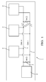
- Figure 1 shows a schematic figure showing a CAN system 1 comprising one or more CAN devices 2 connected by a bus line comprising a pair of twisted lines (4,5) designated CAN Hi (CAN_H), with reference numeral 5, and CAN Lo (CAN_L), designated by reference numeral 4, in the figure.
- a resistance 3 is added to the end of each line to ensure correct and balancing impedances. In a standard, this is 120 ⁇ .
- signal disturbing reflections will be generated at the end of the transmission line if the terminating (load-) impedance is not identical with the corresponding characteristic wave impedance.
- the signal group delay of the whole system should be frequency independent to avoid signal distortion by different transit times for different frequencies.
- the terminating impedances must be real and identical with the characteristic wave impedance of the line. It is preferable in said systems to provide a system with symmetrical, resistive n-port line splitter with correct characteristic wave impedance on all port.
- a line splitter (synonym: power splitter) is realised distributing an incoming signal to a number of outgoing lines, and has to be totally frequency independent concerning the signal bandwidth, it should be realized by resistors only in the first step.
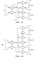
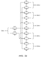
- Figure 2 a to 2 d shows designs of real symmetrical splitters in relation to CAN systems and configurations; balanced to ground for splitter schematics for two, three, four and five output terminals respectively.
- Figure 2a shows an example of a simple star like configuration where a CAN1, CAN2, and CAN 3 communicate (e.g. to send/receive data/signals to and from each other).
- Each of the lines 12a (CAN_H) and 12b (CAN_L) in the line pair from CAN 1 is connected to each of one of the pair of line pairs 11a, 11b in respect of CAN 2 and CAN3.
- the impedance (IN/OUT) seen by all the CAN systems is 120 ⁇ in the example; i.e. the value of impedance (Zin/Zout) seen by CAN1 CAN 2 and CAN3 is 120 ⁇ .
- resistors Ro are added to each line (branch), so between each junction point and CAN.
- the value of the resistors is 20 ⁇ to provide the overall 120 ⁇ seen by the CANs.
- Figure 2b 2c and 2d shows similar examples of a single star configuration for three, four and five CANs.
- the (Hi Lo) the lines from CAN A are split into corresponding lines for each of the other CANs.
- the resistance values of Ro are selected appropriately to provide a seen IN/OUT resistance/impedance of 120 ⁇ .
- the reference numerals refer to like components in figure 2a .
- FIG. 3 shows a typical "double star" topology CAN system for automotive use constructed with such splitter as described above.
- Star 6 is comprised of cans CAN1 CAN 2 CAN3 CAN4 and the other star 7 comprises CAN 5, CAN 6 CAN 7.
- the CANs themselves are not shown for clarity.
- Each of the lines of the lines pair (in respect to the Hi line 12a and Lo line12b) from each CAN in star 6 is connected, via balancing resistor, to a junction point so as they are connected respectively to the respective one of a pair of common lines (10a,10b) of an e.g. twisted pair 8 connects a corresponding (e.g. twisted) pair of lines 9 from star 7.
- balancing resistor (Ro7- Ro14) is provided between each CAN and the junction point. Further between each junction point ( from which one of each line form the CANs is connected to) and the respective Hi and Lo lines 10a and 10b is included balancing resistors.
- Star 5 is connected to star 6 by e.g. a twisted cable as mentioned.
- Star 7 has a similar (mirror image) configuration).
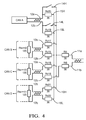
- Figure 4 shows one example of the current invention.
- the figure shows a single star CAN configuration. This can be connected to further CAN devices or a further star like systems to form a double star via twisted pair 11a, 11b. where 11 a is the Hi line and 11b is the Lo line.
- each of these CANs has a line pair (12a 12 b) with respective to Hi and Lo lines, which may be in the form of twisted cable pair. So these pairs comprise a Hi and Lo line (CAN_H and CAN_L). For all the CANs, one of each pair of these lines is connected to a respective common line/junction 16. In the figure the common line/junction line for each of the high side lines is designated 16H and for the low side lines the common line/junction is designated 16L.
- each of the lines CAN_H and CAN_L is connected to the common junction/common line (16H and 16L respectively) via a balancing resistor 15 and a switch 14 (arranged in parallel).
- the resistor and switch in respect of the CAN H lines is designated 15H and 14H respectively and for the low side line CAN L designated 15L and 14L respectively.
- Each one of the common junction/line (points)16H, 16L are connected to the respective one of the twisted pair (11a,11b) respectively via balancing resistors Ri5 and Ri6.
- any or all of CANs of CAN B, CAN C, CAN D may include an arrangement as for CAN A, i.e. the resistors Ro20, Ro19, Ro 18, Ro17, Ro16, Ro15 Ro21 Ro22 may also include bypass switches, so as to provide bypass of the signal from these resistors for each of the high and low lines (CAN_H and CAN_L) from each CAN respectively.
- the switch may be self-operating (automatic)in respect that the switch closes when it detects that a signal is being transmitted from the CAN A.
- this can be used to trigger the switch.
- bypass switches and methodology solve the problem of the aforementioned amplitude problem; by allowing the series resistances of the splitter network to be by-passed in the dominant line condition when that corresponding branch is in transmitting state. This prevents excessive attenuation of the n-port line splitter
- Figure 5a to c shows embodiments of the invention showing how the switching function can be provided.
- FIG. 5a shows a system of threes CAN devices, CAN A, CAN B and CAN C forming a single star configuration.
- the network is shown and the CAN devices themselves are not shown for clarity.
- the figure is similar to figure 4 except a "mirror image".
- each line of the line pair with respect to Hi and Lo lines (12a , 12b) from each CAN is connected to a respective common line/junction, which is connected, via balancing resistors Ri1 and Ri2, to a respective (e.g. twisted) line pair lines in respect of Hi and Lo lines (11a, 11b), over which signals can be transmitted to communicate to or from a CAN device or a similar star system; i.e. over a single twisted pair..
- a balancing resistor for CAN A these have respectively references Ro6 and Ro5
- switch means which in this example is a Schottky diode 18. So the effective switches are provided by Schottky diode in parallel with resistors. Thus, considering the switches 14H and 14L in figure 4 these may comprise Schottky diodes.
- Figure 5b shows a figure similar to figure 5a . It shows the configuration in respect of a number of connected CANs in a single star structure. The figure has corresponding reference numerals to components in figure 4 .
- the switches comprise of a pair of (bi-polar)transistor) and associated resistors configured arranged as shown.
- balancing resistors 15H and 15L between the common line/junctions and the CANs.
- the switch comprises a first (PNP) bipolar transistor Q1, the emitter and collector of which are connected to either side of balancing resistors 15H.
- the base of this transistor is connected to a point on the low side line 12b, via resistor Rb at a point between the CAN A and resistor 15L.
- a second (NPN) transistor Q2 is connected as shown where the collector and emitter are connected to point on either side of resistor 15L, and the base is connected via additional resistor Rb1 to a point hi side line 12a, to a point between the resistor 15H and CAN A.
- the emitter of Q2 is connected to the CAN A side of resistor 15L and collector to the other side of the resistor 15L; the emitter of Q1 is connected to the CAN A side of resistor 15H and collector to the other side of the resistor 15H.
- FIG. 5c shows a figure similar to figure 5b and 5a .
- the figure has corresponding reference numerals to identical components.
- the switches comprise of two MOSFETs M1 and M2 configured as shown.
- balancing resistors 15H and 15L between the respective common line/junctions 16H and 16L, and the CANs.
- the switch comprises a first (P channel) MOSFET, M1, the source and drain of which are connected to either side of balancing resistor 15H.
- the gate of MOSFET M1 is connected to a point on the low side line 12b, at a point between CAN A and resistor 15L.
- a second (N channel) MOSFET M2 is connected as shown where the source and drain are connected to point on either side of resistor 15L, and the gate is connected to a point on the high side line 12a, to a point between the resistor 15H and CAN A.
- the source of M1 is connected to the CAN A side of resistor 15L and drain to the other side of the resistor 15L; the source of M2 is connected to the CAN A side of resistor 15H and drain to the other side of the resistor 15H.
- MOSFETs providing a low "switch on” resistance compared to the forward voltage of the diode and the saturation voltage of the bipolar transistor.
Landscapes
- Engineering & Computer Science (AREA)
- Computer Networks & Wireless Communication (AREA)
- Signal Processing (AREA)
- Power Engineering (AREA)
- Dc Digital Transmission (AREA)
- Small-Scale Networks (AREA)
Abstract
Description
- The invention relates to bus systems for transmitting data to and from a plurality of remote units via a bus line. It has particular application in (CAN) Controller Area Network systems. A CAN bus is a vehicle bus standard, designed to allow microcontrollers and devices to communicate with each other in applications without a host computer,
- For nearly twenty years CAN has been the dominating bus system within the automotive industry. With ever growing demand concerning data throughput fast CAN and CAN FD (flexible data) rate systems, these systems will be implemented more and more in future modem car communication. The physical back bone of the original CAN system is defined by ISO11898: a linear transmission line build by a twisted pair cable with a characteristic wave impedance of 120 Ω and a proper termination at both ends. The connection to the different CAN devices along the line is accomplished by short stub lines which have a negligible influence on the wave impedance of the system.
- However this linear topology is not optimal for the typical car cable harness, and attempts have been made to create a reliable star- or double star topology with one distribution point within the motor compartment and the second one in the passenger cabin for instance. To avoid heavy signal distortion by ringing and reflected signals on the line and to achieve independency from the length of the cable branches, the characteristic wave impedance must be respected or at least approximated in all sections of the CAN lines.
- Patent Application
DE 4235616A1 proposes a solution for this problem at least for lower transmission rates. Approximation of the wave impedance is accomplished by implementing proper ferrite beads with frequency dependent attenuation at the junction points. This solution will function quite fine with low and medium range data rates. With transmission speeds up to 5 Mbit/s the distortions and signal attenuations will become insurmountable. These high data speeds with clock rates of 200 ns need a more sophisticated adaptation of the characteristic wave impedance and enhancement of the signal amplitude. - It is an object of the invention to overcome these problems. It is in a particular object to overcome the problems of signal distortion due to reflections and ringing at high data rates and inacceptable signal attenuation.
- A CAN arrangement comprising at least one CAN, said CAN having a pair of communication lines, each adapted for communication/connection with one or more further CANs, via respective lines of a common connection line pair, and including first and second balancing resistor located between each of said pair of CAN communication lines and said respective common connection lines, and further including switch means located in parallel with said balancing resistor adapted to provide a by-pass path of signals away from said resistor.
- Said switch means may be adapted to provide a bypass path for signals when said CAN is active or in transmitting mode.
- Said switches may comprise Schottky diodes or a pair of transistors located in parallel and each connected to each line of said pair of communication lines. Said transistors may be bipolar transistors or MOSFETs.
- Where said transistors are bipolar transistors, the collector and emitter terminals of the first transistor may be connected to either side of the first balancing resistor located on the first of said pair of communication line and the collector and emitter terminals of second transistor may be connected to either side of the balancing resistor located on the second of said pair of communication lines.
- Wherein said transistors are MOSFETs, the source and drain terminals of the first MOSFET may be connected to either side of a first balancing resistor and the source and drain of said second MOSFET may be connected to either side of a second balancing resistor.
- A CAN arrangement as comprising a plurality of CANs, each of said CANs having a pair of communication lines which are connected to a respective one of a pair of common connection lines/junctions, so as to form a single star arrangement, where at least one CAN comprises a CAN arrangement as above. A CAN system may comprise at least two CAN arrangements as above connected via a single line pair so as to form a multiple star arrangement.
- The Invention will now be described by way of example and with reference to the following figures of which:
-
Figure 1 shows a schematic figure showing a CAN system; -
Figure 2 a to 2 d shows designs of real symmetrical splitters in relation to CAN systems and configurations; -
Figure 3 shows a typical "double star" topology CAN system; -
Figure 4 shows one example of a CAN arrangement according to the current invention; and -
Figure 5a to c shows particular embodiments of the invention. -
Figure 1 shows a schematic figure showing aCAN system 1 comprising one ormore CAN devices 2 connected by a bus line comprising a pair of twisted lines (4,5) designated CAN Hi (CAN_H), withreference numeral 5, and CAN Lo (CAN_L), designated byreference numeral 4, in the figure. Aresistance 3 is added to the end of each line to ensure correct and balancing impedances. In a standard, this is 120Ω. According to transmission line theory signal disturbing reflections will be generated at the end of the transmission line if the terminating (load-) impedance is not identical with the corresponding characteristic wave impedance. As a CAN data stream, especially with high data rate, consists of a broadband frequency spectrum, the signal group delay of the whole system should be frequency independent to avoid signal distortion by different transit times for different frequencies. - As the line properties are given (120 Ω symmetrical twisted pair cable with known capacity, resistance and inductance per meter) the terminating impedances must be real and identical with the characteristic wave impedance of the line. It is preferable in said systems to provide a system with symmetrical, resistive n-port line splitter with correct characteristic wave impedance on all port.
- If it is assumed that a line splitter (synonym: power splitter) is realised distributing an incoming signal to a number of outgoing lines, and has to be totally frequency independent concerning the signal bandwidth, it should be realized by resistors only in the first step.
-
Figure 2 a to 2 d shows designs of real symmetrical splitters in relation to CAN systems and configurations; balanced to ground for splitter schematics for two, three, four and five output terminals respectively. -
Figure 2a shows an example of a simple star like configuration where a CAN1, CAN2, andCAN 3 communicate (e.g. to send/receive data/signals to and from each other). Each of thelines 12a (CAN_H) and 12b (CAN_L) in the line pair fromCAN 1 is connected to each of one of the pair ofline pairs CAN 2 and CAN3. There are therefore two junction points A and B. Thus the signal/line(s) from CAN1 are effectively split. The impedance (IN/OUT) seen by all the CAN systems is 120Ω in the example; i.e. the value of impedance (Zin/Zout) seen by CAN1CAN 2 and CAN3 is 120Ω. In the example, to provide effective impedances as seen by the CANs of 120Ω each, resistors Ro are added to each line (branch), so between each junction point and CAN. In the example the value of the resistors is 20Ω to provide the overall 120Ω seen by the CANs. -
Figure 2b 2c and2d shows similar examples of a single star configuration for three, four and five CANs. Here the (Hi Lo) the lines from CAN A are split into corresponding lines for each of the other CANs. In these cases, the resistance values of Ro are selected appropriately to provide a seen IN/OUT resistance/impedance of 120Ω. The reference numerals refer to like components infigure 2a . -
Figure 3 shows a typical "double star" topology CAN system for automotive use constructed with such splitter as described above. Star 6 is comprised of cans CAN1 CAN 2 CAN3 CAN4 and theother star 7 comprisesCAN 5, CAN 6 CAN 7. The CANs themselves are not shown for clarity. Each of the lines of the lines pair (in respect to theHi line 12a and Lo line12b) from each CAN instar 6 is connected, via balancing resistor, to a junction point so as they are connected respectively to the respective one of a pair of common lines (10a,10b) of an e.g.twisted pair 8 connects a corresponding (e.g. twisted) pair oflines 9 fromstar 7. Between each CAN and the junction point a balancing resistor (Ro7- Ro14) is provided. Further between each junction point ( from which one of each line form the CANs is connected to) and the respective Hi andLo lines star 6 by e.g. a twisted cable as mentioned. Star 7 has a similar (mirror image) configuration). - The different line lengths are not critical provided that the overall damping factor will not become excessive (LTRA meaning "Lossy Transmission Line", i.e. twisted pair cable connection). There may be resistors located in parallel between each Hi and Lo lines at the CAN terminals Shown here as Rterm1 - Rterm7)
- Simulating this topology by LT Spice or System Vision with CAN signals delivers excellent signal integrity without any ringing or reflections on all ports even with different line lengths as was expected because of meticulously respecting the characteristic wave impedance in any single point of the network structure. But a clear disadvantage is the heavy and unacceptable signal attenuation especially between the "far-out ports" of the network. A solution to this effective problem of excessive damping was to raise the signal level of the transmitting branch by adequate means; however this can cause considerable distortion.
-
Figure 4 shows one example of the current invention. The figure shows a single star CAN configuration. This can be connected to further CAN devices or a further star like systems to form a double star viatwisted pair - On the left hand side of the figure are shown connections to four CAN device, CAN A, CAN B, CAN C and CAN D. Only CAN A is shown for the purposes of illustrating the invention. As is similar to
figure 3 , each of these CANs has a line pair (12a 12 b) with respective to Hi and Lo lines, which may be in the form of twisted cable pair. So these pairs comprise a Hi and Lo line (CAN_H and CAN_L). For all the CANs, one of each pair of these lines is connected to a respective common line/junction 16. In the figure the common line/junction line for each of the high side lines is designated 16H and for the low side lines the common line/junction is designated 16L. As can be seen for CAN A, each of the lines CAN_H and CAN_L is connected to the common junction/common line (16H and 16L respectively) via a balancing resistor 15 and a switch 14 (arranged in parallel). In the figure the resistor and switch in respect of the CAN H lines is designated 15H and 14H respectively and for the low side line CAN L designated 15L and 14L respectively. - Each one of the common junction/line (points)16H, 16L are connected to the respective one of the twisted pair (11a,11b) respectively via balancing resistors Ri5 and Ri6.
- So all the CANs are connected to common lines/junctions via balancing resistors Ro15 to Ro22. It is to be noted that Ro20 also the designation as 15H and Ro19 the
designation 15L. - It is to be noted that although not shown any or all of CANs of CAN B, CAN C, CAN D, may include an arrangement as for CAN A, i.e. the resistors Ro20, Ro19,
Ro 18, Ro17, Ro16, Ro15 Ro21 Ro22 may also include bypass switches, so as to provide bypass of the signal from these resistors for each of the high and low lines (CAN_H and CAN_L) from each CAN respectively. - In operation, when CAN A is transmitting, the switch14 H and 14L are closed to provide a bypass signal path i.e. by-passing the
resistors - It is to be noted that in examples the switch may be self-operating (automatic)in respect that the switch closes when it detects that a signal is being transmitted from the CAN A. In these examples there is an exploitable voltage shift between CAN_Land CAN_H when changing from recessive to dominant state, this can be used to trigger the switch.
- The bypass switches and methodology solve the problem of the aforementioned amplitude problem; by allowing the series resistances of the splitter network to be by-passed in the dominant line condition when that corresponding branch is in transmitting state. This prevents excessive attenuation of the n-port line splitter
-
Figure 5a to c shows embodiments of the invention showing how the switching function can be provided. -
Figure 5a shows a system of threes CAN devices, CAN A, CAN B and CAN C forming a single star configuration. The network is shown and the CAN devices themselves are not shown for clarity. The figure is similar tofigure 4 except a "mirror image". As before each line of the line pair with respect to Hi and Lo lines (12a , 12b) from each CAN is connected to a respective common line/junction, which is connected, via balancing resistors Ri1 and Ri2, to a respective (e.g. twisted) line pair lines in respect of Hi and Lo lines (11a, 11b), over which signals can be transmitted to communicate to or from a CAN device or a similar star system; i.e. over a single twisted pair.. - As is similar to
figure 4 between each of the common line/junction (16H and 16L) and each of respective CAN H and CAN L lines (12a and 12b), is located a balancing resistor (for CAN A these have respectively references Ro6 and Ro5) and switch means, which in this example is aSchottky diode 18. So the effective switches are provided by Schottky diode in parallel with resistors. Thus, considering theswitches figure 4 these may comprise Schottky diodes. -
Figure 5b shows a figure similar tofigure 5a . It shows the configuration in respect of a number of connected CANs in a single star structure. The figure has corresponding reference numerals to components infigure 4 . - The switches comprise of a pair of (bi-polar)transistor) and associated resistors configured arranged as shown. For each CAN with respect to Hi and Lo lines there are provided balancing
resistors low side line 12b, via resistor Rb at a point between the CAN A andresistor 15L. A second (NPN) transistor Q2 is connected as shown where the collector and emitter are connected to point on either side ofresistor 15L, and the base is connected via additional resistor Rb1 to a pointhi side line 12a, to a point between theresistor 15H and CAN A. For the purpose of completeness the emitter of Q2 is connected to the CAN A side ofresistor 15L and collector to the other side of theresistor 15L; the emitter of Q1 is connected to the CAN A side ofresistor 15H and collector to the other side of theresistor 15H. - Transmission from the CAN A effectively activates the transistor (switches) such that signals can pass through them between CAN A and other CANs in the system, bypassing
resistors -
Figure 5c shows a figure similar tofigure 5b and5a . The figure has corresponding reference numerals to identical components. The switches comprise of two MOSFETs M1 and M2 configured as shown. For each CAN with respect to Hi and Lo lines (12a and 12b respectively) there are provided balancingresistors junctions resistor 15H. The gate of MOSFET M1 is connected to a point on thelow side line 12b, at a point between CAN A andresistor 15L. A second (N channel) MOSFET M2, is connected as shown where the source and drain are connected to point on either side ofresistor 15L, and the gate is connected to a point on thehigh side line 12a, to a point between theresistor 15H and CAN A. For the purpose of completeness the source of M1 is connected to the CAN A side ofresistor 15L and drain to the other side of theresistor 15L; the source of M2 is connected to the CAN A side ofresistor 15H and drain to the other side of theresistor 15H. - Good results with very high attenuation values of the resistive networks are achieved by MOSFETs providing a low "switch on" resistance compared to the forward voltage of the diode and the saturation voltage of the bipolar transistor.
- Maximum robustness and cost effectivity can be achieved of course with the implementation of suitable Schottky diodes.
- Extensive simulations with LT-Spice were performed on a typical automotive "double star" configuration with realistic cable lengths. Excellent results were obtained with respect to pulse forming and amplitude values on all receiving ports. Bus arbitration was simulated with three CAN transceivers competing for bus access at the same time. There was no signal conflict at the active elements due to the inherent dominant/recessive line philosophy. The peak power losses at the switching elements during bus arbitration procedure have been under research and were found to be far below their limits. Examples of the invention provide an implementation of a symmetrical, resistive n-port line splitter with correct characteristic wave impedance on all ports and countermeasures against excessive attenuation of the n-port line splitter to allow implementation of star-like or double star-like topologies
Claims (9)
- A CAN arrangement comprising at least one CAN, said CAN having a pair of communication lines, each adapted for communication/connection with one or more further CANs, via respective lines of a common connection line pair, and including first and second balancing resistor located between each of said pair of CAN communication lines and said respective common connection lines, and further including switch means located in parallel with said balancing resistor adapted to provide a by-pass path of signals away from said resistor.
- An arrangement as claimed in claim 1 wherein said switch means is adapted to provide a bypass path for signals when said CAN is active or in transmitting mode.
- A CAN arrangement as claimed in claims 1 or 2 wherein said switches comprise Schottky diodes.
- A CAN arrangement as claimed in claims 1 or 2 wherein said switches comprises a pair of transistors located in parallel and each connected to each line of said pair of communication lines.
- A CAN arrangement as claimed in claim 4 wherein said transistors are bipolar transistors or MOSFETs.
- A CAN arrangement as claimed in claim 4 or 5 wherein said transistors are bipolar transistors and where the collector and emitter terminals of the first transistor are connected to either side of the first balancing resistor located on the first of said pair of communication line and the collector and emitter terminals of second transistor are connected to either side of the balancing resistor located on the second of said pair of communication lines.
- A CAN arrangement as claimed in claim 4 or 5 wherein said transistors are MOSFETs and where the source and drain terminals of the first MOSFET are connected to either side of a first balancing resistor and the source and drain of said second MOSFET are connected to either side of a second balancing resistor.
- A CAN arrangement as comprising a plurality of CANs, each of said CANs having a pair of communication lines which are connected to a respective one of a pair of common connection lines/junctions, so as to form a single star arrangement, where at least one CAN comprises a CAN arrangement as claimed in claim 1 to 7.
- A CAN system comprising at least two CAN arrangements as claimed in claim 8 connected via a single line pair so as to form a multiple star arrangement.
Priority Applications (1)
| Application Number | Priority Date | Filing Date | Title |
|---|---|---|---|
| EP16190671.4A EP3300310B1 (en) | 2016-09-26 | 2016-09-26 | Controller area network (can) system |
Applications Claiming Priority (1)
| Application Number | Priority Date | Filing Date | Title |
|---|---|---|---|
| EP16190671.4A EP3300310B1 (en) | 2016-09-26 | 2016-09-26 | Controller area network (can) system |
Publications (2)
| Publication Number | Publication Date |
|---|---|
| EP3300310A1 true EP3300310A1 (en) | 2018-03-28 |
| EP3300310B1 EP3300310B1 (en) | 2019-06-19 |
Family
ID=57046997
Family Applications (1)
| Application Number | Title | Priority Date | Filing Date |
|---|---|---|---|
| EP16190671.4A Active EP3300310B1 (en) | 2016-09-26 | 2016-09-26 | Controller area network (can) system |
Country Status (1)
| Country | Link |
|---|---|
| EP (1) | EP3300310B1 (en) |
Cited By (3)
| Publication number | Priority date | Publication date | Assignee | Title |
|---|---|---|---|---|
| WO2019199990A1 (en) * | 2018-04-11 | 2019-10-17 | Phillips Connect Technologies Llc | Modular harness system |
| US10647369B2 (en) | 2016-10-07 | 2020-05-12 | Phillips Connect Technologies Llc | Modular harness system |
| US11912359B2 (en) | 2016-10-07 | 2024-02-27 | Phillips Connect Technologies Llc | Smart trailer system |
Citations (3)
| Publication number | Priority date | Publication date | Assignee | Title |
|---|---|---|---|---|
| DE1295662B (en) * | 1966-09-12 | 1969-05-22 | Euratom | Electrical branch circuit in high frequency cable networks |
| WO1988000779A1 (en) * | 1986-07-23 | 1988-01-28 | Ncr Corporation | Data communications system having noise reduction means |
| DE4235616A1 (en) | 1991-10-26 | 1993-04-29 | Daimler Benz Ag | DATA COMMUNICATION SYSTEM |
-
2016
- 2016-09-26 EP EP16190671.4A patent/EP3300310B1/en active Active
Patent Citations (3)
| Publication number | Priority date | Publication date | Assignee | Title |
|---|---|---|---|---|
| DE1295662B (en) * | 1966-09-12 | 1969-05-22 | Euratom | Electrical branch circuit in high frequency cable networks |
| WO1988000779A1 (en) * | 1986-07-23 | 1988-01-28 | Ncr Corporation | Data communications system having noise reduction means |
| DE4235616A1 (en) | 1991-10-26 | 1993-04-29 | Daimler Benz Ag | DATA COMMUNICATION SYSTEM |
Cited By (4)
| Publication number | Priority date | Publication date | Assignee | Title |
|---|---|---|---|---|
| US10647369B2 (en) | 2016-10-07 | 2020-05-12 | Phillips Connect Technologies Llc | Modular harness system |
| US11912359B2 (en) | 2016-10-07 | 2024-02-27 | Phillips Connect Technologies Llc | Smart trailer system |
| US12459587B2 (en) | 2016-10-07 | 2025-11-04 | Phillips Connect Technologies Llc | Smart trailer system |
| WO2019199990A1 (en) * | 2018-04-11 | 2019-10-17 | Phillips Connect Technologies Llc | Modular harness system |
Also Published As
| Publication number | Publication date |
|---|---|
| EP3300310B1 (en) | 2019-06-19 |
Similar Documents
| Publication | Publication Date | Title |
|---|---|---|
| US5734658A (en) | Data communication system | |
| US7884648B2 (en) | Pseudo-differential interfacing device having a switching circuit | |
| CN105684370B (en) | Subscriber station of a bus system and method for reducing wired emissions in a bus system | |
| EP3300310B1 (en) | Controller area network (can) system | |
| US4943739A (en) | Non-reflecting transmission line termination | |
| CN104133800A (en) | Device and method for an enhanced driver mode for a shared bus | |
| US20170048085A1 (en) | Ethernet and OFDM Multiplexing on UTP Cable | |
| US6414953B1 (en) | Multi-protocol cross connect switch | |
| EP1920503A2 (en) | Bridging coaxial cable networks | |
| US8222925B2 (en) | Multimode Ethernet line driver | |
| US20060133598A1 (en) | Isolation of transmit and receive signals in full-duplex communication systems | |
| US7592880B2 (en) | Communicating over coaxial cable networks | |
| US4775864A (en) | Local area network with multiple node bus topology | |
| JP2845480B2 (en) | Signal distribution method | |
| US10454722B2 (en) | In-vehicle processing device and in-vehicle system | |
| US20020130680A1 (en) | Method and apparatus for terminating emitter coupled logic (ECL) transceivers | |
| EP4498611A1 (en) | Impedance conversion device for vehicle-mounted gigabit ethernet chip adaptive coaxial cable transmission | |
| US4841295A (en) | Local area network with biasing arrangement for facilitating access contention between work stations connected to a common bus | |
| WO2009007864A1 (en) | Pseudo-differential interfacing device having a balancing circuit | |
| US20210409003A1 (en) | Reflection attenuation device for a bus of a bus system, and method for attenuating reflections during a data transfer in a bus system | |
| KR20130113034A (en) | Can bus system | |
| US9024701B1 (en) | Method and apparatus for controlling a line side impedance in a network device | |
| US12603947B2 (en) | Network port circuit | |
| CN115292228B (en) | A bus communication method and system based on avionics fault injection | |
| US6404299B1 (en) | Devices, methods, and systems for network hub partial termination |
Legal Events
| Date | Code | Title | Description |
|---|---|---|---|
| PUAI | Public reference made under article 153(3) epc to a published international application that has entered the european phase |
Free format text: ORIGINAL CODE: 0009012 |
|
| STAA | Information on the status of an ep patent application or granted ep patent |
Free format text: STATUS: THE APPLICATION HAS BEEN PUBLISHED |
|
| AK | Designated contracting states |
Kind code of ref document: A1 Designated state(s): AL AT BE BG CH CY CZ DE DK EE ES FI FR GB GR HR HU IE IS IT LI LT LU LV MC MK MT NL NO PL PT RO RS SE SI SK SM TR |
|
| AX | Request for extension of the european patent |
Extension state: BA ME |
|
| STAA | Information on the status of an ep patent application or granted ep patent |
Free format text: STATUS: REQUEST FOR EXAMINATION WAS MADE |
|
| 17P | Request for examination filed |
Effective date: 20180928 |
|
| RBV | Designated contracting states (corrected) |
Designated state(s): AL AT BE BG CH CY CZ DE DK EE ES FI FR GB GR HR HU IE IS IT LI LT LU LV MC MK MT NL NO PL PT RO RS SE SI SK SM TR |
|
| RAP1 | Party data changed (applicant data changed or rights of an application transferred) |
Owner name: APTIV TECHNOLOGIES LIMITED |
|
| GRAP | Despatch of communication of intention to grant a patent |
Free format text: ORIGINAL CODE: EPIDOSNIGR1 |
|
| STAA | Information on the status of an ep patent application or granted ep patent |
Free format text: STATUS: GRANT OF PATENT IS INTENDED |
|
| RIC1 | Information provided on ipc code assigned before grant |
Ipc: H04L 12/44 20060101AFI20181214BHEP Ipc: H04B 3/00 20060101ALI20181214BHEP Ipc: H04L 12/40 20060101ALN20181214BHEP |
|
| RIC1 | Information provided on ipc code assigned before grant |
Ipc: H04B 3/00 20060101ALI20190108BHEP Ipc: H04L 12/44 20060101AFI20190108BHEP Ipc: H04L 12/40 20060101ALN20190108BHEP |
|
| INTG | Intention to grant announced |
Effective date: 20190123 |
|
| GRAS | Grant fee paid |
Free format text: ORIGINAL CODE: EPIDOSNIGR3 |
|
| GRAA | (expected) grant |
Free format text: ORIGINAL CODE: 0009210 |
|
| STAA | Information on the status of an ep patent application or granted ep patent |
Free format text: STATUS: THE PATENT HAS BEEN GRANTED |
|
| AK | Designated contracting states |
Kind code of ref document: B1 Designated state(s): AL AT BE BG CH CY CZ DE DK EE ES FI FR GB GR HR HU IE IS IT LI LT LU LV MC MK MT NL NO PL PT RO RS SE SI SK SM TR |
|
| REG | Reference to a national code |
Ref country code: GB Ref legal event code: FG4D |
|
| REG | Reference to a national code |
Ref country code: CH Ref legal event code: EP |
|
| REG | Reference to a national code |
Ref country code: IE Ref legal event code: FG4D |
|
| REG | Reference to a national code |
Ref country code: DE Ref legal event code: R096 Ref document number: 602016015452 Country of ref document: DE |
|
| REG | Reference to a national code |
Ref country code: AT Ref legal event code: REF Ref document number: 1146915 Country of ref document: AT Kind code of ref document: T Effective date: 20190715 |
|
| REG | Reference to a national code |
Ref country code: NL Ref legal event code: MP Effective date: 20190619 |
|
| PG25 | Lapsed in a contracting state [announced via postgrant information from national office to epo] |
Ref country code: HR Free format text: LAPSE BECAUSE OF FAILURE TO SUBMIT A TRANSLATION OF THE DESCRIPTION OR TO PAY THE FEE WITHIN THE PRESCRIBED TIME-LIMIT Effective date: 20190619 Ref country code: SE Free format text: LAPSE BECAUSE OF FAILURE TO SUBMIT A TRANSLATION OF THE DESCRIPTION OR TO PAY THE FEE WITHIN THE PRESCRIBED TIME-LIMIT Effective date: 20190619 Ref country code: LT Free format text: LAPSE BECAUSE OF FAILURE TO SUBMIT A TRANSLATION OF THE DESCRIPTION OR TO PAY THE FEE WITHIN THE PRESCRIBED TIME-LIMIT Effective date: 20190619 Ref country code: FI Free format text: LAPSE BECAUSE OF FAILURE TO SUBMIT A TRANSLATION OF THE DESCRIPTION OR TO PAY THE FEE WITHIN THE PRESCRIBED TIME-LIMIT Effective date: 20190619 Ref country code: NO Free format text: LAPSE BECAUSE OF FAILURE TO SUBMIT A TRANSLATION OF THE DESCRIPTION OR TO PAY THE FEE WITHIN THE PRESCRIBED TIME-LIMIT Effective date: 20190919 Ref country code: AL Free format text: LAPSE BECAUSE OF FAILURE TO SUBMIT A TRANSLATION OF THE DESCRIPTION OR TO PAY THE FEE WITHIN THE PRESCRIBED TIME-LIMIT Effective date: 20190619 |
|
| REG | Reference to a national code |
Ref country code: LT Ref legal event code: MG4D |
|
| PG25 | Lapsed in a contracting state [announced via postgrant information from national office to epo] |
Ref country code: BG Free format text: LAPSE BECAUSE OF FAILURE TO SUBMIT A TRANSLATION OF THE DESCRIPTION OR TO PAY THE FEE WITHIN THE PRESCRIBED TIME-LIMIT Effective date: 20190919 Ref country code: LV Free format text: LAPSE BECAUSE OF FAILURE TO SUBMIT A TRANSLATION OF THE DESCRIPTION OR TO PAY THE FEE WITHIN THE PRESCRIBED TIME-LIMIT Effective date: 20190619 Ref country code: RS Free format text: LAPSE BECAUSE OF FAILURE TO SUBMIT A TRANSLATION OF THE DESCRIPTION OR TO PAY THE FEE WITHIN THE PRESCRIBED TIME-LIMIT Effective date: 20190619 Ref country code: GR Free format text: LAPSE BECAUSE OF FAILURE TO SUBMIT A TRANSLATION OF THE DESCRIPTION OR TO PAY THE FEE WITHIN THE PRESCRIBED TIME-LIMIT Effective date: 20190920 |
|
| REG | Reference to a national code |
Ref country code: AT Ref legal event code: MK05 Ref document number: 1146915 Country of ref document: AT Kind code of ref document: T Effective date: 20190619 |
|
| PG25 | Lapsed in a contracting state [announced via postgrant information from national office to epo] |
Ref country code: EE Free format text: LAPSE BECAUSE OF FAILURE TO SUBMIT A TRANSLATION OF THE DESCRIPTION OR TO PAY THE FEE WITHIN THE PRESCRIBED TIME-LIMIT Effective date: 20190619 Ref country code: PT Free format text: LAPSE BECAUSE OF FAILURE TO SUBMIT A TRANSLATION OF THE DESCRIPTION OR TO PAY THE FEE WITHIN THE PRESCRIBED TIME-LIMIT Effective date: 20191021 Ref country code: NL Free format text: LAPSE BECAUSE OF FAILURE TO SUBMIT A TRANSLATION OF THE DESCRIPTION OR TO PAY THE FEE WITHIN THE PRESCRIBED TIME-LIMIT Effective date: 20190619 Ref country code: SK Free format text: LAPSE BECAUSE OF FAILURE TO SUBMIT A TRANSLATION OF THE DESCRIPTION OR TO PAY THE FEE WITHIN THE PRESCRIBED TIME-LIMIT Effective date: 20190619 Ref country code: CZ Free format text: LAPSE BECAUSE OF FAILURE TO SUBMIT A TRANSLATION OF THE DESCRIPTION OR TO PAY THE FEE WITHIN THE PRESCRIBED TIME-LIMIT Effective date: 20190619 Ref country code: RO Free format text: LAPSE BECAUSE OF FAILURE TO SUBMIT A TRANSLATION OF THE DESCRIPTION OR TO PAY THE FEE WITHIN THE PRESCRIBED TIME-LIMIT Effective date: 20190619 Ref country code: AT Free format text: LAPSE BECAUSE OF FAILURE TO SUBMIT A TRANSLATION OF THE DESCRIPTION OR TO PAY THE FEE WITHIN THE PRESCRIBED TIME-LIMIT Effective date: 20190619 |
|
| PG25 | Lapsed in a contracting state [announced via postgrant information from national office to epo] |
Ref country code: SM Free format text: LAPSE BECAUSE OF FAILURE TO SUBMIT A TRANSLATION OF THE DESCRIPTION OR TO PAY THE FEE WITHIN THE PRESCRIBED TIME-LIMIT Effective date: 20190619 Ref country code: IS Free format text: LAPSE BECAUSE OF FAILURE TO SUBMIT A TRANSLATION OF THE DESCRIPTION OR TO PAY THE FEE WITHIN THE PRESCRIBED TIME-LIMIT Effective date: 20191019 Ref country code: ES Free format text: LAPSE BECAUSE OF FAILURE TO SUBMIT A TRANSLATION OF THE DESCRIPTION OR TO PAY THE FEE WITHIN THE PRESCRIBED TIME-LIMIT Effective date: 20190619 Ref country code: IT Free format text: LAPSE BECAUSE OF FAILURE TO SUBMIT A TRANSLATION OF THE DESCRIPTION OR TO PAY THE FEE WITHIN THE PRESCRIBED TIME-LIMIT Effective date: 20190619 |
|
| PG25 | Lapsed in a contracting state [announced via postgrant information from national office to epo] |
Ref country code: TR Free format text: LAPSE BECAUSE OF FAILURE TO SUBMIT A TRANSLATION OF THE DESCRIPTION OR TO PAY THE FEE WITHIN THE PRESCRIBED TIME-LIMIT Effective date: 20190619 |
|
| PG25 | Lapsed in a contracting state [announced via postgrant information from national office to epo] |
Ref country code: DK Free format text: LAPSE BECAUSE OF FAILURE TO SUBMIT A TRANSLATION OF THE DESCRIPTION OR TO PAY THE FEE WITHIN THE PRESCRIBED TIME-LIMIT Effective date: 20190619 Ref country code: PL Free format text: LAPSE BECAUSE OF FAILURE TO SUBMIT A TRANSLATION OF THE DESCRIPTION OR TO PAY THE FEE WITHIN THE PRESCRIBED TIME-LIMIT Effective date: 20190619 |
|
| PG25 | Lapsed in a contracting state [announced via postgrant information from national office to epo] |
Ref country code: IS Free format text: LAPSE BECAUSE OF FAILURE TO SUBMIT A TRANSLATION OF THE DESCRIPTION OR TO PAY THE FEE WITHIN THE PRESCRIBED TIME-LIMIT Effective date: 20200224 Ref country code: MC Free format text: LAPSE BECAUSE OF FAILURE TO SUBMIT A TRANSLATION OF THE DESCRIPTION OR TO PAY THE FEE WITHIN THE PRESCRIBED TIME-LIMIT Effective date: 20190619 |
|
| REG | Reference to a national code |
Ref country code: CH Ref legal event code: PL |
|
| REG | Reference to a national code |
Ref country code: DE Ref legal event code: R097 Ref document number: 602016015452 Country of ref document: DE |
|
| PLBE | No opposition filed within time limit |
Free format text: ORIGINAL CODE: 0009261 |
|
| STAA | Information on the status of an ep patent application or granted ep patent |
Free format text: STATUS: NO OPPOSITION FILED WITHIN TIME LIMIT |
|
| PG2D | Information on lapse in contracting state deleted |
Ref country code: IS |
|
| PG25 | Lapsed in a contracting state [announced via postgrant information from national office to epo] |
Ref country code: IE Free format text: LAPSE BECAUSE OF NON-PAYMENT OF DUE FEES Effective date: 20190926 Ref country code: LU Free format text: LAPSE BECAUSE OF NON-PAYMENT OF DUE FEES Effective date: 20190926 Ref country code: LI Free format text: LAPSE BECAUSE OF NON-PAYMENT OF DUE FEES Effective date: 20190930 Ref country code: CH Free format text: LAPSE BECAUSE OF NON-PAYMENT OF DUE FEES Effective date: 20190930 |
|
| 26N | No opposition filed |
Effective date: 20200603 |
|
| REG | Reference to a national code |
Ref country code: BE Ref legal event code: MM Effective date: 20190930 |
|
| PG25 | Lapsed in a contracting state [announced via postgrant information from national office to epo] |
Ref country code: SI Free format text: LAPSE BECAUSE OF FAILURE TO SUBMIT A TRANSLATION OF THE DESCRIPTION OR TO PAY THE FEE WITHIN THE PRESCRIBED TIME-LIMIT Effective date: 20190619 Ref country code: BE Free format text: LAPSE BECAUSE OF NON-PAYMENT OF DUE FEES Effective date: 20190930 |
|
| PG25 | Lapsed in a contracting state [announced via postgrant information from national office to epo] |
Ref country code: CY Free format text: LAPSE BECAUSE OF FAILURE TO SUBMIT A TRANSLATION OF THE DESCRIPTION OR TO PAY THE FEE WITHIN THE PRESCRIBED TIME-LIMIT Effective date: 20190619 |
|
| PG25 | Lapsed in a contracting state [announced via postgrant information from national office to epo] |
Ref country code: HU Free format text: LAPSE BECAUSE OF FAILURE TO SUBMIT A TRANSLATION OF THE DESCRIPTION OR TO PAY THE FEE WITHIN THE PRESCRIBED TIME-LIMIT; INVALID AB INITIO Effective date: 20160926 Ref country code: MT Free format text: LAPSE BECAUSE OF FAILURE TO SUBMIT A TRANSLATION OF THE DESCRIPTION OR TO PAY THE FEE WITHIN THE PRESCRIBED TIME-LIMIT Effective date: 20190619 |
|
| PG25 | Lapsed in a contracting state [announced via postgrant information from national office to epo] |
Ref country code: MK Free format text: LAPSE BECAUSE OF FAILURE TO SUBMIT A TRANSLATION OF THE DESCRIPTION OR TO PAY THE FEE WITHIN THE PRESCRIBED TIME-LIMIT Effective date: 20190619 |
|
| P01 | Opt-out of the competence of the unified patent court (upc) registered |
Effective date: 20230424 |
|
| REG | Reference to a national code |
Ref country code: DE Ref legal event code: R081 Ref document number: 602016015452 Country of ref document: DE Owner name: APTIV TECHNOLOGIES AG, CH Free format text: FORMER OWNER: APTIV TECHNOLOGIES LIMITED, ST. MICHAEL, BB |
|
| PGFP | Annual fee paid to national office [announced via postgrant information from national office to epo] |
Ref country code: DE Payment date: 20250814 Year of fee payment: 10 |
|
| PGFP | Annual fee paid to national office [announced via postgrant information from national office to epo] |
Ref country code: GB Payment date: 20250924 Year of fee payment: 10 |
|
| PGFP | Annual fee paid to national office [announced via postgrant information from national office to epo] |
Ref country code: FR Payment date: 20250908 Year of fee payment: 10 |